
 Open Access Article
 This Open Access Article is licensed under a
 Creative Commons Attribution 3.0 Unported Licence
Ultra-stretchable and shape-memorable ability of an output-boosted triboelectric nanogenerator utilizing highly ordered microdome-crowning thermoplastic polyurethane for a finger-motion detection sensor†
Ngoc Mai
Chau
 ac,
Phuong Mai
Tran
bc,
Thu Ha
Le
ac,
Thi Thai Ha
La
*ac and
Van-Tien
Bui
*ac
ac,
Phuong Mai
Tran
bc,
Thu Ha
Le
ac,
Thi Thai Ha
La
*ac and
Van-Tien
Bui
*ac
aDepartment of Polymer Materials, Polymer Research Center, Faculty of Materials Technology, Ho Chi Minh City University of Technology (HCMUT), 268 Ly Thuong Kiet Street, District 10, Ho Chi Minh City 700000, Vietnam. E-mail: tienbv@hcmut.edu.vn; lathaihapolyme@hcmut.edu.vn
bFaculty of Environment and Natural Resources, Ho Chi Minh City University of Technology (HCMUT), 268 Ly Thuong Kiet Street, District 10, Ho Chi Minh City 700000, Vietnam
cVietnam National University Ho Chi Minh City, Linh Trung Ward, Thu Duc District, Ho Chi Minh City 700000, Vietnam
First published on 4th November 2023
Abstract
We have strategically imprinted hexagonally arranged microdome arrays onto the surface of thermoplastic polyurethane (TPU) to enhance both the output performance and reliability of a triboelectric nanogenerator (TENG). In this study, we present a novel approach, referred to as improved phase separation micromolding (IPS-m-molding), which utilizes a polymer solution replica of honeycomb-concave films created through an improved phase separation process. Beyond offering customizable micropattern arrays, this pioneering technique offers simplicity, scalability, substantial time, and effort savings, thereby effectively surpassing the limitations associated with the existing methods. The microconvex-patterned TPU films obtained by using the present method possess superior elastomeric characteristics, endowing the triboelectret with superior stretchability and remarkable resistance to impacts and compression, particularly notable shape-memory capabilities that facilitate post-frictional deformation recovery. Furthermore, the integration of micropattern arrays onto the TPU surface significantly enhances the TENG's performance, leading to an eight-fold enhancement in the output power compared to a normal flat TENG. More remarkably, this presented TENG based on microconvex TPU demonstrates exceptional durability, enduring a strenuous 50![[thin space (1/6-em)]](https://www.rsc.org/images/entities/char_2009.gif) 000-cycle endurance test while continually increasing the output voltage. This improvement is attributed to the expanded effective contact surface area and enhanced lateral deformability of the micropatterns. This inherently high-performance electret holds immense potential for integration into transparent, stretchable TENGs designed for wearable motion-detecting sensors.
000-cycle endurance test while continually increasing the output voltage. This improvement is attributed to the expanded effective contact surface area and enhanced lateral deformability of the micropatterns. This inherently high-performance electret holds immense potential for integration into transparent, stretchable TENGs designed for wearable motion-detecting sensors.
Introduction
The advancement of 5G technology and the Internet of Things (IoTs) has propelled our society forward. This has entailed an increasing demand for energy resources due to the continuous power consumption of these devices and sensors. Unfortunately, the reliance on traditional fossil fuels is not only environmentally detrimental but also unsustainable due to their finite availability. Consequently, this has catalyzed global researchers to shift their focus towards more sustainable and alternative energy solutions. Among these pioneering energy technologies, triboelectric nanogenerators (TENGs), also recognized as Wang generators, have emerged as a beacon of sustainable energy innovation since their inception in 2012.1 Functioning on the principles of contact electrification and electrostatic induction, TENGs present a groundbreaking and eco-friendly approach to electricity generation. Endowed naturally with a unique set of merits, including a wide range of material selections, high output, cost-effectiveness, light weight, and versatility in operational modes,2–7 TENGs have demonstrated great potential in wasted mechanical energy harvesting from the surrounding environment.In the domain of TENG research, the development of stretchable TENGs has garnered significant attention, thanks to their phenomenal mechanical properties, flexibility, and adaptability to a variety of practical applications. One of the promising material candidates for developing these stretchable TENGs is thermoplastic polyurethane (TPU), owing to its desirable properties such as high transparency, high durability, and excellent resistance to abrasion, chemicals, wear, and weather.8–11 The unique characteristics of TPU make it well-suited for the development of TENGs that can conform to various surfaces and endure mechanical deformations without compromising their functionality. Despite their high mechanical strength, the output performance of TPU-based TENGs remains a challenge due to the low electron-donating ability of TPU in the tribo-series. Hence, several studies have been conducted choosing TPU as the dielectric with modification approaches to boosting outputs of stretchable TENGs including multilayered TPU/silver nanowires/reduced graphene oxide,12 TPU adding carbon black,13 electrospun TPU,14 polydimethylsiloxane diol functionalized TPU,15etc. However, these strategies often involve complex procedures and significant investments, which emphasizes the need to explore alternative methods for modifying the surface features of TPU.
From another perspective, human well-being is the most concerning factor in modern society, leading to a heightened awareness of health protection with smart devices, including wearable sensors regarding health monitoring. In this field, high sensitivity, stretchability, stability, and human compatibility are strictly required,16 attracting much attention from global scientists to innovate the prototypes in terms of both material and model designs for practical utilization of high-performance wearable sensors in the near future. Many studies proposed the use of extravagant materials to enhance the sensitivity of TENG-based sensors for knee motions such as knitting graphene textiles,17 FEP/silicone@carbon black,18 PDMS/galinstan liquid metal nanoparticles,19 and for finger motions such as gold/polyimide/pyramid PDMS,20 PTFE/magnetic poles,21 glove-based TENGs,22 multifunctional coaxial energy fibers with carbon fiber, PVA, PDMS,23 Mxene (T3C2Tx), polydimethylsiloxane, copper/nickel textiles.24 However, these reported sensors are still not sensitive to the desired extent, along with complicated and highly advanced fabricated materials. This strongly inspires the utilization of c-TPU in commercial sensing devices as a versatile but highly sensitive electret.
In this work, an ultra-stretchable surface-patterned thermoplastic polyurethane thin film is rationally designed, to advance the output of triboelectric nanogenerator devices through a newly developed technique, called improved phase separation micromolding. Our novel method highlights its versatility with time-, cost- and effort-savings, effectively overcoming the constraints that have plagued preceding methods but still maintaining the inherent features of TPU such as high flexibility, high impact resistance, biocompatibility, shape-memorable ability, and high elongation. The resulting stretchable microdome-patterned TPU-based TENG is not only a response to the escalating demand for versatile and adaptable energy harvesting solutions, but also a potential to be fabricated in human motion detecting sensors. This opens a new chapter in energy technology, holding immense potential for future breakthroughs in fields such as electronic skin (e-skin), Internet of Things (IoT) sensors, and beyond. In essence, this work represents a significant stride in the realm of sustainable and flexible energy solutions, paving the way for a greener, smarter future.
Experimental
Materials
Thermoplastic polyurethane 65A (TPU; pellets) was kindly supplied from BangTai Co. (Vietnam). Soluble polyimide (PI; powder) was purchased from Alfa Aesar (USA). Chloroform (anhydrous, stabilized with amylenes; 99.8%), methanol (anhydrous; 99.8%), and tetrahydrofuran (THF; 99%) were all purchased from Sigma Aldrich (USA). Copper foils were obtained from Nhat Phat Co. (Vietnam) and cleaned in turn with a 0.1 M sulfuric acid solution and distilled water before being blow-dried in N2 gas prior to use. Polydimethylsiloxane (PDMS, SYLGARD™ 184 Silicone Elastomer) and its curing agent were obtained from Dow and thoroughly mixed prior to use.Fabrication of microdome-patterned TPU
Initially, 3.13 g of TPU were dissolved in 20 mL of THF and stirred magnetically at 600 rpm for 4 hours to produce a homogeneous 15 wt% TPU solution. This transparent solution was then allowed to stabilize at room temperature for 2 hours. In parallel, a honeycomb poly(vinyl alcohol) film (hc-PVA) was crafted using the improved phase separation process and molding replica, as detailed by Bui et al.25,26 (see in more detail in Fig. S1 in the ESI†). To describe briefly, hc-PI was produced by IPS technique, which was then replicated to create c-PDMS, followed by imitating again by solution-casting to obtain the desirable highly ordered hc-PVA mold. This hc-PVA film was utilized as a master mold and was positioned on the dish of the spin-coating apparatus. The TPU solution was then applied onto the hc-PVA and spin-coated at 800 rpm for 60 seconds, resulting in a uniformly thin film under ambient conditions (∼ 30 °C, 50 RH%). Subsequently, the c-TPU film was automatically detached from hc-PVA mother mold after being completely dried without any further action. The fabricated c-TPU film was then stored in the desiccator for further analyses.Assembly of the nanogenerator
The manufactured TENG device is composed of a c-TPU thin film (25 mm × 25 mm × 0.02 mm), an acrylic supportive substrate (25 mm × 50 mm × 5 mm), a transparent PET sheet (25 mm × 70 mm × 5 mm), and a conductive aluminum tape (Al). This aluminum tape was affixed to both the acrylic substrate and the PET sheet, functioning as electrodes and the negative tribo-surface. The freshly prepared c-TPU film was situated atop the Al/acrylic, acting as the positive triboelectric component. The Al/PET sheet was then arch-shaped and secured to the acrylic substrate at its two edges with double-sided adhesive tape. In this configuration, the aluminum side is strategically oriented towards the c-TPU film at a consistent distance of 5 mm, establishing a contact-separation TENG. For electricity collection, electric wires were subsequently connected to both electrode surfaces.Fabrication of a transparent stretching finger-motion detection sensor (FD-TENG) and flexible no-gap TENG device
FD-TENG was structured with c-TPU and microconvex polydimethylsiloxane (c-PDMS) as positively charged and negatively charged electrets, respectively. The c-PDMS film was prepared following the fabrication procedure of c-TPU using PDMS instead of TPU solution. The c-TPU and c-PDMS films of size 3 cm × 2 cm were attached to each other and fixed by aluminum tape at the edges. Note that the two micropatterned surfaces homogeneously and flatly contacted each other. Subsequently, an electrical wire was stuck longwise and connected to the oscilloscope. The completed FD-TENG was immobilized on the finger with PE tape at the top, middle, and bottom points.Similar to the structure of FD-TENG, a handy no-gap TENG was fabricated with c-TPU and c-PDMS, of size 6 cm × 4 cm. This compact TENG was encapsulated with a layer of polyethylene terephthalate (PET) to avoid dust and water, and carefully sealed with water-resistant paper tape.
Characterization
The morphology of the obtained c-films was delicately observed through a scanning electron microscope (SEM; JSM-IT200 InTouchScope™ JEOL Ltd), followed by processing with the ImageJ program. The simulation results were achieved using COMSOL Multiphysics software with the assumed surface charge density across electrodes of 0.3425 mC m−2. The water contact angle (WCA) was tested with a Phoenix 300, S.E.O., Korea using distilled water. The film thickness was checked with a PosiTector 6000 over the metal substrate. The output performance of TENGs was measured using a homemade vibration shaker, which results were recorded by using an oscilloscope (CO3052, Tektronix).Results and discussion
Fabrication of microconvex TPU via an improved phase separation micromolding method
The fabrication procedure of c-TPU is apparently delineated in Fig. 1a. To obtain the highly ordered hexagonally arranged microdome arrays, a uniform mother mold needs to be carefully prepared in advance via an improved phase separation (IPS) method.26,27 In brief, a flat PI film was attained using a bar-coating technique before being dipped into a chloroform and methanol mixture with a volume ratio of 90/10, resulting in a hc-PI film. The antagonistically structured counterpart (c-PDMS) was produced by replicating the surface of hc-PI. Subsequently, duplicating this process with PVA solution was implemented to achieve the hc-PVA mold. At the next stage, the TPU solution was spin-coated onto the surface of hc-PVA to replicate the concave microstructure and gain the c-TPU counterpart on top of the hc-PVA mold. Subsequently, the c-TPU was automatically detached from the system without further steps. In this method, hc-PVA is the best choice of material due to the high solvent resistance of PVA, and low adhesion between PVA and TPU, thereby capacitating the easy detachment. Moreover, thanks to the high resilience of PVA, it can be reused several times to produce c-TPU films without damage. As a consequence, the highly ordered micro-convex structure was successfully achieved, confirmed by the SEM image in Fig. 1b with a pattern diameter of ∼3.38 ± 0.11 μm. The fast Fourier transform (FFT) pattern in the inset of Fig. 1b is a demonstration of a hexagonal arrangement. From the cross-sectional perspective, the height of convex pattern is ∼1.68 ± 0.19 μm (Fig. 1c). With the inborn characteristics of TPU, c-TPU possesses outstanding flexibility such as elongation of up to over 500% (Fig. 1d, e and Video S1 in the ESI†) and a pronounced ability to twist (Fig. 1f), which can self-recover to the original state thanks to the shape-memorable ability of TPU without breaking the film.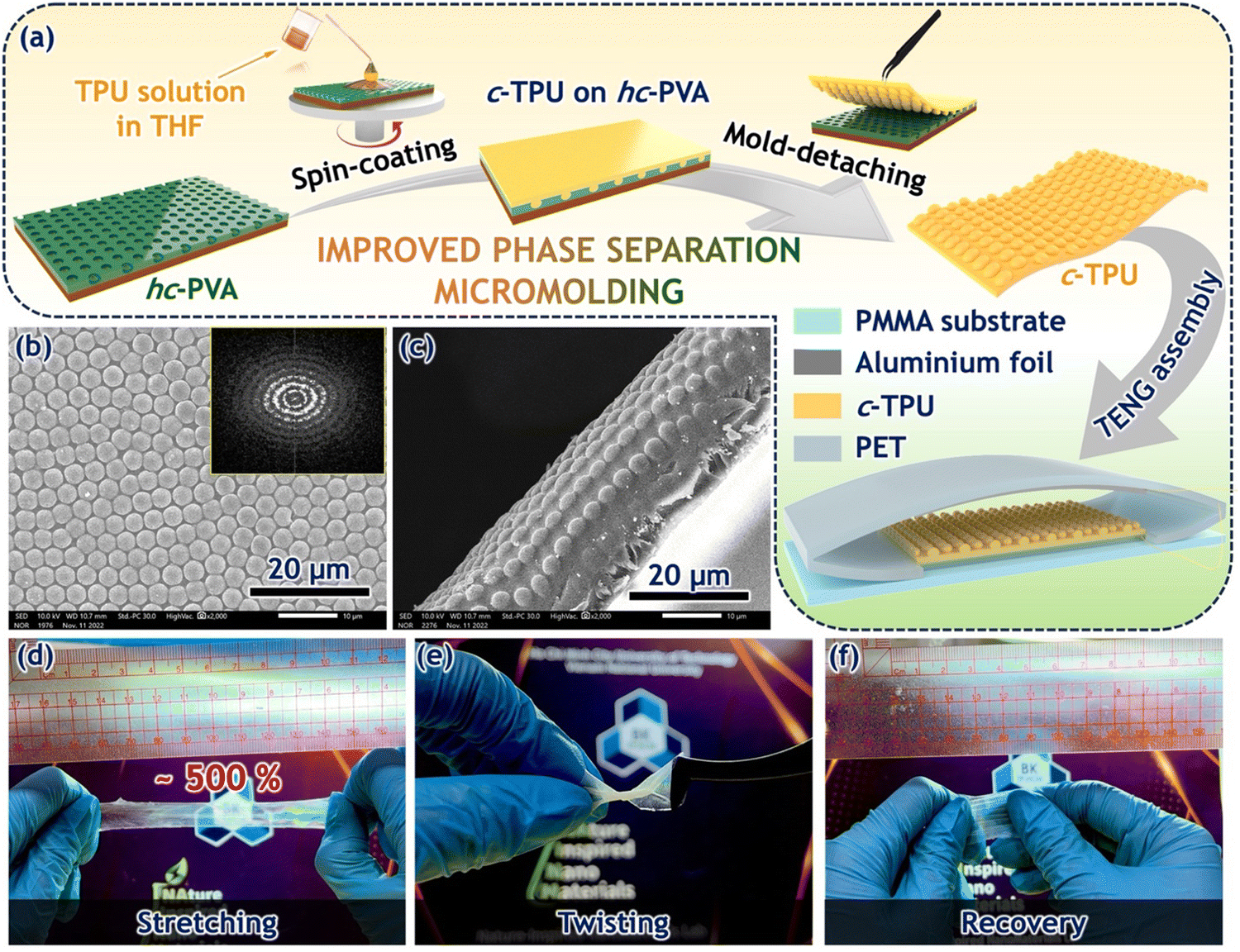 | ||
| Fig. 1 The fabrication process of c-TPU and its outstanding features. (a) Sketching step-by-step fabrication procedure of the c-TPU and TENG device. (b) Surface morphology of microdome patterns with the inset of fast Fourier transform (FFT) pattern. (c) Cross-sectional view of the c-TPU film. (d) Stretchability of c-TPU up to 500%. (e) Twisting ability of c-TPU and recovery after deformation in (f). | ||
Working mechanism of the c-TPU-based triboelectric nanogenerator
The rational design of the portable arch-shaped TENG is showcased in Fig. 1a with the practical prototype illustrated in Fig. 2a. The contacting area is 2.5 cm × 2.5 cm, working based on the contact-separation mode. The open-circuit voltage (VOC) signals of flat and convex TPU are indicated in Fig. 2b, corresponding to each contact-separation state in Fig. 2c. Initially, in a neutral state without any charges, the device, upon experiencing a 30 N push from the vibration shaker, sees its upper aluminum electrode approaching the TPU electret until they make full contact (i). The electron donation and acceptor of the TPU and Al surfaces enable them to become positively charged and negatively charged, respectively thanks to the triboelectrification. Subsequently, the release of the charged surfaces leads to the appearance of electrostatic field, driving the electrons from the top electrode to the bottom one through a load (ii), forming the first current releasing signal until the electrostatic equilibrium is settled (iii). Then, when the two surfaces are reaching each other again (iv), the transferred electrons flow back to the original electrode through the external load and generate an electrical current (contacting signal). The working cycle is completed when they are fully pressed again. These contact-separation states and the electron-donating and accepting abilities are consistent with the previous reports.28,29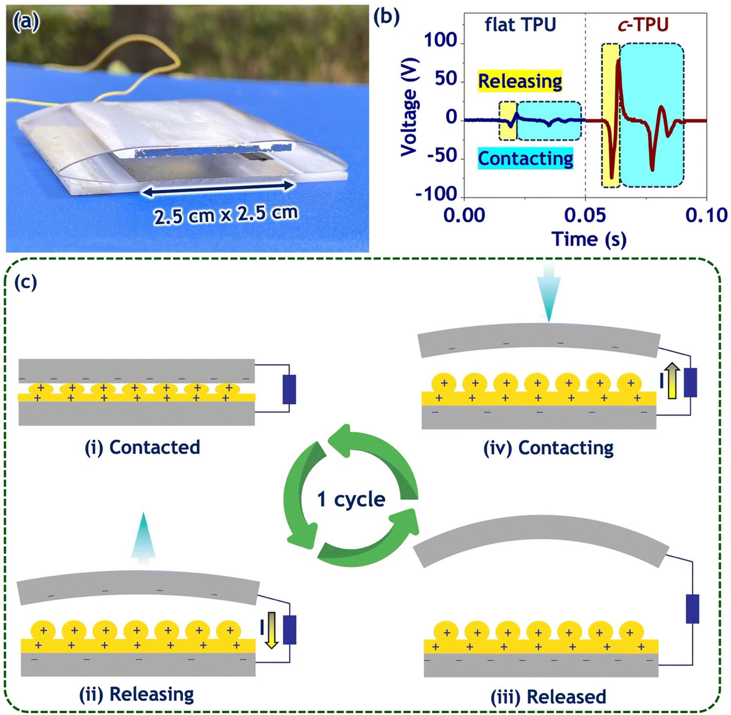 | ||
| Fig. 2 The portable TENG device and its working mechanism. (a) Practical prototype of TENG. (b) Signal of one working cycle with the corresponding states in (c). | ||
COMSOL simulation results
Fig. 3 provides a comprehensive visual comparison of the simulated outputs for both flat and microstructured TPU films. As the two tribosurfaces come into contact (d = 0 mm), no electrical potential appears (Fig. 3a), which is similar in both cases of flat and structured films. After separation, due to the electrostatic induction, the electrical potential gradually increases with the rise in separation distance. At 5 mm distance, the simulated potential of the flat surface was ∼23 kV. The addition of microconvex structure greatly fosters the electric potential to 88.1, 88.5 and 88.7 kV corresponding to the c-TPU_10, c-TPU_15 and c-TPU_20 films (Fig. 3b–e). The trend reveals that the difference in the film features of c-TPU including film thickness and surface pattern resulted in the change in electric potential. Additionally, the far thinner (c-TPU_10) or far thicker (c-TPU_20) films also affect the attained voltage due to the influence on the electrostatic field, as summarized in Fig. 3f.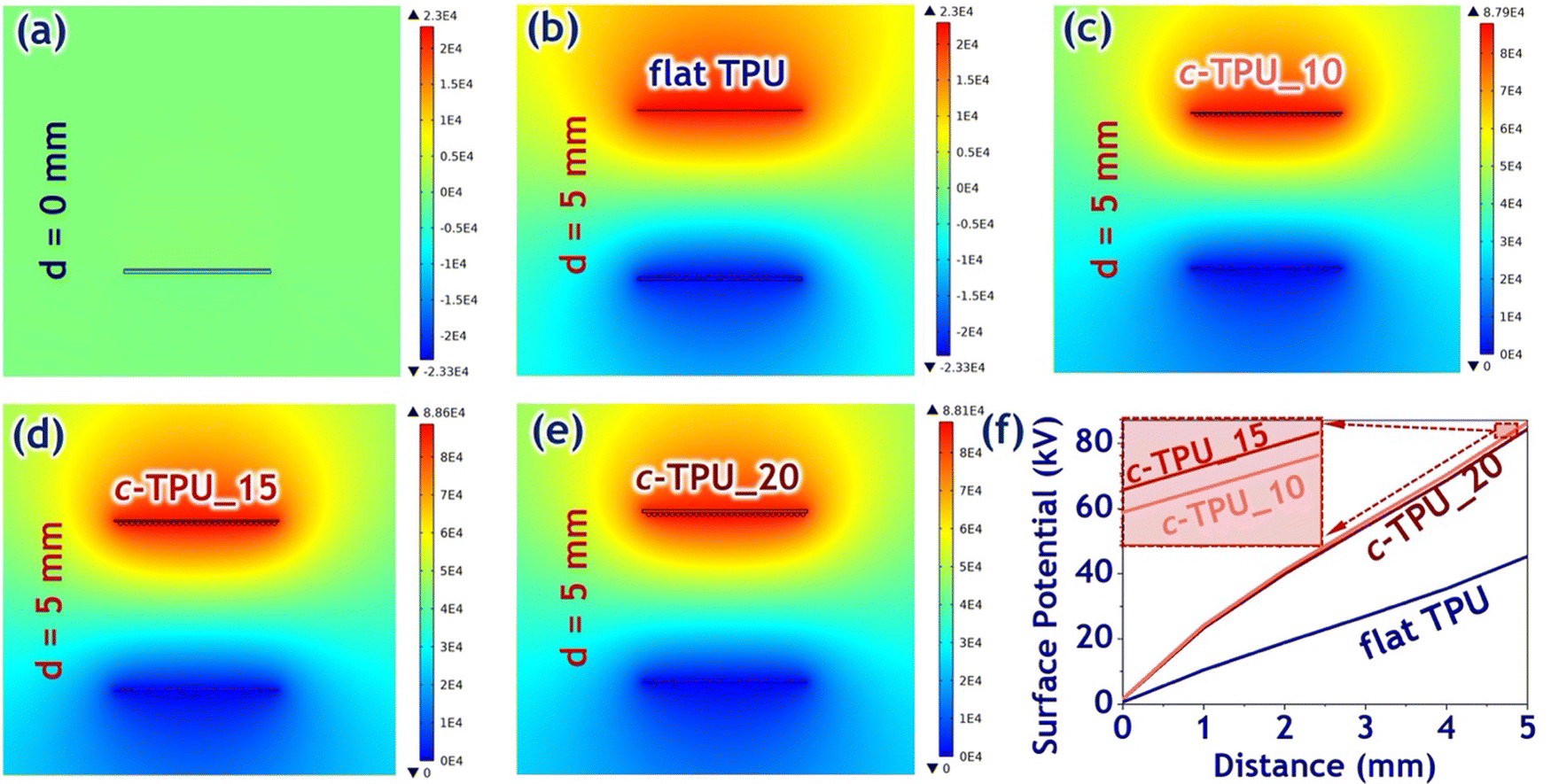 | ||
| Fig. 3 Simulated output results of flat TPU, c-TPU_10, c-TPU_15 and c-TPU_20, respectively. (a) Contacting state with no electric field. (b)–(e) Separating state (distance d = 5 mm) of flat TPU, c-TPU_10, c-TPU_15 and c-TPU_20, respectively. (f) Summarized results at different distances. | ||
Empirical output performance
To verify the simulated output, the c-TPU films fabricated with various concentrations were assembled. With the same mother mold, the difference in the polymer concentration led to distinctive surface patterns and thickness. As can be seen in Fig. 4a, the water contact angle (WCA) value of a flat dense surface is relatively low (82.6°). After surface micropatterning, the hydrophobicity was enhanced dramatically with the highest WCA of over 114.5° of c-TPU_15, slightly higher than those of c-TPU_10 and c-TPU_20. This phenomenon was due to the air voids appearing on the film surface, which was commonly witnessed in previous research.30,31 Based on the WCA results, the surface solid fraction (SSF) can be calculated following the Cassie–Baxter eqn (1):32,33| cosθc = fs(cosθc + 1) − 1 | (1) |
 | ||
| Fig. 4 Film characteristics formed with various TPU concentrations and their corresponding output. (a) Water contact angle (WCA) results and calculated surface solid fraction (SSF) of flat TPU, c-TPU_10, c-TPU_15 and c-TPU_20, respectively. (b) Empirical output voltage signals of TENG composed of flat TPU, c-TPU_10, c-TPU_15, and c-TPU_20 with an inset illustration of practical thickness values. | ||
Along with pattern features, the polymer concentration is also a determining factor of the film thickness, both of which strongly influence the effective surface area and electrostatic induction, directly affecting the output performance of TENGs. Similar to the trend of simulated results, the open-circuit voltage (VOC) of convex-structured film performs much better than flat film. The VOC of TENGs gradually increases with the assembly of c-TPU_10 and c-TPU_15 with the respective thicknesses of 11 and 19 μm. In particular, c-TPU_15 achieved a VOC of 84 V, which was at least 5 times larger compared to 15 V of flat TPU. Then, the VOC tended to reduce at the TPU concentration of 20 wt% because of the incompletely replicating patterns and large film thickness, leaving the VOC of 72 V.
In brief, the outstanding enhancement of VOC was triggered by the convex microstructure on the TPU surface mainly due to the 3 factors: (i) enhanced effective contact surface area; (ii) lateral deformation of convex patterns of elastomeric TPU, which is enabled with all directions due to the spherical shape of microdome; (iii) electron-storing effect of “cubital fossa”, which hinders the electron loss into the air, helping electrons gradually accumulate; (iv) electrification-boosting effectiveness thanks to the “cubital fossa”, enabling the electrification between the curved area on the microdomes and flat area, thereby facilitating the electron transferring inside the TPU film and enhancing the general output (see Fig. S2–S4 in ESI†). This phenomenon was accurately predicted in the simulation section.
The great enhancement in the electrical output of c-TPU in TENG devices was strengthened in Fig. 5 in comparison with flat TPU. Triggering frequency is directly proportional to VOC in all cases (Fig. 5a). Even with a very small vibration frequency of 1 Hz, the c-TPU_15 based TENG could generate VOC of over 50 V while the value of flat TPU is quite low and insignificant (∼5 V). Fig. 5b and c reveal the instantaneous power density and average power density (Paverage) of TPU films, which can be calculated using eqn (2) as follows.
 | (2) |
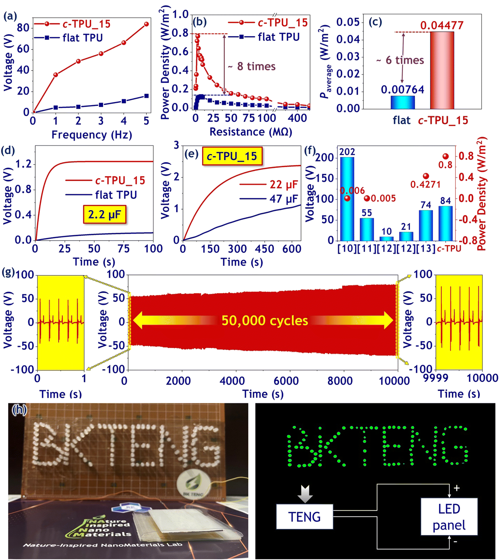 | ||
| Fig. 5 The electrical performance of flat TPU and c-TPU_15, respectively. (a) Effect of triggering frequency on the output voltage. (b) and (c) Instantaneous and average power density of flat TPU and c-TPU_15, respectively. (d) Capacitor-charging ability of flat TPU and c-TPU_15. (e) Large capacitor-charging ability of c-TPU_15. (f) Relation between voltage and power density of c-TPU compared to previous TPU-based studies. (g) Working durability of c-TPU after 50000 cycles. (h) c-TPU lighting up 120 LEDs. | ||
In comparison with previous research using TPU as tribosurfaces, the fabrication of c-TPU shows far more cost-, effort-, and time-savings but the increment overshadows other techniques (Fig. 5f). For instance, K. Zhou et al. presented an advanced TENG using electrospun TPU/silver nanowires/reduced graphene oxide and deploying alternatingly with aluminum electrodes like sandwich performed an electrical output of 202 V and 0.006 W m−2.12 TPU adding carbon black paired with polytetrafluoroethylene could create an output voltage of 55 V and power density of 0.005 W m−2.13 Another research group compared flat with electrospun TPU-based TENGs and concluded that the VOC of flat TPU was 10 V and electrospun TPU was 21 V.14 Most recently, TPU functionalized with polydimethylsiloxane diol and fluorine-contained extender assembled with nylon harvested a voltage of 74 V and power density of 0.4271 W m−2.15 This indicates the tremendous potential of the newly developed microdomes on the electret surface due to the straightforwardness but significantly increasing the output to 84 V and 0.8 W m−2, which was considerably enhanced compared to the previous studies requiring complex equipment and advanced materials. Most strikingly, after a period of working time, c-TPU could not only maintain the high output but also increase the voltage by 50% compared to the original value. This phenomenon demonstrated the high mechanical strength under impact of the TPU, getting rid of the screening effect which commonly occurs in other materials and reducing the output after a few thousand working cycles.34,35 Furthermore, the increase in output voltage even after 50000 cycles of TPU in Fig. 5g can be attributed to the aforementioned electron-storing effect in the “cubital fossa” of microdomes. The c-TPU-based TENG could directly lighten up a BKTENG-shaped panel with over 120 green LEDs even with a small vibration force (see Video S2 in the ESI†).
Practical TENG devices based on c-TPU films
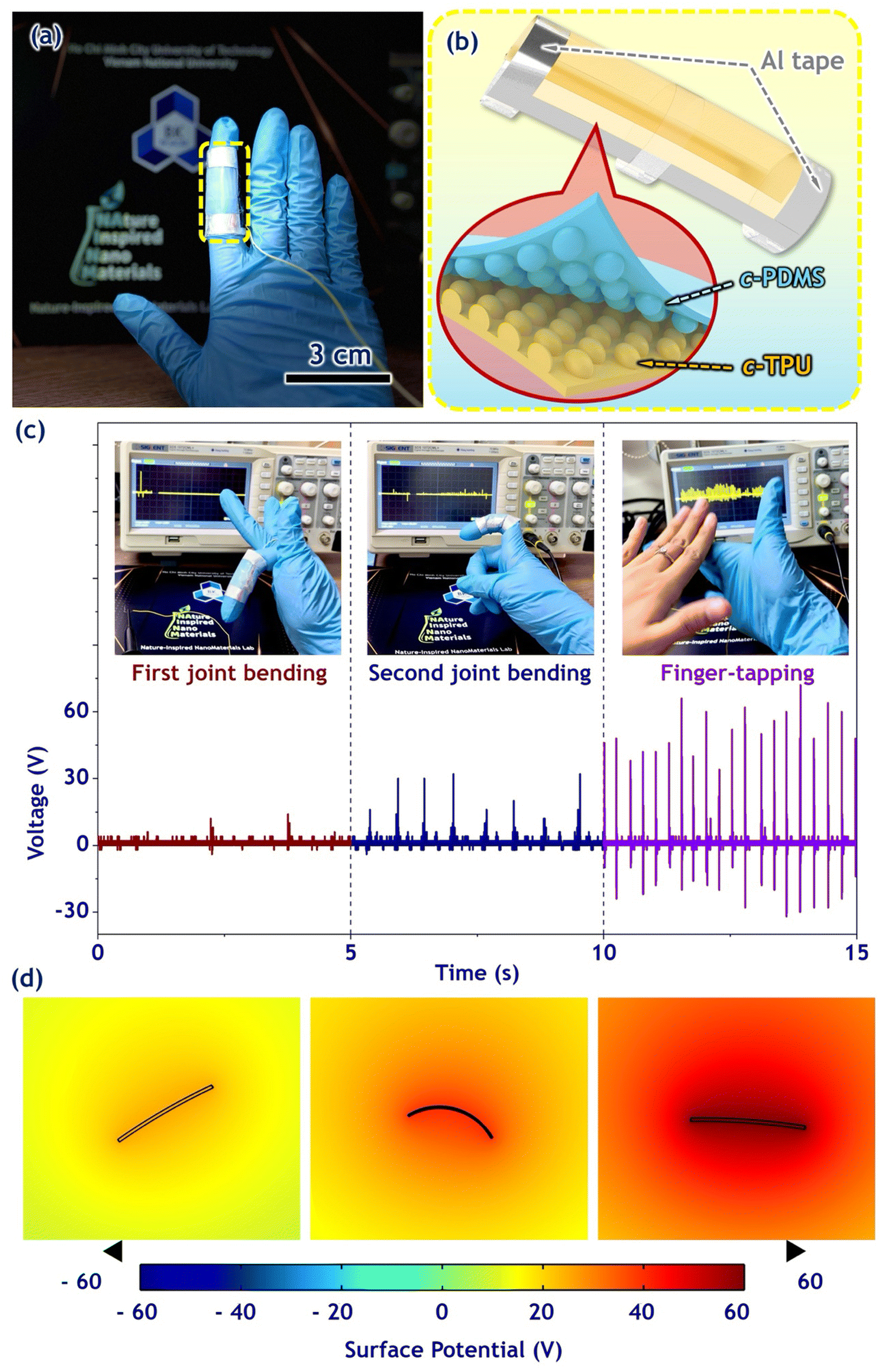 | ||
| Fig. 6 Demonstration of practical finger-motion detecting sensor (FD-sensor). (a) 3D structure of FD-sensor. (b) Practical FD-sensor device. (c) The electrical signal of FD-sensor working under first joint bending, second joint bending and finger-tapping. (d) COMSOL simulated results of FD-TENG. | ||
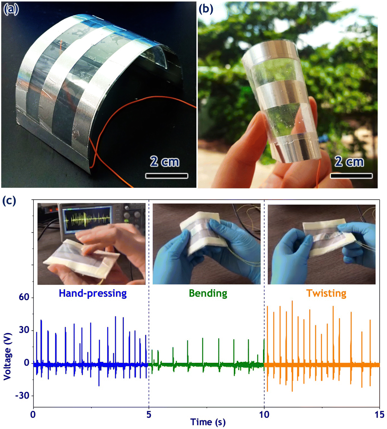 | ||
| Fig. 7 Flexible transparent no-gap TENG device. (a) and (b) Practical image of flexible transparent no-gap TENG device. (c) Output signals of a flexible transparent no-gap TENG device under impacts: hand-pressing, bending, and twisting. | ||
Conclusions
In this study, we have achieved the successful creation of a microdome-pattern array onto thermoplastic polyurethane using the innovative developed improved phase separation micromolding technique. The obtained results indicated the successful creation of a uniformly patterned array, with a pattern size of 3.38 μm and a pattern height of 1.68 μm, across a sample area of 25 cm2. Additionally, the patterned TPU has demonstrated exceptional mechanical strength with an impressive elongation capability of 500%. We also clarified that the imprinting microdome-pattern array on the TPU surface resulted in enhancements in effective surface contact area, lateral deformation, and hydrophobicity, thereby leading to a notable increase in the output performance. In particular, the power density of the triboelectric nanogenerator reached a remarkable value of 0.8 W m−2, which is at least 8 times as high as that of flat TPU. More importantly, c-TPU completely overshadows other materials to be applied as an electret with ultra-high stability even 50000 working cycles. The highly flexible, shape-memorable, and bio-compatible transparent TENG is immensely promising to serve as a highly sensitive finger-motion detection sensor for monitoring hand-arm vibrating syndrome and other related fields requiring online sensing devices.
Author contributions
N. M. Chau: conceptualization, methodology, experimental, investigation, formal analysis, visualization, original draft – writing and editing. P. M. Tran: methodology, experimental, original draft – writing. T. H. Le: demonstration. V.-T. Bui: formal analysis, supervision, funding acquisition. T. T. H. La: formal analysis, supervision, funding acquisition.Conflicts of interest
The authors declare no competing financial interest.Acknowledgements
This research was funded by Vietnam National University HoChiMinh City (VNU-HCM) under grant number 562-2022-20-03. Ngoc Mai Chau was funded by the Master, PhD Scholarship Programme of Vingroup Innovation Foundation (VINIF), code VINIF.2022.TS073 and Kurita Asia Research Grant (22Pvn024-U2). We acknowledge the support of time and facilities from Ho Chi Minh City University of Technology (HCMUT), VNU-HCM for this study.References
- F. R. Fan, Z. Q. Tian and Z. Lin Wang, Nano Energy, 2012, 1, 328–334 CrossRef CAS.
- J. Ahn, J. S. Kim, Y. Jeong, S. Hwang, H. Yoo, Y. Jeong, J. Gu, M. Mahato, J. Ko, S. Jeon, J. H. Ha, H. S. Seo, J. Choi, M. Kang, C. Han, Y. Cho, C. H. Lee, J. H. Jeong, I. K. Oh and I. Park, Adv. Energy Mater., 2022, 12, 1–11 Search PubMed.
- C. Chen, Z. Wen, J. Shi, X. Jian, P. Li, J. T. W. Yeow and X. Sun, Nat. Commun., 2020, 11, 4143 CrossRef CAS PubMed.
- X. Chen, L. Gao, J. Chen, S. Lu, H. Zhou, T. Wang, A. Wang, Z. Zhang, S. Guo, X. Mu, Z. L. Wang and Y. Yang, Nano Energy, 2020, 69, 104440 CrossRef CAS.
- K. Tao, H. Yi, Y. Yang, H. Chang, J. Wu, L. Tang, Z. Yang, N. Wang, L. Hu, Y. Fu, J. Miao and W. Yuan, Nano Energy, 2020, 67, 104197 CrossRef CAS.
- D. Jiang, Z. Fan, H. Wang, M. Xu, G. Chen, Y. Song and Z. L. Wang, ACS Nano, 2020, 14, 15394–15402 CrossRef CAS PubMed.
- P. Cheng, H. Guo, Z. Wen, C. Zhang, X. Yin, X. Li, D. Liu, W. Song, X. Sun, J. Wang and Z. L. Wang, Nano Energy, 2019, 57, 432–439 CrossRef CAS.
- H. Liu, Y. Li, K. Dai, G. Zheng, C. Liu, C. Shen, X. Yan, J. Guo and Z. Guo, J. Mater. Chem. C, 2015, 4, 157–166 RSC.
- M. Zhou, W. Zhu, S. Yu, Y. Tian and K. Zhou, Compos., Part C: Open Access, 2022, 7, 100212 CAS.
- M. Tian, N. Ning, J. Yao, X. Liu, H. Sun, S. Liu, Y. Jiang, B. Yu and L. Zhang, Ind. Eng. Chem. Res., 2021, 60, 4883–4891 CrossRef.
- C. Xu and Y. Hong, Bioact. Mater., 2022, 15, 250–271 CAS.
- K. Zhou, Y. Zhao, X. Sun, Z. Yuan, G. Zheng, K. Dai, L. Mi, C. Pan, C. Liu and C. Shen, Nano Energy, 2020, 70, 104546 CrossRef CAS.
- W. Zhang, Q. Liu, S. Chao, R. Liu, X. Cui, Y. Sun, H. Ouyang and Z. Li, ACS Appl. Mater. Interfaces, 2021, 13, 42966–42976 CrossRef CAS PubMed.
- S. R. Srither, N. R. Dhineshbabu, D. S. Shankar Rao, S. Krishna Prasad, O. Dahlsten and S. Bose, J. Nanosci. Nanotechnol., 2021, 21, 3072–3080 CrossRef CAS.
- H. Joo, S. Gwak, M. H. Lee, H. Park, C. Lee, J. H. Lee, S. A. Han and J. H. Lee, Sustainable Mater. Technol., 2023, 36, e00638 CrossRef CAS.
- L. Jin, J. Tao, R. Bao, L. Sun and C. Pan, Sci. Rep., 2017, 7, 1–6 CrossRef PubMed.
- Y. Xiong, L. Luo, J. Yang, J. Han, Y. Liu, H. Jiao, S. Wu, L. Cheng, Z. Feng, J. Sun, Z. L. Wang and Q. Sun, Nano Energy, 2023, 107, 108137 CrossRef CAS.
- Y. Zeng, H. Xiang, N. Zheng, X. Cao, N. Wang and Z. L. Wang, Nano Energy, 2022, 91, 106601 CrossRef CAS.
- Y. Yang, J. Han, J. Huang, J. Sun, Z. L. Wang, S. Seo and Q. Sun, Adv. Funct. Mater., 2020, 30, 1–10 Search PubMed.
- L. Dhakar, P. Pitchappa, F. E. H. Tay and C. Lee, Nano Energy, 2016, 19, 532–540 CrossRef CAS.
- K. Qin, C. Chen, X. Pu, Q. Tang, W. He, Y. Liu, Q. Zeng, G. Liu, H. Guo and C. Hu, Nano-Micro Lett., 2021, 13, 1–9 CrossRef CAS PubMed.
- S. Shen, X. Xiao, J. Yin, X. Xiao and J. Chen, Small Methods, 2022, 6, 1–13 Search PubMed.
- J. Han, C. Xu, J. Zhang, N. Xu, Y. Xiong, X. Cao, Y. Liang, L. Zheng, J. Sun, J. Zhai, Q. Sun and Z. L. Wang, ACS Nano, 2021, 15, 1597–1607 CrossRef CAS PubMed.
- W. He, M. Sohn, R. Ma and D. J. Kang, Nano Energy, 2020, 78, 105383 CrossRef CAS.
- V. T. Bui, Q. Zhou, J. N. Kim, J. H. Oh, K. W. Han, H. S. Choi, S. W. Kim and I. K. Oh, Adv. Funct. Mater., 2019, 29, 1–10 CrossRef.
- V.-T. Bui, N. M. Chau, D. P. Huynh, N. D. Huynh, D. Choi and H. Nhat Do, ACS Appl. Energy Mater., 2022, 5, 9791–9800 CrossRef CAS.
- V. T. Bui, L. T. Thuy, Q. C. Tran, V. T. Nguyen, V. D. Dao, J. S. Choi and H. S. Choi, Chem. Eng. J., 2017, 320, 561–569 CrossRef CAS.
- H. Zou, Y. Zhang, L. Guo, P. Wang, X. He, G. Dai, H. Zheng, C. Chen, A. C. Wang, C. Xu and Z. L. Wang, Nat. Commun., 2019, 10, 1–9 CrossRef CAS.
- Y. Yang, J. Qian, Y. Dong, M. A. Nikitina, U. Zafari and X. Xiao, Results Eng., 2022, 14, 100482 CrossRef.
- C. Yang, U. Tartaglino and B. N. J. Persson, Phys. Rev. Lett., 2006, 97, 116103 CrossRef CAS PubMed.
- Q. Du, P. Zhou, Y. Pan, X. Qu, L. Liu, H. Yu and J. Hou, Chem. Eng. Sci., 2022, 249, 117327 CrossRef CAS.
- M. Vigdorowitsch, L. E. Tsygankova, V. V. Ostrikov and L. D. Rodionova, Math. Models Methods Appl. Sci., 2022, 45, 11479–11497 CrossRef.
- V. T. Bui, V. D. Dao and H. S. Choi, Polymer, 2016, 101, 184–191 CrossRef CAS.
- S. Niu, S. Wang, L. Lin, Y. Liu, Y. S. Zhou, Y. Hu and Z. L. Wang, Energy Environ. Sci., 2013, 6, 3576–3583 RSC.
- J. Zhao, D. Wang, F. Zhang, Y. Liu, B. Chen, Z. L. Wang, J. Pan, R. Larsson and Y. Shi, ACS Nano, 2021, 15, 11869–11879 CrossRef CAS PubMed.
Footnote |
| † Electronic supplementary information (ESI) available: Video S1 High stretching property of c-TPU (mp4). Video S2 c-TPU based TENG powering 120 LEDs (mov). Video S3 First joint bending signals (mp4). Video S4 Second joint bending signals (mp4). Video S5 Finger-tapping signals (mp4). Video S6 Softly hand-pressing signals (mp4). Video S7 Flexible TENG bending signals (mp4). Video S8 Flexible TENG twisting signals (mp4). See DOI: https://doi.org/10.1039/d3ma00534h |
| This journal is © The Royal Society of Chemistry 2023 |