
 Open Access Article
 This Open Access Article is licensed under a Creative Commons Attribution-Non Commercial 3.0 Unported Licence
Memory characteristics of anthracene-based polyimides in non-volatile resistive memory devices†
Seung-Hyun
Lee‡
a,
Sechang
Park‡
b,
Ju-Young
Choi
a,
Yun-Je
Choi
a,
Hyung Woo
Ji
a,
Hyeyoung
Joung
a,
Dam-Bi
Kim
a,
Kang-Hoon
Yoon
a,
Gyumin
Ji
b,
Daeho
Choi
b,
Jaekang
Lee
b,
Ki-Jung
Paeng
a,
Jaesung
Yang
 a,
Soohaeng
Cho
*b and
Chan-Moon
Chung
*a
a,
Soohaeng
Cho
*b and
Chan-Moon
Chung
*a
aDepartment of Chemistry, Yonsei University, Wonju, Gangwon-do 26493, Republic of Korea. E-mail: cmchung@yonsei.ac.kr
bDepartment of Physics, Yonsei University, Wonju, Gangwon-do 26493, Republic of Korea. E-mail: shcho@yonsei.ac.kr
First published on 13th October 2023
Abstract
Recently, polyimides (PIs) containing the anthracene moiety have been demonstrated to show a wide range of electrical bistable switching behavior, depending on the chemical structures or electrode materials used in the memory devices. There is a need to develop advanced anthracene-containing PIs having higher memory performance. In this study, a new anthracene-containing diamine, 4-(anthracen-9-ylmethoxy)-1,3-diaminobenzene (AMDA), was synthesized, and polymerized with 4,4′-(hexafluoroisopropylidene)diphthalic anhydride (6FDA) to prepare 6FDA-AMDA PI. For comparison, another PI (6FDA-AnDA PI) was prepared from 6FDA and 2,6-diaminoanthracene (AnDA). 6FDA-AMDA PI and 6FDA-AnDA PI have anthracene moieties in the side and main chains, respectively. 6FDA-AMDA PI showed higher solubility in common organic solvents and less tendency of gelation compared to 6FDA-AnDA PI. The prepared PIs exhibited excellent thermal stability. The Al/6FDA-AMDA PI/indium tin oxide (ITO) device showed write-once-read-many times (WORM) behavior with an on/off ratio up to 106, a threshold voltage of 2.40 V, and a high device yield of 80%. In contrast, the Al/6FDA-AnDA PI/ITO device exhibited WORM behavior with an on/off ratio of up to 104, a threshold voltage at 2.50 V and a 20% device yield. The mechanisms associated with the memory effect are explained using density functional theory (DFT) and time-dependent density functional theory (TD-DFT) calculations. The lower switching voltage and higher device yield of 6FDA-AMDA PI may be attributed to more effective inter-chain charge transfer of the side-chain PI, compared to the main chain PI (6FDA-AnDA PI). This study demonstrates that the 6FDA-AMDA PI is suitable as an active material for solution-processable non-volatile memories.
1. Introduction
Over the past few decades, extensive efforts have been devoted to the research of resistive switching memory to meet the demands of next-generation information technology because the resistive switching devices have high storage density, fast operating speed, simple structure and low power consumption.1–9 The resistive switching memory is generally composed of two electrodes separated by a functional isolator. This device can show two or more different ohmic resistances referred to in the simplest case as the high resistance state (HRS) and low resistance state (LRS). The digital information “0” can be defined by the LRS and “1” by the HRS. The information is retrieved by measuring the electrical current, when a small read voltage is applied. The device yield represents the percentage of memory cells that operate stably of tested cells.Various polymer materials have been reported to show electrical resistive switching effects.10–15 Among them polyimides (PIs) have attracted significant attention as an active layer for memory devices due to their many advantages, including outstanding thermal stability, good dimensional stability, excellent processability, and superior electrical properties.16–29 High dimensional thermal stability is required to prevent delamination upon the thermal treatment of the memory devices.30 Regarding processability, the advantage is that devices can be made using simple methods such as spin coating, without using vacuum deposition equipment that is commonly used for memory device research and development. These PIs were designed by introducing electron-donating and electron-accepting groups, which enable device-tailored electronic transitions.5,31 PI structures containing different electron donor and acceptor moieties have been demonstrated to exhibit non-volatile or volatile memory behavior.
Recently, PIs containing an anthracene moiety have been demonstrated to show electrically on and off state bistable switching behavior.32–37 Anthracene-based moieties have been introduced into PIs as a hole-trapping site, forming an efficient electron-donating structure. It is possible to tune the highest occupied molecular orbital (HOMO) energy level and the lowest unoccupied molecular orbital (LUMO) energy level, as well as the charge transfer ability of PIs. In our previous report,36 resistive switching memory devices were fabricated from 4,4′-(hexafluoroisopropylidene)diphthalic anhydride (6FDA)-2,6-diaminoanthracene (AnDA) PI, with an anthracene moiety in the main chain. 6FDA-AnDA poly(amic acid) (PAA) was first prepared by the reaction of 6FDA and AnDA, and then the PAA intermediate was imidized to 6FDA-AnDA PI. However, the 6FDA-AnDA PAA sample had a tendency to undergo gelation even at very low concentration of the PAA, so there was some difficulty to synthesize 6FDA-AnDA PI. In addition, the memory device yield of 6FDA-AnDA was very low (around 20%). In this context, it is necessary to develop an anthracene-containing PI having higher solubility in common solvents and a higher device yield. If an anthracene-containing PI is soluble in common solvents, its processability can be greatly improved because one can have much choice of selection of solvents that are the most suitable for the device fabrication process. It should be noted that, except for our previous literature,36 there have been no reports on the device yields in the research literature on other conventional anthracene-containing PI memory systems without any dielectric additive such as graphene oxide.
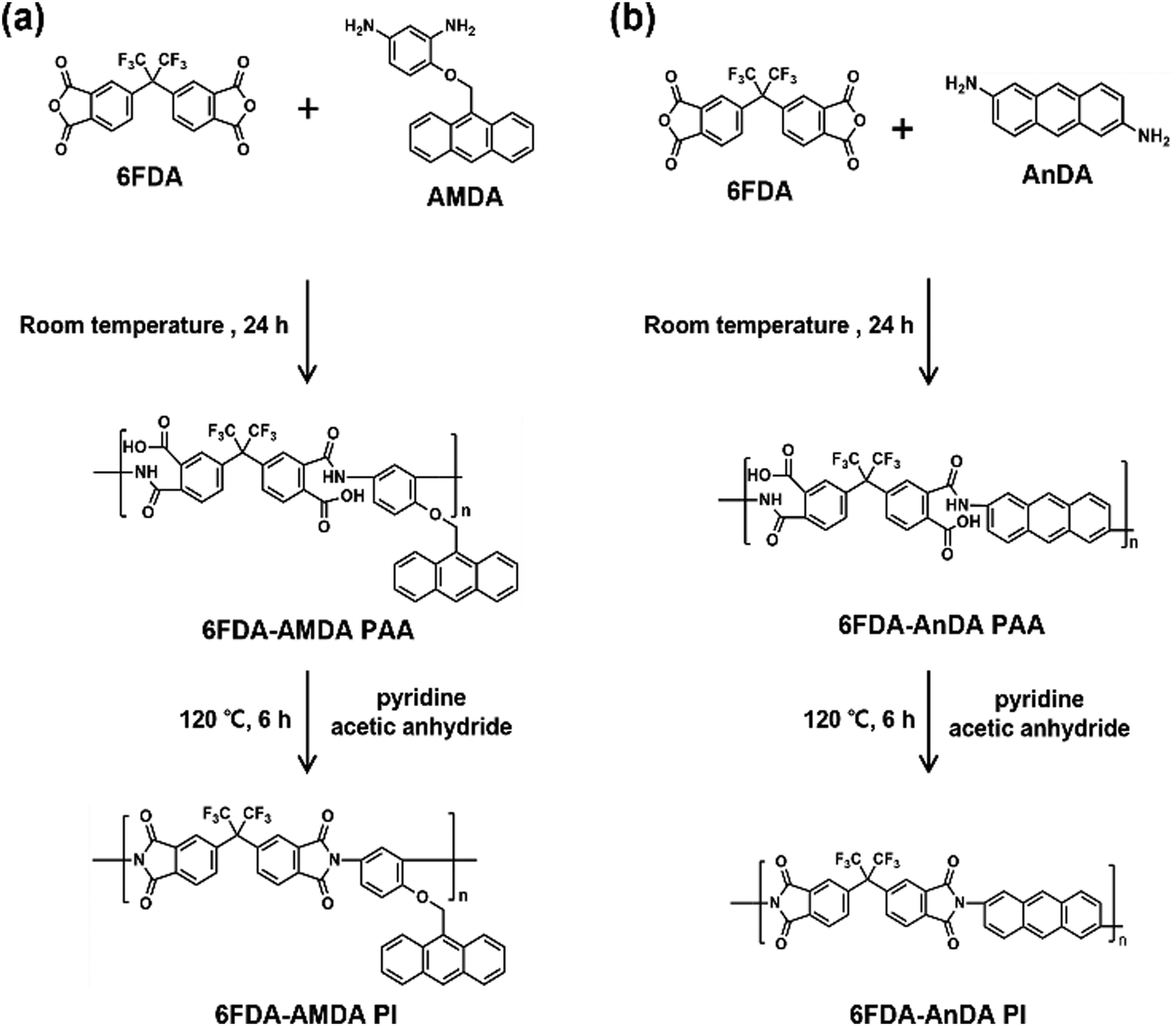
In this paper, we report the synthesis and electronic properties of a new PI containing anthracene moiety. A novel diamine, 4-(anthracen-9-ylmethoxy)-1,3-diaminobenzene (AMDA), was prepared and polymerized with 6FDA. A comparison PI (6FDA-AnDA PI) was also prepared from 6FDA and AnDA. 6FDA-AMDA PI and 6FDA-AnDA PI had anthracene moieties in the side and main chains, respectively. The memory behaviors of the PIs were studied by using a sandwich device configuration of a PI film between Al and ITO electrodes. The results of this study provide a new strategy to design efficient non-volatile resistive memory devices.
2. Experimental section
2.1. Materials
Phthalic anhydride, isoquinoline, 9-anthracenemethanol (AM), diisopropyl azodicarboxylate (DIAD), 6FDA and hydrazine monohydrate were purchased from Sigma-Aldrich. Amidol and triphenylphosphine (TPP) were purchased from Tokyo Chemical Industry Co., Ltd. N,N-Dimethylformamide (DMF), N,N-dimethylacetamide (DMAc), dimethyl sulfoxide (DMSO), N-methyl-2-pyrrolidone (NMP), tetrahydrofuran (THF), chloroform, acetone, ethanol, methanol, methylene chloride (MC), ethyl acetate, acetic anhydride and pyridine were purchased from Duksan Pure Chemicals Co., Ltd, Korea. All the chemicals were used as received without further purification. 2,6-Diaminoanthracene (AnDA) was prepared using a previously reported method.382.2. Instruments
Fourier-transform infrared (FT-IR) spectra were measured with a PerkinElmer Spectrum One B FT-IR spectrometer. 1H and 13C nuclear magnetic resonance (NMR) spectra were recorded on a Bruker 400 MHz spectrometer with the DMSO-d6 solvent. Elemental analysis was performed using a Thermo Fisher Scientific EA 2000 CHN elemental analysis instrument. Gel permeation chromatography (GPC) analysis of the PIs was conducted using a Thermo Fisher Scientific Ultimate 3000 with DMF as the eluent and polystyrene as the standard. The optical properties were measured using a PerkinElmer Lambda 25 UV-Vis spectrometer. Thermogravimetric analysis (TGA) was conducted with a TA instruments Discovery TGA 55 under a nitrogen atmosphere with a balance flow rate of 40 mL min−1 and a furnace flow rate of 60 mL min−1. Differential scanning calorimetry (DSC) analysis was performed on a TA instruments Discovery DSC 25 instrument at a scan rate of 10 °C min−1 in flowing nitrogen gas. Electrochemistry was performed with an Ametek 273A potentiostat/galvanostat. Cyclic voltammetry (CV) was performed by a three-electrode cell, in which indium tin oxide (ITO) was used as a working electrode. A platinum wire was used as an auxiliary electrode and an Ag/AgCl electrode was employed as the reference electrode in a 0.1 M acetonitrile solution of tetrabutylammonium perchlorate (TBAP). Atomic force microscopy (AFM) measurements were performed using a Parks systems NX10 in non-contact mode. Current (I)–voltage (V) characteristics were measured using a Keithley 2634 semiconductor parameter analyzer at room temperature. The voltage was applied to the top electrode, while the bottom electrode was grounded. The measurements were performed using a tungsten tip. The compliance current was set to 0.1 A. Field emission scanning electron microscopy (FE-SEM) was performed using a JSM-7610F Schottky Field emission scanning electron microscope (JEOL, Ltd, Tokyo, Japan) with an acceleration voltage of 15 kV and a working distance in the range of 4.5–5.0 mm.2.3. Monomer synthesis
The synthesis of a new diamine monomer, AMDA, is illustrated in Scheme 1. | ||
| Scheme 1 Synthesis of AMDA. | ||
 | ||
| Fig. 1 (a) 1H NMR spectrum of AMDA; (b) FT-IR spectra of Amidol-DP, Amidol-DP-AM and AMDA. | ||
2.4. Polymer synthesis
6FDA-AMDA PI was synthesized via a two-step procedure (Scheme 2(a)). 6FDA (3.10 g, 0.0070 mol) was added to a solution of AMDA (1.19 g, 0.0070 mol) in DMAc (38 mL), and the mixture was stirred for 24 h at room temperature. A mixture of acetic anhydride (1.30 g) and pyridine (1.00 g) was added to the resultant solution. The reaction mixture was then stirred at 120 °C under a nitrogen atmosphere for 6 h. The resultant polymer solution was poured into water (300 mL) and the formed precipitate was collected by filtration. The resulting PI was washed with methanol (200 mL), and then dried at 100 °C for 24 h under vacuum. The 6FDA-AMDA PI IR (KBr, cm−1) spectroscopy absorption peaks were at 3049, 2932, 1785, 1726, 1363, and 1252 cm−1. The number-averaged molecular weight was![[M with combining macron]](https://www.rsc.org/images/entities/i_char_004d_0304.gif) n = 1.58 × 10⁴ g mol−1, with a molecular weight of w = 2.60 × 10⁴ g mol−1, PDI = 1.67 (established by GPC). 6FDA-AnDA PI was synthesized through a similar procedure except for the use of a different diamine monomer (AnDA) (Scheme 2(b)). The 6FDA-AnDA PI IR (KBr, cm−1): absorption peaks were 3061, 1784, 1729, and 1364 cm−1. n was 1.57 × 10⁴ g mol−1, w = 3.75 × 10⁴ g mol−1 and PDI = 2.38 (GPC).
n = 1.58 × 10⁴ g mol−1, with a molecular weight of w = 2.60 × 10⁴ g mol−1, PDI = 1.67 (established by GPC). 6FDA-AnDA PI was synthesized through a similar procedure except for the use of a different diamine monomer (AnDA) (Scheme 2(b)). The 6FDA-AnDA PI IR (KBr, cm−1): absorption peaks were 3061, 1784, 1729, and 1364 cm−1. n was 1.57 × 10⁴ g mol−1, w = 3.75 × 10⁴ g mol−1 and PDI = 2.38 (GPC).
 | ||
| Scheme 2 The synthesis of (a) 6FDA-AMDA PI and (b) 6FDA-AnDA PI. | ||
2.5. Device fabrication and characterization
The fabrication procedure of the PI-based memory devices is shown in Fig. 2(a). The memory devices had a basic structure of Al/PI/ITO, in which ITO acts as the bottom electrode and Al as the top electrode during the voltage sweep. The ITO glass substrates were cleaned with deionized water, acetone, and isopropyl alcohol in an ultrasonic bath, and then treated with ultraviolet–ozone (UVO).39 The dissolved PI solution (1 wt%) in DMAc was filtered through a 0.45 μm pore size polytetrafluoroethylene (PTFE) membrane syringe filter, spin-coated on top of an ITO glass substrate at a rate of 2500 rpm for 60 s. The residual solvent was removed under vacuum at 80 °C for 1 h. The thickness of the thin film was determined to be around 45–64 nm (Fig. 2(b) and (c)). The Al top electrodes were prepared by thermal evaporation onto the polymer thin film surface through a shadow mask at a pressure of about 10−7 torr via a shadow mask with 800 μm diameter holes and a center to center distance of 2 mm. The size of the mask was 2 × 2 cm2.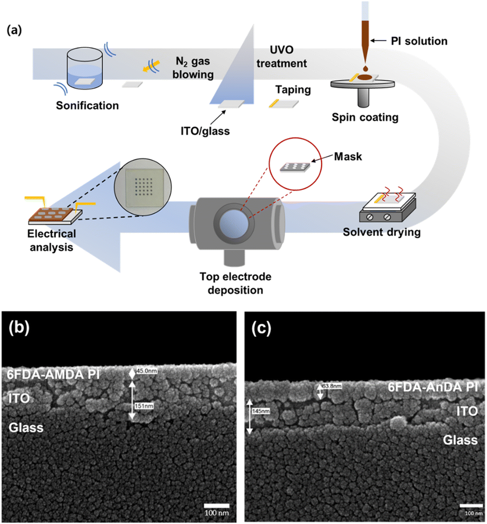 | ||
| Fig. 2 (a) A schematic illustration of the fabrication process of the memory devices, with cross-section SEM images of (b) 6FDA-AMDA PI and (c) 6FDA-AnDA PI coated on ITO glass. | ||
2.6. Molecular simulations
Theoretical molecular simulations were calculated through the Gaussian 09 program package. The optimized gas-phase ground states were calculated using the density functional theory (DFT) method with the B3LYP/6-31G(d) basis set. Electronic transition energies were calculated using time-dependent density functional theory (TD-DFT), using the B3LYP/6-31G(d) basis set.3. Results and discussion
3.1. Synthesis and characterization of monomers
The synthetic path of the new diamine monomer, AMDA, is depicted in Scheme 1. AMDA was synthesized from Amidol through a three-step procedure. First, the two amino groups in Amidol were protected with phthalimido groups to give Amidol-DP. As shown in Fig. 1(b), the FT-IR spectrum of Amidol-DP showed absorption bands at 1765 cm−1 (imide C![[double bond, length as m-dash]](https://www.rsc.org/images/entities/char_e001.gif) O asymmetrical stretching), 1719 cm−1 (imide CO symmetrical stretching), and 1376 cm−1 (imide C–N stretching). The 1H and 13C NMR spectra of Amidol-DP are shown in Fig. S1 and S2 (ESI†), respectively. The signal around 7.8–8.0 ppm in Fig. S1 (ESI†) was assigned to the phthalimido protons of Amidol-DP.
O asymmetrical stretching), 1719 cm−1 (imide CO symmetrical stretching), and 1376 cm−1 (imide C–N stretching). The 1H and 13C NMR spectra of Amidol-DP are shown in Fig. S1 and S2 (ESI†), respectively. The signal around 7.8–8.0 ppm in Fig. S1 (ESI†) was assigned to the phthalimido protons of Amidol-DP.
The anthracene group was incorporated into Amidol-DP using AM via the Mitsunobu reaction.40,41 For the reaction product, the Amidol-DP-AM IR absorption was found at 1247 cm−1 (C–O–C stretching) (Fig. 1(b)). The results of the elemental analysis of Amidol-DP-AM agreed with the calculated values. To obtain AMDA, two phthalic groups in Amidol-DP-AM were removed by hydrolysis with hydrazine monohydrate. The crude product was purified by silica gel chromatography. The 1H NMR spectrum of AMDA is shown in Fig. 1(a): two peaks around 4.2–4.5 ppm were assigned to the amino group protons of AMDA.26 The 13C NMR spectrum of AMDA is shown in Fig. S3 (ESI†). As shown in Fig. 1(b), AMDA showed characteristic bands at 3359 cm−1 and 3405 cm−1 due to N–H stretching.36 In addition, the results of the elemental analysis of AMDA agreed with its calculated values. These results indicate the successful synthesis of AMDA.
3.2. Synthesis and characterization of polyimides
The synthesis of 6FDA-AMDA PI and 6FDA-AnDA PI was accomplished through a two-step procedure (Scheme 2). First, AMDA was polymerized with 6FDA, and the resultant 6FDA-AMDA poly(amic acid) (PAA) was chemically imidized using acetic anhydride and pyridine. The synthesis of 6FDA-AnDA PI was carried out in a similar fashion. As shown in Fig. 3, the FT-IR spectrum of 6FDA-AMDA PI exhibited the characteristic imide absorption bands at 1785 cm−1 (imide CO asymmetric stretching), 1726 cm−1 (imide CO symmetric stretching) and 1363 cm−1 (imide C–N stretching).36 In addition, the broad absorption band at 2400–3400 cm−1 due to the –COOH groups of the precursor (6FDA-AMDA PAA) disappeared. The 6FDA-AnDA PI showed a similar spectroscopic trend.
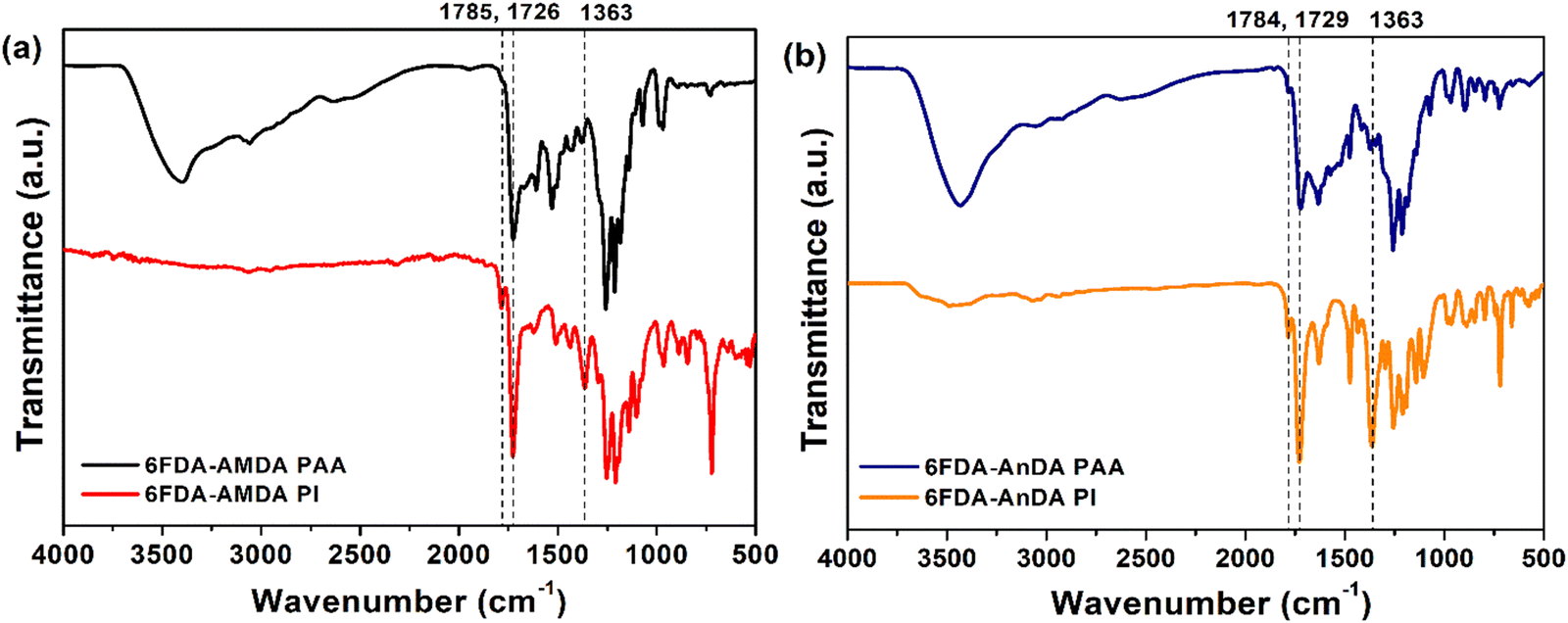 | ||
| Fig. 3 FT-IR spectra of (a) 6FDA-AMDA PAA and PI and (b) 6FDA-AnDA PAA and PI. | ||
The PIs showed n values up to 15![[thin space (1/6-em)]](https://www.rsc.org/images/entities/char_2009.gif) 800 g mol−1 (Table 1) and were soluble in common organic solvents, including NMP, DMF, DMSO, DMAc, and THF (as shown in Table S1 and Fig. S4, ESI†). It was demonstrated that 6FDA-AMDA PI exhibited better solubility and less tendency of gelation compared to 6FDA-AnDA PI. This is probably attributed to the less rigid main chain structure and the presence of a side chain in 6FDA-AMDA PI.42,43
800 g mol−1 (Table 1) and were soluble in common organic solvents, including NMP, DMF, DMSO, DMAc, and THF (as shown in Table S1 and Fig. S4, ESI†). It was demonstrated that 6FDA-AMDA PI exhibited better solubility and less tendency of gelation compared to 6FDA-AnDA PI. This is probably attributed to the less rigid main chain structure and the presence of a side chain in 6FDA-AMDA PI.42,43
| Polymer |
n
(×104) |
w
(×104) |
PDIa (w/n) |
T g (°C) | T 5 (°C) | T 10 (°C) |
|---|---|---|---|---|---|---|
| a Determined through GPC in DMF using polystyrenes as standard. b Measured by DSC from a second heating scan with a heating rate of 10 °C min−1 under N2 atmosphere. c 5% weight loss temperature under N2 atmosphere. d 10% weight loss temperature under N2 atmosphere. | ||||||
| 6FDA-AMDA PI | 1.58 | 2.60 | 1.67 | 374 | 398 | 457 |
| 6FDA-AnDA PI | 1.57 | 3.75 | 2.38 | 358 | 517 | 532 |
It should be noted that the performance of the PI memory devices can be affected by the surface morphology of PIs. The root mean square (RMS) surface roughness values of the 6FDA-AMDA PI and 6FDA-AnDA PI films were 1.10 and 1.08 nm, respectively (Fig. S5, ESI†). These very smooth morphologies are advantageous for memory device performance.44
The thermal stabilities of the prepared PIs were investigated by thermogravimetric analysis (TGA) and differential scanning calorimetry (DSC) under a nitrogen atmosphere (Fig. 4 and Table 1). The 5% weight loss temperatures (T5) of 6FDA-AMDA PI and 6FDA-AnDA PI were 398 °C and 517 °C, respectively, and the 10% weight loss temperatures (T10) of the PIs were 457 °C and 532 °C, respectively. The 6FDA-AMDA PI underwent thermal degradation in a two-step manner. The first weight loss is probably attributed to the degradation of anthracene side groups of the 6FDA-AMDA PI.45 The second degradation process is the degradation of the PI backbones. The DSC curves are displayed in Fig. 4(b). The glass transition temperatures (Tg) of 6FDA-AMDA PI and 6FDA-AnDA PI were 374 °C and 358 °C, respectively. These results indicate that 6FDA-AMDA PI and 6FDA-AnDA PI have very good thermal and dimensional stability up to 350 °C.
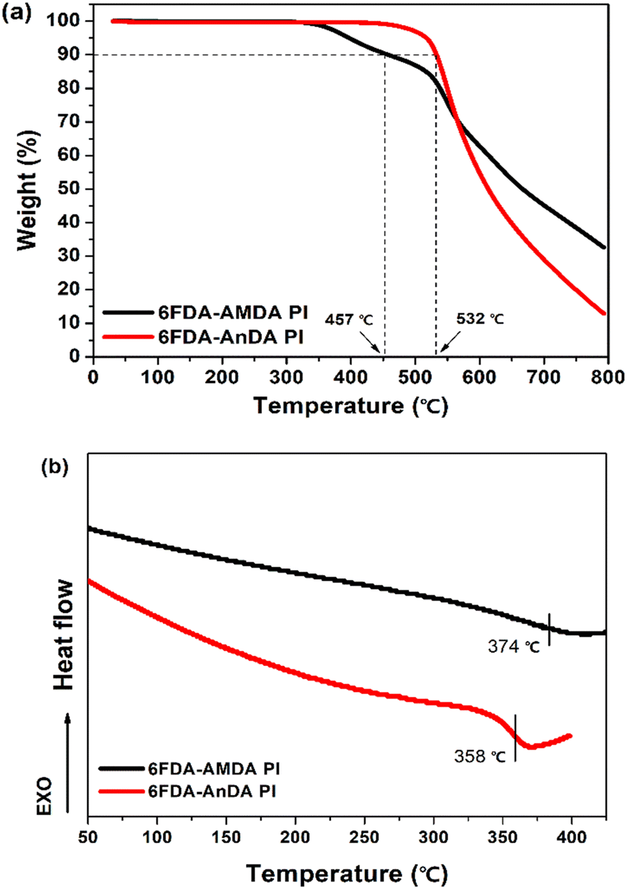 | ||
| Fig. 4 (a) TGA and (b) DSC curves of the PIs. | ||
UV-vis absorption spectra and cyclic voltammetry (CV) diagrams of the PIs were employed to estimate the highest occupied molecular orbital (HOMO) and lowest unoccupied molecular orbital (LUMO) energy levels of the PIs (Fig. 5).24,32 The optical and electrochemical properties are summarized in Table 2. The absorption edges (λonset) of 6FDA-AMDA PI and 6FDA-AnDA PI were 400 nm and 417 nm, respectively (Fig. 5(a)).
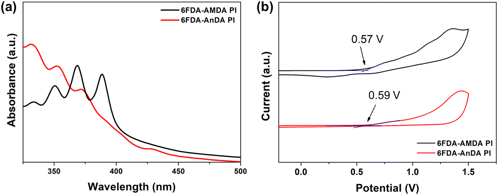 | ||
| Fig. 5 The (a) UV-vis absorption spectra of PIs coated on a quartz substrate and (b) CV diagrams of PIs on an ITO-coated glass substrate. | ||
| Polymer | λ onset (nm) | E g (eV) | E ox (eV) | HOMOd (eV) | LUMOe (eV) |
|---|---|---|---|---|---|
| a Onset wavelength. b Energy gap values estimated using the equation Eg = 1240/λonset (eV). c Oxidation potential. d Estimated using the equation HOMO = −[(Eox(onset) − E(ferrocene) + 4.8)] (eV). e Estimated using the equation LUMO = HOMO + Eg (eV). | |||||
| 6FDA-AMDA PI | 400 | 3.10 | 0.57 | −4.96 | −1.86 |
| 6FDA-AnDA PI | 417 | 2.97 | 0.59 | −4.98 | −2.01 |
The electrochemical analysis of PIs was conducted by cyclic voltammetry using PI thin films spin coated on ITO glass as a working electrode. From the CV diagrams (Fig. 5(b)), the oxidation onset potentials (Eox) of 6FDA-AMDA PI and 6FDA-AnDA PI were determined to be 0.57 V and 0.59 V vs. the Ag/AgCl electrode, respectively. The external ferrocene/ferrocenium (Fc/Fc+) redox standard potential (E1/2) was determined to be 0.41 eV vs. the Ag/AgCl electrode in acetonitrile. The absolute energy level of ferrocene (4.8 eV) below the zero vacuum level was used as the calibration ref. 46. Therefore, the HOMO levels of the 6FDA-AMDA PI and 6FDA-AnDA PI were calculated to be −4.96 eV and −4.98 eV. From the HOMO level and band gaps, the LUMO level was estimated to be −1.86 eV for 6FDA-AMDA PI and −2.01 eV for 6FDA-AnDA PI. The differences between the HOMO/LUMO levels and the band gaps of the 6FDA-AMDA PI and 6FDA-AnDA PI can be attributed to the differences in the polymer structure.
3.3. Memory device characteristics
The memory devices were fabricated using each PI as an active layer (Fig. 2(a)). The fabricated memory devices had a structure of Al/PI/ITO, in which ITO acts as the bottom electrode and Al as the top electrode. After a dissolved PI solution in DMAc was spin-coated on top of an ITO glass substrate, circular Al top electrodes were prepared by thermal evaporation through a shadow mask. The thickness of the thin film was determined to be 45–64 nm. The cross-sectional SEM images of the PIs coated on ITO glasses are shown in Fig. 2(b) and (c).The electrical properties of the memory devices were investigated by carrying out I–V measurements (Fig. 6). Fig. 6(a) and (b) show representative I–V characteristic curves of the memory devices with a compliance current of 0.01 A. The devices of Al/6FDA-AMDA PI/ITO first stayed in the high resistance state (HRS) (i.e., in the off state at a smaller bias). During the first sweep, the current increases abruptly at 2.40 V, indicating transition from an off to on state. After the devices have reached the low resistance state (LRS), i.e., the on state, the conduction state could remain even during the forward and reverse voltage sweep (sweep 500) with a compliance current, 0.01 A or power off. The 6FDA-AMDA PI memory device had a high yield of 80%, with successful outcomes in 20 out of 25 point cells. The yield of the 6FDA-AMDA PI device was much higher than that of the 6FDA-AnDA PI device (with a yield of 20%).
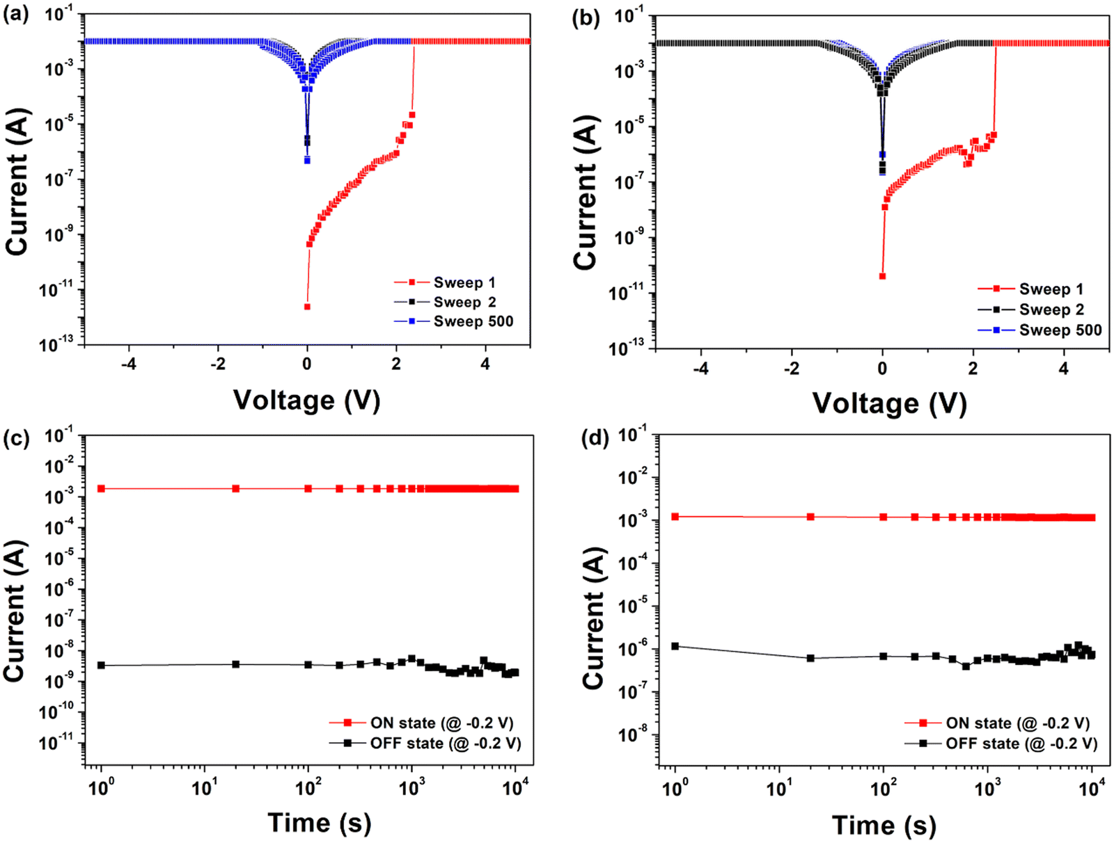 | ||
| Fig. 6 The current–voltage (I–V) characteristics of (a) Al/6FDA-AMDA PI/ITO and (b) Al/6FDA-AnDA PI/ITO memory devices. The retention time tests of both the on and off states of (c) Al/6FDA-AMDA PI/ITO and (d) Al/6FDA-AnDA PI/ITO memory devices under a constant stress of 0.2 V at room temperature. | ||
All devices exhibited WORM memory behavior with an on/off current ratio of about 106 for 6FDA-AMDA PI and about 104 for 6FDA-AnDA PI at a 0.2 V read voltage. In Fig. 6(c) and (d), the retention times and stress tests of both the on and off states of all devices are shown. The 6FDA-AMDA PI device maintained both an on state and off state without degradation for at least 104 s under a constant stress of −0.2 V. Also, the 6FDA-AnDA PI device maintained the on state without degradation for at least 104 s under a constant stress of −0.2 V (Fig. 6(d)). Then, the off state is kept for around 104 s without obvious degradation. All devices demonstrate outstanding irreversible WORM performance.
3.4. Mechanism of the memory devices
To investigate the switching mechanism of the memory devices, the measured I–V data was analyzed using the space charge limited conduction (SCLC; I ∼ Vn+1 (n > 1)) model.47 The SCLC model was analyzed using a logarithmic plot of the I–V data for the off state. Fig. 7 shows the logI–logV curves of the Al/6FDA-AMDA PI/ITO device for the off state. In the region of positive HRS below 0.77 V, the conduction state was characterized by Ohmic conduction (slope = 1.02). This phenomenon occurred due to the thermal carriers at the interface between the 6FDA-AMDA PI and Al.36 In the range of 0.77 V to 2.40 V, the I–V slope of the fitting line was 3.72 in the positive HRS. This indicates that the SCLC mechanism is dominant in the off state. When the applied voltage exceeds 2.40 V, the device exhibited a transition from the off state to on state. The carriers were injected from the electrode to the active layer, overcoming the energy barrier and flowing through the device following the Ohmic conduction.47 With increases in the applied voltage, the generated charge carriers near the electrode lead to an accumulation of space charges. The individual charge carriers undergo electrostatic repulsion, and can inhibit further charge injection to the active layer, which led to an SCLC. Then, an abrupt increase of the current value emerged when the threshold voltage was reached. The anthracene moieties, trifluoromethyl groups, and imide rings might act as the trapping sites in the PI structure.45
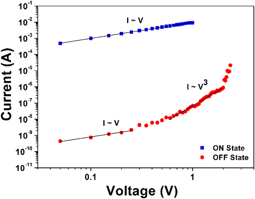 | ||
| Fig. 7 The experimental and fitted I–V curves of the Al/6FDA-AMDA PI/ITO memory device in the on and off states. | ||
Fig. 8 shows the HOMO and LUMO levels of the PIs and the work functions of electrodes determined from UV-vis spectra and CV diagrams. For all the PIs, the energy barrier for the hole injection from ITO to HOMO (0.16 and 0.18 eV) was lower than the electron injection from Al to LUMO (2.42 and 2.27 eV). Therefore, the hole injection from the ITO electrode was much easier than the electron injection from the Al electrode. The results show that the PIs are p-type materials, which means the hole transfer process is dominant.27,44
 | ||
| Fig. 8 The HOMO and LUMO energy levels for the PIs along with the work functions of the electrodes. | ||
To gain insight into the field-induced switching behavior of the memory devices based on the PI active layer, the electronic properties were studied by DFT calculation. Calculations of the optimized geometry and molecular orbitals of the basic unit were carried out using the B3LYP/6-31G(d) level with the Gaussian09 program package. The electronic transition mechanism of PIs can be explained as field-induced charge transfer between the diamine (AMDA or AnDA) and 6FDA monomer units.27,45 In Fig. 9, the HOMO level is located on the donor (diamine units), and the LUMOs are located on the acceptor (dianhydride units). In the PIs, AMDA and AnDA act as electron donors, while 6FDA acts as an electron acceptor to promote the charge transfer complex formation.48 At the threshold voltages of 6FDA-AMDA PI and 6FDA-AnDA PI, the holes of the HOMO level were excited to the LUMO+4 (3.15 eV) and LUMO+2 (3.11 eV) levels, respectively. The excited states of the PIs promote the inter-/intra-molecular charge transfer processes. The charge transfer can occur to form a conductive complex, including from the LUMO+4 and LUMO+2 levels of the donor to the LUMOs of the acceptor.27 Each device may show switching at 3.15 V or 3.11 V, but the devices actually showed switching at 2.40 V (6FDA-AMDA PI) and 2.50 V (6FDA-AnDA PI). The decrease in the switching voltage to the on state may be due to the intermolecular charge transfer between the PI chains. It may be predicted that 6FDA-AMDA PI has more efficient intermolecular charge transfer due to flexible anthracene side chains, compared to 6FDA-AnDA PI having the rigid anthracene main chains. Furthermore, the much higher device yield of 6FDA-AMDA PI (80%) than 6FDA-AnDA PI (20%) might partly be due to the increased intermolecular charge transfer. The stability of the charge transfer complex is related to the recombination abilities of holes and electrons.49 The –CF3 group of 6FDA has the strongest electron-withdrawing ability and the anthracene moiety has higher electron donor power. The 6FDA and diamines containing the anthracene moiety form a stable charge transfer complex through the imide ring. Thus, the stable charge transfer state of PIs can exhibit non-volatile WORM behavior.
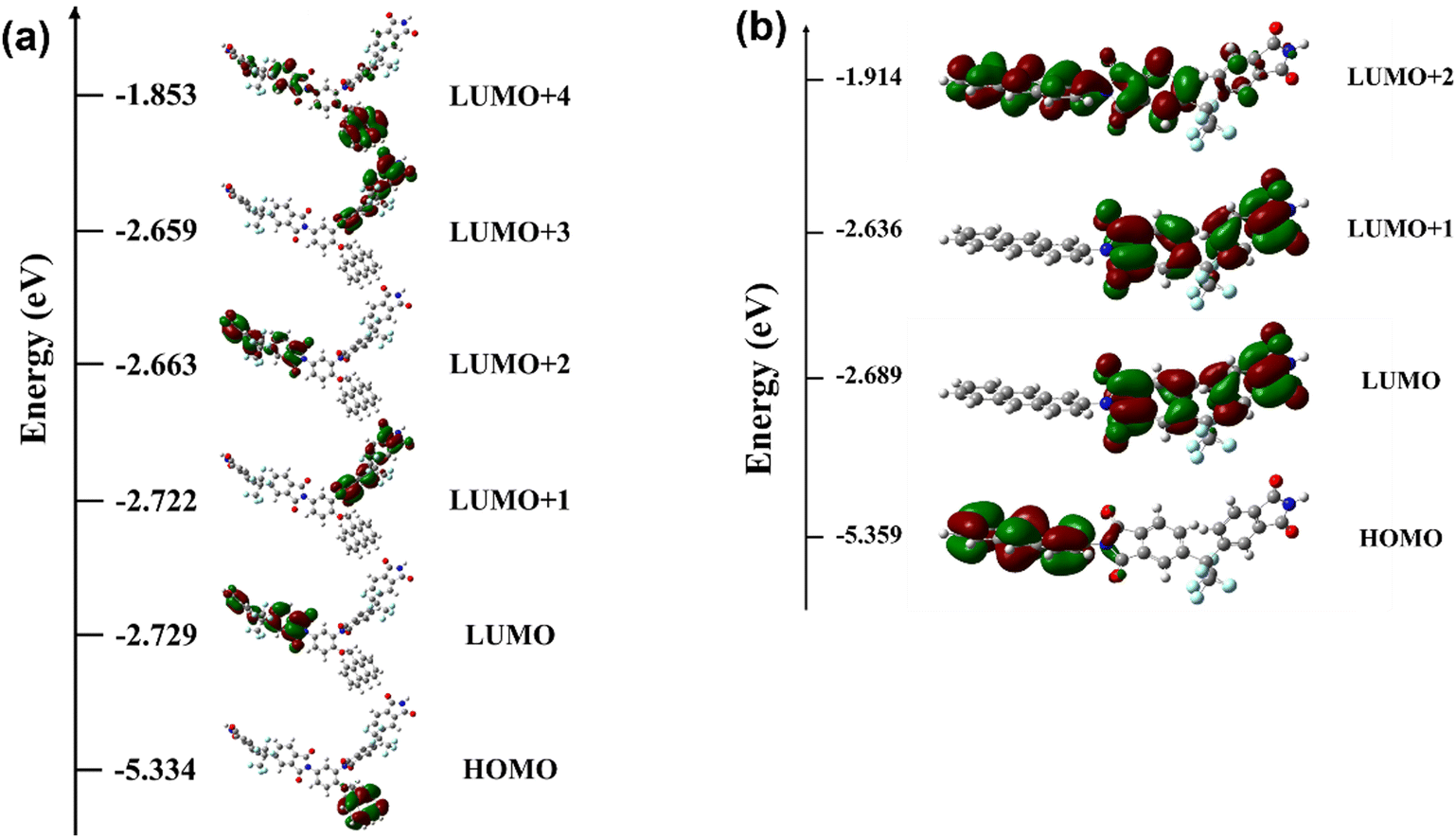 | ||
| Fig. 9 The calculated frontier molecular orbitals of the basic units of (a) 6FDA-AMDA PI (6FDA-AMDA-6FDA) and (b) 6FDA-AnDA PI (AnDA-6FDA). | ||
In the DFT-optimized structure of the 6FDA-AMDA-6FDA, the spacing between the AMDA moiety and the two 6FDA moieties was 14.4 and 8.6 Å. Given these distances between the electron donor and acceptor, a charge transfer process is shown to occur from the AMDA (donor) to one of the two 6FDA (acceptor) in the same PI chain, as is evident from Fig. 9. In a thin film in which a vast number of PI chains are closely packed, the degree of structural heterogeneity in terms of the distance and relative orientation between neighboring AMDA and 6FDA moieties irrespective of whether they belong to a single chain or not is excessively high. Hence it is difficult to model an appropriate system to perform DFT calculations, preventing us from validating if charge transfer between different chains happens. Nevertheless, as we can assume a high degree of chain packing in a thin film state, we conjecture that charge transfer across chains may also occur in addition to that along a single chain although we are unable to say which processes occur preferentially.
4. Conclusions
A new anthracene-containing diamine, AMDA, was synthesized and polymerized with 6FDA. The functional PIs containing the anthracene moiety, 6FDA-AMDA PI (as a side chain) and 6FDA-AnDA PI (as a main chain), were synthesized by chemical imidization of the corresponding precursor PAAs. 6FDA-AMDA PI showed higher solubility in common organic solvents and less tendency of gelation compared to 6FDA-AnDA PI. The PIs showed high thermal stability. The 6FDA-AMDA PI and 6FDA-AnDA PI formed thin films having smooth surface morphologies that enable good memory performance. The 6FDA-AMDA PI and 6FDA-AnDA PI memory devices with a configuration of Al/PI/ITO exhibited non-volatile WORM behavior with on/off ratios up to 106 and 104, switching voltages at 2.40 and 2.50 V, and device yields of 80% and 20%, respectively. The 6FDA-AMDA PI showed a lower switching voltage and higher device yield, which may be derived from more efficient inter-chain charge transfer, as the flexible side-chain-containing PI may have more effective charge transfer than the rigid main-chain PI. The charge transfer and SCLC were proposed to explain the memory mechanism. The off state of the Al/6FDA-AMDA PI/ITO device is found to be governed by Ohmic conduction and the SCLC mechanism. This study presents a strategy for application in commercial memory devices using both the linear and branched anthracene moieties.Author contributions
Conceptualization, S.-H. Lee, S. Park, J.-Y. Choi, S. Cho and C.-M. Chung; formal analysis, H.-W. Ji, H. Joung, D.-B. Kim, K.-H. Yoon, D. Choi, J. Lee, G. Ji, K.-J. Paeng J. Yang; methodology, S.-H. Lee and S. Park; project administration, Y.-J. Choi; supervision, S. Cho and C.-M. chung; writing – original draft, S.-H. Lee and S. Park; writing – review & editing, S. Cho and C.-M. Chung.Conflicts of interest
There are no conflicts to declare.Acknowledgements
This research was supported by the Basic Science Research Program through the National Research Foundation of Korea (NRF) funded by the Ministry of Education (grant no. NRF-2022R1F1A1073236).References
- S. Slesazeck and T. Mikolajick, Nanotechnology, 2019, 30, 352003 CrossRef CAS PubMed.
- G. U. Kamble, A. P. Patil, R. K. Kamat, J. H. Kim and T. D. Dongale, ACS Appl. Electron. Mater., 2023, 5, 2454–2481 CrossRef CAS.
- M. H. Lee and C. S. Hwang, Nanoscale, 2011, 3, 490–502 RSC.
- S. Munjal and N. Khare, J. Phys. D: Appl. Phys., 2019, 52, 433002 CrossRef CAS.
- S. Gao, X. Yi, J. Shang, G. Liu and R.-W. Li, Chem. Soc. Rev., 2019, 48, 1531–1565 RSC.
- F. Zahoor, T. Z. A. Zulkifli and F. A. Khanday, Nanoscale Res. Lett., 2020, 15, 1–26 CrossRef PubMed.
- B. Cho, S. Song, Y. Ji, T. W. Kim and T. Lee, Adv. Funct. Mater., 2011, 21, 2806–2829 CrossRef CAS.
- Y. Tian, S. Zhu, Y. Di, H. Liu, H. Yao, Y. Zhang and S. Guan, Dyes Pigm., 2021, 186, 109020 CrossRef CAS.
- C. Kugeler, M. Meier, R. Rosezin, S. Gilles and R. Waser, Solid-State Electron., 2009, 53, 1287–1292 CrossRef.
- F. Paul and S. Paul, Small, 2022, 18, 2106442 CrossRef CAS PubMed.
- Z. Shen, C. Zhao, Y. Qi, W. Xu, Y. Liu, I. Z. Mitrovic, L. Yang and C. Zhao, Nanomaterials, 2020, 10, 1437 CrossRef CAS PubMed.
- W.-P. Lin, S.-J. Liu, T. Gong, Q. Zhao and W. Huang, Adv. Mater., 2014, 26, 570–606 CrossRef CAS PubMed.
- T. Shi, R. Wang, Z. Wu, Y. Sun, J. An and Q. Liu, Small Struct., 2021, 2, 2000109 CrossRef.
- M. A. U. Khalid, S. W. Kim, J. Lee, A. M. Soomro, M. M. Rehman, B.-G. Lee and K. H. Choi, Polymer, 2020, 189, 122183 CrossRef.
- J. Ali, M. M. Rehman, G. U. Siddiqui, S. Aziz and K. H. Choi, Phys. B, 2018, 531, 223–229 CrossRef CAS.
- C.-J. Chen, H.-J. Yen, W.-C. Chen and G.-S. Liou, J. Mater. Chem., 2012, 22, 14085–14093 RSC.
- Y. Yang, J. Xia, Z. Ding, Y. Zheng, S. Ding and Y. Shen, Eur. Polym. J., 2018, 108, 85–97 CrossRef CAS.
- L. Qu, S. Huang, Y. Zhang, Z. Chi, S. Liu, X. Chen and J. Xu, J. Mater. Chem. C, 2017, 5, 6457–6466 RSC.
- D. Chatterjee, U. A. Jadhav, B. H. Javaegowda, T. D. Dongale, P. S. Patil and P. P. Wadgaonkar, Eur. Polym. J., 2021, 147, 110327 CrossRef CAS.
- J. Nan, Y. Fan, K. Hu, Y. Gao, F. Chen, Y. Shen and Y. Yang, High Perform. Polym., 2022, 34, 1048–1057 CrossRef CAS.
- Y.-C. Chiang, S. Kobayashi, T. Isono, C.-C. Shih, T. Shingu, C.-C. Hung, S.-C. Hsieh, S.-H. Tung, T. Satoh and W.-C. Chen, Polym. Chem., 2019, 10, 5452 RSC.
- A.-D. Yu, T. Kurosawa, Y.-H. Chou, K. Aoyagi, Y. Shoji, T. Higashihara, M. Ueda, C.-L. Liu and W.-C. Chen, ACS Appl. Mater. Interfaces, 2013, 5, 4921–4949 CrossRef CAS PubMed.
- K. Kim, S. Park, S. G. Hahm, T. J. Lee, D. M. Kim, J. C. Kim, W. Kwon, Y.-G. Ko and M. Ree, J. Phys. Chem. B, 2009, 113, 9143–9150 CrossRef CAS.
- L.-C. Hsu, C.-C. Shih, H.-C. Hsieh, Y.-C. Chiang, P.-H. Wu, C.-C. Chueh and W.-C. Chen, Polym. Chem., 2018, 9, 5145–5154 RSC.
- T. Kurosawa, T. Higashihara and M. Ueda, Polym. Chem., 2013, 4, 16–30 RSC.
- S. Park, K. Kim, J. C. Kim, W. Kwon, D. M. Kim and M. Ree, Polymer, 2011, 52, 2170–2179 CrossRef CAS.
- Y. Yang, H. Lu, J. Liu and Y. Shen, Eur. Polym. J., 2018, 108, 10–19 CrossRef CAS.
- J. Zhao, L. Peng, Y.-L. Zhu, A.-M. Zheng and Y.-Z. Shen, Polym. Chem., 2016, 7, 1765–1772 RSC.
- L. Shi, G. Tian, H. Ye, S. Qi and D. Wu, Polymer, 2014, 55, 1150–1159 CrossRef CAS.
- J.-Y. Gao, C.-K. Chen, Y.-C. Lin, C.-C. Kuo and W.-C. Chen, Macromol. Mater. Eng., 2021, 306, 2100512 CrossRef CAS.
- H.-J. Yen and G.-S. Liou, Polym. J., 2016, 48, 117–138 CrossRef CAS.
- S. Park, K. Kim, D. M. Kim, W. Kwon, J. Choi and M. Ree, ACS Appl. Mater. Interfaces, 2011, 3, 765–773 CrossRef CAS PubMed.
- H.-C. Yu, M. Y. Kim, M. Hong, K. Nam, J.-Y. Choi, K.-H. Lee, K. K. Baeck, K.-K. Kim, S. Cho and C.-M. Chung, Electron. Mater. Lett., 2017, 13, 1–8 CrossRef CAS.
- J.-Y. Choi, H.-C. Yu, J. Lee, J. Jeon, J. Im, J. Jang, S.-W. Jin, K.-K. Kim, S. Cho and C.-M. Chung, Polymers, 2018, 10, 901 CrossRef PubMed.
- N. Jia, S. Qi, G. Tian, X. Wang and D. Wu, J. Phys. Chem. C, 2016, 120, 26217–26224 CrossRef CAS.
- J.-Y. Choi, J. Lee, J. Jeon, J. Im, J. Jang, S.-W. Jin, H. Joung, H.-C. Yu, K.-N. Nam, H.-J. Park, D.-M. Kim, I.-H. Song, J. Yang, S. Cho and C.-M. Chung, Polym. Chem., 2020, 11, 7685–7695 RSC.
- H.-C. Yu, M.-Y. Kim, J.-S. Lee, K.-H. Lee, K.-K. Baeck, K.-K. Kim, S. Cho and C.-M. Chung, J. Polym. Sci., Part A: Polym. Chem., 2016, 54, 918–925 CrossRef CAS.
- R. Kantam, R. Holland, B. P. Khanna and K. D. Revell, Tetrahedron Lett., 2011, 52, 5083–5085 CrossRef CAS.
- S. Y. Kim, J.-L. Lee, K.-B. Kim and Y.-H. Tak, J. Appl. Phys., 2004, 95, 2560–2563 CrossRef CAS.
- Y.-J. Shi, D. L. Hughes and J. M. McNamara, Tetrahedron Lett., 2003, 44, 3609–3611 CrossRef CAS.
- K. K. Swamy, N. B. Kumar, E. Balaraman and K. P. Kumar, Chem. Rev., 2009, 109, 2551–2651 CrossRef CAS PubMed.
- L. Yi, W. Huang and D. Yan, J. Polym. Sci., Part A: Polym. Chem., 2017, 55, 533–559 CrossRef CAS.
- Y. Li, H. Xu, X. Tao, K. Qian, S. Fu, Y. Shen and S. Ding, J. Mater. Chem., 2011, 21, 1810–1821 RSC.
- Y. Tian, Y. Song, H. Yao, H. Yu, H. Tan, N. Song, K. Shi, B. Zhang, S. Zhu and S. Guan, Dyes Pigm., 2019, 163, 190–196 CrossRef CAS.
- S. Xia, Z. Sun, L. Yi and Y. Wang, RSC Adv., 2013, 3, 14661–14670 RSC.
- T. Kurosawa, Y.-C. Lai, T. Higashihara, U. Ueda, C.-L. Liu and W.-C. Chen, Macromolecules, 2012, 45, 4556–4563 CrossRef CAS.
- D. M. Taylor, IEEE Trans. Dielectr. Electr. Insul., 2006, 13, 1063–1073 CAS.
- H. Wang, F. Zhou, L. Wu, X. Xiao, P.-Y. Gu and J. Jiang, Polym. Chem., 2018, 9, 1139–1146 RSC.
- Y. Chen, IEEE Trans. Electron Devices, 2020, 67, 1420–1433 CAS.
Footnotes |
| † Electronic supplementary information (ESI) available. See DOI: https://doi.org/10.1039/d3ma00453h |
| ‡ These authors contributed equally. |
| This journal is © The Royal Society of Chemistry 2023 |