
 Open Access Article
 This Open Access Article is licensed under a Creative Commons Attribution-Non Commercial 3.0 Unported Licence
Layer hybridized exciton–plasmon resonances for enhanced dispersion modes in CuS:Al nanostructured films†
Harkawal
Singh
 a,
Sandeep
Kumar
a,
Thakur Sudesh Kumar
Raunija
b and
Praveen Kumar
Sharma
*ac
a,
Sandeep
Kumar
a,
Thakur Sudesh Kumar
Raunija
b and
Praveen Kumar
Sharma
*ac
aDepartment of Physics, DAV University, Sarmastpur, Jalandhar 144012, Punjab, India. E-mail: prafiziks@gmail.com; Tel: +91-9501825252
bVFD Quality Control Division, Semi-Conductor Laboratory, Sector 72, SAS Nagar, Mohali-160071, India
cDepartment of Nano Science and Materials, Central University of Jammu, Rahya Suchani (Bagla), Samba-181143, UT of J & K, India
First published on 12th September 2023
Abstract
The coupled excitonic and localized surface plasmon resonant (LSPR) properties of two-dimensional (2D) quantum materials can reduce dielectric screening effects to create a wide range of applications in next-generation nanoelectronics and optoelectronic devices. Here, we report p-type CuS nanostructures with Al-doping to diverge inter-layer exciton and intra-layer plasmon transitions for tuneable dielectric screening phenomena. The effect of doping has developed distortions in spatial alignment to create exfoliated character in dual assemblies of nanoflakes and vertical nanorods. The Drude–Lorentz model has been applied to the diffuse reflectance spectrum for befittingly resolved hybrid states that yield information on enhanced dispersion modes and optical constants. The devised epsilon-near zero (ENZ) modes in permittivity have been shifted and extended towards the far infrared spectral region for the Al-doped nanostructures. Corroboratively, the linear absorption spectra have been fitted with Gaussian peaks to distinguish the in-between variations of exciton–plasmon periodic energy exchange. Furthermore, Raman spectroscopy, Hall measurements and X-ray photoelectron spectroscopy, respectively, corroborate the inter/intra-layered interactions, charge carrier dynamics, element vacancies and valence band structure of the CuS:Al system. Our experimental results and theoretical interpretations provide important physical evidence to improve the tuneable functionalities and performance of optoelectronic devices.
Introduction
The light matter interactions of quantum confined 2D nanostructures have been the subject of massive interest due to their strong exciton resonances for reduced dielectric screening phenomena.1,2 This ability can be extraordinarily enhanced in plasmonic systems where the strong exciton–plasmon coupling regime can offer increased spontaneous emission from Fano resonances, Rabi oscillations and electromagnetically induced transparency (EIT).3–5 Among these materials, plasmon active multi-layered CuS nanostructures arranged in ultra-small volume modes of periodic arrays can effectively confine light below diffractive orders, making them useful for non-linear optics, photonics, optoelectronics and lasing applications.6–8 However, the directionality of the propagating fields in these nanostructures can be manipulated through various platforms like geometric compatibilities, incidence angle of the diffractive beam, structural/lattice orders, carrier concentration and carrier mobility.9–11 Therefore, a comprehensive understanding on spatially coherent dopant characteristics is critical to finely control the non-stoichiometric dependent physical properties. Here, the dopant acts as an acceptor/donor functional site that thermodynamically drives the lattice sites, periodicity and p-type characteristics (hole density) of crystalline CuxS nanostructures.8 These physical parameters can provide a unique set of exciton–plasmon properties for each dopant-dependent novel assembly. Subsequently, in order to develop degenerately-doped stoichiometry of CuxS with variable Cu vacancies, a variety of metallic and non-metallic plasmonic materials (such as In, Sb, Pd, Al, Ag & Au etc.) have been incorporated through various physical synthesis techniques.12–17 These anisotropic semiconducting nanostructures were capable of exhibiting different modes of exciton–plasmon polarizations that required further exploration to probe the novel plasmonics. In this regard, a less expensive plasmon active element of aluminium has been explored by various research groups. In 2018, Dai et al.18 synthesised Al doped CuS nanocomposite thin films in order to improve their hole transport properties and transparency for application in organic solar cells. Similarly, Jing et al.19 in 2019, reported the enhancement in solar selectivity of CuS nanocrystals through Al doping. The major advantage of Al-plasmonics is that it can provide significantly broader plasmon–absorption response in the ultraviolet (UV) region of the spectrum, whereas other elements can only exhibit an intense and narrow range of LSPR in the visible or NIR region. Furthermore, apart from its cost effectiveness, aluminium is also less robust to oxidation than Ag and can form a self-limiting native oxide layer to protect surfaces from further contamination and hence produce very stable nanostructures.20In this work, we have synthesized and investigated the efficaciously coupled optical excitations of Al-doped 2D CuS nanostructures for tuneable dielectric screening coefficients. The doping concentrations of Al3+ interact in a complex mechanism to alter the defect states and stoichiometries of Cu+/2+ and S−/2− that develop nano-assemblies of unique characteristics. The correlative changes in hybrid states have been investigated experimentally and theoretically to evidence the enhanced interlayer interactions for a variable range of carrier concentration and p-type characteristics. These observations are crucial for the fabrication of CuS nanostructures with stable and tuneable plasmon-derived dispersion properties.
Experimental section
Synthesis
The nanostructure layers were grown on a (2 × 2 cm2) glass substrate using the chemical bath deposition (CBD) technique similar to our previous reports.11,21 Precursors of analytical grade (Loba Chemie, India), i.e., copper(I) chloride (CuCl), copper(II) chloride (CuCl2·5H2O) and thioacetamide (C2H5NS), were used as sources of copper and sulfur. Meanwhile, acetic acid and Triton X-100 were used as a pH adjustor and surfactant for the optimized growth of films during the CBD reactions. The solution of CuxS was prepared in 25 ml of D.I. water where the required salt was added in consecutive gaps of 15 minutes in the above-mentioned order. The desired molarity follows as 0.1 M of Cu (85% CuCl and 15% CuCl2), 0.7 M of acetic acid, 1.0 M of thioacetamide and 0.014 M of Triton X-100, and the solution was continuously stirred for a total of 90 minutes at room temperature.Simultaneously, the dopant solution has been prepared with 0.1 M of aluminium (III) chloride (AlCl3) in 10 ml of D.I. water. The dissolution of the salt has been effected by adjusting the pH of the solution with 5–6 drops of hydrochloric acid (HCL). The volume of 0.5 ml, 1.5 ml, and 3.0 ml of 0.1 M Cu+/Cu2+ is replaced with 0.1 M AlCl3 to get the final solution of 25 ml for forming the doped samples, which are coded as Al-0.5, Al-1.5 and Al-3.0. The base sample of CuxS solution without dopant is Al-0. Finally, well cleaned glass slides (CORNING 2947) treated with SnCl2 solution facing upwards were placed horizontally for 2 hrs in the as prepared solution stationed in a bath maintained at 60 °C. Here, due to the presence of multiple types of ionic reactants and complexing agents, the generalized reaction scheme has been given in SI-1 of the ESI.†![[thin space (1/6-em)]](https://www.rsc.org/images/entities/char_2009.gif) 22
22
Characterization techniques
The structural and morphological characterizations have been respectively performed on an X’Pert PRO (Panalytical, UK) equipped with Cu Kα radiation (λ = 1.5406 Å) and a scanning electron microscope (FEI Nova NanoSEM 450, Netherland). Samples of 1.0 cm2 have been used in van der Pauw's geometry at a current of 1.0 mA and magnetic field of 0.5 T in an Ecopia HMS 3000 (Bridge technology, USA) to measure the Hall coefficients. The Raman measurements were taken on a micro-Raman spectrometer (STR 500, Airix Corp, Japan) in the backscattering geometry using a 532 nm He–Ne laser at 15 mW. The linear optical absorption spectra and near normal incidence mode diffuse reflectance measurements were respectively recorded on a spectrophotometer (UV-1800, SHIMADZU, Japan) in the range of 200–1100 nm and a UV-Vis-NIR spectrophotometer (Carry 5000, Agilent, USA) in the range of 200–2500 nm. X-Ray photoelectron spectroscopy (XPS) was performed on a NanoEska+ (Omicron Technology, Germany) calibrated at an energy of 1486.7 eV with an aluminium source.Results and discussion
Surface morphology
Fig. 1 shows SEM micrographs of pure CuS and Al-doped CuS nanostructures. The base sample shows the intensive stacking of hexagonal nanosheets along with modest attachments of nanorods of a few nanometers, which complements the nucleation process for the covellite structure of CuS. With low Al content (Al-0.5), the two-dimensional self-assembled sheets slightly slip into a vertical alignment and occupy the final morphology from dual alignment of the nanoflakes and nanorods. The increased dopant concentration increases the number of vertical assemblies along with the introduction of exfoliated character in them and ultimately increases to a greater extent for the Al-3.0 sample.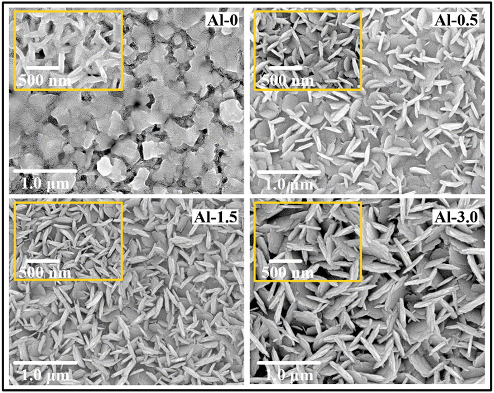 | ||
| Fig. 1 FE-SEM surface micrographs for (Cu+/Cu2+)(1−x)Al(x)S (where x = 0, 0.02, 0.06, 0.12) coded as samples Al-0 to Al-3.0. | ||
This type of surface morphology variation describes that the Al-incorporation affects both the interlayered structures and surface defect states, which varies the shape, size and thickness of the nanostructures. The general hypothesis reasons that Al3+ initially makes complexes with Cu2+, which afterward interact with S2− at the time of the crystallite nucleus aggregation processes.23 The proportion of Al-ions affects the electronegativity of the nucleation process, where at higher vacancies, it can spontaneously increase the surface energy and instability of the nanostructure.18,23 Therefore, it can be concluded that the steady state nanostructure of higher periodicity and mixed-phase assembly can only be grown with trivial doping's of Al for tuneable LSPR properties in CuS nanostructures. Moreover, the concentration of doping does not much effect the average thickness of the nanostructure and it will remain almost constant even for samples with the maximum dopant content (i.e. Al-3.0 ∼590 nm), as given in Fig. S1 of the ESI† (SI-2).
Crystalline structure
In the XRD study of the Al-doped CuS nanostructured films, the planes from the high intensity diffraction peaks of the baseline resolved spectrum matched with the covellite phase of CuS in agreement with ICDD: 03-065-3931 (lattice parameters: a = b = 3.792, c = 16.11 Å), shown in Fig. 2(a). In contrast, the diffraction peaks without baseline correction are given in Fig. S2 and SI-2 of the ESI.† The observed preferential planes at (102), (103), (006) and (110) corresponding to ∼29.5, 32.3, 33.0 and 48.3°, respectively, belong to the P63/mmc space group of hexagonal crystal symmetry with two types of bond formation for the Cu atom.11 The intra-layer planes of these structures are linked to the trigonal unit of CuS3 and further connected to the tetrahedral units of CuS4 through an interlayer vortex. The trigonal units are mainly contributed from Cu+ ions with shorter bond length (∼2.19 Å) whereas Cu2+ ions are primarily the component of tetrahedral units with larger bond length (∼2.33 Å).24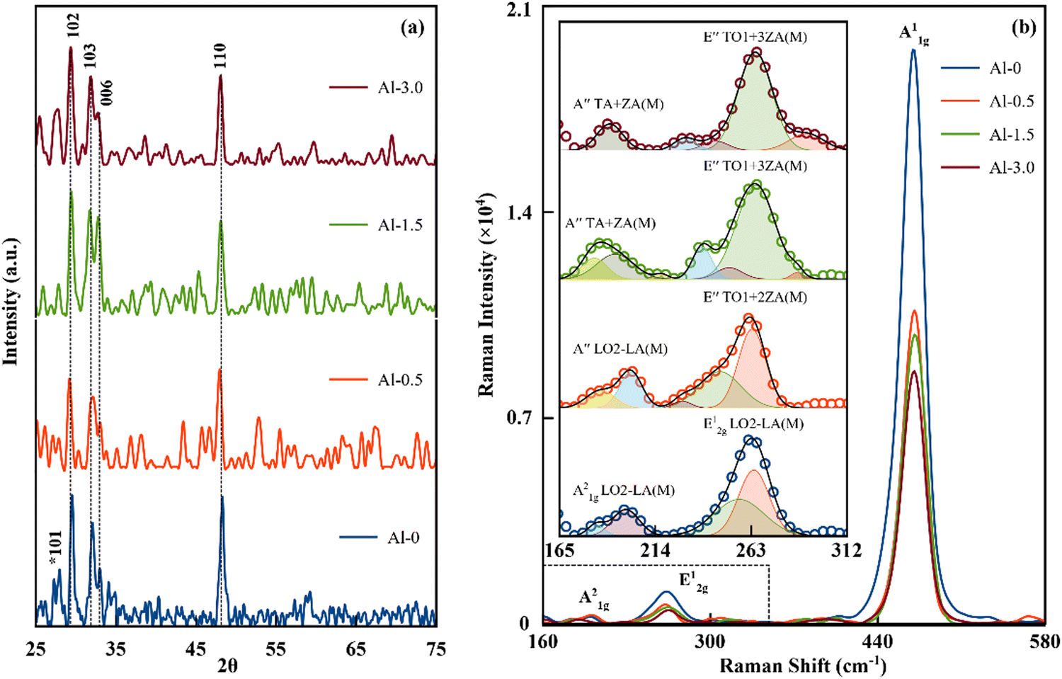 | ||
| Fig. 2 (a) The XRD patterns exhibiting the dominant hexagonal crystal structure of trigonally and tetragonally coordinated Cu–S layered networks, (b) the Raman spectra obtained under 532 nm laser excitation at room temperature, and (in the inset) deconvoluted interlayer phonon modes for A21g and E12g. Raman modes were obtained by Gaussian fitting. | ||
Experimentally, it has been observed that Al3+ can replace either ionic state of Cu but preferentially replaces Cu2+ due to its higher bond length and shorter strength. This transformation correspondingly alters the trigonally coordinated layers of Cu+ and reduces the dominant character of the (101) plane.25 As the concentration increases from Al-0.5 to Al-3.0, the intensities of the other significant planes (103) and (110) have also been trimmed. Furthermore, the standard formulation has been applied on the resolved XRD peaks to calculate various structural parameters (Table 1). Initially, the low doping content has significantly increased the dislocation density and strain in the crystallite structure of Al-0.5 that distorts the original lattice planes and reduce its particle size. As the doping concentration is increased in Al-1.5 and Al-3.0, the strain and dislocation density in the unit cells begin to decrease with a simultaneous increase in the particle size. This observed behaviour suggests that the lower concentration only participates with primary elemental bonds that develop higher instability in structure, whereas the increased doping may start participating with shallow oxide states (surface defects) and lowered the distortions within the main structure.19 These results are consistent with UV-Vis and XPS observations as discussed later.
| Sample codes | d (nm) | β (10−3 rad) | δ (10−5 m−2) | ε (×10−3) | N (cm−3) | ρ (10−3 Ω cm) | μ (cm2 V−1 s−1) | H av (10−3) |
|---|---|---|---|---|---|---|---|---|
| Al-0 | 19.7 | 7.7 | 3.89 | 1.82 | 1.77 × 10²² | 0.7 | 0.7 | 46.6 |
| Al-0.5 | 15.5 | 9.5 | 5.66 | 2.23 | 1.68 × 10¹⁹ | 32.1 | 25.6 | 80.7 |
| Al-1.5 | 16.1 | 9.2 | 5.35 | 2.16 | 1.12 × 10¹⁹ | 31.7 | 25.8 | 82.0 |
| Al-3.0 | 18.7 | 8.0 | 4.14 | 1.89 | 5.04 × 10¹⁸ | 31.5 | 61.1 | 19.2 |
Raman spectroscopy
The self-assembled multilayers of CuS nanostructures act as covalently bonded atomic layers (also known as Rigid Layers (RLs)), where adjacent layers can interact through weak van der Waals forces. Therefore, the observed distinction in Raman modes is either the result of the relative motion of RLs, vibrations between the planes of RLs or in-between shear stress and strain of the stacks.26 Here, these resonant modes from phonon–plasmon couplings have been identified as out-of-plane Cu–S (A21g), S–S bonded (A11g) and in-plane Cu–S bonded (E12g) Raman modes lying at ∼198, ∼264, and ∼474 cm−1, respectively. The apparent observation of the intensity of SERS in the A11g Raman mode signifies its reduction with respect to the decrease in carrier concentration, given in Fig. 2(b) and Table 1. The increased doping increases the shear stress and strain in-between the layers to stretch and degenerate the longitudinal and transverse optical phonon modes to ultimately reduce their resonant excitations. Furthermore, the layer dependent interactions do interesting splitting in the Cu-S bonded (in-plane) E1g and (out-of-plane) A21g mode, as shown in the inset of Fig. 2(b). These modes of D6h crystal symmetry can have degeneracy of 6 optical branches to be distributed as two in-plane longitudinal optical (LO1, LO2), two in-plane transverse optical (TO1-TO2) and two out-of-plane (ZO1 and ZO2) modes.21,27Here, the base sample has been identified with ideal layer dependent degeneracy, where the soft phonon mode lying at ∼198 cm−1 has split into A21g(M) LO2-LA(M) branches signifying the second order scattering process from two phonons.27,28 The high frequency E12g mode is interlayered symmetry sensitive to have branches as E12g(M) LO2 + LA(M), exhibiting an enhancement in the electron–phonon coupling.26,29 As the doping commenced, the interlayer strain and stress renders new split off branches in the E12g mode to further create hybrid modes in A21g though mutual interactions. With the increase in doping content, the degeneracy in the E12g mode can be registered in the second and third phonon branches of the transverse and out-of-plane dispersion modes as E′′(M)TO1 + 2ZA(M) and E′′(M)TO1 + 3ZA(M) while A21g can split as phonon replicas in the combination of LA(M) + TA(M) and LA(M) + ZA(M) modes towards the higher or lower side of binding energy.21,26–29 Here, the resulting degeneracy linearly increases with the dopant concentration, as shown in the inset of Fig. 2(b). Therefore, it can be concluded that the dopant dependent interlayer tensions can broaden the phonon–plasmon resonant excitations of this system.
Hall measurements
The information on the charge carrier concentration, mobility, resistivity and average Hall coefficient has been measured from Hall measurements, given in Table 1. The pure sample Al-0 exhibits intrinsic mobility of multi-layer hexagonal structures, which is expected to be low according to acoustic deformation potential theory (DPT).30 It approximates that the layered structures have significant peak-valley scatterings in the electronic structure due to long wavelength longitudinal acoustic (LA) phonons. The increasing incorporation of Al3+ leads to a linear decrease in the carrier concentration and simultaneously creates obvious complementing behaviour for mobility. The apparent explanation states that the smaller radii of Al-ions act as shallow defect states for the sites of both Cu2+ and surface oxide states.30,31 Therefore, their concentration dependent substitution offers a different type of thermodynamic electron/hole trap sites, which have been well complemented in the XPS results. However, it has to be noticed that the progressed density of states (DOS) has significantly improved the relative mobility in doped samples. The preceding explanation based on DPT states that the increased DOS may align the peak–peak and peak–valley bands at the sharp Γ point (Brillouin zone) in the electronic structure to induce better spin–orbit coupling effects.30Reflectance spectroscopy
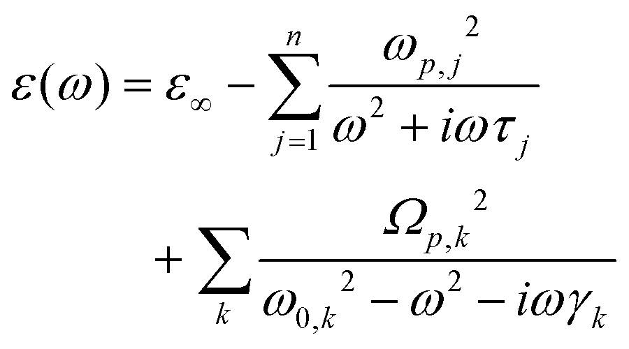
The experimental data of diffuse reflectance spectra in near normal incidence mode have been fitted to the semi-classical Drude–Lorentz model to describe mutual interactions between intraband (free electrons/plasmons) and interband (bound electrons/excitons) transitions.32,33 A qualitative analysis has been performed using the RefFIT program in consideration of various experimental parameters that effect screen plasmon edge and intensity of reflectivity in the case of thin films on a glass substrate.34 The following complex dielectric function is used in non-linear least squares fit to gain insights into their refractive index and dispersive behaviour, where detail on the parameters is given in the ESI† (SI-3 and SI-5).The estimated values from these fittings for both oscillators have been given in Tables S1–S4 of the ESI† (SI-4). In accordance with our last fitting analysis,11,21 we procure precise values of physical parameters such as ε∞, ωo, ωp and ϒ (for Drude oscillator, given in Table 2) to extract genuine behaviour of complex optical dispersions in terms of refractive index and dielectric constants for CuS:Al nanostructured films.
| Samples | E g (eV) | ε ∞ | ω p (cm−1) | ϒ (cm−1) | ω sp (cm−1) | Q sp | z (nm) |
|---|---|---|---|---|---|---|---|
| Al-0 | 2.42 | 1.85 | 19028 |
1749 | 11134 |
0.62 | 461 |
| Al-0.5 | 2.66 | 1.95 | 18870 |
4104 | 10191 |
0.54 | 209 |
| Al-1.5 | 2.63 | 1.95 | 15197 |
4039 | 7872 | 0.49 | 370 |
| Al-3.0 | 2.60 | 2.06 | 22405 |
8953 | 9159 | 0.43 | 352 |
The edge shift and intensity variations of the reflectance spectra have been traced to discover the red energy shift between surface plasmons and electronic transitions for mildly doped samples (Al-0.5 and Al-1.5), whereas a blue shift is observed for the heavily doped nanostructure (Al-3.0), with the values given in Table 2. The initial two substitutions abbreviate the phase velocities (momentum) of plasmon excitations in CuS nanostructures due to structural distortions, which increases their relaxation coefficient to red shift the coupled excitations.21,33,35 The further increase of dopant concentration might have commenced the UV-Vis region plasmonic excitations of Al that have blue shifted the overall plasmon edge with increased relaxation coefficient (FWHM). Simultaneously, the refractive index obeying these dynamics got tuned towards larger values for which epsilon-near-zero (ENZ) modes in permittivity have been shifted towards longer wavelengths, covering a wide spectral region, as shown in Fig. 3(c) and (d). These observations also conclude that the coupled excitation from increased structural deformations tends to have more Fano-resonances that simultaneously increase the anomalous behaviour of optical and dielectric constants.36,37 The corresponding trends for the imaginary parts of both coefficients are also given in Fig. 3(c) and (d). Therefore, it can be concluded that the doping of Al can provide variable resonant excitations for tuneable ENZ modes in a different range of frequencies.
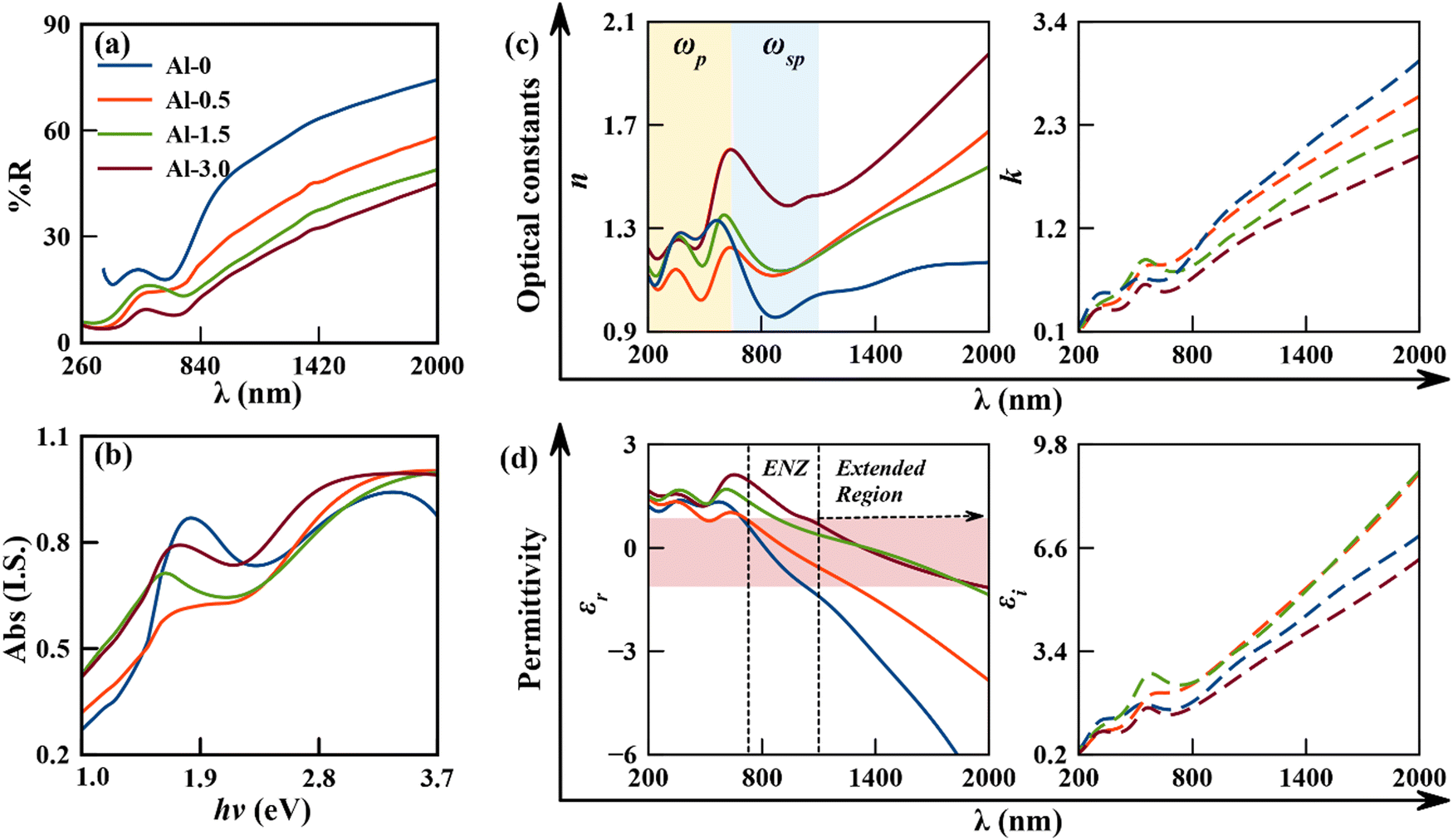 | ||
| Fig. 3 (a) Diffuse reflectance spectra (measured in near normal incidence mode) as fitted to the Drude–Lorentz oscillator model; (b) transposed normalized absorption spectra; (c) the extracted values of refractive index (n) and extinction coefficient (k); and (d) the real part of the permittivity (εr) depicting improved dispersion modes and imaginary permittivity (εi) with substitution of Al3+ ions in the CuS nanostructures. | ||
UV-Vis-NIR absorption spectroscopy
The measured linear absorption spectrum and the corresponding estimated band gaps using the Tauc plot have been given in (a and b) of Fig. 4, and are observed to be at ∼2.42, ∼2.66, ∼2.63 and ∼2.60 eV for Al-0, Al-0.5, Al-1.5, and Al-3.0, respectively. The spectral line widths of the coupled inter-excitonic and plasmonic interactions are masked by inhomogeneous broadenings into peak components of absorption spectra. The relative variation in periodic energy exchange of exciton–plasmon excitations has been resolved by the Gaussian peak fitting approach,10,11 given in Fig. S3 of the ESI† (SI-6). This analogy is used frequently in support of the employed Drude–Lorentz model on the diffuse reflectance spectrum.11,37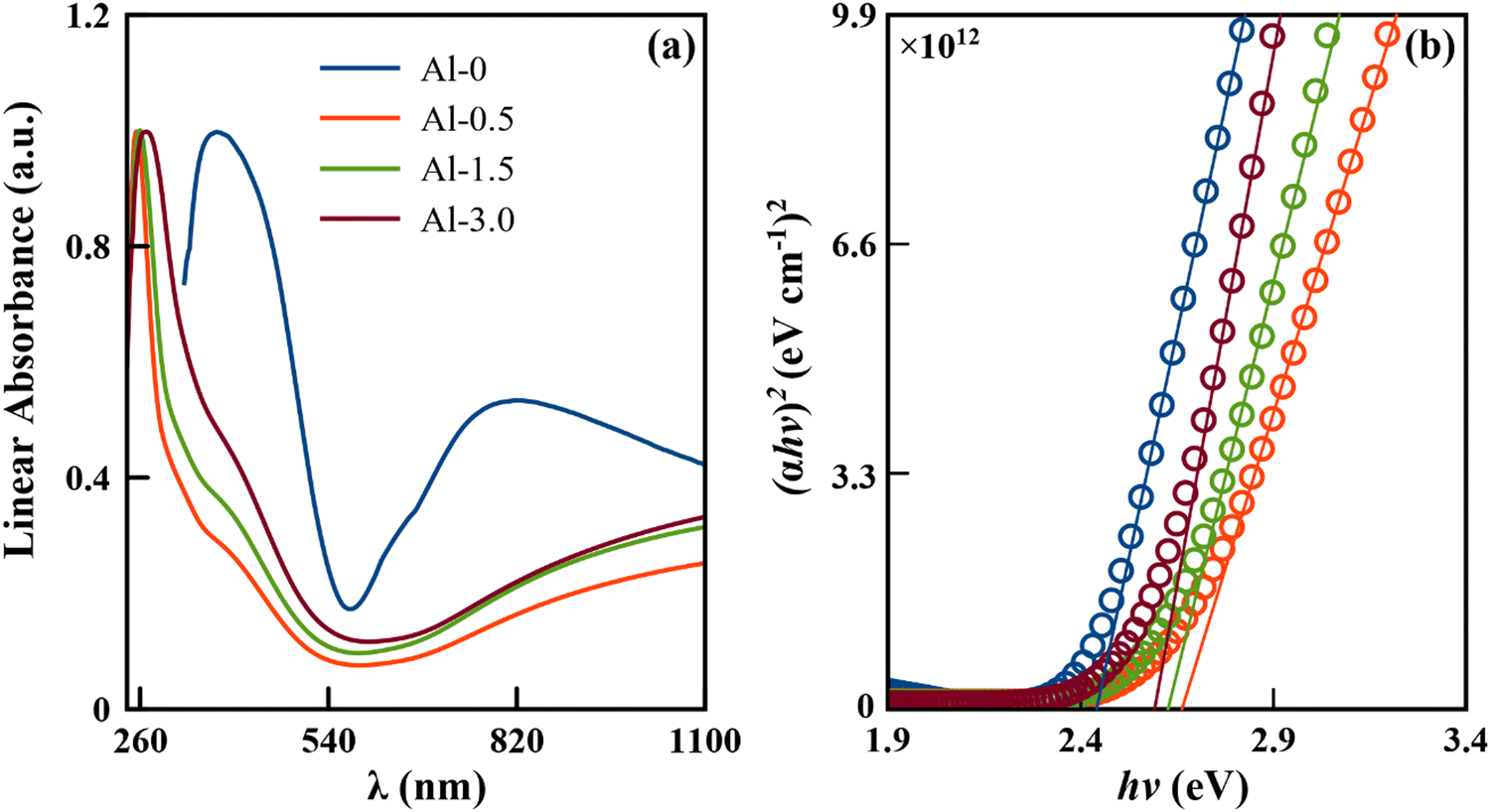 | ||
| Fig. 4 (a) UV-Vis-NIR absorbance spectrum; (b) Tauc plot for highly coupled assemblies of intrinsic and doped CuS nanostructures. | ||
Now according to the observed behaviour, the doping plays a significant role in annihilating the renormalized band gap phenomena of our base sample, as discussed in our previous analysis.11,21 The pure sample (Al-0) has a reduced band gap due to electron–electron or electron–ion interactions of many-body particle systems. It has been swapped with the quantum confinement effect for the low-doped sample (Al-0.5), which is supplemented from the decreased carrier concentration and significant particle size reduction for the consequently increased bandgap. As the doping concentration increases in Al-1.5 and Al-3.0, the carrier concentration simultaneously keeps on decreasing, but the particle size follows an increasing trend that further reduces the bandgap edge, following both Brustein–Moss and quantum confinement effects. In addition to the former discussion, the low doping in these p-type semiconducting nanostructures can create vacancies in the valence band to drag the acceptor levels deeper and results in the broadening of the band gap.38,39 In contrast, relatively significant doping can neutralize the vacancies for oxidized surface defect states to result in a reduction of the carrier concentration with slight narrowing of the bandgap.38,39
XPS spectroscopy
The influence of Al doping on the oxidation and electronic states of CuS has been analysed from XPS spectroscopy. The survey scan shows the elemental peaks for Al, Cu, S, O and C, and their relative at% are given in Fig. S4 (ESI,† SI-7). The deconvolution of the magnified peaks in different ranges of binding energy (B.E.) demonstrated the effects of Al on existing states of Cu and S, given in Fig. 5. The signature peaks for Cu, i.e. 2p3/2 and 2p1/2 at ∼932.28 eV and ∼952.18 eV, respectively, are precisely registered to the Cu+ oxidation state.18,40 The contribution of Cu0 from probabilistic formation of complexes and oxide phases due to the presence of dual Cu+/Cu2+ salts is found to be developed at ∼932.70 eV (2p3/2) and ∼952.90 eV (2p1/2) to be consistent with our previous work.11 Similarly, the deconvoluted phase for Cu2+ does adequately fit at ∼934.40 eV (2p3/2) and ∼956.20 eV (2p1/2) and their variation subsequently distinguishes the modifications in unsaturated (d9) electronic configuration and p–d hybridizations.41 Here, the incremental addition of Al from Al-0.5 to Al-3.0 linearly abbreviates the intensity of the Cu complexes and Cu2+ peaks significantly. These results are in accordance with the XRD observations to further conclude that the Al-doping primarily substitutes at the Cu2+ site and surface defect states. Similar de-convolutions for sulfur valence states have been identified in the form of a doublet at 161.28 eV (2p3/2) and 163.28 eV (2p1/2) for sulfides and at 162.18 eV (2p3/2) and 164.38 eV (2p1/2) for disulfides, while the characteristic peak for sulfur complexes is distinguished at ∼169.08 eV.42 However, the addition of Al doesn’t directly influence the normalized intensities of the sulfide peaks, but it interacts with their complexes and completely depletes them at its maximal dopant concentration, again signifying the formation of surface defect states through Al oxidation.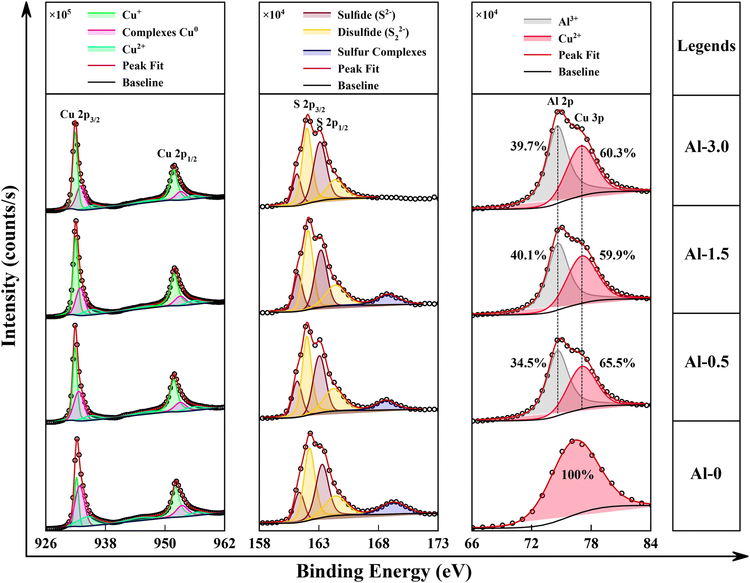 | ||
| Fig. 5 The high-resolution Cu (2p), S (2p) and Cu (3p) XPS spectra for highly coupled CuS nanostructures in intrinsic and Al-doped assemblies. The deconvoluted linewidth of subcomponents using the best mixture of Gaussian–Lorentzian components is displayed in different colours. The relative at% of Al–O to Cu2+ vacancies in Al 2p and Cu 3p states, respectively, is also given. | ||
Finally, the observation that directly demonstrates the presence of Al in CuS is derived in the deconvoluted spectra of Cu 3p, also given in Fig. 5. The characteristic peak at 77.8 eV corresponds to the Cu 3p orbital for the Cu2+ oxidation state, whereas the peak at 74.3 eV is standardized to Al–O bond in Al3+ oxidation state. Now, the peak areas from Fig. 5 have been used to estimate the variation in Al–O states exclusively to Cu2+ states.43,44 Simultaneously, the total relative change in Al-content with respect to all other present species has been evaluated from the area of all significant peaks in the XPS survey scan43,44 and is given in Fig. S4 and its inset, SI-7 of the ESI.† Here, the relative concentration of Al with respect to all other present elements in the synthesized nanostructures is approximated as 4.5%, 5.9% and 5.7% for Al-0.5, Al-1.5 and Al-3.0, respectively. It has been observed that the role of aluminium doping is complicated as it interacts with both the copper oxidation and oxide defect states as exhibited in Fig. S5 and SI-7 of the ESI.† Therefore, an increase in Al3+ content correspondingly increases the Al-O states around ∼74.3 eV until Al-1.5 but has been reduced for the sample with maximal Al content (Al-3.0). This effect of doping on oxide reducibility suggests that the decreased Al–O concentration has been utilized to reduce the sulfur complexes as observed simultaneously.45
Valence band spectra
The variation of the LSPR and optical band gap edge can be better understood by analysing the variation of electronic states in the valence band (VB) XPS spectra as given in Fig. 6. The density of states (DoS) has been resolved for the maximum intensity band and entailed the valence band using Gaussian peak distribution, as given in Fig. 6(a) and (b), which is similar to earlier reports.11,21,46 The determined onset edge of both the valence bands (EVB) has been used in the formula EVBM = Ef − EVB (where, Fermi energy (Ef) = 0) to calculate valence band maxima.41,47 Furthermore, these values along with the respective values of optical band gap are used to calculate the probable lower edge of the conduction band, as ECB = 0.82, 1.24, 1.12 and 1.11 eV for sample Al-0, Al-0.5, Al-1.5 and Al-3.0, respectively. It has been observed that the trivial doping of Al3+ in sample Al-0.5, abruptly intensifies the density of defect states and lattice strains to create shallow defect states over the valence band. Then, the interactions of Al3+ and Cu2+ ions at the lower end of the conduction band have significant electron–hole pair extraction within shallow defect states of the valence band.39,41 This mechanism reduces carrier concentration, which leaves more hole sites to push the conduction band away as well as the Fermi level deeper into the valence band states and may have improved the p-type conductive response. As the concentration of doping further increases, the interaction between Al3+ and Cu2+ ions within the excitonic trap sites of the conduction band also increases to further keep on reducing the carrier concentration. Simultaneously, they extract the oxygen vacancies to deplete the oxide defect states over the valence band to again pull both the CB and VB back towards the original B.E. levels.18,19,39 This remarkable behaviour also complements the ascertained variations of all elemental oxidation states and the optical band gap for this system. The Al3+ concentration-dependent complex interaction mechanism varies the stoichiometric, physical and electronic structures of Cu+/2+ and S−/2− states for enhanced plasmon driven optical responses of the synthesized CuS nanostructured films.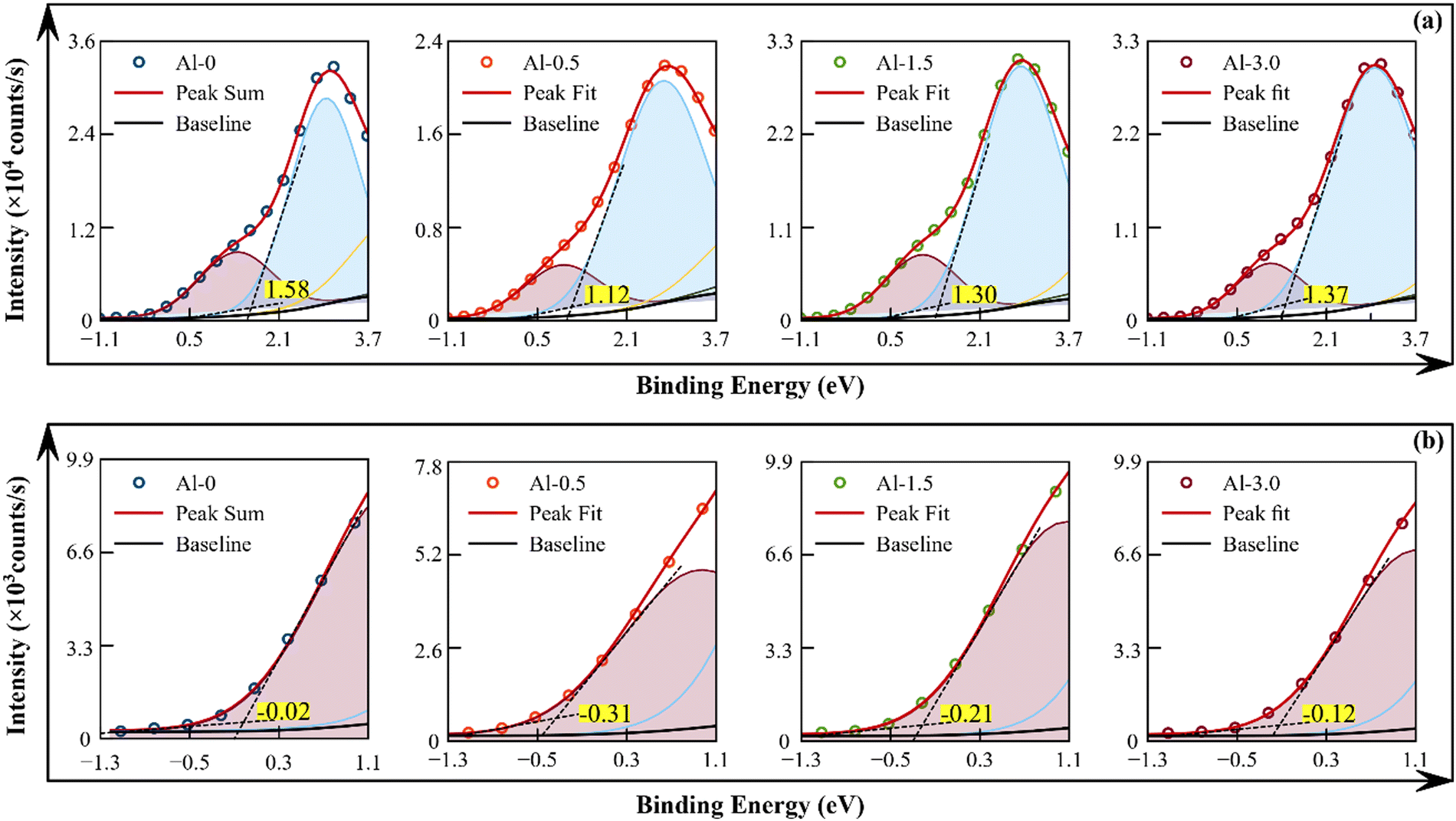 | ||
| Fig. 6 (a) The deconvoluted density of states (DoS) for the maximum and entailed valence band with different colour coding. Both edges have been used to calculate the valence band maximum (VBM) and the conduction band minimum (CBM) using the standard formulation; (b) an expanded view of the entailed VBM near the Fermi energy centred at 0 eV. | ||
Conclusion
In summary, we have successfully synthesized Al-doped CuS heterostructures for critical excitonic and plasmonic transition properties. The increased concentration of the dopant depletes the dynamics of many-body particle interactions, whereas it increases the coulomb and van der Waals interactions, following Burstein–Moss and quantum confinement effects. The modified spatial characteristics of the Al-doped nanostructures are due to changes in charge carrier concentration and relative mobility, abided by the reduced peak-valley scatterings and improved spin–orbit couplings. The enhanced interlayered electron–phonon interactions have been traced in splitting of the optical phonon branches of the (in-plane) E12g and (out-of-plane) A12g Raman modes. The doping driven abbreviated phase velocities and relaxation coefficients tunned the dielectric coefficients for enhanced ENZ optical modes, which were effectively studied with the Drude–Lorentz model fitting in the near normal incident mode reflectance spectrum. The resolved linear absorption spectra using Gaussian line-shape fittings signify the respective variations in excitonic and plasmonic states that support the transposed absorption dynamics from the diffuse reflectance spectrum. The shift in the electronic states and valence band gives reasonable values to understand the orbital hybridization in the deeper valence and higher conduction band regions of the coupled system. Our findings prove that the Al-doping in the CuS nanostructures can produce stacked 2D vertical heterostructures that can have effective tuning in carrier mobility and dispersion modes for applications in highly efficient future optoelectronic devices.Conflicts of interest
There are no conflicts to declare.Acknowledgements
The authors gratefully acknowledge the SAIF, Panjab University, Chandigarh for XRD and FE-SEM measurements; MNIT, Jaipur for Raman spectroscopy and Hall measurements; AMRC, IIT Mandi for XPS measurements and SAIF, CSIR-CECRI, Karaikudi for Reflectance spectroscopy.References
- Y. Lin, X. Ling, L. Yu, S. Huang, A. L. Hsu, Y. H. Lee, J. Kong, M. S. Dresselhaus and T. Palacios, Nano Lett., 2014, 14, 5569 CrossRef CAS PubMed.
- X. Zhu, J. He, R. Zhang, C. Cong, Y. Zheng, H. Zhang, S. Zhang and L. Chen, Nanoscale, 2020, 12, 23732 RSC.
- S. Dufferwiel, S. Schwarz, F. Withers, A. A. P. Trichet, F. Li, M. Sich, O. Del Pozo-Zamudio, C. Clark, A. Nalitov, D. D. Solnyshkov, G. Malpuech, K. S. Novoselov, J. M. Smith, M. S. Skolnick, D. N. Krizhanovskii and A. I. Tartakovskii, Nat. Commun., 2015, 6, 8579 CrossRef CAS PubMed.
- W. Liu, B. Lee, C. H. Naylor, H.-S. Ee, J. Park, A. T. C. Johnson and R. Agarwal, Nano Lett., 2016, 16, 1262 CrossRef CAS PubMed.
- W. Liu, Y. Wang, C. H. Naylor, B. Lee, B. Zheng, G. Liu, A. T. C. Johnson, A. Pan and R. Agarwal, ACS Photonics, 2018, 5, 192 CrossRef CAS.
- V. Giannini, A. I. Fernández-Domínguez, Y. Sonnefraud, T. Roschuk, R. Fernández-García and S. A. Maier, Small, 2010, 6, 2498 CrossRef CAS PubMed.
- S.-W. Hsu, C. Ngo and A. R. Tao, Nano Lett., 2014, 14, 2372 CrossRef CAS PubMed.
- M. Lee, J. Yang, H. K. Lee, J. I. Lee, A. R. Koirala, J. Park, H. Jo, S. Kim, H. Park, J. Kwak, H. Yoo, W. Huh and M. S. Kang, ACS Appl. Mater. Interfaces, 2021, 13, 26330 CrossRef CAS PubMed.
- L. Shi, T. K. Hakala, H. T. Rekola, J.-P. Martikainen, R. J. Moerland and P. Törmä, Phys. Rev. Lett., 2014, 112, 153002 CrossRef CAS PubMed.
- E. S. H. Kang, S. Chen, S. Sardar, D. Tordera, N. Armakavicius, V. Darakchieva, T. Shegai and M. P. Jonsson, ACS Photonics, 2018, 5, 4046 CrossRef CAS.
- H. Singh, S. Kumar and P. K. Sharma, Appl. Surf. Sci., 2023, 612, 155831 CrossRef CAS.
- V. Kochergin, L. Neely, C. Y. Jao and H. D. Robinson, Appl. Phys. Lett., 2011, 98, 133305 CrossRef.
- Q. Gao, X. Wu and T. Huang, Sol. Energy, 2021, 220, 1–7 CrossRef CAS.
- C. Hu, W. Chen, Y. Xie, S. K. Verma, P. Destro, G. Zhan, X. Chen, X. Zhao, P. J. Schuck, I. Kriegel and L. Manna, Nanoscale, 2018, 10, 2781 RSC.
- G. Liu, S. Qi, J. Chen, Y. Lou, Y. Zhao and C. Burda, Nano Lett., 2021, 21, 2610 CrossRef CAS PubMed.
- M. Liu, Y. Liu, B. Gu, X. Wei, G. Xu, X. Wang, M. T. Swihart and K. T. Yong, Chem. Soc. Rev., 2019, 48, 4950 RSC.
- Y. Xie, W. Chen, G. Bertoni, I. Kriegel, M. Xiong, N. Li, M. Prato, A. Riedinger, A. Sathya and L. Manna, Chem. Mater., 2017, 29, 1716 CrossRef CAS PubMed.
- X. Dai, H. Lei, C. Chen, Y. Guo and G. Fang, RSC Adv., 2018, 8, 16887 RSC.
- J. Jing, X. Gu, S. Zhang, J. Sun, Y. Chen and T. Sun, CrystEngComm, 2019, 21, 4969 RSC.
- D. Gerard and S. K. Gray, J. Phys. D: Appl. Phys., 2015, 48, 184001 CrossRef.
- H. Singh, I. Arora, V. Natarajan, S. Kumar and P. K. Sharma, J. Phys. Chem. C, 2023, 127, 11623–11631 CrossRef CAS.
- S. A. McLuckey and T. Y. Huang, Anal. Chem., 2009, 81, 8669 CrossRef CAS PubMed.
- C. Guo, C. Yang, Y. Xie, P. Chen, M. Qin, R. Huang and F. Huang, RSC Adv., 2016, 6, 40806 RSC.
- A. Morales-García, A. L. Soares, E. C. Dos Santos, H. A. De Abreu and H. A. Duarte, J. Phys. Chem. A, 2014, 118, 5823 CrossRef PubMed.
- L. Duclaux, F. Donsanti, J. Vidal, M. Bouttemy, N. Schneider and N. Naghavi, Thin Solid Films, 2015, 594, 232 CrossRef CAS.
- X. Zhang, X. F. Qiao, W. Shi, J. Bin Wu, D. S. Jiang and P. H. Tan, Chem. Soc. Rev., 2015, 44, 2757 RSC.
- X. Zhang, Q. H. Tan, J. Bin Wu, W. Shi and P. H. Tan, Nanoscale, 2016, 8, 6435 RSC.
- S. Cortijo-Campos, P. Kung, C. Prieto and A. de Andrés, J. Phys. Chem. C, 2021, 125, 23904 CrossRef CAS.
- J. Pandey, S. Mukherjee, D. Rawat, S. Athar, K. S. Rana, R. C. Mallik and A. Soni, ACS Appl. Energy Mater., 2020, 3, 2175 CrossRef CAS.
- L. Cheng, C. Zhang and Y. Liu, J. Am. Chem. Soc., 2019, 141, 16296 CrossRef CAS PubMed.
- F. A. Sabah, N. M. Ahmed, Z. Hassan and H. S. Rasheed, Procedia Chem., 2016, 19, 15 CrossRef CAS.
- T. Gharbi, D. Barchiesi, S. Kessentini and R. Maalej, Opt. Mater. Express, 2020, 10, 1129 CrossRef.
- K. Zhang, Y. Du, Z. Qi, B. Cheng, X. Fan, L. Wei, L. Li, D. Wang, G. Yu, S. Hu, C. Sun, Z. Huang, J. Chu, X. Wan and C. Zeng, Phys. Rev. Appl., 2020, 13, 014058 CrossRef CAS.
- A. B. Kuzmenko, Rev. Sci. Instrum., 2005, 76, 083108 CrossRef.
- K. Sun, R. Fan, Y. Yin, J. Guo, X. Li, Y. Lei, L. An, C. Cheng and Z. Guo, J. Phys. Chem. C, 2017, 121, 7564 CrossRef CAS.
- Y. B. Zheng, B. Kiraly, S. Cheunkar, T. J. Huang and P. S. Weiss, Nano Lett., 2011, 11, 2061 CrossRef CAS PubMed.
- T. Tumkur, Y. Barnakov, S. T. Kee, M. A. Noginov and V. Liberman, J. Appl. Phys., 2015, 117, 103104 CrossRef.
- T. Edvinsson, R. Soc. Open Sci., 2018, 5, 180387 CrossRef CAS PubMed.
- B. A. D. Williamson, J. Buckeridge, J. Brown, S. Ansbro, R. G. Palgrave and D. O. Scanlon, Chem. Mater., 2017, 29, 2402 CrossRef CAS.
- M. C. Biesinger, Surf. Interface Anal., 2017, 49, 1325 CrossRef CAS.
- J. Ludwig, L. An, B. Pattengale, Q. Kong, X. Zhang, P. Xi and J. Huang, J. Phys. Chem. Lett., 2015, 6, 2671 CrossRef CAS PubMed.
- M. Fantauzzi, B. Elsener, D. Atzei, A. Rigoldi and A. Rossi, RSC Adv., 2015, 5, 75953 RSC.
- Y. Wang, Y. Lü, W. Zhan, Z. Xie, Q. Kuang and L. Zheng, J. Mater. Chem. A, 2015, 3, 12796 RSC.
- A. Liu, G. Liu, H. Zhu, B. Shin, E. Fortunato, R. Martins and F. Shan, RSC Adv., 2015, 5, 86606 RSC.
- A. R. Puigdollers, P. Schlexer, S. Tosoni and G. Pacchioni, ACS Catal., 2017, 7, 6493 CrossRef.
- T. J. Whittles, T. D. Veal, C. N. Savory, A. W. Welch, F. W. De Souza Lucas, J. T. Gibbon, M. Birkett, R. J. Potter, D. O. Scanlon, A. Zakutayev and V. R. Dhanak, ACS Appl. Mater. Interfaces, 2017, 9, 41916 CrossRef CAS PubMed.
- L. Liu, B. Zhou, L. Deng, W. Fu, J. Zhang, M. Wu, W. Zhang, B. Zou and H. Zhong, J. Phys. Chem. C, 2014, 118, 26964 CrossRef CAS.
Footnote |
| † Electronic supplementary information (ESI) available. See DOI: https://doi.org/10.1039/d3ma00418j |
| This journal is © The Royal Society of Chemistry 2023 |