
 Open Access Article
 This Open Access Article is licensed under a
 Creative Commons Attribution 3.0 Unported Licence
Exposure to solvent vapours for enhanced N-type OTFT stability†
Samantha
Brixi
a,
Halynne R.
Lamontagne
 ab,
Benjamin
King
a,
Adam J.
Shuhendler
bcd and
Benoît H.
Lessard
*ae
ab,
Benjamin
King
a,
Adam J.
Shuhendler
bcd and
Benoît H.
Lessard
*ae
aUniversity of Ottawa, Department of Chemical and Biological Engineering, 161 Louis Pasteur, Ottawa, ON, Canada. E-mail: benoit.lessard@uottawa.ca
bUniversity of Ottawa, Department of Chemistry and Biomolecular Sciences, 150 Louis Pasteur, Ottawa, ON, Canada
cUniversity of Ottawa, Department of Biology, 30 Marie Curie, Ottawa, ON, Canada
dUniversity of Ottawa Heart Institute, 40 Ruskin St, Ottawa, ON, Canada
eUniversity of Ottawa, School of Electrical Engineering and Computer Science, 800 King Edward Ave, Ottawa, ON, Canada
First published on 26th July 2023
Abstract
To achieve commercialization of organic electronics, the field must see an improvement in both performance and material stability while maintaining a low cost of fabrication. To achieve this, low-cost additives provide a viable solution. A variety of additives containing amine and silane functional groups were tested to determine their impact on the performance and air-stability of n-type semiconductor poly{[N,N′-bis(2-octyldodecyl)-naphthalene-1,4,5,8-bis(dicarboximide)-2,6-diyl]-alt-5,5′-(2,2′-bithiophene)} (P(NDI2OD-T2)) in organic thin film transistors. Aniline and pyridine were found to both have a minimal impact on P(NDI2OD-T2) performance in an inert environment, but to improve stability of electron mobility and threshold voltage in air. Therefore, these compounds, or other compounds based on their structure, would be ideal candidates as additives for the improvement of n-type transistors.
Introduction
The stability of organic semiconducting materials used in n-type electronic devices must see improvement before widespread commercial adoption. While new complex materials are being developed and incremental improvements in performance are made, improving device performance using already commercially viable semiconductors is another promising strategy.1,2 For example, the use of additives in ink formulations, thin film treatment or the use of encapsulation can improve the overall performance and stability without the need of synthesizing a new semiconductor. These techniques can be used in tandem to enable enhanced stability.Numerous additives have been shown to improve organic thin-film transistors (OTFTs) by altering film morphology or acting as dopants.3–8 It has previously been reported that the presence of various solvent molecules within a film can enhance performance and stability of p-type materials.8 Films of n-type semiconductors exposed to vapours of aminosilane molecules displayed enhanced performance,9 but their stability was not studied. Aminosilanes contain two separate functional groups: an electron-donating amine and an electron-withdrawing silane. Amine molecules have been used as n-type dopants,7,10 while silanes have been used as p-type dopants.11 The two functionalities could potentially have disparate effects. The silane group would be likely to have high reactivity with water and may enhance stability of the device by preferentially reacting with water and preventing interaction with the semiconductor. Isolating the effect of each functional group and developing structure property relationships between additives and the resulting n-type stability will lead to the design of high performance and stable n-type devices.
In this study we explore the use of commercially available solvents such as aminosilanes, amines, and silane molecules having similar size and structure. Bottom gate top contact (BGTC) OTFTs were fabricated using commercially available P(NDI2OD-T2) (poly{[N,N′-bis(2-octyldodecyl)-naphthalene-1,4,5,8-bis(dicarboximide)-2,6-diyl]-alt-5,5′-(2,2′-bithiophene)}), then treated with various aminosilanes, amines, and silanes to determine the impact of these compounds on device performance (Fig. 1).
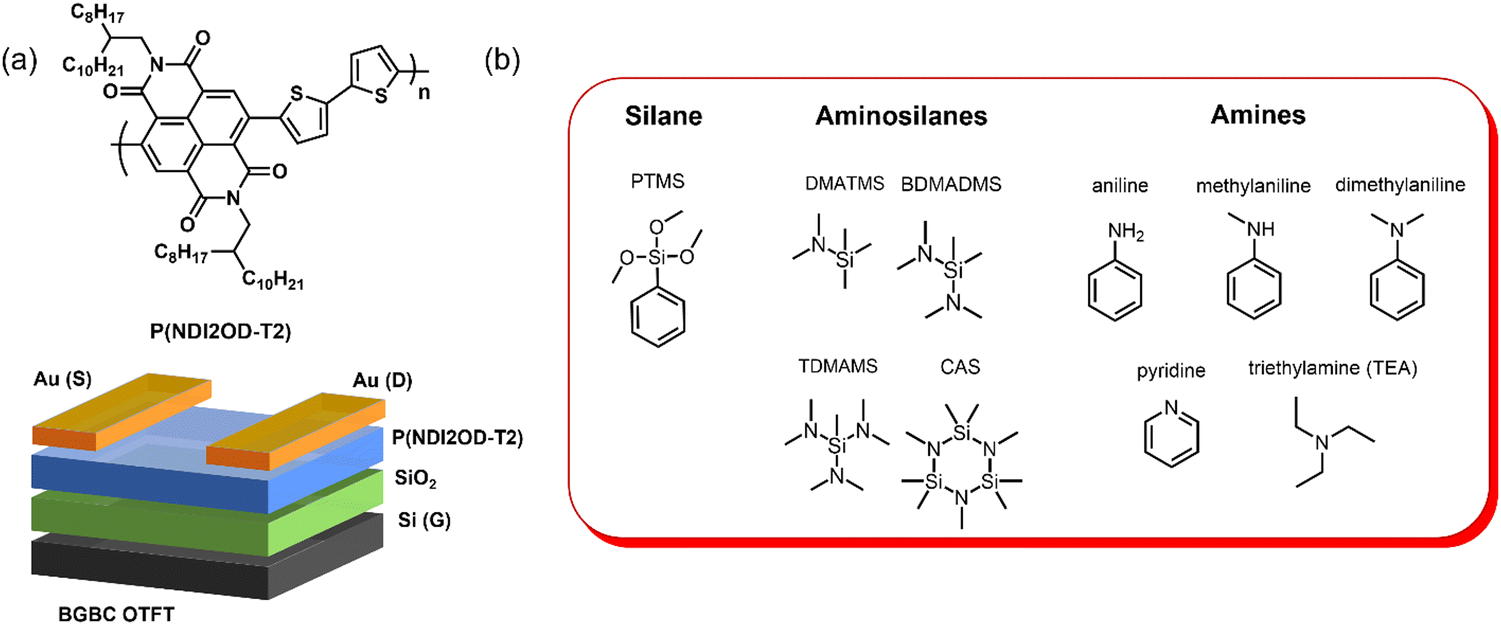 | ||
| Fig. 1 (a) Structure of P(NDI2OD-T2) and OTFT configuration. (b) Aminosilane, amine, and silane additives used in this study. | ||
Discussion
Typical BGTC P(NDI2OD-T2) OTFTs were fabricated according to literature.12 After fabrication, devices were characterized under inert conditions in a N2 glovebox. The control sample, which was not exposed to any vapour, was then exposed to air and characterized again (Fig. 2). The remaining devices were all exposed to the respective solvent vapour for 30 minutes, then characterized in the same glovebox environment immediately after vapour exposure was completed to compare performance before and after exposure (devices remained in the glovebox for the duration of the experiment). Directly following testing under inert conditions, these vapour-exposed devices were then moved to air and characterized again, which would allow the impact on air stability to be assessed. Immediate testing after air exposure ensured that the effects of each additive could be assessed directly without concern from any difference in relative volatility or preferential film adsorption, which will allow for the identification of ideal functional groups in the future design of additives.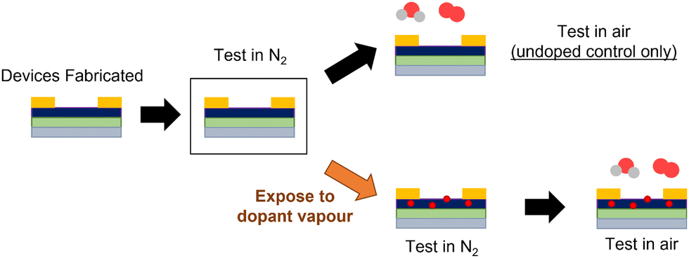 | ||
| Fig. 2 Visual schematic of methodology of characterizing P(NDI2OD-T2) OTFT air stability with solvent vapour exposure. | ||
Fig. 3 shows the saturation electron mobility (μe) and threshold voltage (VT) of OTFTs fabricated with P(NDI2OD-T2) and treated with various solvent additives. For each of the following comparisons, the comparison is made with the initial performance of the same device before exposure to the additive and exposure to air. These are then compared to the untreated devices (left-hand side of the figure) for comparison of the impact of air exposure. Typically, a modest increase in VT and a drop in μe is observed for P(NDI2OD-T2) based OTFTs13 when operated in air, which was observed for the untreated samples. The (dimethylamino)trimethylsilane (DMATMS) and bis(dimethylamino)trimethylsilane (BDMADMS) both increased the μe of the devices after initial exposure. However, the tris(dimethylamino)trimethylsilane (TDMAMS) and cyclic aminosilane (CAS) both led to decreased μe after initial exposure. All of the trimethylsilanes retained μe values in air that were higher than the control, however DMATMS exhibited the smallest overall change in μe from inert atmosphere to air. Increasing the relative nitrogen content of the silane worsened its ability to retain the μe in air. All vapour treatments resulted in an increased VT under inert conditions compared to the untreated film of approximately 5 to 10 V. After air exposure, regardless of the vapour the devices were exposed to, the VT of all devices were in the range of 30 to 35 V. While there is some evidence that aminosilanes may improve device stability with DMATMS retaining higher mobility in air, the small impact on VT in air was less promising.
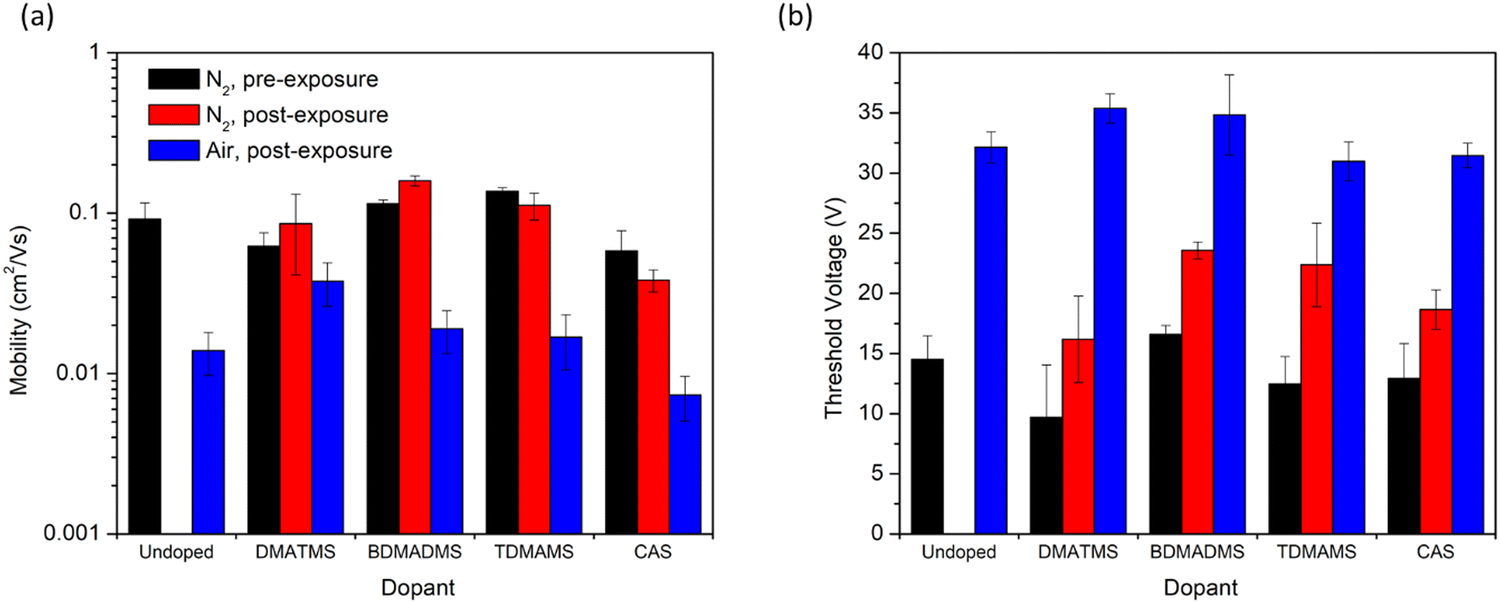 | ||
| Fig. 3 (a) Saturation electron mobility and (b) threshold voltage of devices before and after vapour exposure to aminosilane vapours under inert conditions, and subsequent changes in performance after exposure to air. | ||
As the amine group is likely to be the main source of n-doping in these devices,7 it was therefore of interest to study exposure of the devices to primary, secondary, and tertiary amines to determine if this impacted the n-doping effect (Fig. 4). Therefore, the addition of aniline, N-methylaniline, and N,N-dimethylaniline to the OTFTs were all characterized. All three had little impact on μe under inert conditions, and all three resulted in higher μe in air compared to the control. However, only the primary amine, aniline, led to a lower VT than the control. Devices that had been exposed to methyl- or dimethylaniline displayed greater VT compared to the control. Increasing VT was observed with increasing methylation of the aniline. Similarly, the tertiary amine triethylamine also resulted in a VT nearly triple that of the control (Fig. 4). This reduced performance by tertiary amines may explain why the performance of aminosilanes decreased with increasing nitrogen content, as all amines present in the molecules were tertiary amines. Pyridine displayed the greatest overall μe retention in air and also displayed a VT comparable to the control. Pyridine and aniline both have lower pKa and ionization potential than alkyl amines.14 The lower ionization potential may enable the pyridine and aniline to more readily contribute an n-type doping effect, but the trend is not consistent throughout all the additives suggesting there are likely multiple factors at play such as diffusion and molecular geometry. To confirm that the effects observed in this study were due to interactions between the additives and the semiconductor, rather than an impact on the film morphology, GIWAXS scattering patterns were obtained (Fig. S1, ESI†). No differences in peak locations or evolution of new peaks were observed in the in-plane scattering (Fig. S2, ESI†), suggesting that additive exposure did not result in changes in the packing mode of the thin film.
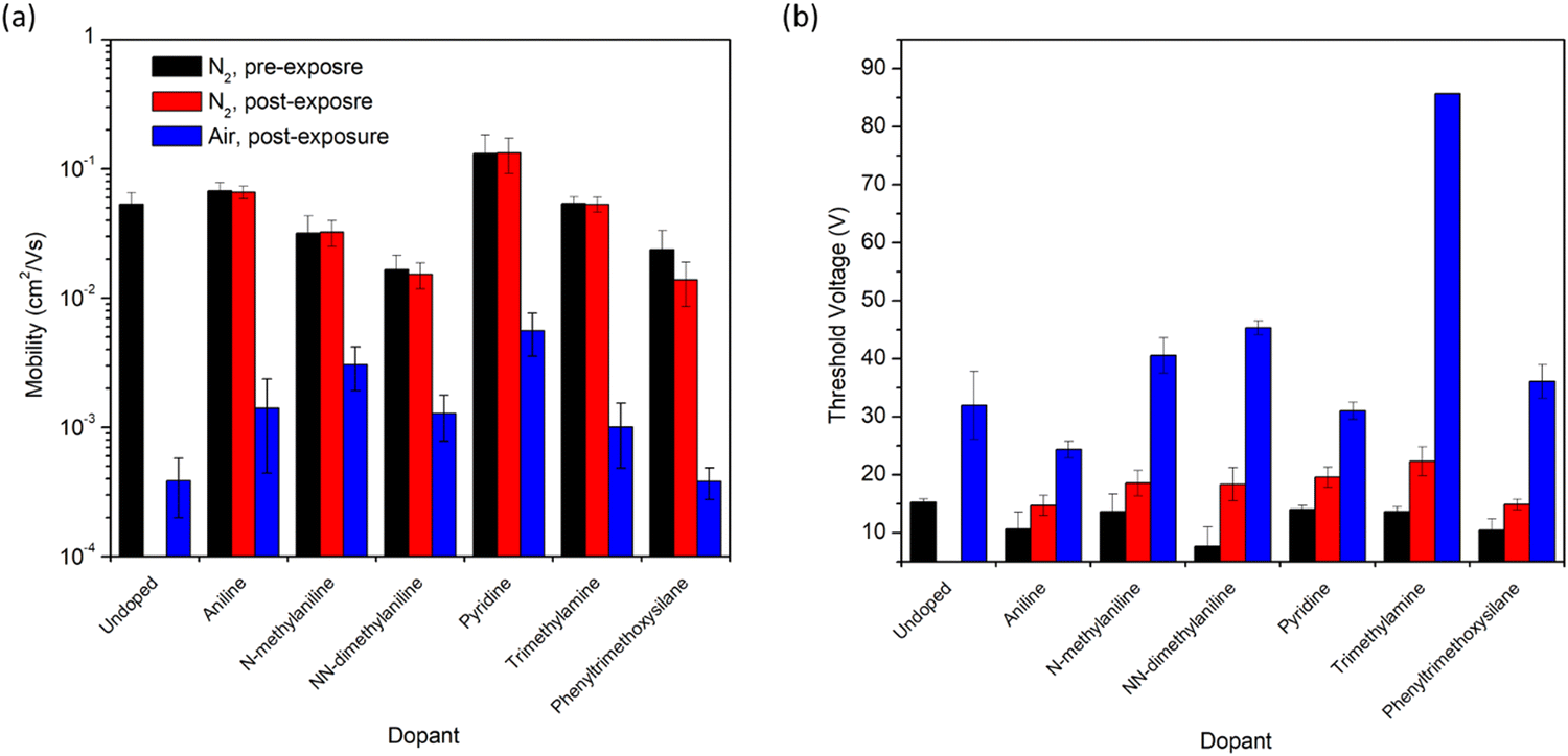 | ||
| Fig. 4 (a) Electron mobility and (b) threshold voltage of devices before and after vapour exposure to amine vapours under inert conditions, and subsequent changes in performance after exposure to air. | ||
The silane with no amine group, phenyltrimethoxysilane, was used to determine the impact of the presence of the silane group in the additives. The use of phenyltrimethoxysilane reduced the μe and increased the VT in nitrogen, but did not impact the device performance in air compared to the control. Silanes are known to be p-type dopants,11 which is consistent with the observed decrease in device performance under N2 in this work. The effect appears reduced in air, indicating either that there are additional interactions between the phenyltrimethoxysilane, oxygen and moisture, or simply that the air exposure has a much more pronounced effect on the P(NDI2OD-T2) device performance compared to the addition of phenyltrimethoxysilane.
The transfer curves (Fig. 5) of the conditions giving rise to the best performance and stability expand on the previous results from Fig. 4. Aniline (Fig. 5b) and pyridine (Fig. 5c) both result in an increased VT after exposure of the device to the vapour, with aniline exhibiting a smaller shift than pyridine. The on-current reached in nitrogen by the films exposed to vapour in both cases is largely unchanged, as a result of the low change in relative μe to the raw P(NDI2OD-T2) film. Both treated films exhibit an increased hysteresis, with aniline resulting in a hysteresis of approximately 5 V and pyridine resulting in hysteresis of about 1 V. In air, both treated films see less shift in VT compared to an untreated sample (Fig. 5a), which contributes to the lower on-current observed in the untreated sample compared to the treated samples. All films display similar hysteresis when exposed to air.
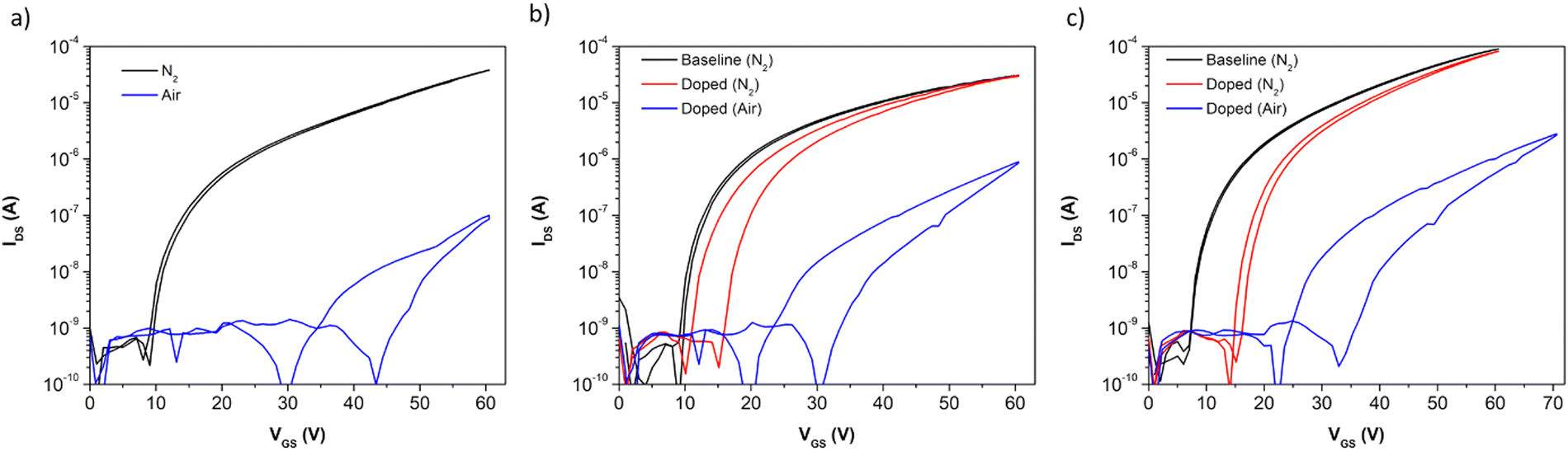 | ||
| Fig. 5 Transfer curves of (a) undoped P(NDI2OD-T2) as a baseline, (b) aniline-doped P(NDI2OD-T2), and (c) pyridine-doped P(NDI2OD-T2) in an N2 glovebox (black, red) and air (blue). VDS = 50 V. | ||
Subsequently, devices were tested after 1 week of exposure to ambient air (Fig. S3, ESI†). Out of 40 devices for each condition, none exhibited functionality after a week of exposure to air, indicating the volatile additives have likely evaporated from the film as expected. This further highlights the importance of developing non-volatile additives for enhancement of device stability. While these devices were not stable after an extended timeframe, these results identify pyridine and aniline as ideal candidates for ideal moieties to include in the design of a non-volatile additive such as a macromolecule.
Finally, to further understand the impact of aniline and pyridine on stability of P(NDI2OD-T2) through changes the material's reduction and oxidation behaviour, cyclic voltammetry was performed. The voltammogram is presented in Fig. 6, where neat P(NDI2OD-T2) is used as the baseline. Films treated with aniline and pyridine exhibit clear differences in redox activity compared to the baseline. When exposed to aniline, an increase of peak separation (ΔEp) for both redox couples was observed. ΔEp,1 and ΔEp,2 for the baseline were both 0.23 V, while they increased to 0.44 V and 0.38 V respectively when exposed to aniline. This increased ΔEp indicates slower transfer of electrons, which may be due to stabilization caused by the presence of aniline. A negative shift of the half-wave potential (E1/2) for redox couple 1 and a positive shift in E1/2 for redox couple 2. E1/2,1 shifted from −1.30 V at the baseline to −1.33 V when exposed to aniline, while E1/2,2 shifted from −0.97 V to −0.92 V. This shift in E1/2 may indicate a difference in redox reactions with oxygen and water present in air, therefore impacting the stability of the devices. When the films were exposed to pyridine, a loss of all redox couples was observed. This may indicate that the pyridine is preventing the transfer of electrons from the films to their environment. Thus, the observed increase in stability of the OTFTs may be due to this change in redox behaviour.
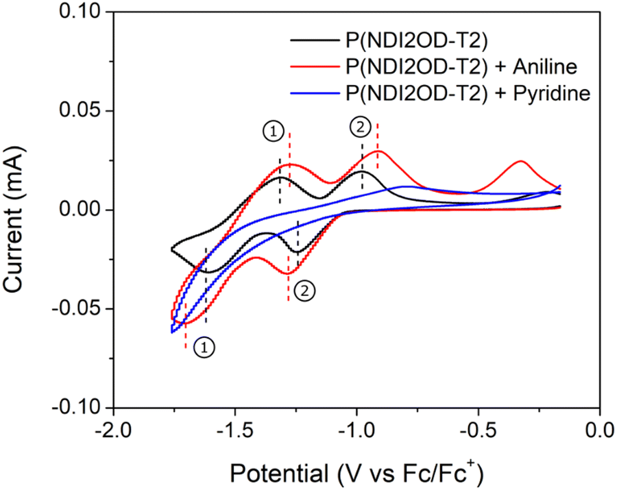 | ||
| Fig. 6 Cyclic voltammogram of neat P(NDI2OD-T2) (black line), and films that have been treated with aniline (red line) or pyridine (blue line). Redox couples (1) and (2) are indicated on the voltammogram for clarity. | ||
Conclusion
Small molecule nitrogen-containing additives such as aniline and pyridine enhanced the stability of P(NDI2OD-T2)-based OTFT devices without degradation of device performance under inert conditions. It appears that increasing the substitution of the amine typically resulted in worse device performance by increasing the VT. However, the use of aromatic nitrogen, such as pyridine, led to a less significant difference compared to the primary amines such as aniline. While previous studies indicated some aminosilane additives could enhance the performance of n-type devices, it was found that of the subset of materials used here, only marginal increases in μe were observed. While this increased μe was retained somewhat in air, increasing the nitrogen content of the silane resulted in the performance in air reverting to behaviour similar to the baseline. The most promising additives from the present study were aniline and pyridine, and these functionalities can be used in the design of further stability enhancing additives.Experimental
Device fabrication
Devices were prepared with batches of 20 transistors on a single substrate, and substrates were prepared in duplicate for a total of 40 individual transistors for each condition. 15 mm × 20 mm Si substrates with thermally grown SiO2 dielectric (220 μm thick) were cleaned sequentially in soapy water, water, acetone, then methanol by sonicating in each solvent for 5 minutes. The substrates were then treated in a Harrick PDC-32G Plasma Cleaner for 10 minutes. After plasma cleaning, substrates were rinsed with water and then isopropyl alcohol, dried by blowing N2 over the substrate, then placed in a solution of 1% (v/v) octyltrichlorosilane (OTS) in toluene for 24 hours. After OTS treatment, the substrates were dried in a vacuum oven at 70 °C for 1 hour. Solutions of P(NDI2OD-T2) were prepared by heating and stirring a 10 mg mL−1 solution in 1,2-dichlorobenzene on a 50 °C hotplate for 20 minutes, then filtering through a 20 μm PTFE filter. These solutions were spin-coated onto the substrates at 4000 rpm for 60 seconds. Films were annealed at 150 °C for 1 hour in a vacuum oven. Gold contact electrodes with chromium interlayers were deposited by physical vapour deposition with a shadow mask for patterning. 10 nm of chromium was deposited at a rate of 0.5 Å s−1, then 50 nm of gold was deposited at a rate of 1 Å s−1. The dimensions of the channel were L = 30 μm and W = 1000 μm.Vapour exposure procedure
Following fabrication, devices were characterized under inert conditions in a N2 glovebox prior to vapour exposure. Inside the glovebox, an open 1 dram vial was placed inside a 20 mL scintillation vial. 20 μL of the desired solvent was pipetted into the 1 dram vial, then the device to be exposed was also placed inside the scintillation vial. The scintillation vial was capped tightly, and the devices were exposed to the vapours of the solvent for 30 minutes. The devices were then re-characterized under inert conditions before moving the samples into air to be subsequently characterized.Transistor characterization
Transistors were characterized with source-drain voltage (VDS) of 50 V, while the gate-source voltage (VGS) was varied from 0 to 60 V and the current measured using a Keithley 2614B source meter. Transistors were characterized in a nitrogen glovebox before and after exposure to the additives. Finally, the transistors were removed from the glovebox and tested again under ambient conditions, where RH was < 10% for all experiments. Saturation region characteristics were extracted as previously reported.13Cyclic voltammetry
Slides of approximately 1 cm × 1.5 cm were cut from ITO-coated glass, then coated with P(NDI2OD-T2) following the spin-coating conditions indicated in the Device Fabrication section. These films were annealed at 150 °C under vacuum for 1 hour. Films exposed to aniline and pyridine were immersed into each solvent for 10 seconds then allowed to dry under ambient conditions for 10 minutes. Voltammograms were obtained using 0.1 M tetrabutylammonium perchlorate dissolved in acetonitrile as the electrolyte. Platinum wires were used for the counter and reference electrode, while the P(NDI2OD-T2)-coated ITO was used as the working electrode. A ferrocene standard reference was also measured, with the same solvent and electrolyte system, and a platinum wire for the working electrode. All voltammograms were normalized to the ferrocene standard.Conflicts of interest
There are no conflicts to declare.Acknowledgements
We thank Natural Sciences and Engineering Research Council of Canada (NSERC, RGPIN-2015-509 03987 to B. H. L.) and NSERC CGS-D (S. B.). The research was undertaken, in part, thanks to funding from the Canada Research Chair program (B. H. L.).References
- R. Po, G. Bianchi, C. Carbonera and A. Pellegrino, “All That Glisters Is Not Gold”: An Analysis of the Synthetic Complexity of Efficient Polymer Donors for Polymer Solar Cells, Macromolecules, 2015, 48, 453–461 CrossRef CAS.
- M. Moser, A. Wadsworth, N. Gasparini, I. McCulloch, M. Moser, A. Wadsworth, I. McCulloch and N. Gasparini, Challenges to the Success of Commercial Organic Photovoltaic Products, Adv. Energy Mater., 2021, 11, 2100056 CrossRef CAS.
- B. Lüssem, C.-M. Keum, D. Kasemann, B. Naab, Z. Bao and K. Leo, Doped Organic Transistors, Chem. Rev., 2016, 116, 13714–13751 CrossRef PubMed.
- I. Salzmann, G. Heimel, M. Oehzelt, S. Winkler and N. Koch, Molecular Electrical Doping of Organic Semiconductors: Fundamental Mechanisms and Emerging Dopant Design Rules, Acc. Chem. Res., 2016, 49, 370–378 CrossRef CAS PubMed.
- F. Zhang, X. Dai, W. Zhu, H. Chung and Y. Diao, Large Modulation of Charge Carrier Mobility in Doped Nanoporous Organic Transistors, Adv. Mater., 2017, 29, 1700411 CrossRef PubMed.
- W. Y. Chou and H. L. Cheng, An Orientation-Controlled Pentacene Film Aligned by Photoaligned Polyimide for Organic Thin-Film Transistor Applications, Adv. Funct. Mater., 2004, 14, 811–815 CrossRef CAS.
- Y. He, J. T. E. Quinn, S. Lee, G. Y. Wang, X. Li, J. Wang and Y. Li, An Aromatic Amine-Containing Polymer as an Additive to Ambipolar Polymer Semiconductor Realizing Unipolar n-Type Charge Transport, Org. Electron., 2017, 49, 406–414 CrossRef CAS.
- M. Nikolka, I. Nasrallah, B. Rose, M. K. Ravva, K. Broch, A. Sadhanala, D. Harkin, J. Charmet, M. Hurhangee and A. Brown, et al., High Operational and Environmental Stability of High-Mobility Conjugated Polymer Field-Effect Transistors through the Use of Molecular Additives, Nat. Mater., 2017, 16, 356–362 CrossRef CAS PubMed.
- N. Shin, J. Zessin, M. H. Lee, M. Hambsch and S. C. B. Mannsfeld, Enhancement of N-Type Organic Field-Effect Transistor Performances through Surface Doping with Aminosilanes, Adv. Funct. Mater., 2018, 28, 1802265 CrossRef.
- B. Sun, W. Hong, E. S. Thibau, H. Aziz, Z.-H. Lu and Y. Li, Polyethylenimine (PEI) As an Effective Dopant To Conveniently Convert Ambipolar and p-Type Polymers into Unipolar n-Type Polymers, ACS Appl. Mater. Interfaces, 2015, 7, 18662–18671 CrossRef CAS PubMed.
- M. F. Calhoun, J. Sanchez, D. Olaya, M. E. Gershenson and V. Podzorov, Electronic Functionalization of the Surface of Organic Semiconductors with Self-Assembled Monolayers, Nat. Mater., 2008, 7, 84–89 CrossRef CAS PubMed.
- N. J. Dallaire, S. Brixi, M. Claus, S. Blawid and B. H. Lessard, Benchmarking Contact Quality in N-Type Organic Thin Film Transistors through an Improved Virtual-Source Emission-Diffusion Model, Appl. Phys. Rev., 2022, 9, 011418 CAS.
- S. Brixi, O. A. Melville, B. Mirka, Y. He, A. D. Hendsbee, H. Meng, Y. Li and B. H. Lessard, Air and Temperature Sensitivity of N-Type Polymer Materials to Meet and Exceed the Standard of N2200, Sci. Rep., 2020, 10, 4014 CrossRef CAS PubMed.
- J. Jakubiak, X. Allonas, J. P. Fouassier, A. Sionkowska, E. Andrzejewska, L. Å. Linden and J. F. Rabek, Camphorquinone–Amines Photoinitating Systems for the Initiation of Free Radical Polymerization, Polymer, 2003, 44, 5219–5226 CrossRef CAS.
Footnote |
| † Electronic supplementary information (ESI) available. See DOI: https://doi.org/10.1039/d3ma00402c |
| This journal is © The Royal Society of Chemistry 2023 |