
 Open Access Article
 This Open Access Article is licensed under a Creative Commons Attribution-Non Commercial 3.0 Unported Licence
Maskless patterning of metal nanoparticles and silicon nanostructures by a droplet deposition and etching process
Chia-Wen
Tsao
 * and
Ping-Chin
Shen
* and
Ping-Chin
Shen
Department of Mechanical Engineering, National Central University, Taoyuan City, Taiwan. E-mail: cwtsao@ncu.edu.tw; Fax: +886-3-4254501; Tel: +886-3-4267343
First published on 18th November 2023
Abstract
This paper introduces a droplet-based method to deposit metal nanoparticles (named: droplet deposition) and etch silicon surfaces creating silicon nanostructures (named: droplet etching). The droplet deposition and etching process is a simple and cost-effective method that only requires a pipette tip for silver and gold nanoparticle coating and fabrication of silicon nanostructures. Besides, it also eliminates the need for mask designs or other fabrication facilities, simplifying the nanoparticle and silicon nanostructure patterning process. For the noble metal nanoparticle coating by droplet deposition, we investigate the influence of various process parameters such as metal ion concentration, hydrofluoric acid concentration, deposition time, and temperature effects on the resulting nanoparticle plating. And for silicon nanostructure creation, we use the droplet etching technique that selectively etches the silicon in regions where metal nanoparticles have been deposited while other regions remain unaffected and well-preserved. Finally, we demonstrate the capability of hand-writing geometric patterning, transferring pre-defined patterns by shadow masking and mass production for droplet deposition and etching using a multi-channel (8-channel) pipette.
1. Introduction
Over the past few decades, the nano-texturing of silicon surfaces has gained significant attention due to its extensive applicability in a variety of fields.1–3 This involves coating metal nanoparticles or creating porous/wire-shaped nanostructures on silicon surfaces. The deposition of the nanoparticle layers typically employs dry deposition facilities like e-beam,4 thermal evaporators,5 or sputtering apparatus.6 And generation of silicon nanostructures can be generally achieved via top-down methods like anisotropic wet chemical etching,7 laser-assisted etching,8 plasma etching,9 reactive ion etching,10 deep reactive ion etching,11 or bottom-up methods, like chemical vapor deposition (CVD),12,13 physical vapor deposition (PVD)14 or laser ablation synthesis15 approaches.While these deposition and etching facilities offer precise control over thickness and uniformity, they are usually costly to acquire and maintain, thereby limiting accessibility for use. As a solution, researchers have proposed the use of simple processes such as electroless plating16 or the metal-assisted chemical etching (MACE)17 process to create metal nanoparticles or silicon nanostructures. Owing to their straightforward and efficient fabrication setups that don’t necessitate the preparation and setup of a galvanic etching cell to generate nanostructured silicon surfaces,18 both electroless plating and MACE have emerged as appealing methods for nanoparticle deposition16 or silicon nanostructure fabrication in various fields including micro-electrical mechanical systems,19,20 biosensors,21,22 solar cells,23,24 energy storage,25,26 mass spectrometry,27,28etc.
Both electroless plating and the etching process typically involve immersing the entire silicon substrate in the plating electrolyte or etching solution. To pattern the metal or silicon nanostructure layer by electroless plating or etching, selective masking techniques can be applied to protect specific areas from coating, resulting in a patterned region on the silicon surface. This is usually done by a standard photolithography,29 electron beam lithography,30 or soft lithography31 process. Nevertheless, these lithography-based techniques typically require lithography facilities or masks to generate the patterns, which can be costly and time-consuming. Alternative maskless techniques for pattern generation, such as using self-assembly,32,33 a magnetic field,34 or direct laser machining35 are being developed to address these limitations. While these techniques offer some advantages, they still require additional steps or specialized equipment. Therefore, there is a need to develop a simple, low-cost method for generating metal nanoparticles or nanostructures.
In this paper, we present a new electroless plating method to deposit silver and gold nanoparticles on a silicon substrate using droplets. Notably, this approach simplifies the process of generating metal nanoparticle patterns on a silicon surface without mask design or other additional steps. To create silicon nanostructures, we utilize this droplet method to locally etch the silicon via an etching process, whereby the etchant selectively etches the metal nanoparticle coated region while leaving other areas protected. In addition to its mask-free advantage, this droplet-based method is more cost-effective, requiring only a small amount of noble metal deposition reagent (a few microliters) and generating less hazardous waste during the process compared to commonly used fully immersive electroless plating methods.
2. Experiment
2.1 Materials and reagents
Hydrofluoric acid (concentration 49%), hydrogen peroxide (concentration 31%), acetone (concentration 100%), and isopropanol (concentration 99.8%) were purchased from BASF Corp (BASF Taiwan, Taipei, Taiwan). Ethanol (concentration 99.5%), methanol (concentration 99.9%), and water (HPLC grade) were purchased from J. T. Baker Chemical Company (Phillipsburg, NJ, USA). Silver nitrate (ACS, 99.9+%, metals basis) and sodium tetrachloroaurate(III) dihydrate (99.99%, metal basis, AU 49–50%) were purchased from Alfa Aesar (MA USA). A boron-doped P-Type wafer (4 inch, single side polished, test grade, resistivity: 1–10 Ohm·cm) was obtained from Advanced Furnace Systems Corp. (Tainan, Taiwan). Prior to metal deposition, the silicon wafer was cut into 1 × 1 cm2 and cleaned with acetone and isopropyl alcohol, followed by rinsing with DI water using an ultrasonic bath to remove the silicon particles and surface contaminants. Gold and silver nanoparticle deposition solutions were prepared by dissolving 28.7 mg tetrachloroaurate(III) dihydrate and 12.3 mg silver nitrate in 26.1 mL HPLC water, respectively, in 3 minutes in an ultrasonic bath, and mixed with 10 mL HF (49%) solution as a deposition reagent. Polydimethylsiloxane (PDMS, SYLGARD™ 184) was purchased from Dow Corning Inc. (Atlanta, GA, USA). SU-8 3050 and SU-8 developer were purchased from MicroChem Corp. (Westborough, MA, USA).2.2 Contact angle measurements
An automatic contact angle measurement system (OCA 15EC, DataPhysics Instruments, Filderstadt, Germany) was used to measure the surface hydrophobicity. In each test, 2 μL water was auto-pipetted onto the silicon surface, and the droplet image was captured and analyzed to calculate the contact angle.2.3 Scanning electron microscope (SEM) image analysis
The SEM images were taken using a Hitachi FESEM (S-4300, Krefeld, Germany) at the Optical Sciences Center at National Central University, Taiwan. All samples were cut into 0.5 × 0.5 cm2 wafers, and attached to the SEM holder to take the top and cross-section images.3. Results and discussion
3.1 Metal nanoparticle plating and silicon nanostructure preparation by droplet deposition
The droplet deposition method is a straightforward process that involves using a pipette to extract a small amount of deposition or etchant solution onto the silicon substrate for the droplet deposition or droplet etching process. We first illustrate the droplet deposition process, shown in Fig. 1. The process begins with a bare silicon wafer and directly pipetting the deposition solution droplet onto the silicon surface. The droplet is left to stay for a couple of minutes, allowing for the electroless plating of noble metal nanoparticles such as Au and Ag onto the silicon surface. Subsequently, the whole substrate is subjected to immersion cleaning in a water beaker to remove the deposited droplets from the silicon surface. It is noted that the quality of the deposition can be directly influenced by the droplet removal process, given that the deposition solution is hydrophilic to the silicon surface at an angle of approximately 35 degrees. In our tests, we attempted to remove the droplet directly by rinsing with water or by drying via N2 gun blowing; but these methods resulted in deposition solution residues leaving deposition marks on the surface. As a result, we opted for the immersion cleaning approach for 5 minutes to rinse the deposition solution from the silicon wafer thoroughly. Finally, the coated substrate is removed from the water beaker, and then N2 blow-dried to complete the nanoparticle plating process. | ||
| Fig. 1 Schematic illustration of the droplet deposition process. | ||
Due to direct contact between the droplet and the silicon surface, the nanoparticle plating patterns become intrinsically correlated with the contact region between the droplet and the silicon wafer. This contact enables selective deposition of nanoparticles onto the contact region, which determines the pattern of nanoparticle plating. To ensure high-quality nanoparticle plating patterns, precise control over the deposition conditions is essential. In the following discussion, we explore the impact of various parameters, including metal ion concentration, temperature, hydrofluoric acid concentration, deposition time, and temperature effects, in order to determine the optimal deposition conditions.
The SEM images in Fig. 2 demonstrate the Ag (a)–(d) and Au (e)–(h) droplet deposition results at varying metal ion concentrations of 1 mM (a), (e), 2 mM (b), (f), 4 mM (c), (g) and 8 mM (d), (h). As the concentration of metal ions increases, the size and coverage rate of deposited metal nanoparticles also increase. The Ag and Au nanoparticle morphology changes with increased concentration. The silver deposition exhibits a three-dimensional dendritic or net-like morphology, while gold deposition tends to grow in a two-dimensional film morphology. Due to the stronger interaction between gold and silicon and heteroepitaxial growth, gold clusters follow the Stranski–Krastanov growth mode. In this mode, gold initially forms two-dimensional planar monolayers.36,37 On the other hand, silver forms small clusters on the surface following the Volmer–Weber growth mode. Due to the agglomeration of silver clusters and strong anisotropic growth, silver follows a diffusion-limited aggregation model to grow and forms three-dimensional dendritic structures.38,39
 | ||
| Fig. 2 ×50k and ×10k (right-bottom) SEM images of silver (Ag) and gold (Au) nanoparticles by droplet deposition with 1 mM, 2 mM, 4 mM, and 8 mM ion concentrations. The HF concentration was 8 M, and the deposition time was 60 seconds. | ||
The particle size distribution and deposition coverage are summarized in Fig. 3. It clearly shows that both the size and surface coverage of deposited metal nanoparticles grow proportionally with increasing ion concentrations. At a low metal ion concentration of 1 mM, the majority of metal nanoparticles are found to be distributed within a 0–1 × 10⁻³ μm2 range. At a high metal ion concentration of 8 mM, there is noticeable growth in large metal particles of both silver and gold, with sizes exceeding 5 × 10⁻³ μm2. Correspondingly, the surface coverage shows an increase from 23.4% to 41% for silver and from 34.5% to 80.1% for gold. This difference is attributed to the distinct surface morphology between Ag and Au, illustrated in Fig. 2. Notably, gold nanoparticles exhibit a tendency to grow laterally under increased ion concentrations, leading to higher deposition coverages compared to silver deposition.
 | ||
| Fig. 3 Particle size distribution percentage (black color y-axis label) and coverage percentage (blue color y-axis label) for Ag and Au nanoparticle deposition with various metal ion concentrations. The particle size distribution % is defined as the ratio of the number of metal particles in each size segment to the total number of metal particles, and the coverage percentage is defined as the ratio of metal coverage area to the total area. | ||
Additionally, the effects of metal ion concentration on deposition times were investigated. The experiments were conducted using three distinct deposition durations of 30, 60, and 90 seconds under conditions of 8 M HF and 4 mM ion concentrations. As displayed in Fig. 4, we observe growth in particle size with time for Ag droplet deposition. Gold exhibits more minor differences in deposition at three different time intervals than silver. This is presumably due to the high deposition coverage of gold; the number of active deposition sites available for metal ion attachment is relatively limited. This leads to a decrease in the deposition rate and shows little effect on Au droplet deposition conditions.
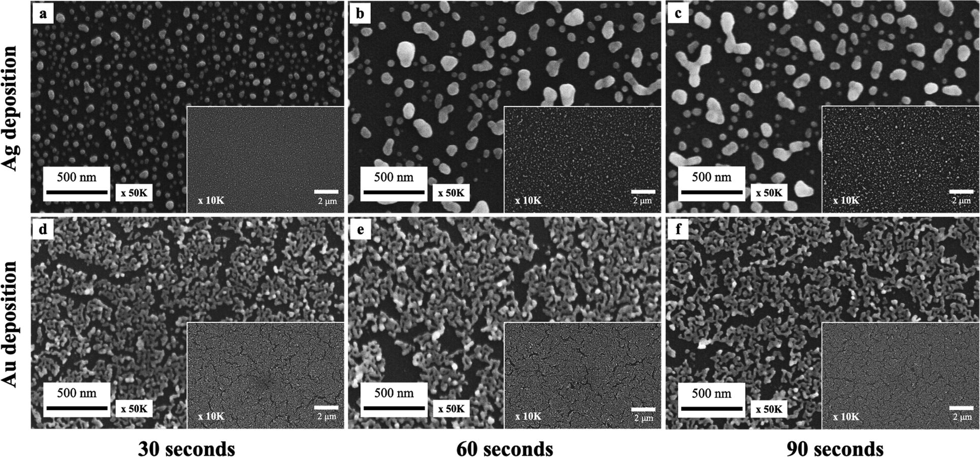 | ||
| Fig. 4 ×50k and ×10k (right-bottom) SEM images of silver (Ag) and gold (Au) nanoparticles by droplet deposition with 30, 60, and 90 seconds. The ion concentration was 4 mM, and the HF concentration was 8 M. | ||
 | ||
| Fig. 5 (a) ×50k and ×10k (right-bottom) SEM images of silver (Ag) and gold (Au) nanoparticles by droplet deposition with 4, 8, and 12 M concentrations. The ion concentration was 2 mM, and the HF concentration was 8 M. Deposition time is 60 seconds. (b) Particle size distribution percentage (black color y-axis label) and coverage percentage (blue color y-axis label) for Ag and Au nanoparticle deposition with various metal ion concentrations. The particle size distribution % is defined as the ratio of the number of metal particles in each size segment to the total number of metal particles, and the coverage percentage is defined as the ratio of metal coverage area to the total area. | ||
 | ||
| Fig. 6 (a) Photographic images of droplet evaporation over time (30–90 seconds) at room and elevated 60 °C temperatures. (b) SEM images illustrating Ag and Au nanoparticle distribution on the silicon surface at room temperature and 60 °C by the droplet deposition method. | ||
Referring to the SEM image depicted in Fig. 6(b), it can be discerned that under room temperature conditions, silver and gold are more uniformly deposited onto the silicon surface within the droplet contact area compared to that under the higher temperature conditions, with the exception of the droplet edge. Conversely, at 60 °C, the deposition droplet evaporates and concentrates towards the center at this elevated temperature, resulting in a higher nanoparticle density at the droplet contact region, while the dried areas exhibit only a minimal nanoparticle presence on the surface. Furthermore, we observed an expansion of the edge etching region in the droplet deposition method as the deposition temperature increased. This phenomenon can be attributed to the reduction in droplet size due to evaporation, causing the dry region to be exposed to hydrofluoric acid etching before complete evaporation. We speculate that droplet evaporation has an adverse effect on droplet deposition, making it more challenging for metal ions to reach the edge region for deposition, resulting in non-uniform metal deposition under high temperature conditions. Therefore, it is important to control the droplet evaporation/condensation on the silicon surface if uniform droplet deposition is required. We suggested minimizing the possibility of droplet evaporation by lowering the deposition temperature or increasing the environmental humidity.
3.2 Nanostructured silicon surface fabrication by droplet etching
Following the deposition of noble metal nanoparticles, we employed MACE to create silicon nanostructures by the droplet etching approach. This process differs from the conventional MACE practice, where noble metal-coated silicon substrates are fully immersed in the etching solution. This droplet etching method offers an advantage for the local etching of Ag/Au-coated regions without causing damage to the uncoated region. The droplet etching is demonstrated in Fig. 7. It begins with the deposition of the HF/H2O2/C2H5OH (volume ratio 5![[thin space (1/6-em)]](https://www.rsc.org/images/entities/char_2009.gif) :1:5) etching solution onto the coated region and staying for a few minutes. Following this, the entire substrate is rinsed with methanol, and subsequently dried using an N2 gun to fabricate the nanostructure pattern on the silicon surface.
:1:5) etching solution onto the coated region and staying for a few minutes. Following this, the entire substrate is rinsed with methanol, and subsequently dried using an N2 gun to fabricate the nanostructure pattern on the silicon surface.
 | ||
| Fig. 7 Schematic illustration of the droplet etching process. | ||
From the SEM images presented in Fig. 8, circular-shape silicon nanostructure patterns are generated by the droplet etching process. The Ag-coated substrate shows 0.1–0.8 μm diameter and 0.6–2.7 μm height pore-shape surface morphology. The Au-coated substrate shows 0.1–0.6 μm diameter and 1.6–1.7 μm height wire-shape surface morphology. For 1 minute etching time, as displayed in Fig. 8(a), the silicon nanostructure morphology, size, and length created by the droplet etching process are similar to those created using the conventional MACE process where the silicon substrate was fully immersed in the etching solution for a short etching time. An important distinguishing feature of the droplet etching process is its ability to confine etching to the Ag/Au-coated regions. This effectively leaves the silicon surface outside the droplet etching region unscathed and protected, ensuring the preservation of the base material's integrity. In contrast, full immersion MACE etching often results in the formation of numerous tiny pits dispersed across substrate areas that are not targeted for etching, as shown in Fig. 8(a). This demonstrates the advantages over the standard MACE process. It effectively prevents silicon surfaces outside the metal deposition area from being damaged by HF etching, making it particularly valuable for applications requiring a high degree of surface flatness, such as silicon bonding. Furthermore, the droplet etching process offers the advantage of selective etching in the desired metal deposition areas without the need for intricate masking techniques to protect the surface from being etched or damaged, which is typically associated with conventional MACE processes.
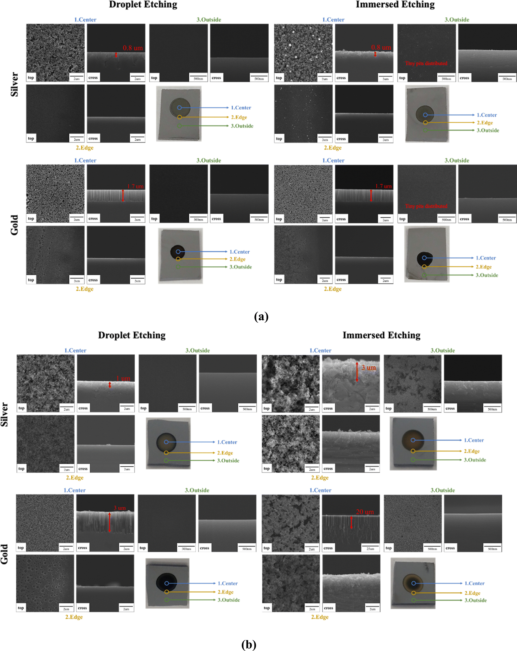 | ||
| Fig. 8 Etching for (a) 1 minute and (b) 20 minutes. The silver and gold nanoparticle coating for this droplet etching test is 8 M HF 2 mM ion concentration, deposition time: 90 seconds, room temp. | ||
When extending the etching time to 20 minutes, as demonstrated in Fig. 8(b), distinct morphological differences become apparent between droplet etching and immersion etching. Although both the Ag- and Au-coated substrates present similar pore and wire-shaped surface morphologies, the immersion method tends to yield larger surface features compared to the droplet etching process. For Ag-coated substrates the pore shape surface was measured to have 0.9–2.1 μm diameter and 3–15 μm height. And for Au coated substrates, the pore shape surface was measured to have 0.8–1.5 μm diameter and 18–44 μm height. Since the droplet etching employs significantly less solution than the immersion method (1 μL compared to ∼200 mL), it is plausible that, with the progression of the reaction, the overall HF and H2O2 concentrations decrease over a long reaction time which decreases the etching rate in a small volume. Therefore, we observed surface morphology difference for more extended etching time conditions.
3.3 Maskless patterning of metal nanoparticles and porous silicon by the droplet deposition method
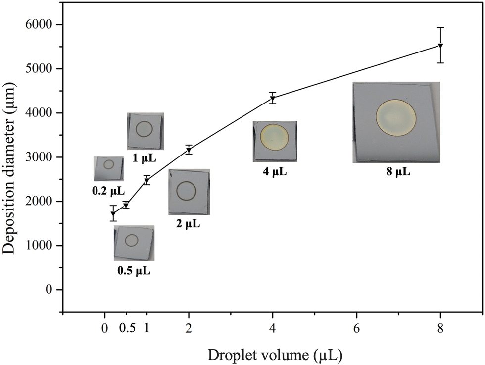 | ||
| Fig. 9 Correlation between droplet volume and resultant pattern size on the silicon surface by droplet deposition. The deposition conditions for this experiment: 8 M HF concentration, 2 mM metal ion concentration, room temperature environment, and 90 seconds deposition time. | ||
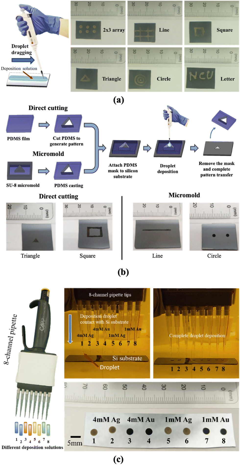 | ||
| Fig. 10 Demonstration of the droplet deposition and droplet MACE etching by (a) hand-writing, (b) using PDMS as a masking layer, and (c) high-throughput patterning (8 patterns) generation with an 8-channel pipette tip. | ||
Another advantage of the droplet deposition method is its compatibility with commercially available droplet deposition systems or pipettes. In our earlier discussions, we utilized a single-channel pipette to examine the influence of various droplet deposition process parameters. However, when larger-scale depositions are required, multi-channel pipette tips can be used to pattern droplet arrays with high throughput. In addition, these tips are not confined to depositing a one-type deposition solution. Instead, each pipette tip can act as an individual deposition site, depositing various conditions on the substrate in a single run. As shown in Fig. 10(c), we demonstrate high-throughput microdroplet deposition using an 8-channel pipette (CAPP C200-8). In this test, the eight droplets contained four different types of deposition solutions (two droplets for 4 mM Ag, 4 mM Au, 1 mM Ag, and 1 mM Au). This allows the deposition of distinct coating reagents on the surface silicon in a single pipette run. These multi-channel approaches presented the flexibility and the scalability of the droplet deposition method marking the droplet deposition/etching method as a potential tool in nanotechnology research.
4. Conclusions
In this research, we have successfully demonstrated a novel methodology for maskless patterning of noble metal nanoparticles and silicon nanostructure fabrication via the droplet deposition and etching process. For the droplet deposition, we investigated various deposition parameters for silver and gold nanoparticle deposition. The results showed that metal ion concentration has a profound impact on nanoparticle deposition; both silver deposition and gold deposition show increasing nanoparticle size and coverage rate with increasing metal ion concentration. Given the droplet's small volume, deposition at room temperature was found to be preferable to ensure a uniform nanoparticle distribution. In contrast, at elevated temperatures above 60 °C, evaporation occurred, leading to a concentrated nanoparticle coating.After nanoparticle deposition, we utilized the droplet etching method to locally etch silicon, creating silicon nanostructure patterns. This localized etching process ensures the protection of uncoated regions, showing another significant advantage of this method. In this study, we selected Ag and Au as noble metals in the proposed droplet-based MACE process to produce high aspect ratio porous silicon microstructures. Other metals such as Pt,41 Cu42 and Ni43 can also applied in this droplet-based approach to generate porous-shape (Pt) and pit or inverted pyramid shape (Cu and Ni) morphologies.
Finally, we use hand-writing and shadow mask methods to create various geometries and patterns on the silicon surface, and also demonstrated that the droplet deposition and etching method is fully compatible with commercially available droplet deposition or pipette systems, including both single-channel and multi-channel (8-channel) pipettes, as demonstrated in this paper. In the future, for industrial-level applications or higher fabrication throughput demands, automated 96/384-well/droplet high throughput electronic pipette systems can be used for more precise, controllable, and mass-produced droplet deposition, creating metal nanoparticles on silicon surfaces or porous silicon patterns for various applications.
Conflicts of interest
There are no conflicts to declare.Acknowledgements
The authors would like to thank the National Science and Technology Council, Taiwan (NSTC), for financially supporting this project (grant number (NSTC 111-2221-E-008-MY3)).References
- F. A. Harraz, Porous silicon chemical sensors and biosensors: A review, Sens. Actuators, B, 2014, 202, 897–912, DOI:10.1016/j.snb.2014.06.048.
- G. J. Zhang and Y. Ning, Silicon nanowire biosensor and its applications in disease diagnostics: A review, Anal. Chim. Acta, 2012, 749, 1–15, DOI:10.1016/j.aca.2012.08.035.
- Y. Yang, et al., A review on silicon nanowire-based anodes for next-generation high-performance lithium-ion batteries from a material-based perspective, Sustainable Energy and Fuels, 2020, 4(4), 1577–1594, 10.1039/c9se01165j.
- A. Khabari, F. K. Urban, III, P. Griffiths, I. Petrov, Y.-W. Kim and C. Bungay, Nanoparticle beam formation and investigation of gold nanostructured films, J. Vac. Sci. Technol., B: Microelectron. Nanometer Struct. – Process., Meas., Phenom., 2003, 21(6), 2313–2318, DOI:10.1116/1.1615985.
- D. Gaspar, et al., Influence of the layer thickness in plasmonic gold nanoparticles produced by thermal evaporation, Sci. Rep., 2013, 3(1), 1469, DOI:10.1038/srep01469.
- N. Baig, I. Kammakakam and W. Falath, Nanomaterials: a review of synthesis methods, properties, recent progress, and challenges, Mater. Adv., 2021, 2(6), 1821–1871, 10.1039/D0MA00807A.
- M. Y. Arafat, M. A. Islam, A. W. B. Mahmood, F. Abdullah, T. S. Kiong and N. Amin, Study of Black Silicon Wafer through Wet Chemical Etching for Parametric Optimization in Enhancing Solar Cell Performance by PC1D Numerical Simulation, Crystals, 2021, 11(8), 881, DOI:10.3390/cryst11080881.
- N. H. Harb and F. A. H. Mutlak, Production and characterization of porous silicon via laser-assisted etching: Effect of gamma irradiation, Optik, 2021, 246, 167800, DOI:10.1016/j.ijleo.2021.167800.
- A. Smyrnakis, E. Almpanis, V. Constantoudis, N. Papanikolaou and E. Gogolides, Optical properties of high aspect ratio plasma etched silicon nanowires: fabrication-induced variability dramatically reduces reflectance, Nanotechnology, 2015, 26(8), 085301, DOI:10.1088/0957-4484/26/8/085301.
- A. D. Refino, et al., Versatilely tuned vertical silicon nanowire arrays by cryogenic reactive ion etching as a lithium-ion battery anode, Sci. Rep., 2021, 11(1), 19779, DOI:10.1038/s41598-021-99173-4.
- Y. J. Hung, S. L. Lee, B. J. Thibeault and L. A. Coldren, Fabrication of Highly Ordered Silicon Nanowire Arrays With Controllable Sidewall Profiles for Achieving Low-Surface Reflection, IEEE J. Sel. Top. Quantum Electron, 2011, 17(4), 869–877, DOI:10.1109/Jstqe.2010.2068540.
- R. A. Puglisi, et al., Chemical Vapor Deposition Growth of Silicon Nanowires with Diameter Smaller Than 5 nm, ACS Omega, 2019, 4(19), 17967–17971, DOI:10.1021/acsomega.9b01488.
- A. Colli, et al., Thermal and chemical vapor deposition of Si nanowires: Shape control, dispersion, and electrical properties, J. Appl. Phys., 2007, 102(3), 034302, DOI:10.1063/1.2764050.
- L. Wang, X. Zhang, S. Zhao, G. Zhou, Y. Zhou and J. Qi, Synthesis of well-aligned ZnO nanowires by simple physical vapor deposition on c-oriented ZnO thin films without catalysts or additives, Appl. Phys. Lett., 2005, 86(2), 024108, DOI:10.1063/1.1851607.
- N. Fukata, T. Oshima, T. Tsurui, S. Ito and K. Murakami, Synthesis of silicon nanowires using laser ablation method and their manipulation by electron beam, Sci. Technol. Adv. Mater., 2005, 6(6), 628–632, DOI:10.1016/j.stam.2005.06.015.
- A. Lahiri and S. I. Kobayashi, Electroless deposition of gold on silicon and its potential applications: review, Surf. Eng., 2016, 32(5), 321–337, DOI:10.1179/1743294415Y.0000000060.
- H. Han, Z. Huang and W. Lee, Metal-assisted chemical etching of silicon and nanotechnology applications, Nano Today, 2014, 9(3), 271–304, DOI:10.1016/j.nantod.2014.04.013.
- X. Li and P. W. Bohn, Metal-assisted chemical etching in HF/H(2)O(2) produces porous silicon, Appl. Phys. Lett., 2000, 77(16), 2572–2574 CrossRef CAS.
- N. Van Toan, X. Wang, N. Inomata, M. Toda, I. Voiculescu and T. Ono, Low Cost and High-Aspect Ratio Micro/Nano Device Fabrication by Using Innovative Metal-Assisted Chemical Etching Method, Adv. Eng. Mater., 2019, 21(8), 1900490, DOI:10.1002/adem.201900490.
- O. J. Hildreth and D. R. Schmidt, Vapor Phase Metal-Assisted Chemical Etching of Silicon, Adv. Funct. Mater., 2014, 24(24), 3827–3833, DOI:10.1002/adfm.201304129.
- R. F. Balderas-Valadez, V. Agarwal and C. Pacholski, Fabrication of porous silicon-based optical sensors using metal-assisted chemical etching, RSC Adv., 2016, 6(26), 21430–21434, 10.1039/C5RA26816H.
- V. Solis-Tinoco, S. Marquez, B. Sepulveda and L. M. Lechuga, Fabrication of well-ordered silicon nanopillars embedded in a microchannel via metal-assisted chemical etching: a route towards an opto-mechanical biosensor, RSC Adv., 2016, 6(88), 85666–85674, 10.1039/c6ra15485a.
- C. Huo, et al., Metal-Assisted Chemical Etching of Silicon in Oxidizing HF Solutions: Origin, Mechanism, Development, and Black Silicon Solar Cell Application, Adv. Funct. Mater., 2020, 30(52), 2005744, DOI:10.1002/adfm.202005744.
- S. D. Wang, S. Y. Chen, S. P. Hsu, C. Y. Liao and W. Y. Hsu, Ag and Cu metal-assisted chemical etching for diamond-wire-sawn single-crystalline silicon solar cell, Appl. Surf. Sci., 2022, 578, 152050, DOI:10.1016/j.apsusc.2021.152050.
- J. H. Li, N. V. Toan, Z. Q. Wang and T. Ono, Metal-assisted-chemical-etching of silicon nanowires for templating 3D graphene growth towards energy storage in microsystems, J. Micromech. Microeng., 2019, 29(5), 055007, DOI:10.1088/1361-6439/ab0b2f.
- W. McSweeney, H. Geaney and C. O’Dwyer, Metal-assisted chemical etching of silicon and the behavior of nanoscale silicon materials as Li-ion battery anodes, Nano Res., 2015, 8(5), 1395–1442, DOI:10.1007/s12274-014-0659-9.
- C. W. Tsao and Z. J. Yang, High Sensitivity and High Detection Specificity of Gold-Nanoparticle-Grafted Nanostructured Silicon Mass Spectrometry for Glucose Analysis, ACS Appl. Mater Interfaces, 2015, 7(40), 22630–22637, DOI:10.1021/acsami.5b07395.
- J. J. Thomas, Z. Shen, J. E. Crowell, M. G. Finn and G. Siuzdak, Desorption/ionization on silicon (DIOS): A diverse mass spectrometry platform for protein characterization, Proc. Natl. Acad. Sci. U. S. A., 2001, 98(9), 4932–4937, DOI:10.1073/pnas.081069298.
- B. H. Liu, F.-Y. Liao and J.-H. Chen, Design, fabrication, and characterization of electroless Ni–P alloy films for micro heating devices, Thin Solid Films, 2013, 537, 263–268, DOI:10.1016/j.tsf.2013.04.136.
- F. Gentile, et al., Electroless deposition of metal nanoparticle clusters: Effect of pattern distance, J. Vac. Sci. Technol. B, 2014, 32(3), 031804, DOI:10.1116/1.4870058.
- H. Lim, J. H. Noh, D. G. Choi, W. D. Kim and R. Maboudian, A simple soft lithographic nanopatterning of gold on gallium arsenide via galvanic displacement, J. Nanosci. Nanotechnol., 2010, 10(8), 5020–5026, DOI:10.1166/jnn.2010.2390.
- S. B. Ulapane, N. J. B. Kamathewatta, A. K. Borkowski, S. J. Steuart and C. L. Berrie, Periodic Silver and Gold Nanodot Array Fabrication on Nanosphere Lithography-Based Patterns Using Electroless Deposition, J. Phys. Chem. C, 2020, 124(28), 15646–15655, DOI:10.1021/acs.jpcc.0c05247.
- S. B. Ulapane, N. J. B. Kamathewatta, H. M. Ashberry and C. L. Berrie, Controlled Electroless Deposition of Noble Metals on Silicon Substrates Using Self-Assembled Monolayers as Molecular Resists To Generate Nanopatterned Surfaces for Electronics and Plasmonics, ACS Appl. Nano Mater., 2019, 2(11), 7114–7125, DOI:10.1021/acsanm.9b01641.
- S. Danilova, J. E. Graves, J. Sort, E. Pellicer, G. W. V. Cave and A. Cobley, Electroless copper plating obtained by Selective Metallisation using a Magnetic Field (SMMF), Electrochim. Acta, 2021, 389, 138763, DOI:10.1016/j.electacta.2021.138763.
- M. Aleem, R. Vishnuraj, B. Krishnan and B. Pullithadathil, Realization of Micropatterned, Narrow Line-Width Ni–Cu–Sn Front Contact Grid Pattern Using Maskless Direct-Write Lithography for Industrial Silicon Solar Cells, ACS Appl. Energy Mater., 2021, 4(10), 10682–10696, DOI:10.1021/acsaem.1c01699.
- R. G. Milazzo, et al., Influence of hydrofluoric acid treatment on electroless deposition of Au clusters, Beilstein J. Nanotechnol., 2017, 8, 183–189, DOI:10.3762/bjnano.8.19.
- S. Y. Sayed, F. Wang, M. Malac, A. Meldrum, R. F. Egerton and J. M. Buriak, Heteroepitaxial Growth of Gold Nanostructures on Silicon by Galvanic Displacement, ACS Nano, 2009, 3(9), 2809–2817, DOI:10.1021/nn900685a.
- J. Fang, H. You, P. Kong, Y. Yi, X. Song and B. Ding, Dendritic Silver Nanostructure Growth and Evolution in Replacement Reaction, Cryst. Growth Des., 2007, 7(5), 864–867, DOI:10.1021/cg0604879.
- F. Gentile, et al., Electroless deposition dynamics of silver nanoparticles clusters: A diffusion limited aggregation (DLA) approach, Microelectron. Eng.g, 2012, 98, 359–362, DOI:10.1016/j.mee.2012.07.041.
- W.-W. Hu, S.-Y. Yang, C.-W. Tsao, S.-L. Chen and C.-Y. Tzeng, Deposition of polypyrrole on wrinkled polydimethylsiloxane to fabricate stretchable conductive membranes for multifunctional bioreactor applications, Prog. Org. Coat., 2023, 181, 107573, DOI:10.1016/j.porgcoat.2023.107573.
- K. Peng, A. Lu, R. Zhang and S.-T. Lee, Motility of Metal Nanoparticles in Silicon and Induced Anisotropic Silicon Etching, Adv. Funct. Mater., 2008, 18(19), 3026–3035, DOI:10.1002/adfm.200800371.
- Y.-T. Lu and A. R. Barron, Anti-reflection layers fabricated by a one-step copper-assisted chemical etching with inverted pyramidal structures intermediate between texturing and nanopore-type black silicon, J. Mater. Chem. A, 2014, 30(2), 12043–12052, 10.1039/C4TA02006E.
- K. Gao, et al., Fabrication of black silicon by Ni assisted chemical etching, Mater. Res. Express., 2018, 5(1), 015020, DOI:10.1088/2053-1591/aaa1fb.
| This journal is © The Royal Society of Chemistry 2023 |