
 Open Access Article
 This Open Access Article is licensed under a Creative Commons Attribution-Non Commercial 3.0 Unported Licence
Cavity structured S-NiO with improved energy density for aqueous asymmetric hybrid supercapacitors by CDA mechanism†
Pratik Ashok
Patil‡
 a,
Suraj Anandrao
Khalate
b,
Umakant Mahadev
Patil
b,
Rajendra Devidas
Kale
a and
Sachin Babasaheb
Kulkarni‡
*a
a,
Suraj Anandrao
Khalate
b,
Umakant Mahadev
Patil
b,
Rajendra Devidas
Kale
a and
Sachin Babasaheb
Kulkarni‡
*a
aAdvanced Electrochemical Laboratory, Department of Physics, Tuljaram Chaturchand College, Baramati (MH), 413102, India. E-mail: sachinkulkarni21@gmail.com
bCentre for Interdisciplinary Research, D. Y. Patil Education Society, Kolhapur-416 006, India
First published on 6th September 2023
Abstract
Recently, hybrid supercapacitors have gained high recognition due to their improved energy density performance without affecting their power density. In this work, sulfur-doped nickel oxide (S-NiO) honeycomb nanostructure electrodes were prepared via a cost-effective chemical bath method through a Capping, Doping and Annealing (CDA) mechanism for Aqueous Asymmetric Hybrid Supercapacitors (AAHSc). The structural, elemental, morphological and electrochemical analysis of S-NiO as a positive electrode is explored in detail. After annealing, an amorphous to crystalline transformation of NiO was observed with a cubic structure owing to the honeycomb like morphology for optimum 1.42 atomic % sulfur doping. The CDA mechanism played a beneficial role in a synergistic process to prepare the S-NiO electrode with enhanced electrochemical properties for supercapacitor performance, exhibiting 71% capacitive current contribution. This optimized S-NiO electrode exhibited a remarkable specific capacitance (791.67 F g−1 at a scan rate of 20 mV s−1) in 1 M KOH aqueous electrolyte. Graphite used as a negative electrode in the AAHSc device configuration (S-NiO//KOH//Graphite) showed a significant specific capacitance of 77.69 F g−1 at 5 mA cm−2 current density in a wide operating potential window of 1.8 V. The AAHSc device delivered a high energy density of 34.96 W h kg−1 at a power density performance of 2567 W kg−1 and 19.36 W h kg−1 even at a high-power density of 7180 W kg−1 for 5 mA cm−2. More remarkably, 91% capacity retention with 81% coulombic efficiency was observed after 6,000 stability cycles at 5 mA cm−2. The current work signifies the great potential of the S-NiO//KOH//graphite device in promoting and emphasising the development of a low-cost new approach towards hybrid energy storage materials.
1. Introduction
The new era of energy storage devices requires portable, lightweight and cost-effective energy sources. Recently, much attention has been focused on developing hybrid supercapacitor devices with high energy-power density, long cycling life and safe operation to curtail energy crises.1–4 It is essential to develop stable and highly efficient electrodes, such as 3D graphene, carbon nanotubes, carbon fibre, RuO2, polymers etc. However, the materials, as well synthesis methods and techniques, are very expensive.5 Current issues with supercapacitors restricting their practical application are relatively low capacitance due to limited active surface area and intrinsic supercapacitive behaviour of the electrode.6 Coated multiple layers involve a polymer gel electrolyte with a different interface between the layer and coated configuration, which reduces the transport of ions by increasing the contact resistance and restricting the cathode to anode charge flow. This unwanted spacing can disintegrate various layers and reduces the effectiveness of the device.7 Although supercapacitors are the most promising energy-storage devices with long cycle life and high-power supply, they are lacking in terms of high energy density.8–10 Many researchers have attempted to make up for the lack of development of new electrode materials.11,12 Herein, a successful attempt has been made to increase the energy and power density of the device at a wide operating potential window by a hybrid strategy through aqueous asymmetric supercapacitors. Additionally, aqueous electrolytes are inexpensive, non-toxic and safe to handle, having high ionic conductivity and mobility.13At present, numerous transition metal oxides are being investigated as electrode materials due to high theoretical specific capacitance as compared to conducting polymers and porous carbon materials.14,15 In particular, the role of sulfur, with a lower electronegativity than oxygen, demonstrates narrow bandgap and high conductivity for transition metal sulfides.16,17 The widely known transition metal oxides (TMOs: ZnO, RuO2, MnCo2O4, V2O5, Fe3O4),18–22 transition metal hydroxides (TMHs: Mn(OH)2, Co(OH)2, Mo(OH)2, Ni(OH)2),23–27 and transition metal sulfides (TMSs: CuS, MoS2, NiS)28–30 are potential materials for electrode design concerning electrochemical energy storage. High redox activities and reversibility make a pseudocapacitive material a promising electrode in supercapacitor design. Pseudocapacitive materials such as NiO have high theoretical capacitance (2584 F g−1), natural abundance, and high thermal stability, with excellent electrochemical properties.31 Nanosheet based mesoporous NiO microspherical structures were synthesized by Lee et al., having a specific capacitance of 403 F g−1 after 1000 charge discharge cycles.32 Yu et al. synthesized hollow sphere nanosheet NiO, exhibiting capacitance of 600 F g−1 after 1000 cycles at 10 A g−1.33 Yuan et al. showed that NiO nano/micro superstructures deliver a specific capacitance of 710 F g−1 at 1 A g−1 and with retention of 98% after 2000 cycles.34 However, the development of NiO structures for high electrochemical performance supercapacitor electrodes is extremely tricky. Paravannoor et al. prepared NiO nanowires by a hydrothermal route and observed a specific capacitance of 750 F g−1 with 88% retention after 1000 cycles.35 On the other hand, efforts are being made to increase the electrochemical performance of electrodes via composites, doping, and the involvement of conductive additives (like active materials with porous current collectors)36,37 using many methods such as hydrothermal electrodeposition, chemical bath deposition, etc, in which current collectors provide abundant electro active sites to assist rapid faradaic redox reactions.38–40 NiO nanoflake arrays synthesised by Yan et al. using the hydrothermal technique showed specific capacitance of 400 F g−1 at 2 A g−1, and capacitance retention of 428 F g−1 was observed after 5000 cycles.41 Wu et al. synthesised NiO-attached graphene oxide owing specific capacitance of 569 F g−1 at 1 A g−1 with ∼80% capacitance retention after 3000 charge discharge cycles.42 Zhao et al. used graphene oxide (GO) directly to fabricate a composite material with 2D graphene/NiO, showing a specific capacitance of 525 F g−1 at a current density of 200 mA cm−1, and capacity retention of 95.4% can be maintained after 1000 cycles.43 Ji et al. synthesised polypyrrole encapsulated flower-like NiO by a hydrothermal route, which exhibited a specific capacitance of 595 F g−1 at 1 A g−1 and 80.7% capacitance retention for 1000 cycles.44 Meanwhile, the synthesis of S doped NiO as active materials can effectively improve material properties. Guai et al. demonstrated sulfur doped NiO thin film as an alternative to Pt for dye-sensitized solar cells (DSSC) applications.45 Therefore, sulfur doping may considerably alter the electrochemical characteristics of NiO towards a reliable positive electrode material for supercapacitors. An ultrathin sulfur-doped NiO spherical nanosheet electrode was synthesized by Singu et al. with acetylene black and a polyvinylidene fluoride (PVDF) binder for redox supercapacitors using SDS as an anionic surfactant and structure-directing agent. They reported a capacitance of 313 F g−1 at a scan rate of 5 mV s−1 in 1 M KOH with almost 99% capacity retention after 1000 charge–discharge cycles.46
In this work, the aim is to achieve a high potential charge storage device with a hybrid approach cost effectively via a simple chemical bath method. Herein, S-NiO deposition is controlled through a Capping, Doping and Annealing (CDA) mechanism on stainless steel substrates for optimum electrochemical execution. The amount of ammonia solution (capping agent) in the bath is varied, and 10, 20 and 30 mL are used for the as-synthesized samples (without annealing) S1, S2 and S3, and annealed samples A1, A2 and A3, respectively. In this study, the A1 electrode achieved superior electrochemical performance compared to the other electrodes with a specific capacitance of 791.67 F g−1 at a 20 mV s−1 scan rate and 766 F g−1 for a current density of 0.8 mA cm−2 in aqueous 1 M KOH. Furthermore, an aqueous asymmetric hybrid supercapacitor (AAHSc) device configured using A1 as a positive electrode and graphite as a negative electrode in the S-NiO//KOH//graphite form is a potential candidate for energy storage. Thus, we report a hybrid approach of surface development through CDA to realize a synergetic effect and superior high-energy electrochemical performance of S-NiO//KOH//graphite through a wide potential.
2. Experimental
2.1 Materials and method
The S-doped nickel oxide nanostructure was prepared using low-cost chemical bath deposition (CBD) via homogenous precipitation. Nickel sulphate (hexahydrate) extra pure [NiSO4·6H2O] and thiourea 99% AR [CH4N2S], were used as precursor sources of nickel and sulfur. Ammonia solution 30% AR/ACS [NH4OH] was used as the capping agent for cation complexation. All the chemicals were of analytical grade obtained from Loba Chemie Ltd without any further purification. A stainless-steel (SS) substrate (4 × 1 cm2, 304 grade) was used as the conducting substrate for deposition. Substrate cleaning was carried out by polishing with zero grade polish paper and rinsing thoroughly with double distilled water.2.2 Formation of S-NiO/SS electrode and reaction mechanism
The synthesis processes of the S-NiO/SS electrode are schematically illustrated in Fig. 1., and include mainly three steps. First, 0.1 M NiSO4·6H2O solution is prepared for a 25 mL bath using double distilled water (DDW). In the capping step, the amounts of liquor ammonia (NH4OH) added to the Ni precursor solution are 10 mL, 20 mL, and 30 mL, resulting in strong complexation of Ni ions for controlled release through reaction kinetics. Through van der Waals forces, amine capped metal ions easily get adsorbed on the heterogeneous surface of the substrate, represented by following reaction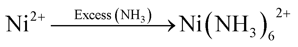 | (1) |
 | ||
| Fig. 1 Schematic illustration of the deposition of nanostructured honeycomb S-NiO on an SS substrate through the three-step CDA mechanism by successful CBD method. | ||
Second, in the sulfur doping step, another bath of 0.1 M thiourea (CH4N2S) solution as a source of sulfur is prepared in 25 mL DDW, and both the solutions are mixed thoroughly by constant stirring on a hot plate. Thiourea as an organic sulfur source has diverse advantages of flexibility and structure-shape diversity to control the nucleation and growth. The bath temperature (80 °C) supplies energy to break the complex and release Ni ions for reaction in a basic bath with a smaller extent of sulfur dissociation from thiourea. Thus, S2− can be released controllably from the organic sulfur source, supplying favourable conditions for the nucleation-growth and accordingly, the structural and morphological modification occurs. Furthermore, well cleaned conducting SS substrates are immersed in the reaction bath for deposition. A heterogeneous reaction occurred during the precipitation and dark greyish deposition takes place on the substrate surface shown by the following reaction:
 | (2) |
The deposited films on the SS were repeatedly washed with DDW. Finally, in the annealing step, as-synthesized samples are subjected to post heat treatment at 300 °C for 3 hr to remove hydrous content, and dark brownish S-NiO/SS electrodes are obtained, as shown by the following reaction:
 | (3) |
The quantity of ammonia (i.e. the degree of complexation) in the bath was varied, and 10 mL, 20 mL & 30 mL were assigned to as-synthesised S1, S2 & S3, and annealed S-NiO/SS A1, A2 & A3 sample electrodes, respectively.
2.3. Characterization techniques
The structures of the samples were characterized by X-ray diffraction (XRD) on a Rigaku Ultima diffractometer using Cu-Kα radiation (λ = 1.54 Å). The morphology was characterized by field emission scanning electron microscopy (FE-SEM, Mira-3, Tescan Pvt. Brno-Czech Republic). Energy dispersive analysis (EDS) measurements were carried out on an Oxford Instrumentations system, inbuilt with FE-SEM. The chemical structure and various oxidation states of S-NiO were examined by an X-ray photoelectron spectroscopy (XPS, PHI 5000 Versaprobe II) system.All electrochemical measurements were performed by a ZIVE MP1 electrochemical workstation. The supercapacitive performance was analyzed by forming a three-electrode electrochemical cell setup with a platinum plate as a counter electrode, an S-NiO electrode as a working electrode and a saturated calomel electrode (SCE) as a reference electrode. Electrochemical studies were carried out by using cyclic voltammetry (CV), galvanostatic charge discharge (GCD) and electrochemical impedance spectroscopy (EIS) tests in 1 M KOH aqueous electrolyte.
3. Results and discussion
3.1 Structural analysis
To undertake a crystallographic study of the thin films, XRD measurements were recorded in the range of 10°–80°. All as-synthesized samples exhibited amorphous nature as shown in Fig. S1 (ESI†). From Fig. 2(a) it is clearly observed that for the annealed samples, remarkable diffraction peaks in the XRD patterns at 2θ° of ∼37.26°, 43.75°, 62.81°, and 79.31° indicate successful NiO formation with (1 1 1), (2 0 0), (2 2 0) and (2 2 2) planes, respectively. These diffraction peaks are in good agreement with the JCPDS card no. 47-1049, Fm3m (225), a = 4.1771 nm. | ||
| Fig. 2 X-Ray diffraction patterns of (a) S-NiO thin films, and (b) magnified portion highlighting the peak shift. | ||
Some intense diffraction peaks observed at 2θ of 44.58°, 51.38° and 75.30° are ascribed to the SS substate and indicated by asterisks (*). The results clearly showed that the impurity peaks were absent, and there was a small extent of sulfur substitution in the NiO lattice sites in the annealed samples. It is clearly confirmed that the annealing process reformed as synthesised amorphous samples into samples with good crystallinity. It is noticed in Fig. 2(b) that there is a decrease in sulfur content with an increase in capping, i.e. degree of complexation. The peak broadenings, i.e. FWHM values, are noticeably found to increase, which indicates crystallite size reduction from A1 to A3. Also, there is marginal peak shifting towards smaller angles, thereby confirming the effect of S-doping from XRD analysis. Chang et al. and Li et al. found the same effect of sulfur doping, resulting in XRD peak shifting at smaller angles, in good agreement with our results.47,48 The average crystallite size of the sample decreases from A1 to A3 with a higher degree of ammonia complexation and decrease in sulfur content given by Debye–Scherrer's equation. Similar results were obtained by Yang et al. and Diallo et al.49,50 Crystallite size, dislocation density, microstrain, band gap values, etc. for A1, A2 and A3 are summarized in Table ST1 (ESI†).
The energy storage capacity of materials has been influenced by the deformation mechanism and dislocation.51 The A1 electrode exhibited the lowest dislocation density and microstrain compared to A2 and A3, which is a sign of good energy storage capacity. With a high degree of capping, the doping of sulfur decreases and results in a reduction in the crystallite size with an increase in the dislocation density, micro-strain, and inter-planar spacing.52 A1 has excess sulfur as compared to the A2 and A3 electrodes, which is why the dislocation reduces. Similar observations have been previously reported concerning the reduction of dislocation due to sulfur doping.53,54
3.2 Morphological and elemental analysis (FESEM and EDS)
Investigation of surface morphology and elemental analysis for as-synthesised and annealed thin samples were carried by FESEM and EDS. The morphologies of the as-synthesized amorphous samples (S1, S2 and S3) revealed undistinguished fuzzy nanoflake like morphology with a lower thickness, as shown in Fig. S2 (ESI†). However, the annealed crystalline electrodes in Fig. 3(a1) and (a2) show the morphology of the A1 sample featuring cavity surfaces looking like a honeycomb structure. A high degree of complexation resulted in the distribution of fewer Ni ions and resulted in the deviation of the morphology from a honeycomb like to a flake like nanostructure, with a change in dimensions, as shown in Fig. 3(b1), (b2) and (c1), (c2). The insets of Fig. 3(a3), (b3) and (c3) clearly show the elemental analysis (% of Ni, O and S) of the S-NiO A1, A2 and A3 samples. It is observed that the nickel and sulfur content along with oxygen vacancies decrease with a greater degree of capping. Table ST2 (ESI†) shows the at% of elements for all samples. Sample A1 is Ni rich (41.03 at%) with high sulfur (1.42 at%) and more oxygen vacancies, i.e. lower oxygen content (57.55 at%) than the A2 and A3 samples. A high capping bath releases less Ni during the reaction due to heavy complexation affecting the growth kinetics and vice versa. | ||
| Fig. 3 FESEM morphologies, EDS spectra and histogram measurements for samples A1 ((a1)–(a4)), A2 ((b1)–(b4)) and A3 ((c1)–(c4)). | ||
Fig. 3(a4), (b4) and (c4) show histograms for the average length and breadth of nanostructured samples A1, A2 and A3, respectively. For A1 the honeycomb wall has average length and breadth of 373.33 ± 9.34 nm and 39.88 ± 6.61 nm. The annealing process is popular to modify morphology, enhancing crystallinity and other structural properties.55,56 The effect of annealing on the growth morphology for the S1 electrode, from a fuzzy to a sturdy honeycomb like structure (with more active sites and large surface area of cavities) is schematically shown in Fig. S3 (ESI†). Sharma et al. developed NiO thin films and observed that annealing resulted in increased crystallinity and affected surface morphology.57 Such a honeycomb like morphology has multiple active sites to increase the specific capacitance.58 Also, ammonia is important to achieve superficial morphology. Deng et al. observed precipitation that means morphology is controlled by the ammonia concentration.59 A facile ammonia influence has been used to grow nanoporous NiO films with a well-defined unique porous structure.60 Also, crystallinity and particle size of NiO improved when using ammonia capping.61 Furthermore, a flower-like structure is credited to ammonia decomplexation.62
Fig. 3(b1)–(b4) showing the A2 electrode, demonstrate a nano-flake structure. The drastic morphology change of the honeycomb like structure into nano-flakes is due to higher complexation and lower sulfur (1.05 at%) doping. Fig. 3(b4) shows the average length and breadth of the nano-flakes to be 393.12 ± 11.07 nm and 41.66 ± 5.95 nm, as evaluated from the histogram for the A2 electrode. Fig. 3(c1)–(c4) reveal that the A3 electrode with the same nano-flake structure exhibits smaller length-breadth and thickness with sizes of 351.95 ± 8.21 nm and 32.04 ± 4.66 nm. A higher degree of capping resulted in a small decrease in sulfur (1.01 at%) content for A3. Furthermore, the at% values of Ni corresponding to the A1, A2 and A3 electrodes are 41.03, 37.63 and 37.25%, respectively. This conclusively indicated that the A1 electrode has the highest wt% and at% of the Ni sites, which are actively involved in the redox mechanism, along with sulfur content, compared to the other samples as shown in Table ST2 (ESI†).
3.3 X-Ray photoelectron spectroscopy (XPS)
The valence information and surface chemical composition of constituent elements in the synthesized S-NiO were examined by X-ray photoelectron spectroscopy (XPS). The broad survey spectrum and high-resolution XPS spectra of Ni 2p, O 1s and S 2p levels are shown in Fig. 4. The wide survey scan spectrum (Fig. 4a) again suggests the presence of Ni, O and S elements, which is consistent with the above EDS result.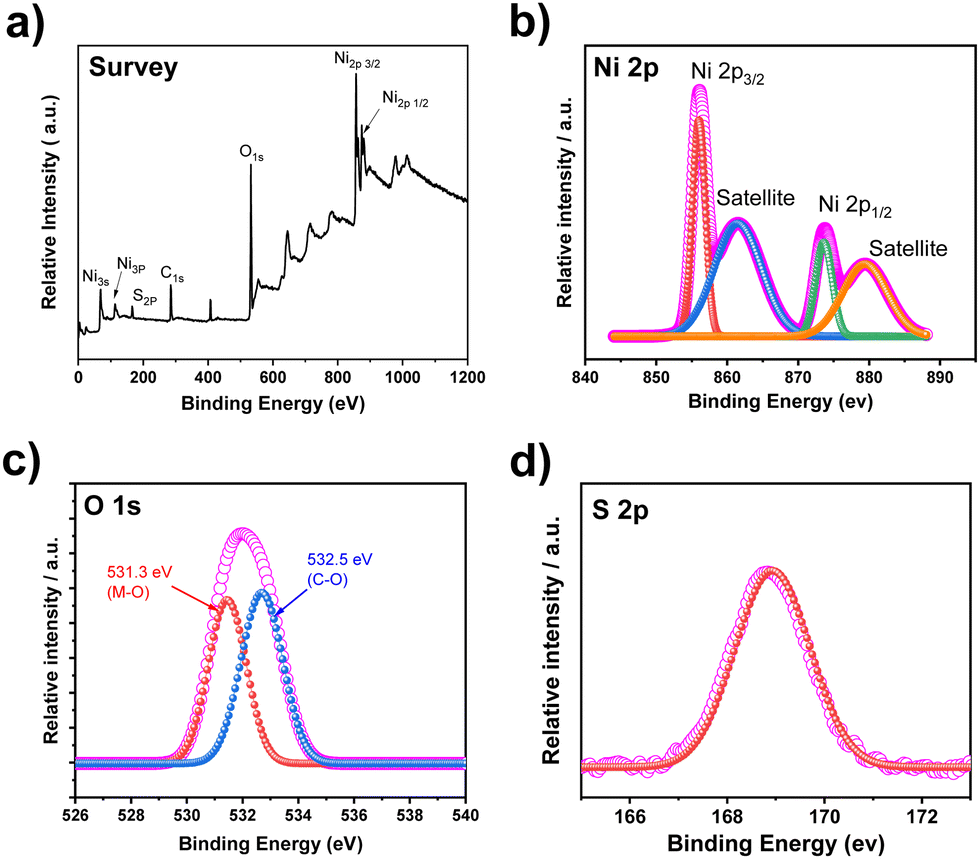 | ||
| Fig. 4 (a) XPS wide survey spectrum of S-NiO, and high-resolution spectra of (b) Ni 2p, (c) O 1s and (d) S 2p. | ||
The high-resolution spectra of the Ni 2p states as revealed by Fig. 4(b) show two prominent peaks with binding energies of 855.6 eV and 873.4 eV, indicating two spin–orbit doublets of Ni 2p3/2 and Ni 2p1/2.63 The difference between these two energy bands is around 17.8 eV, strongly confirming the presence of divalent nickel ions. The O1s states of S-NiO are shown in Fig. 4(c). The O1s spectrum is deconvoluted into two peaks. The first peak was located at 531.3 eV representing the O1s spectra of the metal oxygen bond (M–O) i.e. NiO, and the second peak was located at 532.5 eV, indicating the surface hydroxyls/C–O bond.64 The sulfur core spectrum level of S-NiO is shown in Fig. 4(d). The sulfur S 2p peak was located at 168.9 eV. A similar result was reported by Singu et al.46 The prominent peak over 168 corresponds to the S–O bond.65 These XPS results collectively support the successful formation of S doped NiO nanosheets.
3.4 Electrochemical properties
CDA influenced structural, morphological and elemental electrode characteristics were further investigated for supercapacitive performance with a three electrode system in 1M KOH electrolyte. Cyclic voltammetry (CV), galvanostatic discharge (GD) and electrochemical impedance spectroscopy (EIS) tests were employed for comparative analysis of as synthesized and annealed electrodes as shown in Fig. S4 (ESI†). The as-synthesized samples showed small area CV curves excluding major noticeable redox peaks. However, the annealed samples showed improved electrochemical reactions with distinct redox peaks in large area CV curves. The A1 electrode showed more significant electrochemical performance than the other samples. This comparison significantly highlights the substantial influence of the CDA mechanism in a synergetic way. The optimum capping gives the Ni rich active content of the crystalline S-NiO electrode more oxygen vacancies, improved electrical conductivity and a honeycomb like nanostructure, facilitating more active surface area/sites, accomplishing the major requirements for an efficient supercapacitor electrode with enhanced electrochemical properties as shown in Fig. 5(a). Fig. 5(b) shows the scan rate dependent performance of the optimized A1 electrode. As the scan rate increases, the peak current also increases with peak shifting at higher potential, indicating good reversibility of the fast charge–discharge response. The apparent redox peaks revealed faradaic reactions occurring on the S-NiO surface (active Ni content i.e. Ni2+ ↔ Ni3+) attributed to major capacitance contribution. The walls and surfaces of the cavities in the honeycomb like structure assist more electrolyte storage, leading to substantial charge accumulation. In this study, faradaic redox reaction involves adsorption/desorption of hydroxyl (OH−) ions at the S-NiO/electrolyte interface given by the following eqn (4). | (4) |
 | ||
| Fig. 5 (a) Comparative CV curves for electrodes A1, A2 and A3 in aqueous 1 M KOH at a scan rate of 100 mV s−1. (b) CV curves for the optimized A1 electrode at various scan rates from 2 to 100 mV s−1. (c) Comparative GD curves for electrodes A1, A2 and A3 at 1 mA cm−2. (d) GD curves for the optimized A1 electrode at various current densities of 0.8 to 5 mA cm−2. (e) Comparative EIS (Nyquist) plots for electrodes A1, A2, and A3. (f) Log of current density vs. log of scan rate plots. Comparative current contribution fractions at 100 mV s−1 with inset graphs showing attribution to capacitive and diffusive charge storage for the (g) A1, (h) A2 and (i) A3 electrodes. | ||
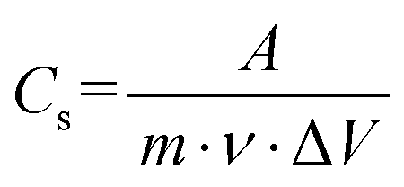
In particular, the amount of sulfur in NiO can increase the number of electrochemically active sites, which can lead to increased interfacial dynamics by the honeycomb like structure. The specific capacitance of the electrodes was calculated from the CV curve by using equation 5:
 | (5) |
 , m is the active mass loaded on the sample, ν is the scan rate, and ΔV is the operating potential window. The calculated specific capacitance values at 20 mV s−1 for the A1, A2 and A3 electrodes are 791.67 F g−1, 515.41 F g−1 and 305.76 F g−1, respectively. The specific capacitance decreases with increasing capping concentration due to the slower release of Ni ions for A2 and A3. Thus, less active Ni and sulfur incorporation with oxygen deficiencies was observed than for the A1 electrodes. The shifting in the redox peaks with respect to increasing scan rate was mainly due to the increasing internal diffusion resistance and we remain successful at decreasing the internal diffusion because of the richness in active Ni with sulfur content.66,67 The annealing process has a favourable effect on redox activity as shown in Fig. S5 (ESI†).
To investigate the fast discharge ability and better stability, the galvanostatic curve was tested in 1 M KOH electrolyte for all samples as shown in Fig. S6 (ESI†). Fig. 5(c) shows the galvanostatic discharge (GD) curves of A1, A2 and A3 electrodes at 1 mA cm−2. Both the GD curves for A2 and A3 marginally overlap due to similar kinds of morphologies along with approximately comparable incorporation of Ni active and sulfur content prepared at a high degree of complexation (Table ST2, ESI†). Fig. 5(d) shows GD curves for the optimised A1 electrode at various current densities ranging from 0.8 to 5 mA cm−2. The discharge time decreases with increase in current density. The A1 electrode achieved a large discharge time at a lower current density value. The honeycomb like structure with appropriate Ni and S contents of the A1 sample facilitates ion transfer, contributing to high and stable specific capacitance at high current densities. Thus, the A1 electrode exhibited high specific capacitance, calculated by eqn (6):
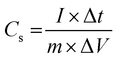 | (6) |
Electrochemical impedance spectroscopy (EIS) was employed for detailed investigation of all electrodes shown in Fig. S7 (ESI†). Fig. 5(e) shows Nyquist plots in a frequency range from 0.01 Hz to 10 kHz at open circuit potential (OCP), and the inset shows a magnified view along with the equivalent circuit for the A1, A2 and A3 electrodes. Here Z′ and Z′′ are the real and imaginary parts of the impedance. The high and low frequency regions are associated with a semicircle and vertical sloping straight line, respectively. The A1 electrode has a vertical sloping straight line at the low frequency region and a smaller depressed arc at the high frequency region, indicating a decent capacitive storage mechanism and lower polarization resistance than the A2 and A3 electrodes. The solution resistance (Rs), polarization resistance (Rp) and constant phase element (CPE) of the A1, A2 and A3 electrodes were determined by fitting the data with the equivalent circuit and the comparative values are tabulated in Table ST3 (ESI†). Rs values for the A1, A2 and A3 electrodes are found to be 0.93, 0.91 and 0.90 Ω, respectively, and the Rp values are 0.45, 0.97 and 1.10 Ω, respectively. It is observed that the Rs values for all samples are close and the A1 electrode showed the lowest Rp value. The interface of A1 has a honeycomb like structure, which stimulates electrochemical reaction through active surface cavities with ease for diffusion of electrolyte ions. Thus, exclusive lattice structures of A1 with great crystallinity, provided by the CDA mechanism, can be responsible for excessive reaction active sites along with appropriate doping and oxygen vacancies of the Ni rich electrode boosts electrical conductivity to promote practicable pathways for the rapid electron transfer with reduction in Rp. In summary, the CDA mechanism results in improved electrochemical performance of the S-NiO electrode as shown in Fig. S8 (ESI†) in comparison with undoped NiO.
In CV measurements, the relationship between response current (i) and scan rate (ν) is crucially significant to interpret the slow diffusion-controlled process (idiff) and fast faradaic reactions on the electrode surface (icap), given by the empirical equation
| i(v) = avb i.e. |
| i(v) = icap + idiff = k1v + k2v1/2 | (7) |
![[thin space (1/6-em)]](https://www.rsc.org/images/entities/char_2009.gif) i versus logv as shown in Fig. 5 (f), providing kinetic information about the electrochemical reactions. Commonly, b = 1 implies contributions from fast surface redox reactions, i.e. capacitive contribution given by i(v) = icap showing linear variation of peak current with scan rate. Meanwhile b = 0.5 corresponds to the slow semi-infinite faradaic reactions, i.e. diffusive contribution given by i(v) = idiff.69 The b value can be useful for the sustainable design of high-performance electrode materials, (i) for distinguishing pseudocapacitive from battery-type materials, and (ii) to give more kinetic information regarding electrochemical reactions in terms of charge storage types at different scan rates.
i versus logv as shown in Fig. 5 (f), providing kinetic information about the electrochemical reactions. Commonly, b = 1 implies contributions from fast surface redox reactions, i.e. capacitive contribution given by i(v) = icap showing linear variation of peak current with scan rate. Meanwhile b = 0.5 corresponds to the slow semi-infinite faradaic reactions, i.e. diffusive contribution given by i(v) = idiff.69 The b value can be useful for the sustainable design of high-performance electrode materials, (i) for distinguishing pseudocapacitive from battery-type materials, and (ii) to give more kinetic information regarding electrochemical reactions in terms of charge storage types at different scan rates.
Electrodes A1, A2 and A3 showed b values of 0.76, 0.71 and 0.67, respectively, calculated from Fig. 5 (f). The b values were in the range larger than 0.5 and less than 1.0. Here, k1ν is calculated from capacitive kinetics [i (V) ∝ ν] and k2v1/2 is calculated from the diffusive mechanism [i (V) ∝ v1/2].
Fig. 5(g)–(i) show capacitive current contributions of 71%, 66% and 63%, and remaining diffusive current contributions of 29%, 34% and 37%, for the A1, A2 and A3 electrodes, respectively, at 100 mV s−1. Thus, diffusive current contribution is observed for scan rates lower than 20 mV s−1, whereas capacitive current contribution is significant for scan rates higher than 20 mV s−1. These results evidently show faradaic as well as non-faradaic current contribution in the storage mechanism. Similar results of combined charge storage mechanisms have also been reported.70–72 A greater capacitive contribution was observed in the A1 electrode than the A2 and A3 electrodes due to optimal structural, morphological and electrical characteristics as discussed previously.
3.5 Preparation of aqueous asymmetric hybrid supercapacitor (AAHSc) device
The cell setup was assembled for the aqueous asymmetric supercapacitor device by using optimized S-NiO (A1) as the positive electrode and graphite as the negative electrode. The graphite electrode (ash: 0.3% density: 1.65g cm−3, graininess: 0.8 mm, compressive strength: 30 MPa) was used directly without any treatment, to reduce the fabrication cost of the device as compared to other carbonous materials. Then, 1 M KOH was used to make the aqueous electrolyte. Finally, the device was tested using cyclic stability and evaluated with the energy density and power density varied in a potential window up to 1.8 V.To test practical applications, an AAHSc was assembled as shown in Fig. 6(a1) and (a2). The charge balance (q+ = q−) between the positive electrode and the negative electrode was calculated using the mass ratio from eqn 8:
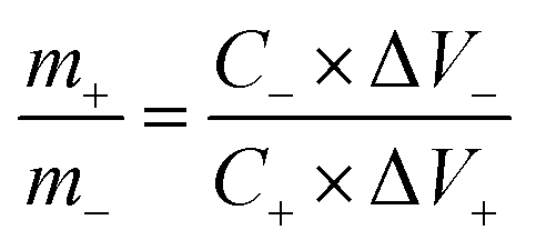 | (8) |
:2.18. Furthermore, the electrochemical properties of the individual A1 and graphite electrodes with a three electrode cell set up were studied via CV at 100 mV s−1, as shown in Fig. 6(a1).
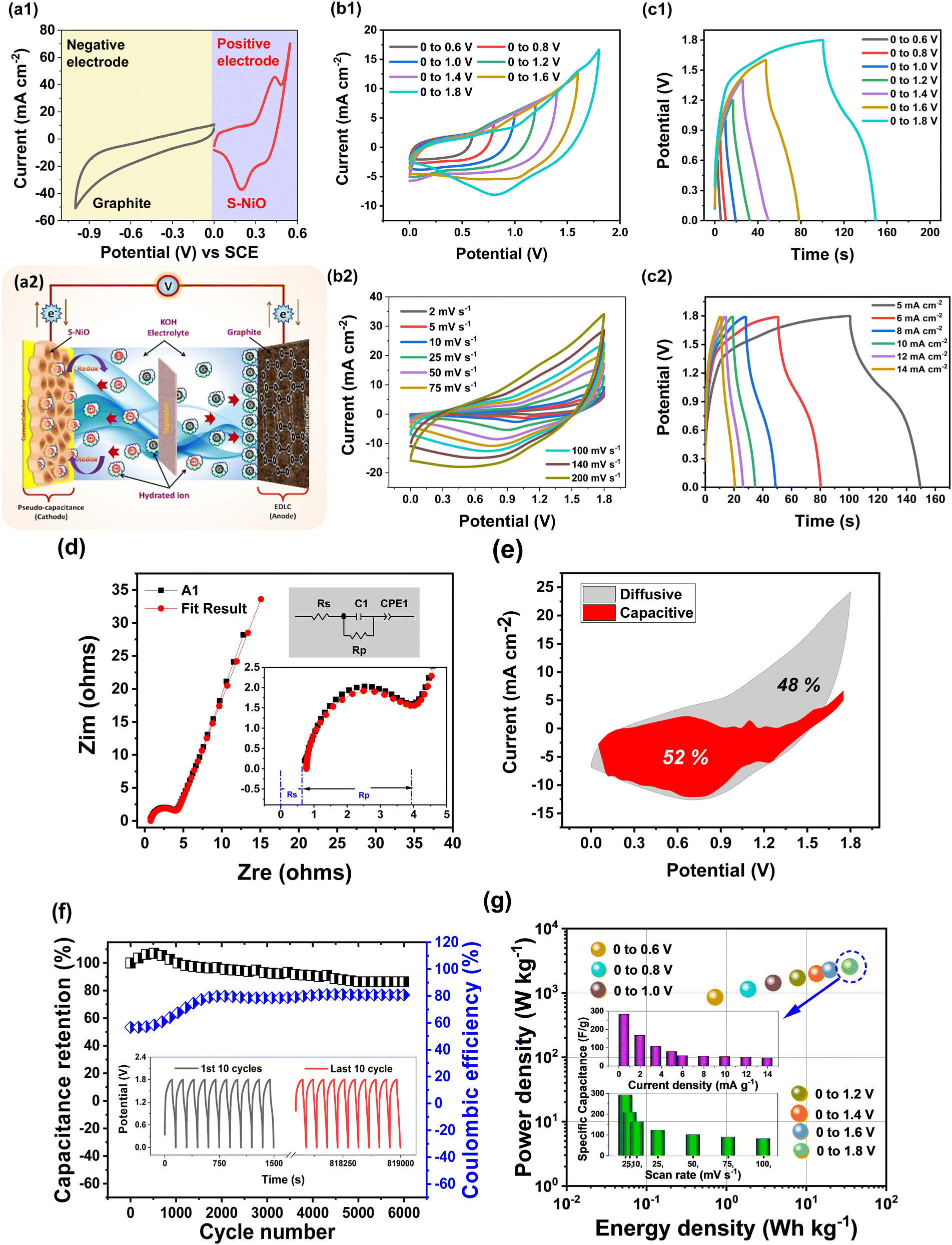 | ||
| Fig. 6 a1) CV testing of individual graphite and S-NiO (A1) electrodes, (a2) schematic of AAHSc (S-NiO//KOH//graphite) device, (b1) CVs of operating potential window variation from 0.6 to 1.8 V at 50 mV s−1, (b2) scan rate variation from 2 to 200 mV s−1, for optimized 1.8 V window, (c1) GCDs of operating potential window variation from 0.6 to 1.8 V at 5 mA cm−2, (c2) current density variation from 5 to 14 mA cm−2 for optimized 1.8 V window, (d) EIS (Nyquist) plot of device matched with fit result for suitable circuit. (e) Capacitive and diffusive current contribution at 100 mV s−1. (f) Cyclic stability and coulombic efficiency over 6000 cycles. (g) Ragone plot of device over various potential windows. The inset shows a bar diagram of the calculated specific capacitance using scan rate and current density. | ||
Herein, the A1 electrode is operated from 0 to 0.55 V, while the graphite electrode is operated from 0 to −1 V. Accordingly, AAHSc could afford to attain a high voltage window of 1.8 V due to the hybrid approach. The schematic illustration of the assembled A1//KOH//graphite (AAHSc) device is shown in Fig. 6(a2) and 6(b1) reveals CV plots measured for different potential windows (0 to 0.6 V to 0 to 1.8 V) at 50 mV s−1 scan rate. At voltage windows up to 0.8 V, the approximately rectangular CV shape corresponds to EDLC behaviour. Furthermore, the redox peak started to appear in the CV curves as the voltage window increased up to 1.2 V, reflecting pseudocapacitive characteristics due to the faradaic redox mechanism of the A1 electrode. As the potential window increased from 0.6 V to 1.8 V, the specific capacitance increased significantly at the 50 mV s−1 scan rate from 33.15 to 99.80 F g−1.
Fig. 6(b2) shows that the CV shape is well-maintained even at a high scan rate of 200 mV s−1, which suggests the fast current response activity of the electrodes. CV curves of an AAHSc device prominently depicted a large current response at a higher scan rate without oxygen and hydrogen evolution, which confirmed an efficient charge storage behaviour. The specific capacitance of an AAHSc device delivered 99.80 F g−1 at 50 mV s−1 and the value is retained up to 80.36 F g−1 at 100 mV s−1, indicating great capacitance rate performance. The specific capacitance values concerning the variation of the potential window, scan rate and current density are tabulated in Table ST4 (ESI†).
As shown in Fig. 6(c1), GCD curves of the AAHSc device were tested at various potential windows up to 1.8 V at a constant 5 mA cm−2 current density. As the potential window increases from 0.6 V to 1.8 V, the specific capacitance increases significantly from 14.40 to 77.69 F g−1, as obtained from equation 6. Fig. 6(c2) illustrates GCD tests conducted at various current densities ranging from 5 to 14 mA cm−2. The symmetrical charge and discharge curves deliver great capacitive performance. Based on GCD evaluation, the AAHSc device delivers a specific capacitance of 77.69 F g−1 at 5 mA cm−2 and maintains 43.03 F g−1 at 14 mA cm−2. This signifies excellent capacitance rate performance. The hybrid approach of the device achieves the operation at the higher potential window with a superior specific capacitance value.
Fig. 6(d) shows a Nyquist plot in the frequency range of 10 kHz to 0.01 Hz. The inset shows the equivalent circuit diagram to fit the results, and a magnified image at the lower frequency region. In the high frequency region, the intercept of the semicircles with the x-axis corresponds to the solution resistance (Rs) of electrolyte and the diameter of the semicircle corresponds to the polarisation resistance (Rp). The well fitted circuit revealed low values of Rs = 0.77 Ω and Rp = 3.11 Ω. The slope in the lower frequency region seems to be less, i.e. the diffusive resistance of the electrolyte in the AAHSc device seems to be smaller. Fig. 6(e) shows capacitive and diffusive current contributions of 52% and 48%, respectively, for the AAHSc device, at a higher scan rate of 100 mV s−1. These studies evidently suggested that a hybrid based combined charge storage mechanism, i.e. faradaic and non-faradaic current contribution, is reflected in the AAHSc device.
Fig. 6(f) reveals that the cyclic stability of the AAHSc device at 5 mA g−1 current density, for 6000 charging–discharging cycles, retained 91% of the initial capacitance. The coulombic efficiency was 80% after the 6000 cycles in aqueous 1 M KOH. The capacitance retention indicates a modest decline from 77.69 to 70.07 F g−1 after 6000 cycles, suggesting asymmetric hybrid supercapacitors deliver higher energy and power densities than EDLCs without sacrificing cycling rate capability.
Fig. 6(g) shows the correspondence between calculated energy densities (E) and power densities (P) of the AAHSc device with respect to potential window variation using eqn (9) and (10), respectively.73 The inset image in Fig. 6(g) shows a bar diagram of the calculated specific capacitance w.r.t. scan rates and energy densities.
 | (9) |
 | (10) |
| S. no. | Material | Electrolyte | Device capacitance | Energy density | Power density | Stability | Ref. |
|---|---|---|---|---|---|---|---|
| 1 | N-Doped carbon from NiO arrays|Ni foam | 2 M KOH | 88.8 F g−1 at 0.4 A g−1 | 27.75 W h kg−1 | 300 W kg−1 | 84.2% after 10000 cycles |
74 |
| 2 | Graphite-CNT @NiO//graphene-CNT | 2 M KOH | — | 11.9–23.4 W h kg−1 | 1060–7140 W kg−1 | 80% after 30000 cycles |
75 |
| 3 | NiO/C-HS//AC NiO-HS//AC | 2 M KOH | NiO/C-HS//AC = 99 F g−1, NiO-HS//AC = 32 F g−1, both at 0.25 A g−1 | NiO/C-HS//AC = 30.5 W h kg−1 NiO-HS//AC = 10.2 W h kg−1 | NiO/C-HS//AC = 193 W kg−1 NiO-HS//AC = 182 W kg−1 | 83% after 5000 cycles | 76 |
| 4 | NiO|copper sheets | 2 M KOH | — | 8.78 W h kg−1 | 2500 W kg−1 | 131% after 5000 cycles | 77 |
| 5 | Ni-NiO micro flower |carbon cloth | 1 M KOH | — | 15.9 W h kg−1 | 120 W kg−1 | 80% after 10000 cycles |
78 |
| 6 | Carboxyl groups (CPS) @ Ni |CPS core | 2 M KOH | — | 19.44 W h kg−1 | 2460 W kg | 100% after 1000 cycles | 79 |
| 7 | NiO/Ni3S2//AC | 3 M KOH | — | 52.9 W h kg−1 at 1600 W kg−1 | 26.3 W h kg−1 at 6400 W kg−1 | 92.9% over 5 000 cycles | 80 |
| 8 | NC/Ni@NiO//AC | 6 M KOH | 71.4 F g−1 at 1 A g−1 | 19.4 W h kg−1 | 700 W kg−1 | 73.8% after 3000 cycles | 81 |
| 9 | MnO2/NiO@Ni//rGO | 1 M KOH | 215 F g−1 | 59.5 W h kg−1 | 2530 W kg−1 | 75% after 10000 cycles | 82 |
| 10 | NiO/Ni(OH)2//AC | KOH/PVA | — | 28.5 W h kg−1, | 450 W kg−1 | 86.8% after 5000 cycles | 83 |
| 11 | NiMoO4/NiO//AC | 3 M KOH | — | 38 W h kg−1 | 96 W kg−1 | 95.5% after 5000 cycles | 84 |
| 12 | NiCo2O4/NiO/Co3O4//AC | 121 F g−1 at 1 A g−1 | 43.02 W h kg−1 | 820.29 W kg−1 | 83% after 2000 cycles | 85 | |
| 13 | NiO@NFC//NiO@NFC | Li-gel | 161 F g−1 at 1.0 A g−1 | 22 W h kg−1 | 491.9 W kg−1 | 96.0% after 5000 cycles | 86 |
| 14 | NiO@ITO//NiO@ITO | Li-gel | 85 F g−1 at 1.0 A g−1 | 11.8 W h kg−1 | 500 W kg−1 | 92.2% after 5000 cycles | 86 |
| 15 | ZnO/NiO//ZnO/NiO | — | 26.73 W h kg−1 | 641.5 W kg−1 | 73.43% after 5000 cycles | 87 | |
| 16 | PNFA//PNFA Porous NiO nanoflake array (PNFA) | 2 M KOH | — | 39.3 W h kg−1 | 550 W kg−1 | 92.4% after 5000 cycles | 88 |
| 17 | NiO//NiO | 6 M KOH | 307 F g−1 at 0.5 A g−1 | 10.53 W h kg−1 | 124.31 W kg−1 | 96% after 3000 cycles | 89 |
| 18 | NiO//α-Fe2O3 | PVA/KOH | — | 12.4 W h kg−1 | 951 W kg−1 | 85% after 10000 cycles | 90 |
| 19 | NiCo2O4/NiO//Fe2O3 | 1 M KOH | 79 F g−1 at 1 mA cm−2 | 19 W h kg−1 | 157 W kg−1 | 97% after 5000 cycles | 91 |
| 20 | S-NiO//graphite (AAHSc) | 1 M KOH | 77.69 F g−1 at 5 mA cm−2 | 34.96 W h kg−1 at 2567 W kg−1 | 19.36 W h kg−1 at 7180 W kg−1 | 91% after 6000 cycles | This work |
Fig. 7 shows a Ragone plot including a comparison with other reported work. Benefiting from the honeycomb like pseudo-based S-NiO electrode and EDLC based graphite as a negative electrode, AAHSc exhibits a higher energy density of 34.96 W h kg−1 at a power density of 2.5 kW kg−1 and remains at an energy density of 19.36 W h kg−1 at a power density of 7.18 kW kg−1. These values are comparable with or even higher than those from previously reported literature summarized in Table 1.74–91
 | ||
| Fig. 7 Ragone plot of the S-NiO//KOH//graphite AAHSc device (this work) with improved energy density values compared with other EDLC and pseudo based supercapacitor devices. | ||
It is observed that NiO based EDLC could achieve a high power density and NiO based pseudocapacitors could achieve a high energy density. Moreover, considerable improvement in energy density is achieved while retaining a high power density for the (S-NiO//KOH//graphite) AAHSc device. This work is placed at the top right corner of the Ragone plot as shown in Fig. 7. The detailed energy and power density values of the AAHSc device compared with those in EDLC and pseudocapacitor based reported literature are shown in Table 1. In summary, the cost-effective CDA mechanism reinforced a feasible approach of using S-NiO as a potential candidate owing to excellent electrochemical performance in an aqueous asymmetric hybrid supercapacitor device.
In summary, the chemically synthesized sulfur doped NiO electrodes produced via the CDA mechanism played a crucial role in growth as well as structural, morphological, and compositional aspects of the electrode materials, with superior impact on electrochemical performance and long-term stability. The crystallinity improvement was attributed to annealing, with surface morphology changes that are beneficial to the electrochemical performance of the sulfur doped NiO structure accompanied by the lowest dislocation density and microstrain. This facilitates favourable conditions for fast charge discharge progression pathways for the rapid transfer of electrons originating from sulfur doping. The Ni rich and high oxygen vacancies of the crystalline S-NiO served as active resources and resulted in improved electrical conductivity. Faradaic redox reactions involve adsorption–desorption of hydroxyl ions at the surface of the honeycomb like structured S-NiO. More active surface sites resulting in more electrolyte access with extra charge accumulation are made possible by cavities in the honeycomb-like structure. This satisfies key requirements for an effective supercapacitor electrode and supports improved electrochemical properties. Thus, the synergistic characteristics of the sulfur doped NiO structure facilitates the AAHSc device with ease, and is feasible for energy storage applications.
Conclusions
In conclusion, a sulfur doped nickel oxide material on a stainless-steel substrate is effectively prepared via a successful chemical bath method. The CDA mechanism assists the structural-morphological evolution and offers improved electrochemical functioning of the S-NiO electrode for the AAHSc device. The structural evolution of the S-NiO was observed from amorphous to crystalline, and was influenced by the CDA mechanism. Increasing the capping rate affected the elemental composition by decreasing the active Ni and S content in the sample. A cavity surface of an S-NiO honeycomb nanostructure exhibited notable specific capacitance values of 791.67 F g−1 and 766 F g−1 at a 20 mV s−1 scan rate and 0.8 mA cm−2 current density, respectively. The AAHSc fabricated by assembly with pseudocapacitive S-NiO as the positive electrode and EDLC-type graphite as the negative electrode synergistically achieved a higher cell voltage up to 1.8 V and a maximum specific capacitance of 77.69 F g−1 at 5 mA cm−2. Surface reactivity improvement was caused by morphology modification and rich Ni2+ sites along with sulfur doping, i.e. oxygen deficiency of the electrode. This would lead to fast and efficient charge storage to boost the supercapacitive performance of the S-NiO//KOH//graphite AAHSc device with a high energy density of 34.96 W h kg−1 and high power density of 7.18 kW kg−1. The high rate capability of 91% capacity retention results in 81% coulombic efficiency being sustained after 6,000 cycles. These results demonstrate an aqueous asymmetric hybrid approach toward cost effective and high-performance electrodes for energy storage applications.Conflicts of interest
The authors declare that they have no known competing financial interests or personal relationships that could have appeared to influence the work reported in this paper.Acknowledgements
One of the authors and P. I. of major research project Dr Sachin Babasaheb Kulkarni is thankful to Science and Engineering Research Board (SERB) New Delhi, Government of India for financial assistance through ECRA scheme file no. ECR/2017/002820.References
- S. Kiruthika, N. Sneha and R. Gupta, J. Mater. Chem. A, 2023, 11, 4907–4936, 10.1039/D2TA07836H.
- X. Ren, H. Wang, J. Chen, W. Xu, Q. He, H. Wang, F. Zhan, S. Chen and L. Chen, Small, 2023, 19, 2204121, DOI:10.1002/smll.202204121.
- J. Chen, W. Xu, H. Wang, X. Ren, F. Zhan, Q. He, H. Wang and L. Chen, J. Mater. Chem. A, 2022, 10, 21197–21250, 10.1039/D2TA05309H.
- F. Zhan, H. Wang, Q. He, W. Xu, J. Chen, X. Ren, H. Wang, S. Liu, M. Han, Y. Yamauchi and L. Chen, Chem. Sci., 2022, 13, 11981–12015, 10.1039/D2SC04012C.
- W. Zhou, K. Zhou, X. Liu, R. Hu and H. Liu, J. Mater. Chem. A, 2014, 2, 7250–7255, 10.1039/C3TA15280D.
- J. Bao, Z. Wang, W. Liu, L. Xu, F. Lei, J. Xie and Y. Zhao, J. Alloys Compd., 2018, 764, 565–573, DOI:10.1016/j.jallcom.2018.06.085.
- L. Liu and Z. Niu, Chin. Chem. Lett., 2018, 29, 571–581, DOI:10.1016/j.cclet.2018.01.013.
- S. R. KA and C. S. Rout, J. Mater. Chem. A, 2023, 11, 5495–5519, 10.1039/D2TA09824E.
- H. Wang, Q. He, F. Zhan and L. Chen, J. Colloid Interface Sci., 2023, 630, 286–296, DOI:10.1016/j.jcis.2022.09.092.
- Y. Li, B. Huang, X. Zhao, Z. Luo, S. Liang and H. Qin, J. Power Sources, 2022, 527, 231149, DOI:10.1016/j.jpowsour.2022.231149.
- Y. Li, Z. Luo, H. Qin, S. Liang, L. Chen and H. Wang, J. Colloid Interface Sci., 2021, 582, 842–851, DOI:10.1016/j.jcis.2020.08.097.
- H. Wang, Q. He, S. Liang, Y. Li, X. Zhao and L. Mao, Energy Storage Mater., 2021, 43, 531–578, DOI:10.1016/j.ensm.2021.09.023.
- D. P. Chatterjee and A. K. Nandi, J. Mater. Chem. A, 2021, 9, 15880–15918, 10.1039/D1TA02505H.
- L. Bai, H. Huang, S. Yu, D. Zhang and H. Huang, J. Energy Chem., 2022, 64, 214–235, DOI:10.1016/j.jechem.2021.04.057.
- M. Wu, X. Hu, W. Zheng, L. Chen and Q. Zhang, Chem. Eng. J., 2023, 466, 143077, DOI:10.1016/j.cej.2023.143077.
- Y. Ye, X. Guo, Y. Ma, Q. Zhao, Y. Sui, J. Song and W. Ma, J. Electroanal. Chem., 2021, 89, 7115588, DOI:10.1016/j.jelechem.2021.115588.
- R. Manikandan, C. J. Raj, G. Nagaraju and M. Pyo, J. Mater. Chem. A, 2019, 7, 25467–25480, 10.1039/C9TA08527K.
- S. B. Kulkarni, U. M. Patil, R. R. Salunkhe and S. S. Joshi, J. Alloys Compd., 2011, 509, 3486–3492, DOI:10.1016/j.jallcom.2010.12.036.
- U. M. Patil, S. B. Kulkarni and V. S. Jamadade, J. Alloys Compd., 2011, 509, 1677–1682, DOI:10.1016/j.jallcom.2010.09.133.
- J. Li, D. Xiong, L. Wang, M. K. S. Hirbod and X. Li, J. Energy Chem., 2018, 37, 66–72, DOI:10.1016/j.jechem.2018.11.015.
- B. Pandit, D. P. Dubal, P. Gómez-Romero and B. B. Kale, Sci. Rep., 2017, 7, 1–12, DOI:10.1038/srep43430.
- M. B. Poudel and H. J. Kim, J. Energy Chem., 2022, 64, 475–484, DOI:10.1016/j.jechem.2021.05.002.
- J. Li, S. Luo, B. Zhang, J. Lu, W. Liu, Q. Zeng and J. Wan, Nano Energy, 2020, 79, 2211–2855, DOI:10.1016/j.nanoen.2020.105410.
- J. Li, J. Zhao, L. Qin, Q. Zhang, X. Tang and Y. Xu, RSC Adv., 2020, 10, 22606–22615, 10.1039/d0ra03253k.
- L. Yang, M. Huang, M. Lu, X. Guan and X. Guan, J. Chem. Eng., 2019, 364, 462–474, DOI:10.1016/j.cej.2019.01.107.
- Z. Wu, X. L. Huang, Z. L. Wang, J. J. Xu and H. G. Wang, Sci. Rep., 2014, 4, 2045–2322, DOI:10.1038/srep03669.
- H. Wang, X. Ren, J. Chen, W. Xu, Q. He and H. Wang, J. Power Sources, 2023, 554, 232309, DOI:10.1016/j.jpowsour.2022.232309.
- H. Heydari, S. E. Moosavifard and M. Shahraki, J. Energy Chem., 2017, 26, 62–767, DOI:10.1016/j.jechem.2017.03.007.
- M. Acerce, D. Voiry and M. Chhowalla, Nat. Nanotechnol., 2015, 10, 313–318, DOI:10.1038/nnano.2015.40.
- A. M. Patil, A. C. Lokhande, P. A. Shinde and J. H. Kim, J. Energy Chem., 2018, 27, 791–800, DOI:10.1016/j.jechem.2017.05.005.
- F. Liu, X. Wang, J. Hao, S. Han, J. Lian and Q. Jiang, Sci. Rep., 2017, 7, 2045–2322, DOI:10.1038/s41598-017-17899-6.
- J. W. Lee, T. Ahn, J. H. Kim, J. M. Ko and J. D. Kim, Electrochim. Acta, 2011, 56, 4849–4857, DOI:10.1016/j.electacta.2011.02.116.
- W. Yu, X. Jiang, S. Ding and B. Q. Li, J. Power Sources, 2014, 256, 440–448, DOI:10.1016/j.jpowsour.2013.12.110.
- C. Yuan, X. Zhang, L. Su, B. Gao and L. Shen, J. Mater. Chem., 2009, 19, 5772–5777, 10.1039/B902221J.
- A. Paravannoor, R. Ranjusha, A. M. Asha and R. Vani, J. Chem. Eng., 2013, 220, 360–366, DOI:10.1016/j.cej.2013.01.063.
- K. Karuppasamy, D. Vikraman, J. H. Jeon and S. Ramesh, Appl. Surf. Sci., 2020, 529, 147147, DOI:10.1016/j.apsusc.2020.147147.
- W. Xu, X. Zhao, F. Zhan, Q. He, H. Wang and J. Chen, Energy Storage Mater., 2022, 53, 79–135, DOI:10.1016/j.ensm.2022.08.039.
- S. Li, Y. Ruan and Q. Xie, Electrochim. Acta, 2020, 356, 136837, DOI:10.1016/j.electacta.2020.136837.
- Z. Huang, X. Li, X. Xiang, T. Gao and Y. Zhang, J. Mater. Chem. A, 2018, 6, 23746–23756, 10.1039/C8TA08897G.
- V. T. Chebrolu, B. Balakrishnan, I. Cho, J. S. Bak and H. J. Kim, Dalton Trans., 2020, 49, 14432–14444, 10.1039/D0DT00263A.
- X. Yan, X. Tong, J. Wang, C. Gong and M. Zhang, J. Alloys Compd., 2014, 593, 184–189, DOI:10.1016/j.jallcom.2014.01.036.
- M. S. Wu, Y. P. Lin, C. H. Lin and J. T. Lee, J. Mater. Chem., 2012, 22, 2442–2448, 10.1039/C1JM13818A.
- B. Zhao, J. Song, P. Liu, W. Xu, T. Fang and Z. Jiao, J. Mater. Chem., 2011, 21, 18792–18798, 10.1039/C1JM13016A.
- W. Ji, J. Ji, X. Cui, J. Chen, D. Liu and H. Deng, Chem. Commun., 2015, 51, 7669–7672, 10.1039/C5CC00965K.
- G. H. Guai, M. Y. Leiw, C. M. Ng and C. M. Li, Adv. Energy Mater., 2012, 2, 334–338, DOI:10.1002/aenm.201100582.
- B. S. Singu, S. E. Hong and K. R. Yoon, J. Ind. Eng. Chem., 2018, 62, 321–328, DOI:10.1016/j.jiec.2018.01.010.
- J. Chang, K. Li, Z. Wu, J. Ge and C. Liu, ACS Appl. Mater. Interfaces, 2018, 10, 26303–26311, DOI:10.1021/acsami.8b08068.
- T. Li, J. Yin, Y. Li, Z. Tian, Y. Zhang, L. Xu and Y. Li, J. Energy Chem., 2021, 63, 585–593, DOI:10.1016/j.jechem.2021.08.035.
- P. Yang, L. Li, S. Yu, H. Zheng and W. Peng, Appl. Surf. Sci., 2019, 1, 396–403, DOI:10.1016/j.apsusc.2019.06.223.
- A. Diallo, K. Kaviyarasu and S. Ndiaye, Green Chem. Lett. Rev., 2018, 11, 166–175, DOI:10.1080/17518253.2018.1447604.
- Z. W. Wang, Y. B. Wang, X. Z. Liao, Y. H. Zhao and E. J. Lavernia, Scr. Mater., 2009, 60, 52–55, DOI:10.1016/j.scriptamat.2008.08.032.
- J. Madhavi, SN Appl. Sci., 2019, 1, 1509, DOI:10.1007/s42452-019-1291-9.
- X. A. Zhu and C. T. Tsai, J. Appl. Phys., 2005, 97, 043520, DOI:10.1063/1.1848190.
- M. Babikier, D. Wang, J. Wang, Q. Li, J. Sun and Y. Yan, J. Mater. Sci.: Mater. Electron., 2013, 25, 157–162, DOI:10.1007/s10854-013-1566-7.
- K. Zhou, Z. Qi, B. Zhao, S. Lu, H. Wang, J. Liu and H. Yan, Surf. Interfaces, 2017, 6, 91–97, DOI:10.1016/j.surfin.2016.12.004.
- K. K. Purushothaman and G. Muralidharan, Sol. Energy Mater. Sol. Cells, 2009, 93, 1195–1201, DOI:10.1016/j.solmat.2008.12.029.
- R. Sharma, A. D. Acharya, S. B. Shrivastava and T. Shripathi, Optik, 2014, 125, 6751–6756, DOI:10.1016/j.ijleo.2014.07.104.
- U. M. Patil, R. R. Salunkhe and K. V. Gurav, Appl. Surf. Sci., 2008, 255, 2603–2607, DOI:10.1016/j.apsusc.2008.07.192.
- X. Y. Deng and Z. Chen, Mater. Lett., 2004, 58, 276–280, DOI:10.1016/S0167-577X(03)00469-5.
- X. Chen, N. Zhang and K. Sun, Electrochem. Commun., 2012, 20, 137–140, DOI:10.1016/j.elecom.2012.04.009.
- J. Moghaddam and E. Hashemi, Korean J. Chem. Eng., 2014, 31, 503–508, DOI:10.1007/s11814-013-0233-2.
- C. Coudun, E. Amblard, J. Guihaumé and J. F. Hochepied, Catal. Today, 2007, 124, 49–54, DOI:10.1016/j.cattod.2007.01.064.
- A. Dutta and J. Datta, J. Mater. Chem. A, 2014, 2, 3237–3250, 10.1039/C3TA12708G.
- G. Wang, Z. Yan, N. Wang and M. Xiang, ACS Appl. Nano Mater., 2021, 4, 9034–9043, DOI:10.1021/acsanm.1c01628.
- A. Munir, T. Haq, A. Qurashi and H. U. Rehman, ACS Appl. Energy Mater., 2019, 2, 363–371, DOI:10.1021/acsaem.8b01375.
- Y. Wang, A. Pan, Y. Zhang, J. Shi and J. Lin, J. Mater. Chem. A, 2018, 6, 9153–9160, 10.1039/C8TA01866A.
- X. Ren, C. Guo, L. Xu, T. Li and L. Hou, ACS Appl. Mater. Interfaces, 2015, 7, 19930–19940, DOI:10.1021/acsami.5b04094.
- M. Huang, F. Li, J. Y. Ji, Y. X. Zhang, X. L. Zhao and X. Gao, CrystEngComm, 2014, 16, 2878–2884, 10.1039/C3CE42335B.
- J. Wang, J. Polleux, J. Lim and B. Dunn, J. Phys. Chem. C, 2007, 111, 14925–14931, DOI:10.1021/jp074464w.
- S. P. Gupta, M. A. More, D. J. Late and P. S. Walke, Electrochim. Acta, 2020, 366, 137389, DOI:10.1016/j.electacta.2020.137389.
- S. J. Marje, P. K. Katkar, S. S. Pujari and S. A. Khalate, Synth. Met., 2020, 259, 116224, DOI:10.1016/j.synthmet.2019.116224.
- H. S. Kim, J. B. Cook, H. Lin, J. S. Ko, S. H. Tolbert and V. Ozolins, Nat. Mater., 2016, 16, 454–460, DOI:10.1038/nmat4810.
- Z. Zhang, X. Huang, H. Li, H. Wang and Y. Zhao, J. Energy Chem., 2017, 26, 1260–1266, DOI:10.1016/j.jechem.2017.09.025.
- G. Qu, S. Jia, H. Wang, F. Cao, L. Li and C. Qing, ACS Appl. Mater. Interfaces, 2016, 8, 20822–20830, DOI:10.1021/acsami.6b06630.
- C. Guan, Y. Wang, Y. Hu, J. Liu, K. H. Ho and W. Zhao, J. Mater. Chem. A, 2015, 3, 23283–23288, 10.1039/C5TA06658A.
- T. Liu, L. Zhang, B. Cheng, W. You and J. Yu, Chem. Commun., 2018, 54, 3731–3734, 10.1039/C8CC00991K.
- V. Kannan, A. I. Inamdar, S. M. Pawar and H. S. Kim, ACS Appl. Mater. Interfaces, 2016, 8, 17220–17225, DOI:10.1021/acsami.6b03714.
- S. Ci, Z. Wen, Y. Qian, S. Mao and S. Cui, Sci. Rep., 2015, 5, 11919, DOI:10.1038/srep11919.
- L. Wang, H. Tian, D. Wang, X. Qin and G. Shao, Electrochim. Acta, 2015, 151, 407–414, DOI:10.1016/j.electacta.2014.11.050.
- S. Liu, S. C. Lee, U. M. Patil, C. Ray and K. V. Sankar, J. Mater. Chem. A, 2017, 5, 4543–4549, 10.1039/C6TA11049E.
- Y. Li, Q. Wei, R. Wang, J. Zhao, Z. Quan and T. Zhan, J. Colloid Interface Sci., 2020, 570, 286–299, DOI:10.1016/j.jcis.2020.03.004.
- S. Saha, S. Chhetri, P. Khanra, P. Samanta and H. Koo, J. Energy Storage., 2016, 6, 22–31, DOI:10.1016/j.est.2016.02.007.
- X. Chen, S. Wang, G. Qiao, G. Lu, H. Cui and X. Wang, Energy Fuels, 2020, 34, 16783–16790, DOI:10.1021/acs.energyfuels.0c02767.
- R. Xu, J. Lin, J. Wu, M. Huang, L. Fan, Z. Xu and Z. Song, Appl. Surf. Sci., 2019, 463, 721–731, DOI:10.1016/j.apsusc.2018.08.172.
- X. Feng, Y. Huang, C. Li, X. Chen, S. Zhou and X. Gao, J. Chem. Eng., 2019, 368, 51–60, DOI:10.1016/j.cej.2019.02.191.
- C. S. Kwak, T. H. Ko, J. H. Lee and H. Y. Kim, ACS Appl. Energy Mater., 2020, 3, 2394–2403, DOI:10.1021/acsaem.9b02073.
- Y. S. Nagaraju, H. Ganesh, S. Veeresh and H. Vijeth, Mater. Sci. Semicond. Process., 2022, 142, 106429, DOI:10.1016/j.mssp.2021.106429.
- J. Wang, F. Zheng, M. Li, D. Jia, X. Mao, J. Fu and P. Hu, J. Alloys Compd., 2022, 913, 165280, DOI:10.1016/j.jallcom.2022.165280.
- S. Goel, A. K. Tomar and R. K. Sharma, ACS Appl. Energy Mater., 2018, 1, 1540–1548, DOI:10.1021/acsaem.7b00343.
- S. Zhang, B. Yin, Z. Wang and F. Peter, J. Chem. Eng., 2016, 306, 193–203, DOI:10.1016/j.cej.2016.07.057.
- A. Shanmugavani and R. K. Selvan, Electrochim. Acta, 2016, 189, 283–294, DOI:10.1016/j.electacta.2015.12.043.
Footnotes |
| † Electronic supplementary information (ESI) available. See DOI: https://doi.org/10.1039/d3ma00373f |
| ‡ Equally contributed authors |
| This journal is © The Royal Society of Chemistry 2023 |