
 Open Access Article
 This Open Access Article is licensed under a Creative Commons Attribution-Non Commercial 3.0 Unported Licence
Crystal phase control in self-catalyzed GaAs nanowires grown on pre-etched Si substrates
Shan
Wang
abc,
Haolin
Li
ab,
Jilong
Tang
 ac,
Yubin
Kang
d,
Xiaohua
Wang
*ac,
Rui
Chen
*b and
Zhipeng
Wei
*a
ac,
Yubin
Kang
d,
Xiaohua
Wang
*ac,
Rui
Chen
*b and
Zhipeng
Wei
*a
aState Key Laboratory of High Power Semiconductor Laser, School of physics, Changchun University of Science and Technology, Changchun 130022, P. R. China. E-mail: biewang2001@126.com; zpweicust@126.com
bDepartment of Electrical and Electronic Engineering, Southern University of Science and Technology, Shenzhen, Guangdong, 518055, P. R. China. E-mail: chenr@sustech.edu.cn
cSemiconductor Laser and Application Laboratory, Zhongshan Institute of Changchun University of Science and Technology, Zhongshan, 528437, P. R. China
dCollege of Optics and Electronic Science and Technology, China Jiliang University, Hangzhou, 310018, P. R. China
First published on 6th September 2023
Abstract
Semiconductor nanowires play a very important role in optoelectronic devices due to their excellent photoelectric properties. However, the intermixing of zinc blende and wurtzite crystal phases limits the development of GaAs nanowires, and how to obtain pure phase GaAs nanowires has become a research hotspot. In this study, the Si substrate is pre-etched and pure ZB phase GaAs nanowires are obtained by changing the effective V/III flux ratio through the shadowing effect. A series of nanowires with different morphologies and optical properties were obtained by pre-etching the oxide layer on the Si substrate at different times. We observed that pure ZB phase GaAs nanowires with good verticality were obtained when the etching time was 3 s. The principles of crystal phase control and materials properties were discussed in detail. These results suggest that the growth method of pure phase nanowires reported herein can be applied to other low-dimensional materials, which could pave the way for future nanowire devices.
Introduction
Semiconductor nanowires have been considered to be the key components for future devices and systems due to their quantum confinement effect, large surface-to-volume ratio, and large absorption cross-section. Significant progress in nanowire-based devices such as solar cells,1,2 lasers,3–5 photodetectors,6 integrated photonic circuits, etc.7,8 has been achieved in the past few decades. In particular, GaAs nanowires, which are representative of III–V semiconductor materials, have shown great applications in the fields of communication and near-infrared detection.6,9–11 However, unlike their bulk counterparts which exhibit only stable zinc blende (ZB) phases, metastable wurtzite (WZ) phases often appear in low-dimensional III-V materials.12 In GaAs nanowires, the intermixing of ZB and WZ phases easily leads to structural defects that alter the band structure and reduce the mobility of charge carriers.13 Therefore, such crystal phase intermixing in GaAs nanowires affects their optoelectronic properties, resulting in low emission efficiency and optical gain. To improve the crystal quality of GaAs nanowires, much effort has been devoted to the growth of materials by metal–organic chemical vapor deposition (MOCVD) and molecular beam epitaxy (MBE) by optimizing the growth temperature, V/III flux ratio and catalyst.14–20 Although the ZB and WZ phases in nanowires could be controlled by precisely tuning the growth parameters, the realization of pure phase GaAs nanowires by simple methods has always been a hot topic.GaAs nanowires are usually grown based on the vapor–liquid–solid (VLS) mechanism, and using Au-catalytic or self-catalytic methods. The Au-catalytic method utilizes Au droplets as the catalyst, while the self-catalytic method uses a group III element, such as Ga for GaAs nanowires, as the catalyst.21 In comparison, the self-catalytic method is more widely used for growing nanowires due to the better growth quality, cleaner vacuum chamber and friendliness of Si-based integration. However, the growth of pure phase GaAs nanowires by the self-catalytic method is more challenging. With the development of research in this field, a nucleation-based model has been proposed to describe the surface energy and the formation energy. In this model, nucleation at the triple phase line (TPL) is typically used to solve the problem of WZ phase formation.12 The results show that the higher cohesive energy of the WZ phase can be compensated by the lower surface energy when nucleation occurs at the TPL. Since then, the nucleation theory of nanowire growth has been further developed to include additional effects such as particle surface area,22 Kashchiev renormalization,23 polynucleate,24 droplet morphology19,21 and droplet depletion.25
A recent study by Spirkoska et al.13 showed that increasing the V/III flux ratio while holding other parameters constant results in an increase in the fraction of the ZB structure. This is in contrast to previous predictions using the highly approximate classical two-dimensional (2D) nucleation theory,12,22,26 which has been used to describe the phase transition at the growth interface for Au-assisted NWs. Spirkoska et al.13 argued that a possible reason for their findings could be that the vapor pressure has a large effect on the effective edge energies of the 2D nucleus, which could affect the WZ and ZB nucleation rates and therefore possibly favor ZB at large V/III flux ratio. They also pointed out the possibility of a relatively larger area for ZB nucleation events than WZ due to the critical nuclei becoming smaller with increasing supersaturation, since ZB is favored for nucleation away from the triple phase line (TPL) and WZ at the TPL.
In the MBE growth of self-catalytic GaAs nanowires on a Si substrate, most studies have focused on growth conditions (V/III flux ratio, temperature, and Ga droplet pre-deposition), mainly to increase the nanowire growth yield.27–29 However, several important features in the manipulation of substrate design have received little attention. In particular, the influence of substrate etching on the growth kinetics, the crystal phase, and ultimately the resulting nanowire properties has been underexplored. Although there are reports of self-catalyzed growth of GaAs nanowires on Si substrates,17,30,31 the growth mechanism of pure phase nanowires is not clear. In the research on patterned substrates, the main purpose is to control the position of the nanowires.32,33
In this work, it is shown that crystal phase control for GaAs nanowires can be achieved based on a simple but effective substrate pre-etching process. Our use of only the Si native oxide as a masking layer for MBE growth is simpler for GaAs. A previous study has proposed the growth of In(As)P nanowires by in situ deposition of In droplets on silicon substrates with natural oxides by metal–organic vapor phase epitaxy without a catalyst.34 However, a considerable part of the nanowires are curved and of different lengths, and no completely vertical nanowires can be observed. According to the VLS growth mechanism of this work, we have obtained GaAs nanowires with high optical quality and good verticality. The density and size of the etched pinholes on the substrate determine the catalyst density, which in turn affects the equivalent V/III flux ratio during growth, and further affects the crystal phase of GaAs nanowires. Morphological and optical characterization was performed and the mechanism of crystal phase control was discussed in detail. These results suggest that the growth method proposed here can be applied to the growth of other semiconductor nanowires, which will be beneficial for research and application of nanoscale devices.
Experimental
Prior to the growth of nanowires, the Si substrate was pre-etched. Si(111) substrates were immersed into a 10% hydrofluoric acid (HF) solution. After this etching process, modification of the native oxide layer on the Si(111) substrate will result in pores with different densities for Ga droplets.16 Then, according to the self-catalytic methods, GaAs nanowires were grown on the pre-etched substrate using an MBE system (DCA P600). The growth temperature was maintained at 620 °C, and the V/III flux ratio was fixed at 26 (the As4 beam equivalent pressure was around 1.6 × 10⁻⁶ torr and the Ga beam flow rate was 6.2 × 10⁻⁸ torr). The total growth time was 30 min. Immediately after the growth was completed, the Ga shutter was closed while the As4 beam was maintained until the temperature cooled down to 400 °C.The morphological properties of the samples were analyzed using a Hitachi S-4800 field emission scanning electron microscope (SEM). Transmission electron microscopy (TEM) measurements were performed using a FEI Tecnai G2 F20 microscope operated at 200 kV. X-ray diffraction (XRD) measurements were carried out using a diffractometer (model ULTIMA IV, Rigaku, Japan) with a 2θ range of 25–30° using Cu Kα radiation (λ = 1.5418 Å) operating at 40 kV and 20 mA to determine the crystal phase of the samples. To discuss the optical properties of the samples, a 655 nm semiconductor diode laser was used as the excitation source. The emission from the samples was collected and dispersed using a HORIBA iHR550, and an InGaAs detector was used to detect the signal. A laser with an excitation power of 90 mW and a spot size of about 0.4 cm2 was used for the temperature-dependent photoluminescence (PL) measurements, while the temperature was fixed at 10 K for the power-dependent PL measurements. Confocal μ-Raman spectra were recorded using a WITec Alpha 300R Raman spectroscope (WITec, Ulm, Germany) equipped with a 532 nm laser. The laser excitation power was adjusted to approximately 3 mW.
Results and discussion
We fabricated a series of samples with different substrate etching times. GaAs nanowires were simultaneously grown on the Si wafers covered with silicon dioxide. The morphology of the as-grown GaAs nanowires was characterized and their optical images are shown in Fig. 1(a). Regions A, B, C and D correspond to the GaAs nanowires grown on the substrates with etching times of 0, 3, 6 and 9 s, respectively. The boundaries of different regions can be clearly seen, and the samples with different etching times show different colors under light illumination, which is due to the differences in nanowire density, diameter and orientation. From the following measurements, it is known that nanowire arrays with high density, large diameter and good verticality appear white in the optical image. We have measured different positions and found that the nanowires in the same region have similar properties. | ||
| Fig. 1 (a) Optical image of GaAs nanowires grown on different regions (half of a 2-inch Si wafer) classified by etching time. Regions A, B, C and D correspond to the GaAs nanowires grown on the substrates with etching times of 0, 3, 6 and 9 s, respectively. The V/III flux ratio of the samples is all fixed at 26. (b)–(e) SEM images of region A–D. (f) Diameter and density statistics of GaAs nanowires grown on the different regions. | ||
Fig. 1(b)–(e) show the top and cross-sectional SEM images of regions A, B, C and D shown in Fig. 1(a). In order to observe the overall verticality and growth density of the nanowires, we did not enlarge them with higher magnification. It can be seen intuitively that the perpendicularity of the nanowires in region A is poor. However, the nanowire perpendicularity in regions B and C has been improved, while the nanowire arrays in region B grow almost vertically. These phenomena are consistent with the previous research result, which proposed that for thicker oxides, the orientation of nanowires with respect to the substrate is random.35 In contrast, in region D, the perpendicularity of the nanowires is found to be worse again. The reasons for this phenomenon will be explained later. According to the literature,36 for Si(111) substrates, nanowires grown along the [0![[1 with combining macron]](https://www.rsc.org/images/entities/char_0031_0304.gif) 1] direction are considered as vertical ones. The yields of vertical GaAs nanowires in four regions have been calculated, and the values were 25%, 95%, 89% and 60%, respectively. These results show that the orientation of the nanowires is improved after the substrate is etched. To describe the morphology of the nanowires more intuitively, the diameter and density of the nanowires in different regions were counted, and the statistical results are plotted in Fig. 1(f). During the etching time from 0 to 6 s, the density of the nanowires shows an increasing trend, while the diameter of the nanowires gradually decreases. When the etching time is 6 s, the density and diameter reach their maximum and minimum values, respectively. When the etching time is further increased to 9 s, the density and diameter of the nanowires no longer follow the above trend, but show the opposite trend.
1] direction are considered as vertical ones. The yields of vertical GaAs nanowires in four regions have been calculated, and the values were 25%, 95%, 89% and 60%, respectively. These results show that the orientation of the nanowires is improved after the substrate is etched. To describe the morphology of the nanowires more intuitively, the diameter and density of the nanowires in different regions were counted, and the statistical results are plotted in Fig. 1(f). During the etching time from 0 to 6 s, the density of the nanowires shows an increasing trend, while the diameter of the nanowires gradually decreases. When the etching time is 6 s, the density and diameter reach their maximum and minimum values, respectively. When the etching time is further increased to 9 s, the density and diameter of the nanowires no longer follow the above trend, but show the opposite trend.
To explain the different orientations of the GaAs nanowires grown on substrates with different etching times as shown in Fig. 1, the evolution of the substrate with different etching times is shown in Fig. 2(a). During the self-catalytic growth, we have found that the interaction of the reactive gallium with the SiO2 pinholes induces the formation of nanocraters, which is an important prerequisite for the nucleation of the nanowires.37,38 Ga droplets are formed inside the etched pinholes, and the growth direction of the nanowires is related to the contact angle between the catalysts and the substrate.19 The natural oxide layer on top of the Si substrate has poor uniformity.38 Previous scanning tunneling microscopy studies confirm that Ga atoms tend to accumulate in existing defects on SiO2 surfaces, leading to the formation of larger nanocavities.39 When Ga droplets are deposited directly on the untreated Si substrate, the larger and sparser holes on the surface of the oxide layer become the attachment points for the Ga droplets. The droplet will not completely fill these holes resulting in a contact angle between the droplet and the substrate of less than 90°. In this case, the nanowires tend to grow parallel to the substrate after nucleation at the TPL.19,40 Therefore, the nanowires grown in region A have poor perpendicularity, large diameter and low density. When the substrate is etched for 3 and 6 s, HF removes some of the natural oxide layer, which changes the size and density of the original holes. The holes created by the etched substrate are called pinholes. Previous studies have shown that gallium atoms interact with SiO2 to form sparse nanocraters on pre-existing subnanometer pinholes. As the oxide layer on the surface of the substrate thins, the nanocraters reach the underlying Si surface and form an epitaxial relationship with the GaAs nanowires. Similar to the situation reported in the literature, when nanowires grow in contact with the substrate, they tend to grow vertically in Si(111).38,41,42 In addition, the contact angle between the droplet and the substrate decreases with decreasing pinhole size, and the nanowires prefer to grow more vertically. This is consistent with the results observed in Fig. 1. When the etching time is 9 s, the natural oxide layer on the substrate is almost etched away. At this point, the natural oxide layer is so thin that some of the etched pinholes disappear. Under the same growth conditions, a shallower depth will cause the droplet to overflow from the etched pinhole and merge with the surrounding ones, increasing the size and the contact angle between the droplet and the substrate. In this case, the shape of the droplet will be asymmetric, and the nanowires may grow outside the etched pinhole. Vertical growth of the nanowires is then not guaranteed due to the poor confinement. A. Fontcuberta i Morral et al.38 concluded that growth directly on a GaAs surface under the same conditions did not result in the formation of nanowires. Mattila et al.34 also came to a similar conclusion. In our study, the silicon dioxide layer in region D has been partially removed, which may reduce the growth of nanowires and lead to a decrease in nanowire density.
 | ||
| Fig. 2 (a) Schematic diagrams of the substrates etched for 0, 3, 6, and 9 s, respectively. (b) Schematic diagram of single GaAs nanowire growth. (c) and (d) Schematic diagrams of the self-catalytic growth of GaAs nanowires without and with shadowing effect, respectively. Light green areas indicate that there is no competition among adatoms, while dark green areas indicate that there is competition among them. | ||
The size and density of the etched pinholes will also affect the effective V/III flux ratio during the growth due to the shadowing effect.43–45 To explain the growth mechanism, schematic diagrams have been drawn and are shown in Fig. 2(b)–(d). At the very beginning of the nanowire growth, the catalyst is formed inside the etching pinhole. Once the droplet is oversaturated with the group V flux, the nanowire starts to grow along the axis. At the same time, the group III flux should be maintained to prevent the droplet from being consumed. During the growth of the GaAs nanowires, there are three different sources of elements,44,46 namely, the direct impingement on the droplet surface, adsorption on the substrate surface and the nanowire sidewalls. Fig. 2(b) illustrates the growth of a single GaAs nanowire based on the model of Peter Krogstrup.17 The adsorbed atoms would diffuse into the droplet along the substrate surface and the nanowires' sidewalls. There are two distinct growth regimes in the nanowire growth, i.e., a diffusion-limited and competitive regime, as previously reported for NW growth in other III–V material systems.47,48 For the adsorption of atoms from the substrate, the average migration distance prior to incorporation is defined as the diffusion length, and denoted by R. The circular area formed with a radius of R is called the diffusion area. When multiple catalysts are formed simultaneously, as long as their diffusion areas do not overlap, that is, the diffusion length is shorter than the distance between adjacent etched pinholes, the effective diffusion area will still be determined by the diffusion length, as shown in Fig. 2(c). The Ga flux is limited by substrate surface diffusion alone, which is called the diffusion-limited growth regime. In this regime, the supplied Ga outside the diffusion region of the nanowires hits the SiO2/Si(111) substrate too far away from the NW, and thus, cannot be collected in the NW but rather desorbs or nucleates in the form of parasitic GaAs clusters.43 Since the catalyst droplets formed are dense on the substrate, the collection of Ga adatoms is obviously strongly governed by the distance between adjacent NWs, as shown in Fig. 2(d). In this competitive regime, Ga adatom flux to the NW growth front is limited by two mechanisms: In the early growth stage, when growth is mainly controlled by surface diffusion on the SiO2 mask, Ga collection is limited by material competition. With increasing growth time also the collection of adatoms impinging on the GaAs NW sidewalls also becomes important. Here, the arrival rate of directly impinging Ga adatoms and the subsequent sidewall diffusion to the Ga droplet becomes increasingly shadowed by the high density of neighboring NWs. Thus, a reduction in the effective Ga flux at the growth front is expected.43 It is important to note that the distance between nanowires primarily affects the local Ga flux, and hardly affects the As flux. Arsenic contributes to NW growth mainly by direct impingement on the Ga droplet and not via surface diffusion.35,49 This effect, hereafter referred to as the shadowing effect, will limit the Ga flux into the Ga droplets and increase the V/III flux ratio. According to the previous introduction, this will be more favorable for the growth of pure-phase GaAs nanowires.
In order to intuitively characterize the crystal phase in the GaAs nanowires grown on the substrate with different etching times, TEM characterization of the GaAs nanowires in regions A and B was performed and the results are shown in Fig. 3. Fig. 3(a) shows the TEM image of GaAs nanowires grown in region A. In the magnified TEM as shown in the inset of Fig. 3(a), the yellow circles mark the ZB phases and the white triangles mark the WZ phases. It can be seen that there is severe phase intermixing formed as stacking faults along the nanowires. This observation is also supported by the diffraction pattern of the nanowires in region A shown in Fig. 3(b). Fig. 3(c) shows the GaAs nanowires grown in region B. The inset shows the TEM magnification of a small section of the GaAs nanowire. It can be seen that the diameter of the nanowires is reduced and no distinct phase intermixing can be observed. The diffraction pattern in Fig. 3(d) also suggests that the crystal phase of the GaAs nanowires is pure ZB.
 | ||
| Fig. 3 (a) TEM image of GaAs nanowires grown in region A. The filled yellow circles mark the ZB phase while filled white triangles indicate the WZ phase in the inset. (b) Diffraction pattern of GaAs nanowires grown in region A. (c) TEM image of the GaAs nanowires grown in region B. (d) Diffraction pattern of GaAs nanowires grown in region B. | ||
Based on different as-grown nanowires with variable substrate etching time, we clearly show the existence of different crystal phases, which strongly depend on the size and density of etched pinholes and which further lead to distinct differences in the physical properties, such as the PL characteristics. To further verify the regular changes in the energy band structure and carrier distribution of nanowires grown in different regions, the optical properties of the entire array were characterized. Fig. 4(a) shows the low temperature (10 K) PL from GaAs nanowires grown in different regions. Before performing PL experiments on the samples, we used the mechanical method to transfer nanowires out of the substrate and performed luminescence experiments on the substrate parasites. The experimental results excluded the possibility of PL from these parasites and ensured that the PL experiment data were derived from nanowires. It can be seen that all samples exhibited the GaAs excitonic emission at 1.515 eV due to the presence of ZB crystal phases.13 For easier comparison, all spectra have been normalized to this peak. It can be seen that all samples have another emission with a photon energy of 1.492 eV. Considering the metastable WZ crystal phase, the emission at 1.492 eV is then considered to be related to the coexistence of the WZ and ZB phases in the GaAs nanowires.50 The band gap of the WZ and ZB phases in GaAs nanowires is different. The conduction band and the valence band of the WZ crystal phase of GaAs are higher than those of ZB. Therefore, a type II band structure will be formed at the interface. In this structure, electrons are confined in the conduction band of the ZB phases, and holes are confined in the valence band of the WZ phases. Therefore, electrons and holes recombine and give rise to emission with a photon energy of 1.492 eV.13 It is interesting to note that this peak exhibits a slight blueshift with the increase in excitation power, as shown in Fig. 4(b), which is a characteristic of the type II band structure.51,52
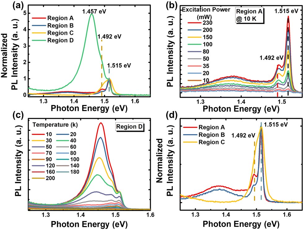 | ||
| Fig. 4 (a) Low temperature (10 K) normalized PL emission of GaAs nanowires grown on substrates with different etching times. (b) Power-dependent PL emission of GaAs nanowires grown on region A at low temperature (10 K). (c) Temperature-dependent PL spectra of GaAs nanowires grown on region D. (d) Normalized PL emission of regions A, B and C at low temperature (10 K). | ||
In addition, a closer look reveals that there is a high-energy band tail of the emission from samples in region C. Considering that the band gap of the GaAs WZ crystal phase is larger than that of ZB,53,54 we further perform peak fitting for the PL data of region C (results are not included in this paper), the high energy emission peak is located in 1.525 eV, which is consistent with that of the low-temperature WZ phase. It is believed that the high-energy band tail originates from the exciton recombination of the WZ crystal phase. The photon energy of the dominant peak for nanowires in region D is low (1.457 eV), and this emission peak is absent for other samples. During the temperature-dependent PL measurement, this peak rapidly disappears with the increase in temperature, as shown in Fig. 4(c). Therefore, this low-energy emission is considered to be from defects. Chen et al. observed a similar peak, which they attributed to a related recombination with an unknown deeper residual acceptor level.55 It is worth noting that a weak broad emission at 1.35–1.4 eV was observed in both samples A and B. First of all, Spirkoska et al.13 proposed that when the proportion of ZB phase in nanowires is reduced from 100% to 30%, the type II peak lies between 1.43 eV and 1.515 eV, so the correlation between the above luminescence peak and type II luminescence is excluded. Then, we analyze the PL with variable power, and we do not find that this peak follows the characteristic of type II luminescence, that is, the blue shift occurs with the increase in power. Then, by consulting the literature, it is found that the luminescence peak at 1.35–1.4 eV may be probably related to a transition involving the gallium vacancy level.56,57 Based on the above analysis, the intensity ratio of the emission at 1.515 to 1.492 eV can be used to describe the existence of WZ and ZB phases in different regions. The spectra of the three regions A, B and C are normalized as shown in Fig. 4(d). From the results of optical characterization, it can be inferred that the nanowires in the region B are dominated by the ZB crystal phase.
To further discuss the crystal phase of the materials, μ-Raman measurements were performed on a single nanowire which was mechanically transferred to a new Si substrate after ultrasonic cleaning. The Raman spectra of the GaAs nanowires grown in regions B and C are shown in Fig. 5(a) and (b), respectively. Compared to the nanowire grown in region B, four distinct scattering peaks can be observed in region C. To better discuss the origin of the diffraction peaks, a Lorentzian fitting was performed and the corresponding Raman scattering peaks are found to be around 256.9, 266.9–267.9, 288.2 and 291.5 cm−1, respectively. The diffraction peaks are correspondingly assigned to E2, TO, SO and LO, which are consistent with previous reports in the literature.58,59 Due to the small diameter of the nanowires, the peaks in the first-order Raman spectrum with frequencies between the TO and LO modes have been previously observed in several III-V nanowires and were identified as surface optical (SO) modes.60 Therefore, different from the ZB phase, the Raman spectrum of the WZ phase exhibits a unique scattering peak of the E2 mode. The XRD results of the corresponding nanowires are shown in Fig. 5(c) and (d), respectively. It can be seen that a GaAs-related diffraction peak appears on the left side of the Si(111) signal. For nanowires grown in region B, only the GaAs(111) peak can be found, and the corresponding peak position is 27.33° with a full-width half maximum (FWHM) of 0.145°. Two diffraction peaks, GaAs(002) and GaAs(111), can be observed in nanowires grown in region C, and the corresponding peak positions are 27.19 and 27.33°, and their FWHMs are 0.12 and 0.15°, respectively. Therefore, it can be confirmed that the WZ and ZB crystal phases coexist in the nanowires grown in region C.61
 | ||
| Fig. 5 (a) and (b) μ-Raman spectra of single GaAs nanowires grown in regions B and C, respectively. XRD spectra of (c) Region B and (d) Region C. | ||
Conclusions
In conclusion, we have obtained pure ZB phase GaAs nanowires by a simple substrate etching method. A series of GaAs nanowires with different densities and diameters were obtained. SEM, TEM, PL, Raman and XRD were used to characterize the nanowires grown on the substrate with different etching times under the same growth conditions. Analysis of the experimental results shows that the crystal phase in GaAs nanowires can be controlled by adjusting the size and density of the etched pinholes, combined with the shadowing effect to adjust the equivalent V/III flux ratio during the growth process. This work demonstrates the dynamics of the crystal phases in GaAs nanowires by simple substrate etching, which can be applied to other semiconductor nanowires, and facilitates the study of nanoscale devices.Author contributions
X. H. Wang, R. Chen and Z. P. Wei are responsible for the original conception of this work. The manuscript was prepared based on the research contributions from all the authors, namely J. L. Tang and Y. B. Kang are responsible for sample preparation, and S. Wang and H. L. Li performed the sample testing, data analysis, and the writing of the manuscript.Conflicts of interest
There are no conflicts to declare.Acknowledgements
This work is supported by the National Natural Science Foundation of China (11574130, 12074045, 62027820, 61904017, and 11804335), the Science, Technology and Innovation Commission of Shenzhen Municipality (Projects No. JCYJ20220530113015035, JCYJ20210324120204011 and KQTD2015071710313656), the Youth Foundation of Changchun University of Science and Technology (XQNJJ-2018-18), and the “111” Project of China (D17017).References
- K. Nakayama, K. Tanabe and H. A. Atwater, Appl. Phys. Lett., 2008, 93, 121904 CrossRef.
- U. Aeberhard, A. Gonzalo and J. M. Ulloa, Appl. Phys. Lett., 2018, 112, 213904 CrossRef.
- S. W. Eaton, A. Fu, A. B. Wong, C.-Z. Ning and P. Yang, Nat. Rev. Mater., 2016, 1, 16028 CrossRef CAS.
- E. Bermudez-Urena, G. Tutuncuoglu, J. Cuerda, C. L. Smith, J. Bravo-Abad, S. I. Bozhevolnyi, I. M. A. Fontcuberta, F. J. Garcia-Vidal and R. Quidant, Nano Lett., 2017, 17, 747–754 CrossRef CAS PubMed.
- J. Ho, J. Tatebayashi, S. Sergent, C. F. Fong, Y. Ota, S. Iwamoto and Y. Arakawa, Nano Lett., 2016, 16, 2845–2850 CrossRef CAS PubMed.
- X. Zhu, F. Lin, Z. Zhang, X. Chen, H. Huang, D. Wang, J. Tang, X. Fang, D. Fang, J. C. Ho, L. Liao and Z. Wei, Nano Lett., 2020, 20, 2654–2659 CrossRef CAS PubMed.
- K. Tomioka, J. Motohisa, S. Hara, K. Hiruma and T. Fukui, Nano Lett., 2010, 10, 1639–1644 CrossRef CAS PubMed.
- D. Thomson, A. Zilkie, J. E. Bowers, T. Komljenovic, G. T. Reed, L. Vivien, D. Marris-Morini, E. Cassan, L. Virot, J.-M. Fédéli, J.-M. Hartmann, J. H. Schmid, D.-X. Xu, F. Boeuf, P. O’Brien, G. Z. Mashanovich and M. Nedeljkovic, J. Opt., 2016, 18, 073003 CrossRef.
- J. Heinrich, A. Huggenberger, T. Heindel, S. Reitzenstein, S. Höfling, L. Worschech and A. Forchel, Appl. Phys. Lett., 2010, 96, 211117 CrossRef.
- X. Dai, S. Zhang, Z. Wang, G. Adamo, H. Liu, Y. Huang, C. Couteau and C. Soci, Nano Lett., 2014, 14, 2688–2693 CrossRef CAS PubMed.
- N. Erhard, S. Zenger, S. Morkotter, D. Rudolph, M. Weiss, H. J. Krenner, H. Karl, G. Abstreiter, J. J. Finley, G. Koblmuller and A. W. Holleitner, Nano Lett., 2015, 15, 6869–6874 CrossRef CAS PubMed.
- F. Glas, J. C. Harmand and G. Patriarche, Phys. Rev. Lett., 2007, 99, 146101 CrossRef PubMed.
- D. Spirkoska, J. Arbiol, A. Gustafsson, S. Conesa-Boj, F. Glas, I. Zardo, M. Heigoldt, M. H. Gass, A. L. Bleloch, S. Estrade, M. Kaniber, J. Rossler, F. Peiro, J. R. Morante, G. Abstreiter, L. Samuelson and A. Fontcuberta i Morral, Phys. Rev. B: Condens. Matter Mater. Phys., 2009, 80, 245325 CrossRef.
- C. B. Maliakkal, D. Jacobsson, M. Tornberg, A. R. Persson, J. Johansson, R. Wallenberg and K. A. Dick, Nat. Commun., 2019, 10, 4577 CrossRef CAS PubMed.
- S. Lehmann, J. Wallentin, E. K. Martensson, M. Ek, K. Deppert, K. A. Dick and M. T. Borgstrom, Nano Lett., 2019, 19, 2723–2730 CrossRef CAS PubMed.
- H. J. Joyce, J. Wong-Leung, Q. Gao, H. H. Tan and C. Jagadish, Nano Lett., 2010, 10, 908–915 CrossRef CAS PubMed.
- P. Krogstrup, R. Popovitz-Biro, E. Johnson, M. H. Madsen, J. Nygard and H. Shtrikman, Nano Lett., 2010, 10, 4475–4482 CrossRef CAS PubMed.
- S. Lehmann, J. Wallentin, D. Jacobsson, K. Deppert and K. A. Dick, Nano Lett., 2013, 13, 4099–4105 CrossRef CAS PubMed.
- F. Matteini, G. Tütüncüoglu, D. Mikulik, J. Vukajlovic-Plestina, H. Potts, J.-B. Leran, W. C. Carter and A. Fontcuberta i Morral, Cryst. Growth Des., 2016, 16, 5781–5786 CrossRef CAS.
- P. Schroth, J. Jakob, L. Feigl, S. M. Mostafavi Kashani, J. Vogel, J. Strempfer, T. F. Keller, U. Pietsch and T. Baumbach, Nano Lett., 2018, 18, 101–108 CrossRef CAS PubMed.
- J. Tersoff, Nano Lett., 2015, 15, 6609–6613 CrossRef CAS PubMed.
- V. G. Dubrovskii, N. V. Sibirev, J. C. Harmand and F. Glas, Phys. Rev. B: Condens. Matter Mater. Phys., 2008, 78, 235301 CrossRef.
- J. Vukajlovic-Plestina, W. Kim, L. Ghisalberti, G. Varnavides, G. Tutuncuoglu, H. Potts, M. Friedl, L. Guniat, W. C. Carter, V. G. Dubrovskii and I. M. A. Fontcuberta, Nat. Commun., 2019, 10, 869 CrossRef CAS PubMed.
- A. M. Raya, M. Friedl, S. Marti-Sanchez, V. G. Dubrovskii, L. Francaviglia, B. Alen, N. Morgan, G. Tutuncuoglu, Q. M. Ramasse, D. Fuster, J. M. Llorens, J. Arbiol and I. M. A. Fontcuberta, Nanoscale, 2020, 12, 815–824 RSC.
- F. Glas, J. C. Harmand and G. Patriarche, Phys. Rev. Lett., 2010, 104, 135501 CrossRef PubMed.
- J. Johansson, L. S. Karlsson, K. A. Dick, J. Bolinsson, B. A. Wacaser, K. Deppert and L. Samuelson, Cryst. Growth Des., 2008, 9, 766–773 CrossRef.
- H. J. Joyce, Q. Gao, H. H. Tan, C. Jagadish, Y. Kim, M. A. Fickenscher, S. Perera, T. B. Hoang, L. M. Smith, H. E. Jackson, J. M. Yarrison-Rice, X. Zhang and J. Zou, Adv. Funct. Mater., 2008, 18, 3794–3800 CrossRef CAS.
- M. Tchernycheva, J. C. Harmand, G. Patriarche, L. Travers and G. E. Cirlin, Nanotechnology, 2006, 17, 4025–4030 CrossRef CAS PubMed.
- D. P. Wilson, V. G. Dubrovskii and R. R. LaPierre, Nanotechnology, 2021, 32, 265301 CrossRef CAS PubMed.
- G. E. Cirlin, V. G. Dubrovskii, Yu. B. Samsonenko, A. D. Bouravleuv, K. Durose, Y. Y. Proskuryakov, B. Mendes, L. Bowen, M. A. Kaliteevski, R. A. Abram and D. Zeze, Phys. Rev. B: Condens. Matter Mater. Phys., 2010, 82, 035302 CrossRef.
- T. Dursap, M. Vettori, C. Botella, P. Regreny, N. Blanchard, M. Gendry, N. Chauvin, M. Bugnet, A. Danescu and J. Penuelas, Nanotechnology, 2021, 32, 155602 CrossRef CAS PubMed.
- V. G. Dubrovskii, T. Xu, A. Díaz Álvarez, S. R. Plissard, P. Caroff, F. Glas and B. Grandidier, Nano Lett., 2015, 15, 5580–5584 CrossRef CAS PubMed.
- V. G. Dubrovskii, W. Kim, V. Piazza, L. Güniat and A. Fontcuberta i Morral, Nano Lett., 2021, 21, 3139–3145 CrossRef CAS PubMed.
- M. Mattila, T. Hakkarainen, H. Lipsanen, H. Jiang and E. I. Kauppinen, Appl. Phys. Lett., 2006, 89, 063119 CrossRef.
- C. Colombo, D. Spirkoska, M. Frimmer, G. Abstreiter and A. Fontcuberta i Morral, Phys. Rev. B: Condens. Matter Mater. Phys., 2008, 77, 155326 CrossRef.
- S. L. Tan, Y. Genuist, M. I. den Hertog, E. Bellet-Amalric, H. Mariette and N. T. Pelekanos, Nanotechnology, 2017, 28, 255602 CrossRef PubMed.
- R. S. Wagner and W. C. Ellis, Appl. Phys. Lett., 1964, 4, 89–90 CrossRef CAS.
- A. Fontcuberta i Morral, C. Colombo, G. Abstreiter, J. Arbiol and J. R. Morante, Appl. Phys. Lett., 2008, 92, 063112 CrossRef.
- Y. Nitta, M. Shibata, K. Fujita and M. Ichikawa, Surf. Sci., 1999, 431, L565–L569 CrossRef CAS.
- F. Matteini, G. Tütüncüoglu, H. Potts, F. Jabeen and A. Fontcuberta i Morral, Cryst. Growth Des., 2015, 15, 3105–3109 CrossRef CAS.
- D. Rudolph, S. Hertenberger, S. Bolte, W. Paosangthong, D. Spirkoska, M. Doblinger, M. Bichler, J. J. Finley, G. Abstreiter and G. Koblmuller, Nano Lett., 2011, 11, 3848–3854 CrossRef CAS PubMed.
- G. Koblmuller, S. Hertenberger, K. Vizbaras, M. Bichler, F. Bao, J. P. Zhang and G. Abstreiter, Nanotechnology, 2010, 21, 365602 CrossRef CAS PubMed.
- D. Rudolph, L. Schweickert, S. Morkötter, B. Loitsch, S. Hertenberger, J. Becker, M. Bichler, G. Abstreiter, J. J. Finley and G. Koblmüller, Appl. Phys. Lett., 2014, 105, 069903 CrossRef.
- N. V. Sibirev, M. Tchernycheva, M. A. Timofeeva, J.-C. Harmand, G. E. Cirlin and V. G. Dubrovskii, J. Appl. Phys., 2012, 111, 104317 CrossRef.
- P. Schroth, M. Al Humaidi, L. Feigl, J. Jakob, A. Al Hassan, A. Davtyan, H. Kupers, A. Tahraoui, L. Geelhaar, U. Pietsch and T. Baumbach, Nano Lett., 2019, 19, 4263–4271 CrossRef CAS PubMed.
- L. E. Jensen, M. T. Björk, S. Jeppesen, A. I. Persson, B. Jonas Ohlsson and L. Samuelson, Nano Lett, 2004, 4, 1961–1964 CrossRef CAS.
- S. Hertenberger, D. Rudolph, M. Bichler, J. J. Finley, G. Abstreiter and G. Koblmüller, J. Appl. Phys., 2010, 108, 114316 CrossRef.
- M. T. Borgstrom, G. Immink, B. Ketelaars, R. Algra and E. P. Bakkers, Nat. Nanotechnol., 2007, 2, 541–544 CrossRef PubMed.
- L. T. T. Giang, C. Bougerol, H. Mariette and R. Songmuang, J. Cryst. Growth, 2013, 364, 118–122 CrossRef CAS.
- A. Senichev, P. Corfdir, O. Brandt, M. Ramsteiner, S. Breuer, J. Schilling, L. Geelhaar and P. Werner, Nano Res., 2018, 11, 4708–4721 CrossRef CAS.
- M. Jo, M. Sato, S. Miyamura, H. Sasakura, H. Kumano and I. Suemune, Nanoscale Res. Lett., 2012, 7, 654 CrossRef PubMed.
- S. V. Morozov, D. I. Kryzhkov, A. N. Yablonsky, A. V. Antonov, D. I. Kuritsin, D. M. Gaponova, Y. G. Sadofyev, N. Samal, V. I. Gavrilenko and Z. F. Krasilnik, J. Appl. Phys., 2013, 113, 163107 CrossRef.
- M. Hjort, S. Lehmann, J. Knutsson, R. Timm, D. Jacobsson, E. Lundgren, K. A. Dick and A. Mikkelsen, Nano Lett., 2013, 13, 4492–4498 CrossRef CAS PubMed.
- J. M. Jancu, K. Gauthron, L. Largeau, G. Patriarche, J. C. Harmand and P. Voisin, Appl. Phys. Lett., 2010, 97, 041910 CrossRef.
- Y. Chen, A. Freundlich, H. Kamada and G. Neu, Appl. Phys. Lett., 1989, 54, 45–47 CrossRef CAS.
- J. van de Ven, W. J. A. M. Hartmann and L. J. Giling, J. Appl. Phys., 1986, 60, 3735–3745 CrossRef CAS.
- D. Ruhstorfer, S. Mejia, M. Ramsteiner, M. Döblinger, H. Riedl, J. J. Finley and G. Koblmüller, Appl. Phys. Lett., 2020, 116, 052101 CrossRef CAS.
- I. Zardo, S. Conesa-Boj, F. Peiro, J. R. Morante, J. Arbiol, E. Uccelli, G. Abstreiter and A. Fontcuberta i Morral, Phys. Rev. B: Condens. Matter Mater. Phys., 2009, 80, 245324 CrossRef.
- T. A. Gant, H. Shen, J. R. Flemish, L. Fotiadis and M. Dutta, Appl. Phys. Lett., 1992, 60, 1453–1455 CrossRef CAS.
- C. García Núñez, A. F. Braña, J. L. Pau, D. Ghita, B. J. García, G. Shen, D. S. Wilbert, S. M. Kim and P. Kung, J. Appl. Phys., 2014, 115, 034307 CrossRef.
- W. Peng, F. Jabeen, B. Jusserand, J. C. Harmand and M. Bernard, Appl. Phys. Lett., 2012, 100, 073102 CrossRef.
| This journal is © The Royal Society of Chemistry 2023 |