
 Open Access Article
 This Open Access Article is licensed under a Creative Commons Attribution-Non Commercial 3.0 Unported Licence
Fabrication of low-cost and flexible perovskite solar cells by slot-die coating for indoor applications†
Cristina
Teixeira
 abc,
Rosinda
Fuentes-Pineda
a,
Luísa
Andrade
bc,
Adélio
Mendes
bc and
Dávid
Forgács
*a
abc,
Rosinda
Fuentes-Pineda
a,
Luísa
Andrade
bc,
Adélio
Mendes
bc and
Dávid
Forgács
*a
aSaule Technologies, Wroclaw Technology Park, 11 Dúnska Str., Sigma Building, Wroclaw, PL 54-427, Poland. E-mail: david.forgacs@sauletech.com
bLEPABE – Laboratory for Process Engineering, Environment, Biotechnology and Energy, Faculty of Engineering, University of Porto, Rua Dr. Roberto Frias, Porto, PT 4200-465, Portugal
cALiCE – Associate Laboratory in Chemical Engineering, Faculty of Engineering, University of Porto, Rua Dr. Roberto Frias, PT 4200-465 Porto, Portugal
First published on 3rd August 2023
Abstract
The fast progress of perovskite solar cells (PSCs) in terms of their photovoltaic performance under different lighting conditions, stability, and upscaling demonstrates the great potential of this technology to transit to the industrial scale. In particular, the performance of PSCs under low-light conditions has already surpassed the energy efficiency of the well-established amorphous silicon technology. However, PSC's industrialization will only be possible if the manufacturing process of the whole device is compatible with large-scale mass production. Here, we optimized an experimental procedure for fabricating flexible and low-cost PSCs under ambient atmosphere, low temperature, and high speed using only solution-based deposition techniques that are easy to upscale. An n–i device prepared by slot-die coating of SnO2 and perovskite layers and blade-coating a carbon electrode layer achieved a power conversion efficiency of 16.5% under 1000 lux and 6.9% under 1 sun. Using a 2D perovskite capping layer to passivate the 3D perovskite's surface defects, the power conversion efficiency increased to 18.6% under 1000 lux and to 7.7% under 1 sun. The 3D and 2D/3D hybrid perovskite devices lost 4% and 23%, respectively, of their initial efficiency after 550 h of operation at maximum power point tracking (MPPT) at 0.25 sun.
1. Introduction
Commonly, photovoltaic technologies are designed to maximize the conversion of sunlight into electricity. However, these technologies can also generate electricity under other lighting conditions, such as in space applications, where the light intensity is much higher, or in indoor environments, where the light sources are lamps with irradiances ∼300 times lower than sunlight (considering LED lamps with ∼1000 lux illuminance). In particular, perovskite solar cells (PSCs) have a great ability to convert any type of incident light into electricity. This happens because of the high absorption coefficient of perovskite materials and because their composition and dimensionality can be easily tuned to match the spectrum of the light source, thus maximizing the absorption of incident light.1If considering low-light conditions, perovskites represent a potential market disruptor since their photovoltaic performance surpasses that of the more-well-established amorphous silicon technology. Furthermore, the fabrication of consumer electronics powered by photovoltaics, such as the Internet of Things (IoT) systems, is growing exponentially, which represents a huge market opportunity for PSCs.2 To the best of the our knowledge, the highest power conversion efficiency (PCE) reported for amorphous silicon is 15.7% (under a 1.1 mW cm−2 LED lamp),3 while for PSCs it is 40.1% (under a 0.12 mW cm−2 LED lamp, glass substrate).4 However, the efficiencies are lower for PSCs fabricated on flexible substrates, where, due to their rough surface, low temperature resistance, and damage of the active layers due to mechanical deformation,5 the PCE can range between 31% for devices with an evaporated electrode, and 25% for the more industry-friendly all-solution-based devices (under a 0.4 mW cm−2 LED lamp).6
In addition to their high efficiencies, perovskite devices offer a range of benefits, such as the ability to be fabricated using low-cost and low-temperature solutions. This flexibility in manufacturing methods allows for the large-scale production of PSCs using simple and cost-effective methods, and the possibility of customizing the devices’ shape and design. Furthermore, if it successfully gets into the market, it will contribute to the PV market de-monopolization. Still, if we are moving toward the industrialization of perovskite devices, designing a stable device (materials and architecture) and developing a manufacturing process compatible with mass production are just as important as continuing to increase the efficiency. For instance, most of the high-efficiency PSCs are deposited using a small-scale deposition method, namely spin-coating, and have an expensive metallic back-contact deposited by evaporation under high vacuum. Ideally, the manufacturing process of the whole photovoltaic stack should be done under an ambient atmosphere, and using scalable and low-energy consumption techniques (i.e., low temperature and no requirement for a high vacuum).
Several large-scale deposition methods have already been developed, such as blade-coating, spray-coating, slot-die coating, and inkjet printing.7 However, one-step slot-die coating is currently the most promising one, given its straightforward integration into a roll-to-roll (R2R) system (which enables a high-throughput production capability), and the high photovoltaic performances already attained using this technique.8 In 2023, Jinzhao et al. reported an astonishing 22.3% efficiency in a 0.2 cm2 cell under 1 sun using a metal electrode and rigid substrate. Furthermore, encapsulated devices could withstand more than 1 year under continuous maximum power point tracking (MPPT) in outdoor real conditions, with virtually no decrease in efficiency.9 If considering only flexible substrates and processing under ambient atmosphere, moderately high efficiencies are still possible: in 2020, Watson's group reported a 13.4% efficiency for an n–i–p PSC with slot-die coated extraction layers and perovskite, and an evaporated electrode;10 while in 2023, the same group reported a 9.7% efficiency for a fully slot-die-coated device with a carbon-based electrode.11 Also, the latter devices could maintain ∼85% of their initial efficiency after 1000 h under 70% relative humidity with no encapsulation.11 However, there is currently no available data on the efficiency of flexible PSCs deposited exclusively by scalable deposition methods under indoor lighting conditions.
Here, we report the design and development of an experimental procedure to fabricate a flexible low-cost PSC based on slot-die coating focusing on mass production, as displayed in Fig. 1. The device architecture and the materials were selected to minimize the number of fabrication steps (depositions and treatments), minimize the energy consumption (low temperature and no need for a high vacuum), and maximize the stability of the device, without significantly compromising its PCE. The chosen architecture was a 4-layered planar device with metal oxide electron-transport materials, namely SnO2, mixed-halide 3D perovskite, (FAPbI3)0.85(MAPbBr3)0.15, 2D perovskite capping/passivation layer, n-octylammonium iodide (OAI), and carbon-based electrode (deposited by blade-coating).
 | ||
| Fig. 1 Illustration of the fabrication procedure optimized in this study, showing the slot-die coating of SnO2, 3D, and 2D perovskite layers, and blade coating of the carbon electrode layer. | ||
The solvent system of each material was carefully selected aiming at low viscosity, high volatility, and an appropriate polarity (for obtaining a stable solution with a uniform and fine particle-size distribution, and good adhesion with the underlying surface). The coating window of each material was determined using the viscocapillary model for the slot-die technique and the measured rheological data. According to the low flow limit plot, all the solutions formed a stable meniscus at the specified speed of 1 m min−1. The final optimized manufacturing process produced a PSC with a maximum PCE of 18.6% under 1000 lux (372 μW cm−2; 0.64 cm2 active area). The PSC with the bare 3D perovskite could maintain 96% of its initial efficiency after 550 h under MPPT under 0.25 sun, which demonstrates that the transition from the laboratory to fabrication of perovskite technology is definitely not that far in the future.
2. Experimental section
2.1 Materials
All the materials were used as received without further purification. The reactants used were lead iodide, PbI2 (Sigma-Aldrich, 99.9%), lead bromide, PbBr2 (Sigma-Aldrich, 98%), formamidinium iodide, FAI (Dyenamo, 99.99%), methylammonium bromide, MABr (Sigma-Aldrich, ≥99%), n-octylammonium iodide, OAI (Greatcell Solar, >99%), acetonitrile, ACN (Sigma-Aldrich, anhydrous 99.8%), 2-methoxyethanol, 2-ME (Sigma-Aldrich, anhydrous 99.8%), dimethyl sulfoxide, DMSO (Sigma-Aldrich, anhydrous ≥99%), 2-propanol, IPA (Sigma-Aldrich, anhydrous 99.5%), tin(IV) oxide, SnO2 (Alfa Aesar, 15% in H2O colloidal dispersion), and carbon paste (DN-CP01 from Dyenamo).2.2 Experimental procedure
![[thin space (1/6-em)]](https://www.rsc.org/images/entities/char_2009.gif) :40 v:v) to 1 wt%. A surfactant based on octyl-pyrrolidone (0.2 wt% with respect to SnO2 solution) was added to the final mixture. This was used as a shim 10 cm wide and 150 μm thick, together with a meniscus guide shim with a length of 800 μm. Before the coating, the PET/ITO surface was treated with N2 plasma for 2 min at a power of 75 W for 20 mL min−1 using a plasma system from PLASMA ETCH. The optimized parameters for the deposition of this solution were: 925 μm gap (distance between the substrate's top surface and the slot-die head lips), a speed of 1 m min−1, a pumping rate of 800 μL min−1 (wet film thickness of about 8 μm), and a bed temperature of 65 °C, followed by annealing at 100 °C for 45 min. For a faster annealing process, as is preferable in a R2R process, a 5 min long atmospheric pressure plasma can be used instead.12 The air-knife was not required for this deposition.
:2-ME 60:40 (v:v) according to the composition (FAPbI3)0.85(MAPbBr3)0.15. DMSO was added in a 50% molar ratio with respect to the perovskite solution. This solution was stirred for 3.5 h to ensure a good particle-size distribution (single peak 1.7 nm, see Fig. S2a (ESI†), and filtered with a 0.22 μm PTFE filter right before deposition.
:40 v:v) to 1 wt%. A surfactant based on octyl-pyrrolidone (0.2 wt% with respect to SnO2 solution) was added to the final mixture. This was used as a shim 10 cm wide and 150 μm thick, together with a meniscus guide shim with a length of 800 μm. Before the coating, the PET/ITO surface was treated with N2 plasma for 2 min at a power of 75 W for 20 mL min−1 using a plasma system from PLASMA ETCH. The optimized parameters for the deposition of this solution were: 925 μm gap (distance between the substrate's top surface and the slot-die head lips), a speed of 1 m min−1, a pumping rate of 800 μL min−1 (wet film thickness of about 8 μm), and a bed temperature of 65 °C, followed by annealing at 100 °C for 45 min. For a faster annealing process, as is preferable in a R2R process, a 5 min long atmospheric pressure plasma can be used instead.12 The air-knife was not required for this deposition.
:2-ME 60:40 (v:v) according to the composition (FAPbI3)0.85(MAPbBr3)0.15. DMSO was added in a 50% molar ratio with respect to the perovskite solution. This solution was stirred for 3.5 h to ensure a good particle-size distribution (single peak 1.7 nm, see Fig. S2a (ESI†), and filtered with a 0.22 μm PTFE filter right before deposition.
2.3 Characterization methods
3. Results and discussion
3.1 SnO2 dispersion
SnO2 is one of the most widely used materials for flexible planar n–i–p PSCs, given its high stability, low cost, and annealing temperature that is compatible with flexible substrates (lower than 140 °C).13 Furthermore, SnO2 is an aqueous-based colloidal dispersion, thus it poses no risk to health or the environment. To increase adhesion of the SnO2 dispersion to the PET/ITO surface and maximize the coating speed (or minimize the coating temperature), a volatile solvent, namely 2-propanol (IPA), was added into the dispersion. The maximum ratio of IPA in a 1% (wt) dispersion was 45% (v). Above this concentration, the SnO2 nanoparticles start agglomerating due to the change in pH from basic to neutral, resulting in a milky dispersion that is not suited for deposition, as shown in Fig. 2a.14 To prevent particle agglomeration, it is beneficial to keep the dispersion cold. We used 40% (v) IPA to ensure a better dispersion stability. To further increase the wettability of the dispersion on PET/ITO, a small amount of surfactant was added (0.17 μL mL−1). This amount of IPA and surfactant proved sufficient to reduce the contact angle from 31° to 17° (after 2 min N2 plasma treatment of the PET/ITO substrate), see Table S2 (ESI†). | ||
| Fig. 2 (a) SnO2 dispersion with different water:IPA ratios, and (b) perovskite solutions with different ACN:2-ME ratios. | ||
3.2 3D perovskite solution
The perovskite composition has a major impact on the photovoltaic performance and stability of the final device. Theoretically, wide-bandgap perovskites offer the potential for higher efficiencies under low-light conditions, since they have a better overlap with the spectrum of the lamps and are capable of generating a higher photovoltage.15 Usually adding bromide to the perovskite composition widens the bandgap of perovskite materials; however, it compromises their stability due to phase segregation triggered by light soaking, particularly for bromide molar ratios higher than 0.2.16 This effect can be significantly reduced by adding a specific amount of cesium salt to the perovskite composition, for instance, in a ratio of 0.17 of cesium (0.83 formamidinium) when using 0.30 of bromide (0.70 iodide).17 However, due to their significant solubility challenges in common perovskite solvents (particularly cesium salts) and their limited coating window for obtaining high-quality perovskite films, it is preferable to avoid cesium and to minimize the bromide content in slot-die coating processes.18 Using a low methylammonium concentration is also preferable given its low stability to humidity and high volatility. Previous studies confirmed the suitability of the (FAPbI3)0.85(MAPbBr3)0.15 composition for large-scale deposition techniques under an ambient atmosphere, and exhibited an improved operational stability for over 1000 h in outdoor conditions.19–21 Thus, despite the lower bandgap (1.61 eV), this composition was chosen for the present work.Tuning the physicochemical and rheological properties of the solvents is essential for obtaining a high-quality film by slot-die coating. To achieve an optimal and safe perovskite deposition with a high coating speed and low temperature, the solvents should have high volatility, low viscosity, and proper polarity (for effective perovskite solubilization without harming the underlying layer), and low toxicity. Acetonitrile (ACN) presents a viable option, yet without the addition of other solvents, it leads to perovskite precipitation. In this regard, adding 2-methoxyethanol (2-ME), even though it is not classified as a green solvent, hinders perovskite precipitation: the minimum amount required is 40% (v) for a 0.6 M solution, see Fig. 2b. In fact, the ratio of ACN:2-ME of 60:40 (v:v) has already been demonstrated to be a good solvent mixture for large-scale coating techniques at room temperature.22 Furthermore, DMSO was used here as an additive (with a molar concentration of 50% of the perovskite, i.e., 0.3 M), since its high coordination ability with the perovskite could lead to an enhancement of the perovskite crystallinity and better adhesion to the underlying layer.22
3.3 2D perovskite solution
The free charge-carrier density generated with indoor lamps is significantly lower than the density generated at 1 sun (irradiance is ∼300 times lower at low light). Thus, the recombination within the trap sites present in a PSC has a much greater impact on the photovoltaic performance under low-light conditions. In particular, a major part of this recombination happens at the perovskite crystal surface due to the high density of crystallographic imperfections, such as uncoordinated sites (Pb+, I−), uncoordinated ions (Pb2+, I−, or Br−), Pb clusters, and organic cation vacancies.23 Coating an ultra-thin layer of long-chain organic cations on top of the perovskite surface to form a hybrid 2D/3D perovskite layer is a promising way to passivate these defects while simultaneously creating a “moisture shielding” effect that enhances the ambient stability. These spacer cations replace MA+ and FA+ sites, forming a 2D perovskite layer.24 It is important to ensure that the solvent used to dissolve the 2D spacer organic cation does not damage the 3D perovskite, thus a test was done here using six different solvent systems, see Fig. S4a (ESI†). IPA was selected given its low toxicity, high volatility, relatively low viscosity, and proper polarity. The most relevant properties of the solvents are presented in Table S1 (ESI†).Also, in a preliminary study, six long-chain ammonium iodides were selected and deposited by blade-coating (each with the same molarity and ensuring the best possible approximation to the slot-die conditions/parameters): n-octylammonium iodide (OAI), phenethylammonium iodide (PEAI), 2-thiophene methylammonium iodide (ThMAI), 4-fluoro-phenethylammonium iodide (4FPEAI), n-butylammonium iodide (BAI), and 5-ammonium valeric acid iodide (5-AVAI). XRD data confirmed the presence of a 2D perovskite phase for all the organic salts (XRD peaks located between 4.4° and 8.8°), see Fig. S4b (ESI†).25 However, the intensity of the 2D peak for the OAI salt was much higher than the 2D peaks for the other salts, which indicated that the 2D layer of OAI had a higher crystalline structure. Indeed, this was the sample that provided the best photovoltaic performance both at 1000 lux and 1 sun, see Fig. 3. In general, spacer cations with longer alkyl chains and higher hydrophobicity, such as octylammonium (OA+), have been shown to be more efficient in reducing defects, improving charge transport, and enhancing device performance.26
 | ||
| Fig. 3 (a) JV curves of slot-die coated samples with each 2D perovskite salt at (a) 1000 lux and (b) 1 sun with the respective PCE values in the reverse and forward scans; (c) and stabilized power output at 1 sun; and (d) molecular structure of the six long-chain alkylammonium iodides selected for the 2D perovskite. | ||
3.4 Pretreatment
Functionalizing the substrate surface by removing organic contaminants and adding specific functional groups can greatly enhance the solution's adhesion to the substrate, resulting in a high-quality growth of the coated material.27 Furthermore, according to the viscocapillary model of the slot-die coating technique, increasing the surface energy of the coating surface results in a wider coating window, i.e., its broadens the range of possible variables for the rheology and operating parameters.28 Two of the most used techniques for the ultrafine cleaning and functionalization of surfaces are N2 plasma and UV/ozone treatment.29To understand the impact of each surface modification treatment on the quality of the coating, SnO2 and perovskite solutions were coated on PET/ITO and SnO2 (respectively), before and after N2 plasma and UV/ozone treatment, see Fig. S5 (ESI†). To avoid any damage to the 3D perovskite surface, the 2D solution was coated on perovskite with no treatment. In fact, the contact angle of OAI in IPA on 3D perovskite was so low that there was no need to modify the surface energy. The contact angle values and images of each configuration are presented in Table S2 (ESI†) and Table 1, respectively.
| Contact angle | |||
|---|---|---|---|
| Pretreatment | None | 15 min UV/ozone | 2 min N2 plasma |
| SnO2 solution on PET |

|

|

|
| 3D perovskite solution on SnO2 |

|

|

|
| 2D perovskite solution on 3D perovskite |

|
||
| Surface energy [mN m−1] | ||||
|---|---|---|---|---|
| Substrate | Treatment | Polar component | Dispersive component | Total |
| PET | None | 13.74 | 33.49 | 47.23 |
| UV/ozone | 20.28 | 33.94 | 54.21 | |
| N2 plasma | 26.62 | 43.29 | 69.91 | |
| SnO2 | None | 24.71 | 40.89 | 65.60 |
| UV/ozone | 34.17 | 40.55 | 74.72 | |
| N2 plasma | 33.99 | 43.59 | 77.58 | |
Also, the contact angles of diiodomethane and water on each substrate before and after the surface treatments were also determined in order calculate the surface energy by the Owens, Wendt, Rabel, and Kaelble (OWRK) method, see Table 1.30 Here, the total surface energy corresponds to the sum of the polar and the dispersive components. Since water reacts with the perovskite, and given the similar contact angle results, the surface energy of the perovskite surface with no treatment was assumed to be close to that of the N2 plasma-treated SnO2.
The low surface energy of PET/ITO (47 mN m−1) resulted in a very high contact angle with the SnO2 solution (33°), and consequently the freshly coated SnO2 film (even with a small amount of surfactant) de-wetted before reaching the saturation point, resulting in a film with very low coverage and uniformity, see Fig. S5a (ESI†). Removing the organic contaminants from this surface by applying 15 min UV/ozone resulted in increasing the polar component of the surface energy by 48%, but had virtually no effect on the dispersive component. Overall, the total surface energy increased only by 15%, which was not enough to avoid de-wetting. On the other hand, N2 plasma increased both the polar and dispersive components by 94% and 29%, respectively, for a total increase/decrease of 48% in the surface energy/contact angle, which enabled the coating of a highly uniform SnO2 film. Apart from the surface ultrafine cleaning, N2 plasma triggered the co-generation of N2 doping species and oxygen vacancies on the surface, which was the most likely cause of the significant surface energy modification.31 Regarding the SnO2 film, it already presented a high surface energy (66 mN m−1), and perovskite could be grown on this layer without any treatment, see Fig. S5b (ESI†). Interestingly, exposing the SnO2 surface to UV/ozone resulted in a higher contact angle of the 3D perovskite solution, which may be because the long hydrophobic chains of the surfactant might have been broken by the ozone generated by the UV light, thus decreasing the intermolecular forces between the SnO2 layer and the 3D perovskite solution, leading to a slight decrease in the dispersive component. On the other hand, N2 plasma pretreatment did not damage the surfactant molecules, and actually it increased the surface energy by 18% and might even enhance its structural, optical, and electrical properties.32 Thus, N2 plasma pretreatment was employed to have a more flexible coating window.
3.5 Slot-die coating
Before coating the optimized solutions, the viscocapillary model of slot-die coating was used to determine the ranges of the operating parameters (volumetric pumping rate, coating speed, meniscus guide length, and gap) that would still produce a stable meniscus and high-quality defect-free film.33 The capillary number (Ca) is a dimensionless quantity that represents the ratio between the viscous forces and the surface tension forces of a specific solution. It can be obtained by using eqn (1):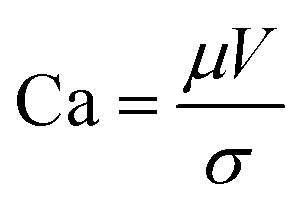 | (1) |
 | (2) |
 | (3) |
 | ||
| Fig. 4 Low flow limit model for the SnO2, 3D, and 2D perovskite solutions, and the respective capillary numbers. Inset table: rheological and operational parameters for each solution and the low flow limit values obtained with the viscocapillary model. | ||
The maximum coating speeds for the SnO2, 3D perovskite, and 2D perovskite were 3.0, 3.3, and 1.6 m min−1. It is interesting to note that the maximum coating speed for SnO2 was almost twice that of the 2D perovskite, despite the very similar rheological parameters (viscosity and surface energy). This was due to the lower wet film thickness of the 2D perovskite and clearly shows that a way for increasing the coating speed is by increasing the wet film thickness and decreasing the concentration of the solution, so the same final dry film thickness could be achieved. Still, another way to increase the coating speed is by adjusting the solvent system to decrease the viscosity of the solution, where the 3D perovskite solution has a thinner wet film than SnO2 dispersion and still has a similar maximum coating speed due to the lower viscosity. If solutions (solvent system and concentration) cannot be changed, decreasing the gap enables the use of higher coating speeds and thinner wet films without compromising the meniscus stability. Additionally, if the coating window is still too narrow, stronger surface treatments and additives (such as surfactants) can be employed. Overall, in the slot-die coating technique, the large number of variables and the interplay between them makes it difficult and time-consuming to achieve consistent and high-quality coatings. Thus, to overcome this challenge it is often necessary to fix some variables and cautiously design a set of experiments that would allow optimizing the remaining variables.
To mimic an R2R process, the coating speed was set to 1 m min−1. At this speed, a coating temperature of 65 °C was required to ensure a good drying of the SnO2 solution, whereby the solvent evaporated and SnO2 film formed uniformly ∼5 cm behind the slot-die head (experimentally verified). The pumping rate was defined to obtain an 8 μm wet film thickness, which corresponded to 800 μL min−1 (coating width was 10 cm). This was the ideal wet film thickness for obtaining a compact ∼40 nm-thick SnO2.
For the 3D perovskite deposition, the coating bed was kept at room temperature, (26 ± 1) °C, and an air-knife was assembled on to the coater, with a fixed N2 flow of 75 L min−1. To reduce the wet film disturbance by the strong impact of the N2 flow from the air-knife, a toll was used to change the flow direction from perpendicular to parallel to the surface. This strategy minimized chatter defects without compromising the fast evaporation rate. Chatter defects refer to the periodic variations in the thickness of the coated layer along the coating direction that appear at regular intervals.34
Preliminary studies demonstrated that, with the selected operational parameters and solution, an ideal thickness of ∼500 nm was obtained with a wet film thickness of 5–6 μm (pumping rate of 500–600 μL min−1), see Fig. 5. For a thinner wet film, the light absorption would decrease, reducing the density of photogenerated charge carriers and consequently the current density produced, while for thicker wet films the roughness would start increasing and the photovoltaic performance would slightly decrease due to the higher density of trap-assisted recombination sites.
 | ||
| Fig. 5 (a) JV curves, (b) photovoltaic parameters, and (c) SEM cross section images of the slot-die coated 3D perovskite film with different wet film thickness: 3–4 μm, 5–6 μm, and 7–8 μm. | ||
In the case of OAI, since it is an insulating long-chain salt, the thickness of the wet film was minimized to reduce the resistance to charge transfer at that interface with the 3D perovskite. According to the low flow limit plot, at 1 m min−1, the minimum wet film thickness that would not compromise the meniscus stability was 2.2 μm. To have a more comfortable coating window, the wet film thickness was set to 3 μm, with a pumping rate of 270 μL min−1 (coating width of 9 cm). The XRD data, see Fig. 6e, confirmed the presence of the 2D perovskite phase, where the 2 peaks at 3.7° and 4.3° corresponded to the (020) crystal plane characteristic of 2D perovskite with a dimensionality of 2–3.25 Still, the obtained layer was so thin that could barely be noticed in the cross-section SEM images, see Fig. 6b, and it had no influence in the absorption spectrum, see Fig. 6c.
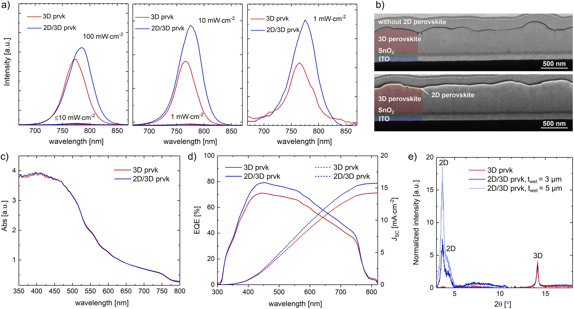 | ||
| Fig. 6 Characterization data comparing the properties of the 3D perovskite and 2D/3D hybrid perovskite layers: (a) photoluminescence spectrum at different light intensities (1, 10, and 100 mW cm−2), (b) SEM cross-section images, (c) UV-visible absorption spectrum, (d) external quantum efficiency spectrum and respective cumulative current density, and (e) X-ray diffraction spectrum. | ||
3.6 Carbon deposition
The high viscosity of the commercial carbon paste makes it extremely difficult to deposit by slot-die coating. It was thus deposited by blade-coating, resulting in a thickness of 15 μm, see Fig. S7 (ESI†). Future work will include the development of highly conductive carbon paste with low viscosity for solar cell applications. Another alternative is to optimize the carbon deposition by screen-printing, since this process can be also integrated in an R2R process.3.7 Characterization
Adding the 2D perovskite layer resulted in an increase in the photoluminescence (PL) peak height both at low and high irradiance levels, which indicates that the 2D layer did passivate the surface defects, extending the charge-carrier lifetime by reducing the recombination pathways. This passivating effect was more noticeable for lower light intensities, which was expected given the greatest impact of the trap sites at this light range, and it had an even positive impact throughout the whole spectrum, as confirmed by the external quantum efficiency EQE data, see Fig. 6d. The photoluminescence (PL) peak of 3D perovskite corresponded to a bandgap of 1.61 eV, which is in accordance with the values presented in the literature for the selected perovskite formulation, see Fig. 6a.20 The quantum confinement effect of the 2D perovskite should result in an increase in the bandgap.35 However, the PL peaks were shifted toward higher wavelengths and the bandgap decreased to 1.59 eV after the 2D perovskite passivation.The formulated hypothesis is that during the 2D perovskite coating, the 3D perovskite surface is dissolved by the IPA solvent, and when it recrystallizes back together with the OAI molecule, the surface becomes smoother, enhancing in this way the contact with carbon and the carrier-charge extraction, and the surface defects, like ion vacancies, uncoordinated sites, and dangling bonds, are healed, increasing the PL peak height. This new structure will also have a higher amount of iodide, which then decreases the bandgap. The larger radius of iodide and lower electronegativity causes an increase in the energy required to excite an electron from the valence band to the conduction band, i.e., the bandgap.36
Interestingly, the increases in power conversion efficiency due to this surface passivation at 1000 lux and 1 sun were both ∼10%: from 16.5% to 18.6% at 1000 lux (372.2 μW cm−2), and from 6.9% to 7.7% at 1 sun, see Fig. 7a and b. Box charts of the photovoltaic parameters of the samples with and without the 2D perovskite layer under 1000 lux and 1 sun are presented in Fig. 7e and Fig. S6 (ESI†), respectively. The PCE increase was mainly caused by the higher photogenerated current density, which might be caused by the enhanced contact with the carbon layer after the recrystallization. Regarding the stability, the device without the 2D layer kept 92% of its initial PCE after 550 h at maximum power point tracking under 25 mW cm−2 inside a N2-filled glovebox. Adding the 2D perovskite layer worsened the operational stability by ∼20% (the device kept only 71% of its initial PCE), see Fig. 7d. Although 2D perovskite capping layers are known to increase the stability to moisture, they might compromise the long-term operational stability due to the ionic diffusion between these two layers, triggered and accelerated by constantly stressing the samples with light exposure and the applied electrical field. According to Luo et al.,37 after long time exposure to these stressing factors, the 2D perovskite layer can totally merge with the 3D perovskite layer, creating a disorganized 2D/3D perovskite heterostructure with high defect density, which is responsible for the efficiency loss.
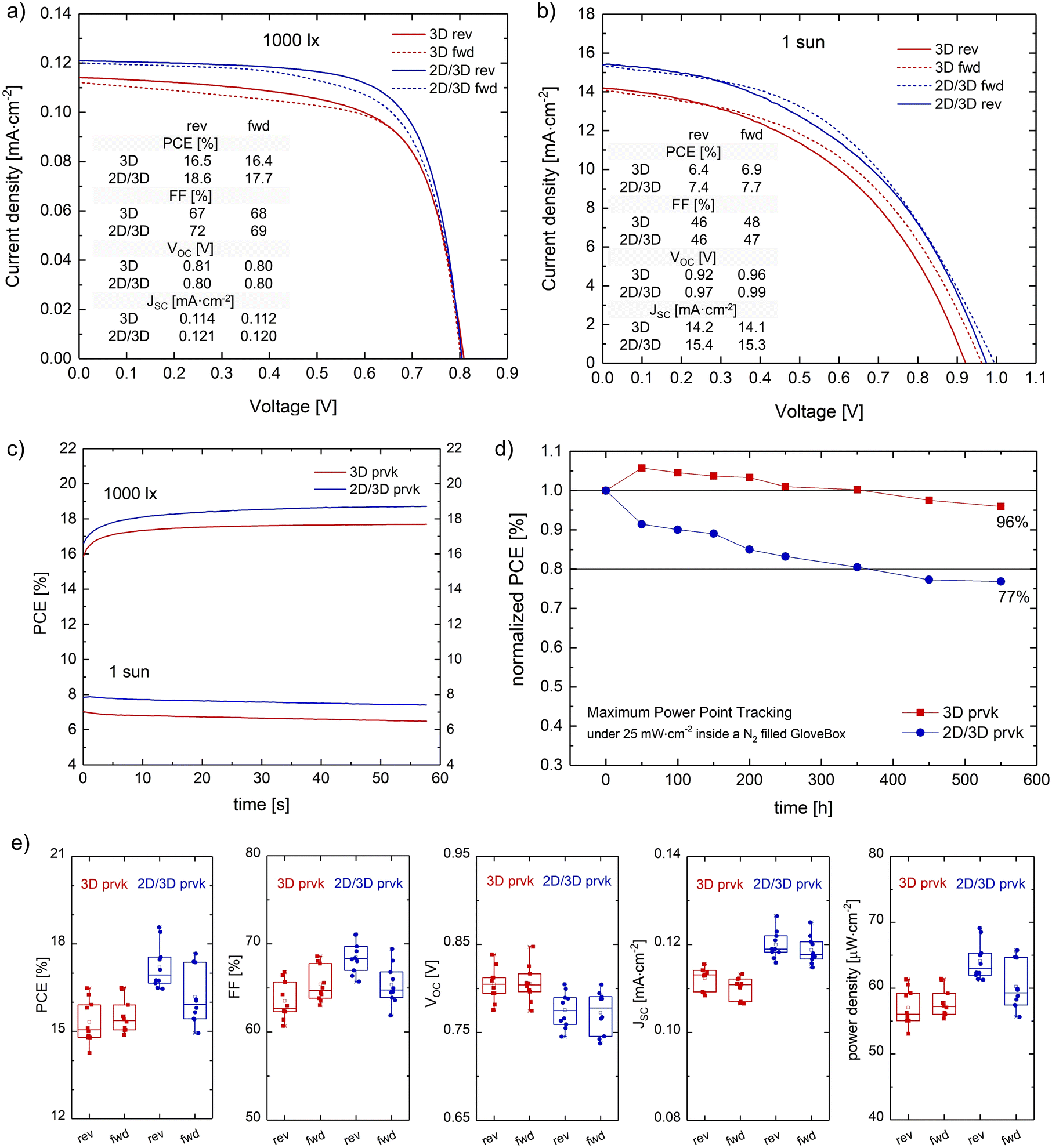 | ||
| Fig. 7 Comparison of the photovoltaic performance and operational stability of devices with 3D perovskite and 2D/3D perovskite: J–V curves at reverse and forwards scan at (a) 1000 lux and (b) 1 sun and respective photovoltaic parameters; (c) stabilized power output at 1000 lux and 1 sun during 55 s; (d) MPPT test under 25 mW cm−2 inside a N2-filled glovebox for 550 h; and (e) box charts of the photovoltaic parameters of 10 samples. | ||
4. Conclusion
A procedure for the fabrication of flexible and low-cost perovskite solar devices using a slot-die coating technique was described. The architecture and materials were selected to minimize the number of fabrication steps, energy consumption, and maximize stability and performance. The fabrication process involved coating a metal oxide electron-transport material, a mixed-halide 3D perovskite, a 2D perovskite capping/passivation layer, and a carbon-based electrode. The 2D perovskite layer was studied using six different spacer cations, and it was found that n-octylammonium iodide (OAI) salt yielded the best performance due to its longer alkyl chain and higher hydrophobicity. Surface treatments and coating windows for each material were determined according to the viscocapillary model for the slot-die technique, and the final optimized fabrication procedure resulted in a perovskite solar cell with a maximum PCE of 18.6% at 1000 lux and 7.7% at 1 sun. Furthermore, the 3D perovskite device kept 96% of its initial efficiency after 550 h of testing under maximum power point tracking. Surprisingly, adding a 2D layer worsened the long-term stability, likely due to the accelerated ion diffusion between the 2D and 3D perovskite layers.Conflicts of interest
There are no conflicts to declare.Acknowledgements
Cristina Teixeira and Dávid Forgács acknowledge funding from the European Regional Development funds provided by the National Centre of Research and Development (NCBR) under POIR.01.01.01-00-1482/19-00. Luísa Andrade and Adélio Mendes acknowledge Project InPSC (PTDC/EQU-EQU/4193/2021), LA/P/0045/2020 (ALiCE), UIDB/00511/2020 and UIDP/00511/2020 (LEPABE), all supported by national funds through FCT/MCTES (PIDDAC). The authors also acknowledge the support of Dr Vivek Babu, Dr Mario Escobar, Dr Felipe Vinocour, and Dr Pierpaolo Spinelli in the experimental procedure development.References
- A. S. R. Bati, Y. L. Zhong, P. L. Burn, M. K. Nazeeruddin, P. E. Shaw and M. Batmunkh, Commun. Mater., 2023, 4, 2 CrossRef CAS.
- M. Hasan, IoT Analytics [Online], 2022, https://iot-analytics.com/numberconnected-iot-devices/.
- P. C. Yang, I. M. Chan, C. H. Lin and Y. L. Chang, 37th IEEE Photovoltaic Specialists Conference, 2011, 000696 Search PubMed.
- X. He, J. Chen, X. Ren, L. Zhang, Y. Liu, J. Feng, J. Fang, K. Zhao and S. Liu, Adv. Mater., 2021, 33, 2100770 CrossRef CAS PubMed.
- C.-H. Chen, Z.-H. Su, Y.-H. Lou, Y.-J. Yu, K.-L. Wang, G.-L. Liu, Y.-R. Shi, J. Chen, J.-J. Cao, L. Zhang, X.-Y. Gao and Z.-K. Wang, Adv. Mater., 2022, 34, 2200320 CrossRef CAS PubMed.
- C. Teixeira, P. Spinelli, L. A. Castriotta, D. Müller, S. Öz, L. Andrade, A. Mendes, A. D. Carlo, U. Würfel, K. Wojciechowski and D. Forgács, Adv. Funct. Mater., 2022, 32, 2206761 CrossRef CAS.
- Z. Li, T. R. Klein, D. H. Kim, M. Yang, J. J. Berry, M. F. A. M. van Hest and K. Zhu, Nat. Rev. Mater., 2018, 3, 18017 CrossRef CAS.
- Y. Tu, J. Ye, G. Yang, Y. Zang, L. Zhang, Y. Wang, G. Li, L. Chu and W. Yan, J. Alloys Compd., 2023, 942, 169104 CrossRef CAS.
- J. Li, J. Dagar, O. Shargaieva, O. Maus, M. Remec, Q. Emery, M. Khenkin, C. Ulbrich, F. Akhundova, J. A. Márquez, T. Unold, M. Fenske, C. Schultz, B. Stegemann, A. Al-Ashouri, S. Albrecht, A. T. Esteves, L. Korte, H. Köbler, A. Abate, D. M. Többens, I. Zizak, E. J. W. List-Kratochvil, R. Schlatmann and E. Unger, Adv. Energy Mater., 2023, 2203898 CrossRef.
- D. Burkitt, R. Patidar, P. Greenwood, K. Hooper, J. McGettrick, S. Dimitrov, M. Colombo, V. Stoichkov, D. Richards, D. Beynon, M. Davies and T. Watson, Sustainable Energy Fuels, 2020, 4, 3340–3351 RSC.
- D. Beynon, E. Parvazian, K. Hooper, J. McGettrick, R. Patidar, T. Dunlop, Z. Wei, P. Davies, R. Garcia-Rodriguez, M. Carnie, M. Davies and T. Watson, Adv. Mater., 2023, 2208561 CrossRef CAS PubMed.
- M. Shekargoftar, J. Pospisil, M. Kratochvíl, J. Vida, P. Souček and T. Homola, Energy Technol., 2021, 9, 2001076 CrossRef CAS.
- A. Uddin and H. Yi, Sol. RRL, 2022, 6, 2100983 CrossRef CAS.
- D. Richards, D. Burkitt, R. Patidar, D. Beynon and T. Watson, Mater. Adv., 2022, 3, 8588–8596 RSC.
- M. Freunek, M. Freunek and L. M. Reindl, IEEE J. Photovoltaics, 2013, 3, 59–64 Search PubMed.
- S. Draguta, O. Sharia, S. J. Yoon, M. C. Brennan, Y. V. Morozov, J. S. Manser, P. V. Kamat, W. F. Schneider and M. Kuno, Nat. Commun., 2017, 8, 200 CrossRef PubMed.
- A. J. Knight, J. Borchert, R. D. J. Oliver, J. B. Patel, P. G. Radaelli, H. J. Snaith, M. B. Johnston and L. M. Herz, ACS Energy Lett., 2021, 6, 799–808 CrossRef CAS PubMed.
- X. Wan, Z. Yu, W. Tian, F. Huang, S. Jin, X. Yang, Y.-B. Cheng, A. Hagfeldt and L. Sun, J. Energy Chem., 2020, 46, 8–15 CrossRef.
- M. He, B. Li, X. Cui, B. Jiang, Y. He, Y. Chen, D. O’Neil, P. Szymanski, M. A. Ei-Sayed, J. Huang and Z. Lin, Nat. Commun., 2017, 8, 16045 CrossRef CAS PubMed.
- P. W.-K. Fong, H. Hu, Z. Ren, K. Liu, L. Cui, T. Bi, Q. Liang, Z. Wu, J. Hao and G. Li, Adv. Sci., 2021, 8, 2003359 CrossRef CAS PubMed.
- Y. Reyna, M. Salado, S. Kazim, A. Pérez-Tomas, S. Ahmad and M. Lira-Cantu, Nano Energy, 2016, 30, 570–579 CrossRef CAS.
- Y. Deng, C. H. Van Brackle, X. Dai, J. Zhao, B. Chen and J. Huang, Sci. Adv., 2019, 5, eaax7537 CrossRef CAS PubMed.
- H. Lu, A. Krishna, S. M. Zakeeruddin, M. Grätzel and A. Hagfeldt, iScience, 2020, 23, 101359 CrossRef CAS PubMed.
- T. M. Koh, V. Shanmugam, X. Guo, S. S. Lim, O. Filonik, E. M. Herzig, P. Müller-Buschbaum, V. Swamy, S. T. Chien, S. G. Mhaisalkar and N. Mathews, J. Mater. Chem. A, 2018, 6, 2122–2128 RSC.
- Y.-H. Chang, J.-C. Lin, Y.-C. Chen, T.-R. Kuo and D.-Y. Wang, Nanoscale Res. Lett., 2018, 13, 247 CrossRef PubMed.
- H. S. Choi and H. S. Kim, Materials, 2020, 13, 3868 CrossRef CAS.
- D. Hegemann, H. Brunner and C. Oehr, Nuclear Instruments and Methods in Physics Research Section B: Beam Interactions with Materials and Atoms, 2003, 208, 281–286 CrossRef CAS.
- X. Ding, J. Liu and T. A. L. Harris, AIChE J., 2016, 62, 2508–2524 CrossRef CAS.
- D. P. Nicole Zander and B. Stein, Oxidation of Polyethylene: A Comparison of Plasma and Ultraviolet Ozone Processing Techniques, Defense Technical Information Center, 2009.
- M. Annamalai, K. Gopinadhan, S. A. Han, S. Saha, H. J. Park, E. B. Cho, B. Kumar, A. Patra, S.-W. Kim and T. Venkatesan, Nanoscale, 2016, 8, 5764–5770 RSC.
- J. Ji-Won, J. E. E. Hyeok and S. E. O. Hye-Won, NPSM, 2020, 70, 103–106 CrossRef.
- M. Medhat, H. M. El-Sayed, M. A. Saudy and M. Saleh, Egypt J. Solids, 2011, 34, 7–18 CrossRef.
- M. S. Carvalho and H. S. Kheshgi, AIChE J., 2000, 46, 1907–1917 CrossRef CAS.
- Ossila, Slot-Die Coating: Theory, Design, & Applications, https://www.ossila.com/en-pl/pages/slot-die-coating-theory.
- M. Saffari, H. R. Soleimani and M. B. Tagani, Phys. E, 2020, 124, 114226 CrossRef CAS.
- C. Lin, S. Li, W. Zhang, C. Shao and Z. Yang, ACS Appl. Energy Mater., 2018, 1, 1374–1380 CrossRef CAS.
- L. Luo, H. Zeng, Z. Wang, M. Li, S. You, B. Chen, A. Maxwell, Q. An, L. Cui, D. Luo, J. Hu, S. Li, X. Cai, W. Li, L. Li, R. Guo, R. Huang, W. Liang, Z.-H. Lu, L. Mai, Y. Rong, E. H. Sargent and X. Li, Nat. Energy, 2023, 8, 294–303 CrossRef CAS.
Footnote |
| † Electronic supplementary information (ESI) available. See DOI: https://doi.org/10.1039/d3ma00285c |
| This journal is © The Royal Society of Chemistry 2023 |