
 Open Access Article
 This Open Access Article is licensed under a
 Creative Commons Attribution 3.0 Unported Licence
The effect of the TiO2 interface layer on the electrochromic properties of WO3-based devices†
Panshu
Gui‡
a,
Ziyi
Jin‡
a,
Yufeng
Bai
a,
Zhengqiao
Lv
a,
Jianwei
Mo
a,
Shuai
Chang
 b and
Di
Yang
*a
b and
Di
Yang
*a
aSchool of Science, Minzu University of China, Beijing 100081, China. E-mail: diyang@muc.edu.cn
bDepartment of Materials Science, Shenzhen MSU-BIT University, Shenzhen, China. E-mail: schang@smbu.edu.cn
First published on 25th July 2023
Abstract
Herein, using DC magnetron sputtering technology, smooth and dense WO3 films and WO3/TiO2 composite films were successfully prepared under the optimized preparation conditions. Subsequently, electrochromic devices (EC) and photoelectrochemical devices (PEC) were fabricated with a sputtering deposition time of 30 min for the WO3 film and different deposition times for the TiO2 interface layer. The TiO2 interface layers deposited with a sputtering time of 2–3 min were proven to improve the electrochromic properties of the devices. Specifically, compared with the WO3-based EC devices, the WO3/TiO2-based EC devices exhibited a higher transmittance in the bleached sate and much lower transmittance in the coloured state, resulting in a wider transmission modulation range. For instance, the modulation range of the WO3/TiO2-based EC devices reached 73.9% at 600 nm, which is larger than that of the WO3-based EC devices (62.5%). Optical measurements revealed that the TiO2 interface layer reduced the amount of undesirable localized states by protecting WO3, while increasing the amount of Li+ ions embedded in WO3 for device colouration. This was further demonstrated by cyclic voltammetry measurements. The optimized TiO2 interface layer significantly increased the inserted Li+ ion density and extracted Li+ ion density. Interestingly, the difference between the inserted and extracted charge density was obviously reduced after the introduction of the TiO2 interface layer. This indicated that the WO3/TiO2-based EC devices possessed good cycling stability, which is due to the fact that the surface of WO3 was passivated by TiO2, and thus its surface state was not subject to corrosion by the electrolyte and the formation of irreversible interface states was suppressed. Additionally, PEC devices were successfully fabricated based on WO3/TiO2 films to investigate their electrochromic characteristics under a small self-driving power. Consequently, driven by the integrated photovoltaic film, the PEC device exhibited a large transmission modulation in the wavelength range from 500 nm to 1800 nm, and especially in the range from 545 nm to 1077 nm, its transmission modulation range exceeded 80%.
Introduction
Electrochromic (EC) devices and photoelectrochromic (PEC) devices1–3 have been extensively applied in smart windows, heat insulation layers, automobile rearview mirrors that prevent reflected glare, and many other fields. Especially, considering the negative impact of traditional energy consumption on the environment, the development of smart windows that can save energy by adjusting their light transmittance and thermal radiation has become necessary.To date, tungsten oxide (WO3) has been intensively studied due to its superior electrochromic properties such as coloration efficiency, stability, low power consumption, good memory effect, and high contrast.3–5 In recent years, the in-depth research on the electrochromic properties of WO3 films has accelerated their commercialization.6–15 Titanium dioxide (TiO2) is commonly used to enhance the electrochromic performance of WO3 and achieve photoelectrochromic properties. Early research mainly focused on TiO2-doped WO3 films. It was shown that the reversibility of tungsten oxide can be improved by adding TiO2 to it and the lifetime of TiO2-doped WO3 thin films can be several times longer than that of pure WO3.16,17 With the development of nanomaterial preparation technology, a variety of WO3–TiO2 composite electrochromic materials has been reported, such as WO3–TiO2 nanoparticles, porous TiO2–WO3 core–shell nanowires, TiO2–WO3 core–shell inverse opal structures, and TiO2/WO3 hierarchical thin films.2,17–20 TiO2–WO3 electrochromic materials prepared using various technologies have their own merits, and once their properties meet the application requirements in the electrochromic field, preparation technology that can achieve large-scale production is particularly favored.
Among the technologies for the preparation of EC devices, the magnetron sputtering method stands out given that the size and composition ratio of the sputtered films can be precisely controlled, the resulting films have high uniformity and good electrochromic performances, and more importantly, it can achieve large-scale production. Several recent reports in the literature showed the indisputable fact that benefiting from the advantages of magnetron sputtering technology, it is expected that ideal EC devices with excellent electrochromic performances and long service lifespans can be prepared.
However, more meticulous and comprehensive research is required to extend the application scope of WO3/TiO2-based EC devices fabricated via magnetron sputtering. In addition, to date, there is no consensus explaining the mechanism of improving the electrochromic properties of WO3/TiO2 using the TiO2 material, which still has to be explored in detail.
Herein, we report the fabrication of high-quality EC devices and PEC devices based on WO3/TiO2 composite films grown via DC magnetron sputtering and investigation of the origin of the improvement in device electrochromic properties using a TiO2 interface layer. In contrast to the WO3 film-based EC devices, the WO3/TiO2-based EC devices possessed a larger transmission modulation range and good cycling stability. Through the combination of quantitative analysis of the localized energy states and driving charge density, we found that the TiO2 interface layer prompted a reduction in the amount of undesirable localized states, an increase in driving ion density, and an enlargement in the ion diffusion coefficient. This was closely related to TiO2 protecting WO3 from electrolyte corrosion, as well as the synergistic effect of energy levels of WO3 and TiO2. The WO3/TiO2 film was optimized according to these understandings, and consequently, the as-prepared WO3/TiO2 devices exhibited a high coloration efficiency of 69 at 600 nm, large-scale transmission modulation range from 500 nm to 1800 nm, and high cycling stability.
Experimental
Materials
Transparent conducting oxide, i.e., fluorine-doped tin oxide (F: SnO2) in our case, coated glass (FTO) having a sheet resistance of 14 Ω/□ used as the substrate for all experiments. An electrolyte consisting of 0.5 M LiI, 0.05 M I2, 0.5 M 4-tert butylpyridine, and 0.3 M 1,2-dimethyl-3-propylimidazole iodine was dissolved in 3-methoxypropiononitrile to form an high efficiency electrolyte. TiO2 paste with particle size of 20 nm and N917 dye (Ru(II)L2(NCS)2:2TBA, where L = 2,20-bipyridyl-4,40-dicarboxylic acid) were used to prepare the photovoltaic films. A low-temperature thermoplastic foil with a thickness of 60 μm was used to seal the devices. The above-mentioned materials were supplied by Wuhan Jingge Solar Energy Technology Co. Ltd. A tungsten target and titanium target (99.99% purity, 60 mm diameter and 2 mm thickness) were purchased from Shenyang Baijujie Scientific Instrument Co. Ltd. Anhydrous chloroplatinic acid was obtained from Sigma Aldrich.Preparation of electrochromic thin films
FTO glass substrates cut in a size of 2 × 3 cm2 were ultrasonically cleaned in beakers containing acetone, alcohol and deionized water, respectively, for 15 min, and then dried under a nitrogen atmosphere. WO3 thin films were deposited on the FTO glass substrates via DC magnetron sputtering. The distance between the target and the substrate was adjusted to be 18 cm. The working chamber was evacuated to 9 × 10⁻⁴ Pa before the deposition of the films. During the deposition of the films, high-purity argon (Ar, 99.99% purity) was used as the sputtering gas, high-purity oxygen (O2, 99.99% purity) was used as the reaction gas, and the gas flow rate ratio (O2/Ar) was 1![[thin space (1/6-em)]](https://www.rsc.org/images/entities/char_2009.gif) :4 and the deposition pressure was 2.0 Pa. The sputtering power was 100 W. The deposition time was set to 30 min after the optimization experiments. The parameters for the preparation of the TiO2 film by DC magnetron sputtering were the same as that for the WO3 film, except that the deposition pressure was changed to 5.0 Pa. The deposition time was 1.0 min, 2.0 min, 3.0 min, 4.0 mins, and 5.0 min, and the corresponding samples were named WO3/TiO2_1 min, WO3/TiO2_2 min, WO3/TiO2_3 min, WO3/TiO2_4 min, and WO3/TiO2_5 min, respectively.
:4 and the deposition pressure was 2.0 Pa. The sputtering power was 100 W. The deposition time was set to 30 min after the optimization experiments. The parameters for the preparation of the TiO2 film by DC magnetron sputtering were the same as that for the WO3 film, except that the deposition pressure was changed to 5.0 Pa. The deposition time was 1.0 min, 2.0 min, 3.0 min, 4.0 mins, and 5.0 min, and the corresponding samples were named WO3/TiO2_1 min, WO3/TiO2_2 min, WO3/TiO2_3 min, WO3/TiO2_4 min, and WO3/TiO2_5 min, respectively.
Preparation of platinum thin films
A platinum (Pt) thin film was used as the counter electrode of the devices, which was prepared via the spin-coating method. Firstly, anhydrous chloroplatinic acid (H2PtCl6) was added to isopropanol and stirred thoroughly to obtain a light yellow transparent liquid with a concentration of 7 mM. Then, the Pt thin film was deposited on FTO glass by spin-coating. The rotational speed was set to 1000 rpm, and the spin-coating time was maintained for 15 s. The prepared samples were dried in an oven at 60 °C for 10 min. To improve the density of the spin-coated film, a second spin-coating was conducted. The electrodes coated with the Pt thin films were gradually heated under an airflow at 100 °C for 30 min, and then at 380 °C for 30 min.Electrochromic devices assemblage
An EC thin film electrode and Pt-counter electrode were assembled into a sandwich-type cell (Scheme 1) and sealed with a thermoplastic foil with a thickness of 60 μm. The size of the EC thin film was 2.0 cm2. The aperture of the thermoplastic foil was larger than that of the electrochromic area and its width was 1 mm. The EC film was fully located in the aperture of the thermoplastic foil. A small hole was reserved at each corner of the thermoplastic foil for injecting the electrolyte. A drop of the electrolyte was put in the hole and it was introduced in the cell via vacuum backfilling. The device was placed in a small vacuum chamber to remove the air inside it. Exposing it again to ambient pressure caused the electrolyte to be driven into the device. Finally, the reserved hole was sealed using UV adhesive and the EC device assemblage was completed.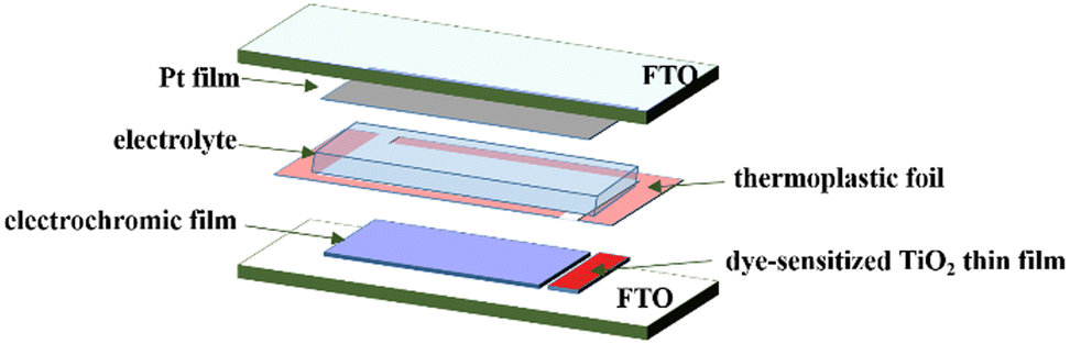 | ||
| Scheme 1 Configuration of PEC devices. | ||
Integration of photovoltaic thin films
A photovoltaic thin film was integrated into the aforementioned EC device to prepare a PEC device that was a self-driving device. The dye-sensitized TiO2 thin film was used as the photovoltaic film of the PEC device given that its working mode is compatible with that of the EC film. We prepared an EC thin film and the photovoltaic thin film on same electrode of the self-driving device (Scheme 1). Given that high-temperature heat treatment was required for the preparation of the dye-sensitized TiO2 films, they were prepared before forming the EC films to avoid the influence of heat treatment on the performance of the EC thin films. Moreover, the TiO2 photovoltaic film covered the smaller area of the electrode. The 20 nm particle-size TiO2 paste was coated via the doctor blade technique and its thickness was controlled using Scotch tape (3 M). The electrode coated with the TiO2 paste was gradually heated under an airflow at 325 °C for 5 min, 375 °C for 5 min, 450 °C for 15 min, and finally 500 °C for 15 min. Then, the as-prepared TiO2 films were immersed in a 0.5 mM N-719 dye solution in a mixture of acetonitrile and tertbutyl alcohol (volume ratio of 1:1) and kept at room temperature for 20–24 h to ensure the complete uptake of the sensitizer. After forming the dye-sensitized TiO2 films, the EC films were prepared through the process described above, and finally the PEC devices were obtained using the same assemblage process as that for the EC device.
Characterization
A field-emission scanning electron microscope (FE-SEM, Hitachi, Ltd, Tokyo, Japan) was used to study the surface morphology of the films. Their optical properties were measured using an ultraviolet-visible-near infrared spectrophotometer (UV-VIS-NIR, Lambda950, Perkin). X-ray diffraction (XRD) measurements were performed on a Bruker/D8 FOCUS X-ray diffractometer (Billerica, MA, USA) with a Cu Kα radiation source (wavelength of 1.5405 Å). Electrochemical performances were tested on an electrochemical workstation (Zahner, Germany). The current density–voltage (J–V) characterizations were carried out on a Keithley 2400 source meter under AM 1.5G simulated sunlight (100 mW cm−2).Results and discussion
Electrochromic films
The as-prepared WO3/TiO2 composite films were smooth and dense, as exhibited by the SEM image (Fig. S1a, ESI†), implying that the TiO2 thin film was stably and uniformly formed on the surface of the WO3 film. The XRD pattern of the WO3/TiO2 complex film revealed that the as-deposited WO3 film was amorphous, whereas the TiO2 film was too thin to display an XRD peak (Fig. S1b, ESI†).In the case of smart windows, EC films are usually required to be highly transparent in their original state. Thus, we measured the transmission spectra of the individual WO3 film and WO3/TiO2 complex films, as shown in Fig. 1(a). The transmittance of all the samples exceeded 90% for a wavelength greater than 417 nm in the visible light range. Moreover, compared with the WO3 film, the transmittance of WO3/TiO2 complex films showed a slight decrease and significant resonance peaks appeared in the spectrum at a wavelength greater than 600 nm. Our analysis showed that these resonance peaks were the result of the mutual enhancement between the interference of the WO3 film and that of the TiO2 film.
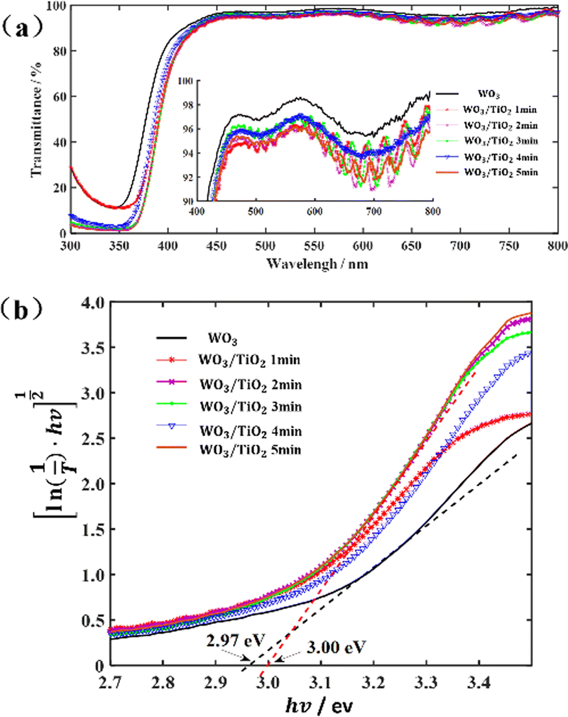 | ||
Fig. 1 (a) Transmittance spectra of the individual WO3 film and WO3/TiO2 complex films and (b) curve of 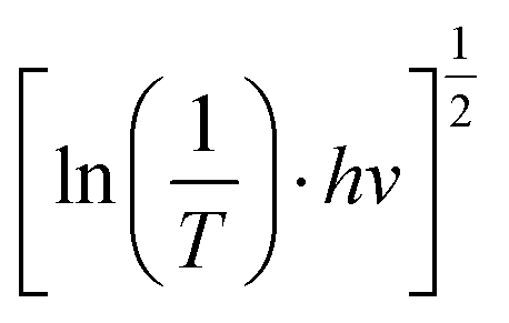 versus hv. versus hv. | ||
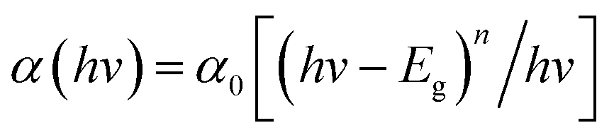
To clarify the effect of the TiO2 layer on the optical property of the EC film, we evaluated the bandgap (Eg) of the individual WO3 film and WO3/TiO2 complex films using Tauc's method, as follows:21
 | (1) |
 | (2) |
 | (3) |
 versus hv, the Eg of the samples was determined by extrapolating the linear least squares fit of
  to zero (Fig. 1b). Obviously, the Eg showed an increasing trend after the introduction of the TiO2 interface layer. The Eg of the WO3 film was 2.97 eV, whereas the Eg increased to 3.00 eV for WO3/TiO2_5 min.
Electrochromic devices
EC devices were packaged based on the EC films. In the experiment, we found that the a deposition time of more than 3 min for the TiO2 interface layer led to a decline in the bleaching-colouring performance of the device. Therefore, the samples based on the individual WO3 film, WO3/TiO2_1 min film, WO3/TiO2_2 min film, and WO3/TiO2_3 min film were mainly explored.For the proposed ECs, LixWO3 was generated in the WO3 film, thereby introducing the LixWO3 energy level in the WO3 energy band, which was reported to be slightly below the conduction band edge (EC) of WO3.23 This means that the localized state just below the EC of WO3 is a crucial parameter for exploring the bleaching-colouring performances. Herein, firstly, we investigated the effect of the TiO2 film on the electrochromic properties through the localized states of the individual WO3 film and WO3/TiO2 composite films.
The localized states below the conduction band (EC) or above the valence band (Ev) participate in light absorption, which can be represented by Urbach energy (EU), as shown below:24,25
 | ([4]) |
The absorption spectra of the WO3 film and WO3/TiO2 composite films in both the bleached and coloured states were measured to explore the changing trend of the localized states (EU) within their bandgap (Fig. S2a, ESI†). Fig. 2 shows the derived relationship between the function ln(A) and the variable hv, where A represents the absorbance. Replacing the absorption coefficient with the absorbance did not change the slope of the curve, and therefore it did not change the value of EU.
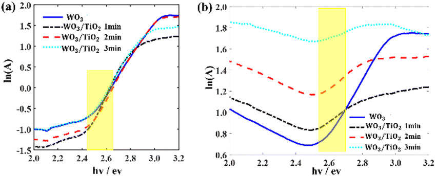 | ||
| Fig. 2 Relationship between the function ln(A) and variable hv from the absorption spectra (a) in the bleached state and (b) in the coloured state. EU was derived within the yellow range. | ||
For the EC devices based on WO3, WO3/TiO2_1 min, WO3/TiO2_2 min, and WO3/TiO2_3 min, the values of EU were 0.298 eV, 0.167 eV, 0.178 eV, and 0.189 eV when the devices were in the bleached state, whereas they increased to 0.384 eV, 0.892 eV, 1.158 eV, and 1.912 eV, respectively, when the devices were in the colouration state. We considered that the energy level of LixWO3 slightly below the EC of WO313 was the main contributor to the increase in EU when the device transitioned from the bleached state to coloured state. Interestingly, under the bleaching condition, the EU values of all the WO3/TiO2 composite films were smaller than that of the individual WO3 film, whereas under colouration condition, they exhibited a significant increase, even greatly exceeding the EU value of the coloured WO3. This indicates that the TiO2 interface layer reduced the amount of undesirable localized states by protecting WO3 from electrolyte corrosion and increased the amount of Li+ ions embedded in WO3 for device colouration. Undoubtedly, the positive effect of the TiO2 interface layer enlarged the optical transmission modulation range of the EC devices, which was confirmed by the transmission spectrum and cyclic voltammetry measurements.
The transmission spectra of the EC devices under a driving voltage of +0.6 V and −0.6 V indicated that the TiO2 surface layer increased the transmittance in the bleached state and reduced the transmittance in the coloured state, thereby increasing the transmission modulation range (Fig. 3a). Taking 600 nm as an example, the modulation range of the WO3/TiO2-based EC devices reached 73.9%, which was larger than that of 62.5% for the WO3-based EC devices. The bleaching time and coloration time of these EC devices were revealed by bleaching-colouring kinetic measurements (Fig. 3b). As a reference level to calculate the colouring time or the bleaching time of the device, the highest transmittance in the bleaching state as well as the lowest transmittance in the colouring state of the device were measured. The calculation range of the colouring time is the time it takes to decrease from the highest transmittance to 90% of the lowest transmittance. Similarly, the calculation range of the bleaching time is the time it takes to increase from the lowest transmittance to 90% of the highest transmittance. Obviously, the TiO2 interface layer hardly changed the time from bleaching to colouring, which was around 20 s, but it prolonged the time from colouring to bleaching, and the longer the sputtering deposition time of the TiO2 film, the longer the bleaching time of the device, from 12 s to 20 s. The cause for this phenomenon can be explained by the energy levels, as shown in Fig. 3(c).26 The Fermi levels of the WO3 film were represented by two dashed lines to consider the electrochromic state of the film, where Efb and Efc indicate the Fermi level in the bleached and coloured state, respectively.27 The relative position of the Fermi level in the coloured WO3 with respect to the Fermi level of TiO2 plays a pivotal role in determining the responsivity of the bleaching process.26 When the Efc of the coloured WO3 is higher than or close to the Ef of TiO2, electrons would transfer to the TiO2 film and be trapped there, resulting in an extension of the bleaching time of the device.
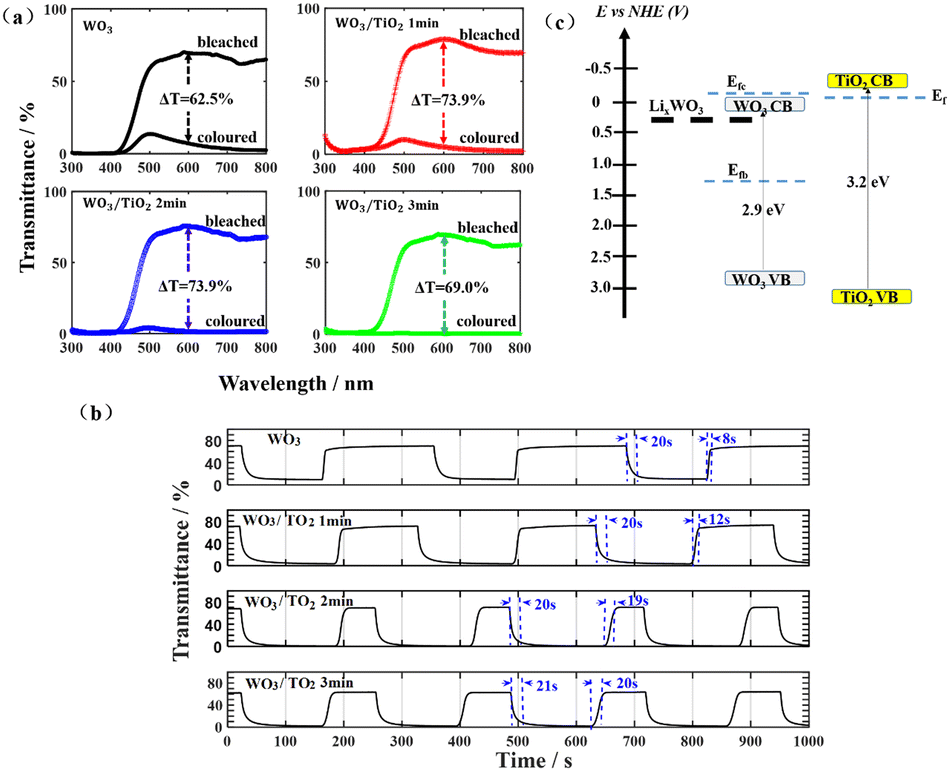 | ||
| Fig. 3 (a) Transmittance spectra of these EC devices based on the WO3 film and WO3/TiO2 composite films. (b) Bleaching-colouring kinetic measurements at the wavelength of 600 nm under alternating voltaic cycles from −0.6 V to 0.6 V and (c) energy level diagrams for WO3, TiO2 and LixWO3. | ||
The impact of the TiO2 interface layer on the electrochromic performance was further explored though cyclic voltammetry (CV) measurements, as shown in Fig. 4(a). By careful observation, it was observed that for the WO3 film, both the anodic current peak and cathodic current peak were located at −0.097 V. However, upon the introduction of a TiO2 layer on the WO3 surface, the anodic peaks shifted towards a positive voltage, while the cathodic peak deviated to a negative voltage. This phenomenon has also been found in a TiO2 nanotube material decorated with WO3 particles and WO3–TiO2 core–shell nanowires, which was considered to be the synergistic effect of these two materials.28,29
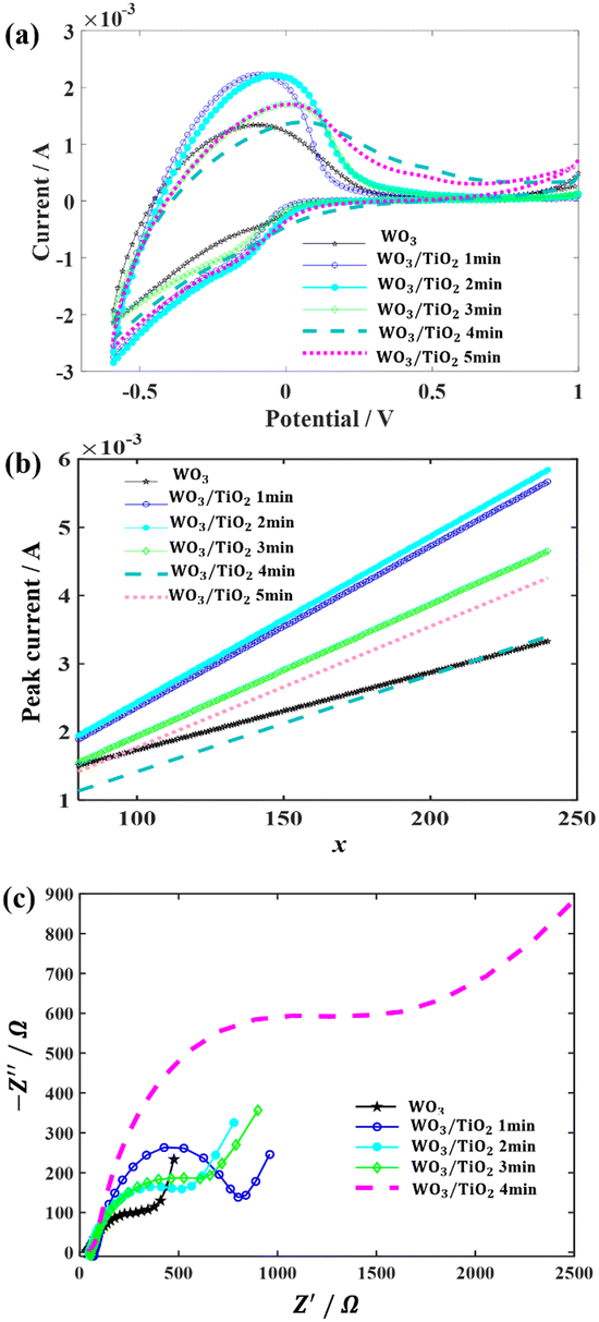 | ||
| Fig. 4 (a) Cyclic voltammograms between −0.6 V and 1.0 V at a voltaic scan rate of 10 mV s−1 for the devices based on the individual WO3 film and WO3/TiO2 composite films. (b) Linear fitting of the peak currents (IP) and the variables x = 2.71 × 10⁵ × S × n3/2 × D1/2 × C0 × v1/2 at the scan rate (v) of 10 mV s−1, 30 mV s−1, 50 mV s−1 and 100 mV s−1. (c) Comparison of the impedance spectra of the devices. The effective area of all the devices was 2.0 cm2. | ||
The inserted charge density (Qc) and extracted charge density (Qb) were recorded by CV measurements, and based on the Qcs, the coloured efficiencies (CE) of the devices were derived. These physical parameters are summarized in Table 1. Compared with the WO3-based EC device, the introduction of a TiO2 interface layer significantly increased the inserted charge density and the extracted charge density. Furthermore, there was a remarkable decrease in the difference between the inserted charge density and the extracted charge density, indicating the improvement effect of the TiO2 interface layers on the cycle stability of the devices. Combined with the previous analysis of the EU, we believe that the surface of WO3 was passivated by TiO2, and thus its surface state was not subject to electrolyte corrosion, which hindered the generation of irreversible localized states.
| Sample name | Q c/Qb (C) | Q b/Qc (%) | CE at wavelength of 600 nm (cm2 C−1) | D (cm2 s−1) |
|---|---|---|---|---|
a
Q
c or Qb was obtained in accordance with the CV measurements by the formula 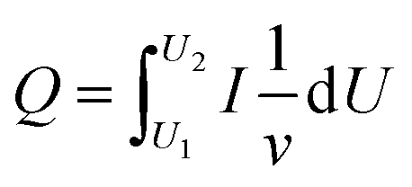 , where v represents the potential scan rate.
b CE was obtained from the formula , where v represents the potential scan rate.
b CE was obtained from the formula 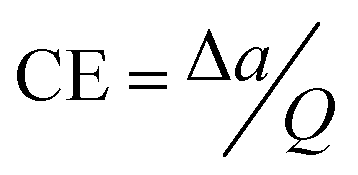 , where Δa stands for the optical absorption difference between the coloration state and bleached state. , where Δa stands for the optical absorption difference between the coloration state and bleached state.
|
||||
| WO3 | 0.0739/0.0669 | 90.5 | 31 | 2.1668 × 10⁻¹⁰ |
| WO3/TO2 1 min | 0.1000/0.0977 | 97.9 | 28 | 5.5790 × 10⁻¹⁰ |
| WO3/TO2 2 min | 0.1113/0.1066 | 95.8 | 35 | 5.9195 × 10⁻¹⁰ |
| WO3/TO2 3 min | 0.0860/0.0816 | 94.9 | 69 | 3.7520 × 10⁻¹⁰ |
| WO3/TO2 4 min | 0.1041/0.0889 | 85.4 | — | 2.0079 × 10⁻¹⁰ |
| WO3/TO2 5 min | 0.1062/0.0981 | 92.3 | — | 3.1471 × 10⁻¹⁰ |
In accordance with the optical absorption measurements and the derived charge density, the coloured efficiencies of the devices were calculated, as listed in Table 1. There are many physical variables that affect the colouring efficiency, including film thickness, material properties, and driving charge density, and thus it is a multivariable function. In our experiments, the devices based on the WO3/TiO2_3 min film had a high coloration efficiency (CE) of about 69 cm2 C−1.
In addition, based on the CV curves, the diffusion coefficient, D (cm2 s−1), of Li+ was calculated using the peak current, IP, during the anode scans at different scanning rates, as follows:20
| IP = 2.71 × 10⁵ × S × n3/2 × D1/2 × C0 × v1/2 | (5) |
Subsequently, 1000 repeated CV measurements were conducted on the WO3 device and the WO3/TiO2_2 min device to investigate the effect of the TiO2 interface layer on the device lifetime. Fig. 5a demonstrates that the closed area of the CV curve of the WO3/TiO2_2 min device was remarkably larger than that of the WO3 device, and furthermore Fig. 5b obviously shows that the difference between the inserted and extracted charge density of the WO3/TiO2_2 min device was smaller than that of the WO3 device. Thus, these results indicate that a TiO2 interface layer with an appropriate thickness is greatly beneficial for improving the lifespan of EC devices.
 | ||
| Fig. 5 (a) Cyclic voltammograms for 1000 cycles over the potential range of −0.6 V to 1.0 V at a scan rate of 100 mV s−1 for the WO3/TiO2_2 min device and WO3 device. (b) Difference between the inserted and extracted charge density of the WO3/TiO2_2 min device and WO3 device during 1000 CV cycles. The effective area of all the devices was 2.0 cm2. | ||
Photoelectrochromic devices
We integrated a dye-sensitized TiO2 thin film into the EC device and constructed a PEC device (Scheme 1). The dye-sensitized TiO2 thin film, together with the electrolyte and the electrode shared by the EC device formed a photovoltaic cell. Under illumination, the charges generated by the photovoltaic cell directly drove the electrochromic film to change color, and the driving mechanism has been reported in the literature.30 This driving process avoids energy loss at the joints and in wires when connecting wires externally, and therefore PEC devices can change color sufficiently at a low self-driving energy. To prove this, we investigated the photoelectric conversion efficiency and the electrochromic property of the PEC devices.The self-driving energy of the PEC device was shown by current density–voltage (J–V) measurements (Fig. 6a). The photoelectric conversion efficiency of the PEC device was very low, i.e., only 1.19%, whereas its fill factor (FF) was high, which indicated that the dye-sensitized TiO2 thin film possessed a high capacity for doing work.
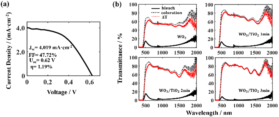 | ||
| Fig. 6 (a) Current density–voltage (J–V) characterization of the PEC device. (b) Transmittance spectra of these PEC devices based on the WO3 film and WO3/TiO2 composite films, whose transmittance was driven by the dye-sensitized TiO2 film. | ||
The variation in the transmittance spectrum of the PEC devices under self-driving energy was investigated in a wide electromagnetic wave range of 400 nm to 2000 nm, as shown in Fig. 6(b). All the tested devices exhibited a high transmission modulation range under very low self-driving energy. In addition, it can be seen that the TiO2 interface layer increased the transmittance of the PEC devices in the bleached state and enhanced the absorbance of the devices in the coloured state, thereby significantly enlarging the transmission modulation range. Especially for the PEC device based on the WO3/TiO2_3 min composite film, the transmission modulation range ΔT exceeded 80% in the wavelength range of 545 nm to 1077 nm. Simultaneously, the coloured PEC device based on the WO3/TiO2 film had extremely low transmittance in the near-infrared range, which indicates that this device has promising application prospects in smart windows and heat insulation layers.
Photos of the EC device and PEC device in the initial sate, coloured state and bleached state are shown in Fig. S4 and S5 (ESI†), respectively. To elucidate the advantages of the as-prepared devices, we compared their electrochromic properties with that of various TiO2/WO3 composite thin films prepared by representative techniques over the past decade, as listed in Table 2. It is worth noting that due to the lack of research reports on packaged EC or PEC devices based on TiO2/WO3 films, the electrochromic properties of the TiO2/WO3 films listed in Table 2 were all obtained using electrochemical cells with three electrodes.
| Preparation method | T b –Tc (%) | Coloration time | CE (cm2 C−1) | Cycling stability | Production scale | Ref. | |
|---|---|---|---|---|---|---|---|
| WO3/TiO2 core/shell nanowires | The method of template and sputtering | 41.8/650 nm | 30 s | 41.6/650 nm | Peak current decreased after 10 cycles | Poor | 31 |
| 72.8/950 nm | 67.4/950 nm | ||||||
| WO3/TiO2 Honey-comb films | Anodizing co-sputtered W/Ti films | 57.6/550 nm | 41 s 550 nm | 21.8/550 nm | ΔT did not decrease after 500 cycles | Poor | 32 |
| 71.5/633 nm | 38 s 633 nm | 35.2/633 nm | |||||
| 68.7/800 nm | 24 s 800 nm | 63.8/800 nm | |||||
| TiO2/WO3 core/shell nanoarrays | Hydrothermal method and sol–gel route | 16–73 | — | — | Peak current decreased after 300 cycles | Poor | 33 |
| TiO2/WO3 inverse opal structure films | The method of template and dip-coating | 65/1033 nm | 6 s 1033 nm | 111.9/1033 nm | Sustain 90% of the original contrast after 1200 cycles | Poor | 19 |
| TiO2 on WO3 nanowire arrays | Hydrothermal method and magnetron sputtering | 87.0/1500 nm | 3 s 633 nm | 102.1/633 nm | 95.6% after 3000 cycles | Poor | 12 |
| 85.3/633 nm | |||||||
| WO3/TiO2 films | A co-solvent method and spin coating method | 62.8/633 nm | 3.3 s | 57.2/633 nm | The peak current ratio compared with the first cycle are ∼80% after CV 1000 cycles | Poor | 18 |
| Hierarchical structure WO3/TiO2 films | radio frequency magnetron sputtering | 80/500–900 nm | 30 s | — | Oxidation peak current was no significant change after 1000 cycles | Excellent | 20 |
| TiO2-doped WO3 films | DC reactive magnetron sputtering | Low | 0.55 s | 581.39 | — | Excellent | 34 |
| Devices based on WO3/TiO2 films | DC reactive magnetron sputtering | >80% 545–1077 nm | 21 s/600 nm | 69/600 nm | Reversibility was no significant change after 1000 cycles | Excellent | This work |
Summary
A comprehensive investigation into the electrochromic properties of WO3/TiO2-based devices was reported herein. Based on several experiments, the optimal sputtering time range for the TiO2 interface layer was discovered. The TiO2 interface layer prepared with a sputtering time of 2–3 min was capable of enhancing the electrochromic properties of the WO2-based devices significantly. When the TiO2 sputtering time was less than 2 min, the device performance was not significantly improved, while when the TiO2 sputtering time was greater than 3 min, the device performance deteriorated, which was manifested as a prolonged response time, and even the inability to change color under a small voltage.Compared with the WO3-based EC devices, the EC devices based on the optimized WO3/TiO2 film possessed a larger transmission modulation range, higher CE value, superior cyclic stability. Specifically, the WO3/TiO2_2 min-based EC device was capable of thoroughly bleaching or colouring driven by a low voltage of 0.6 V, and the bleaching time and the colouring time were 19 s and 20 s, respectively. After 1000 CV measurements, the reversibility of the device had almost no attenuation, as reflected in the extremely small difference between the inserted charge density and the extracted charge density. Driven by the dye-sensitized TiO2 film, the PEC device based on the optimized WO3/TiO2 composite film exhibited a high transmittance in the electromagnetic wavelength range of 500 nm to 1800 nm under the bleaching condition, whereas it had a large absorbance under the colouring condition. Obviously, it possessed a large transmission modulation range, where especially that in the range of 545 nm to 1077 nm exceeded 80%.
Through the quantitative analysis of important physical quantities such as the bandgap (Eg), localized state (EU), driving charge density, and electrochromic performance, we investigated the mechanism of the TiO2 interface layer affecting the electrochromic performance of the EC devices. The TiO2 interface layer significantly reduced irreversible localization states on the WO3 surface and obviously increased the ion density driving the bleaching-colouring process. These are the main reasons why TiO2 improved the transmission spectra, transmission modulation range and reversible stability of the EC and PEC devices.
Author contributions
Panshu Gui and Ziyi Jin contributed equally to this work. Panshu Gui fabricated the devices and Ziyi Jin conducted the photoelectrochemical performance measurements. Yufeng Bai, Zhengqiao Lv, and Jianwei Mo measured the electrochromic performance of devices. Di Yang wrote the manuscript. The authors thank Prof. Shuai Chang from Shenzhen MSU-BIT University for discussion of the device operational mechanism.Conflicts of interest
The authors declare no competing financial interest.Acknowledgements
This work was supported by the National Nature Science Foundation of China (22173009, 22211530439).References
- C. Bechinger, S. Ferrere, A. Zaban, J. Sprague and B. A. Gregg, Photoelectrochromic windows and displays, Nature, 1996, 383(6601), 608–610 CrossRef CAS.
- S. Bogati, A. Georg and W. Graf, Photoelectrochromic devices based on sputtered WO3 and TiO2 films, Sol. Energy Mater. Sol. Cells, 2017, 163, 170–177 CrossRef CAS.
- K. Tang, Y. Shi, Y. D. Cui, J. Shu, X. Wang, Y. Qin, Y. Liu, J. Tan, H. HoeWu and Y. Cheng, Fabrication of WO3/TiO2 core-shell nanowire arrays: Structure design and high electrochromic performance, Electrochim. Acta, 2020, 330 Search PubMed.
- R.-T. Wen, C. G. Granqvist and G. A. Niklasson, Eliminating degradation and uncovering ion-trapping dynamics in electrochromic WO3 thin films, Nat. Mater., 2015, 14(10), 996–1001 CrossRef CAS PubMed.
- K.-W. Kim, T. Y. Yun, S.-H. You, X. Tang, J. Lee, Y. Seo, Y.-T. Kim, S. H. Kim, H. C. Moon and J. K. Kim, Extremely fast electrochromic supercapacitors based on mesoporous WO3 prepared by an evaporation-induced self-assembly, NPG Asia Mater., 2020, 12(1), 84 CrossRef CAS.
- P. K. Shen, K. Y. Chen and A. C. C. Tseung, Electrochromism of electrodeposited tungsten trioxide films; 1: Electrochemical characterization, J. Electrochem. Soc., 1994, 141(7), 1758 CrossRef CAS.
- K. Tang, Y. Zhang, Y. Shi, J. Cui and Y. Wu, Crystalline WO3 nanowires array sheathed with sputtered amorphous shells for enhanced electrochromic performance, Appl. Surf. Sci., 2019, 498, 143796 CrossRef CAS.
- X. Li, T. YongKim, K.-W. Kim, S. HyunMoon and H. Chul, Voltage-Tunable Dual Image of Electrostatic Force-Assisted Dispensing Printed, Tungsten Trioxide-Based Electrochromic Devices with a Symmetric Configuration, ACS Appl. Mater. Interfaces, 2020, 12(3), 4022–4030 CrossRef CAS PubMed.
- D. Dong, J. Robichaud and Y. Djaoued, Colorimetric Properties and Structural Evolution of Cathodic Electrochromic WO3 Thin Films, Can. J. Chem., 2021, 99(6), 549–556 CrossRef CAS.
- Y. Yao, Q. Zhao, W. Wei, Z. Chen and Y. Gao, WO3 Quantum-dots Electrochromism, Nano Energy, 2019, 68, 104350 CrossRef.
- M. A. A, Y. E. F. B, S. R. T. A and A. P. A, Fast electrochromic response and high coloration efficiency of Al-doped WO3 thin films for smart window applications, Ceram. Int., 2021, 47(23), 32570–32578 CrossRef.
- J. Feng, X. Zhao, B. Zhang, Z. Chen, Z. Li and Y. Huang, In situ optical spectroscopic understanding of electrochemical passivation mechanism on sol–gel processed WO3 photoanodes, J. Energy Chem., 2022, 71, 20–28 CrossRef CAS.
- M. P. Rodrigues, C. M. Cholant, L. U. Krüger, L. M. Rodrigues and C. O. Avellaneda, A Diffusional Study of Electrochromical Effect and Electrointercalation of Li+ Ions in WO3 Thin Films, J. Electron. Mater., 2021, 50(3), 1207–1220 CrossRef CAS.
- Y. Cui, Q. Wang, G. Yang and Y. Gao, Electronic properties, optical properties and diffusion behavior of WO3 with H+, Li+ and Na+ intercalated ions: A first-principles study, J. Solid State Chem., 2021, 297(S1), 122082 CrossRef CAS.
- A. Dokouzis, D. Zoi and G. Leftheriotis, Photoelectrochromic Devices with Enhanced Power Conversion Efficiency, Materials, 2020, 13(11), 2565 CrossRef CAS PubMed.
- Z. Wang and X. Hu, Electrochromic properties of TiO2-doped WO3 films spin-coated from Ti-stabilized peroxotungstic acid, Electrochim. Acta, 2001, 46(13–14), 1951–1956 CrossRef CAS.
- A. Park, Development of WO3 thin films using nanoscale silicon particles, Jpn. J. Appl. Phys., 2000, 39, 3572–3578 CrossRef.
- C. Hua, G. Yuan, Z. Cheng, H. Jiang, G. Xu, Y. Liu and G. Han, Building architecture of TiO2 nanocrystals embedded in amorphous WO3 films with improved electrochromic properties, Electrochim. Acta, 2019,(309), 354–361 CrossRef CAS.
- H. Ling, L. P. Yeo, Z. Wang, X. Li, D. Mandler, S. Magdassi and A. I. Y. Tok, TiO2–WO3 core–shell inverse opal structure with enhanced electrochromic performance in NIR region, J. Mater. Chem. C, 2018, 6 Search PubMed.
- H. N. Wang, Hierarchical structure WO3/TiO2 complex film with enhanced electrochromic performance, Solid State Ionics, 2019, 338, 168–176 CrossRef.
- J. Ruska, Amorphous and Liquid Semiconductors, Proceedings of the Fifth International Conference, Garmisch-Partenkirchen, Taylor and Francis Ltd, London, 1974, p. 779 Search PubMed.
- A. R. Zanatta, Revisiting the optical bandgap of semiconductors and the proposal of a unified methodology to its determination, Sci. Rep., 2019, 11225 CrossRef CAS PubMed.
- G. Syrrokostas, A. Dokouzis, S. N. Yannopoulos and G. Leftheriotis, Novel photoelectrochromic devices incorporating carbon-based perovskite solar cells, Nano Energy, 2020, 105243 CrossRef CAS.
- F. Urbach, The Long-Wavelength Edge of Photographic Sensitivity and of the Electronic Absorption of Solids, Phys. Rev., 1953, 92(5), 1324 CrossRef CAS.
- H. Lee, Y. T. Huang, M. W. Horn and S. P. Feng, Engineered optical and electrical performance of rf–sputtered undoped nickel oxide thin films for inverted perovskite solar cells, Sci. Rep., 2018, 8(1), 5590 CrossRef PubMed.
- A. Cannavale, M. Manca, F. Malara, L. D. Marco, R. Cingolani and G. Gigli, Highly efficient smart photovoltachromic devices with tailored electrolyte composition, Energy Environ. Sci., 2011, 4(7), 2567–2574 RSC.
- A. Azens and C. Granqvist, Electrochromic smart windows: energy efficiency and device aspects, J. Solid State Electrochem., 2003, 7(2), 64–68 CrossRef CAS.
- N. M. Vuong, D. Kim and H. Kim, Electrochromic properties of porous WO3–TiO2 core–shell nanowires, J. Mater. Chem. C, 2013, 1(21), 3399–3407 RSC.
- Y. Y. Song, Z. D. Cao, J. H. Wang, X. H. Xia and R. Lynch, Multistage Coloring Electrochromic Device Based on TiO2 Nanotube Arrays Modified with WO3 Nanoparticles, Adv. Funct. Mater., 2011, 21(10), 1941–1946 CrossRef CAS.
- A. Dokouzis, D. Zoi and G. Leftheriotis, Photoelectrochromic Devices with Enhanced Power Conversion Efficiency, Materials, 2020, 13(11), 2565 CrossRef CAS PubMed.
- N. M. Vuong, D. Kim and H. Kim, Electrochromic properties of porous WO3-TiO2 core-shell nanowires, J. Mater. Chem. C, 2013, 1(21), 3399–3407 RSC.
- Y. Gui and D. J. Blackwood, Honey-Comb Structured WO/TiOThin Films with Improved Electrochromic Properties. 2015.
- Y. Li, Z. Liu, L. Zhou, T. Cui, B. Wang, K. Guo and J. Han, Titanium dioxide/tungsten trioxide nanoarrays film for high electrochromic performance, Electrochim. Acta, 2015, 173, 117–123 CrossRef CAS.
- K. Rao, V. C. Babu, V. R. Kumar and N. Veeraiah, Characterization and coloration efficiency studies using cyclicvoltammetry and chronocoulometric methods on TiO2 doped WO3 nanocrystalline thin films, Optik, 2022, 249, 168282 CrossRef.
Footnotes |
| † Electronic supplementary information (ESI) available. See DOI: https://doi.org/10.1039/d3ma00272a |
| ‡ Equal contribution. |
| This journal is © The Royal Society of Chemistry 2023 |