
 Open Access Article
 This Open Access Article is licensed under a Creative Commons Attribution-Non Commercial 3.0 Unported Licence
The modulation of the electrical and optical properties of Cs2TiBr6 by doping
Jianwei
Wei
 *a,
Junhua
Wu
a,
Yunyun
Wang
a,
Yuze
Zhang
a,
Zengwei
Ma
a,
Chenkai
Qiao
a and
Hui
Zeng
ab
*a,
Junhua
Wu
a,
Yunyun
Wang
a,
Yuze
Zhang
a,
Zengwei
Ma
a,
Chenkai
Qiao
a and
Hui
Zeng
ab
aScience of College, Chongqing University of Technology, 400054, Chongqing, China. E-mail: redskywei@cqut.edu.cn
bSchool of Electronic and Optical Engineering, Nanjing University of Technology, 210094, Nanjing, China
First published on 28th July 2023
Abstract
As one of the most promising light absorbing-materials, all inorganic lead-free perovskite Cs2TiBr6 has obvious advantages, such as outstanding photoelectric properties, an adjustable band gap, and environmental friendliness. However, the wide band gap limits its application in optoelectronic devices. Here, the modulation of its electrical and optical properties by doping is investigated based on first-principles density functional theory (DFT). The elements Si, Ge, and Te are used to substitute Ti, and Br is substituted by Cl and I with different concentrations, respectively. Compared with the pristine material, Cs2Ti0.5Ge0.5Br6 has better physical stability, and a smaller band gap (1.33 eV). The light absorption is broadened obviously because of the states of 4s from Ge. Similarly, the band gap of Cs2Ti(Br0.75I0.25)6 is 1.29 eV and its visible light absorption was enhanced due to the 5p electron of the I atom. Furthermore, the quasi-direct band gap of the original material is adjusted to the direct band gap, which approaches the optimum band gap. Our results indicate that doping modulation will greatly improve the prospects of the Cs2TiBr6 perovskite for application in solar cells.
1. Introduction
Solar energy has attracted more and more attention due to easy access and environmental protection.1–3 In the past decade, perovskite solar cells (PSCs) with low cost and easy fabrication have been developed rapidly.4,5 The manufacturing technology has been improved continuously, and the photoelectric conversion efficiency (PCE) has jumped from 3.8%6 in 2009 to 23.7%7 in 2019. However, a large number of toxic elements lead and organic cations with insufficient environmental tolerance are considered to be the main factors preventing their commercialization.8 Therefore, lead is replaced with other non-toxic or less toxic and environment-friendly transition metals, such as Sn, Bi, Sb, and Ti, to solve the toxicity problem.9,10 Replacing organic cations with cesium (Cs+) is a direction to solve the instability problem.11,12As a lead-free perovskite, Cs2TiBr6 shows strong adaptability under continuous sunlight or in humid environments due to the stable oxidation state of Ti atoms. In 2018, Ju et al.13 synthesized a Cs2TiBr6 perovskite material with a measured band gap value of 1.8 eV, and its energy band structure has a quasi-direct band gap because its band valleys at the Γ and X points were very close. In the same year, Chen et al.14 applied the material as the solar light absorption layer for the first time. The unpackaged cell still maintained 90% of the original efficiency under the conditions of a temperature of 70 °C, a humidity of 30% and ambient light irradiation for 350 h. The equilibrium carrier diffusion length was >100 nm, but the initial PCE was only 3.28%. It is proved that although the material has excellent stability, it has a disadvantage of low PCE. To improve the application value of the material in the photovoltaic field, Li et al.15 doped it with Cl and I. The results show that Cl doping at 25% concentration results a suitable band gap and enhances the stability of the system. Lu et al.16 studied a Si and Cl co-doped Cs2TiBr6 system by using the combination of non-adiabatic molecular dynamics (NAMD) and time-domain density functional theory (TD-DFT). The results show that doping avoids deep defects and inhibits electron hole recombination. It can be seen that doping is helpful to improve the photoelectric properties of Cs2TiBr6.
Herein, the Cs2TiBr6 material has been studied carefully using the first-principles method in many aspects. This work is the first comprehensive study to show that the electrical and optical properties of Cs2TiBr6 can be modulated by doping. It has been proved that doping with semi-metallic elements improves the photoelectric properties of perovskite materials.17–19 Besides, several teams20–24 pointed out that Cl doping is helpful to strengthen the stability of perovskite. However, there is no systematic and accurate description of the mechanism of doping effects. In this work, the physical stability and electrical properties of the Cs2TiBr6 material doped with different concentrations of semi-metallic elements Si, Ge, and Te, and halogen elements were studied. In order to obtain more accurate results, the GGA + U method25 is employed for the calculations. This work not only overcomes the shortcomings of previous studies on the halogen-doped Cs2TiBr6 system but also investigates the doping effects of the Ti atom substitution by semi-metallic elements. Therefore, this work provides a significant guidance to develop and design high-performance all-inorganic lead-free perovskites.
2. Methods and models
First-principles simulations are performed using the VASP software package26,27 based on DFT. The wave function is expanded by the projected augmented plane wave method, and the exchange correlation interaction is treated by generalized gradient approximation (GGA) in the Perdew–Burke–Ernzerhof (PBE) method. The energy cutoff value is set to 520 eV, the force convergence standard is set to 0.01 eV Å−1, and the energy convergence standard of self-consistent field (SCF) iteration is set to 10−6 eV. 8 × 8 × 8 k-point meshes are selected for the calculations. The strongly correlated electrons in Ti-3d orbitals are modified using the Hubbard U model.28–30 VASPKIT is used to process the calculated data,31 VESTA software is used to visually display the crystal structure, and LOBSTER software is used to calculate the crystal orbital Hamiltonian layout between two atoms.32–34 The Cs2TiBr6 model consists of 36 atoms with a space group of Fm![[3 with combining macron]](https://www.rsc.org/images/entities/char_0033_0304.gif) m. We have established 17 doping structures for halogen and semi-metallic doping. The doping positions are shown in Fig. 1.
m. We have established 17 doping structures for halogen and semi-metallic doping. The doping positions are shown in Fig. 1.
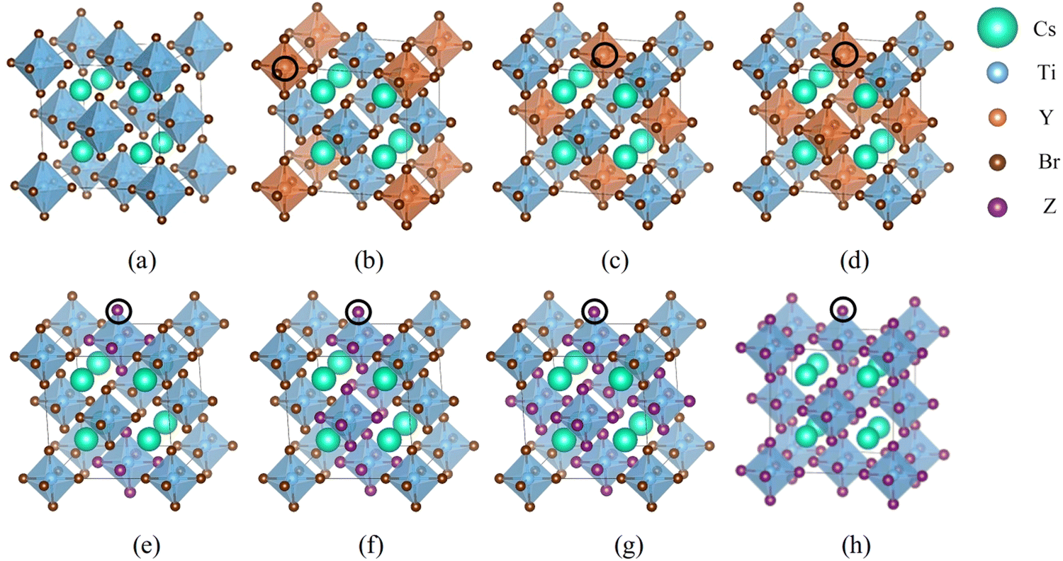 | ||
| Fig. 1 Schematic diagrams of structures and doping positions. (a) The pristine Cs2TiBr6. (b)–(d) The semi-metallic doping models Cs2Ti1−xYxBr6 (Y = Si, Ge and Te) with x = 0.25, 0.5 and 0.75, respectively. The doping atoms are represented by orange balls located at the every center of orange octahedron. The locations are marked by black circles. (e)–(h) are halogen doping Cs2Ti(Br1−xZx)6 (Z = Cl, I) with x = 0.25, 0.5, 0.75 and 1, respectively. The doping atoms are represented by purple balls located at the octahedron vertex. The locations are marked by black circles. From (e) to (h) the doped octahedron increased from 1 to 4 in the supercell. | ||
3. Results and discussion
3.1 Geometry
After full relaxation for every structure, the lattice parameters of Cs2TiCl6, Cs2TiBr6, and Cs2TiI6 are 10.624 Å, 11.079 Å, and 11.878 Å, which are very close to the experimental values of 10.24 Å,35 10.92 Å13 and 11.67 Å,13 respectively. To analyze the physical stability of doping systems, the formation energy required for doping is calculated. The formation energy calculation formula is shown in eqn (1) and (2):36| ΔE = Etot[X] − Etot[Cs2TiBr6] + nBrμBr − nxμx | (1) |
| ΔE = Etot[X] − Etot[Cs2TiBr6] + nTiμTi − nyμy | (2) |
 | ||
| Fig. 2 Formation energies of different doping systems. | ||
As shown in Fig. 2, the formation energy of Cl doping is negative, and those of I, Si, Ge, and Te doping are positive. It shows that it is easier to replace Cl with Br than the other elements. With the increase of doping concentration, the additional energy required for I to replace Br and the additional energies required for Si, Ge, and Te to replace Ti gradually increase. Thus, high concentration doping is not conducive to experimental preparation.
3.2 Electrical properties
In order to better explore the influence of doping on the electronic structure of Cs2TiBr6, the energy band and density of states of the doped structures were further analyzed. The Fermi levels in the energy band structures have been set to zero. Fig. 3(a) shows the energy band structure of the Cs2TiBr6 cell. Actually, the band gap of Cs2TiBr6 is an indirect gap, which is called the quasi-direct band gap for the primitive cell. But the selected crystal cell having 36 atoms is 4 times of primitive one. So the gap looked like a direct band gap because of the band folding of the Brillouin zone in the supercell. Its band shape and band gap width are very consistent with those in the literature.35 As shown in Fig. 3(b)–(d), the energy band structure of the system changes significantly after Ge doping. Ge doping results in an obvious impurity band in the forbidden band of the pristine system. The impurity band is contributed by Ge and Br, and its energy is lower than that of the impurity band contributed by the original system, becoming a new conduction band bottom. The impurity bands generated by Ge doping are close to the conduction band and the impurity band is a shallow impurity state. The shallow impurity level is conducive to the separation of optically excited electron hole pairs, and inhibits the recombination of optically excited carriers. For the 50% and 75% doping, the bottom curvature of the newly formed conduction band is significantly greater than that of the original system, which leads to the effective mass of electrons being less than that of the original system. The curvature in the valence band is basically unchanged. The band gap width of the 50% concentration is 1.33 eV, which evenly matches the optimum value.37 | ||
| Fig. 3 Schematic diagrams of energy band structures. (a) Band structure of Cs2TiBr6. (b)–(d) show Cs2Ti1−xGexBr6 (x = 0.25, 0.5 and 0.75), respectively. (e)–(h) Cs2Ti(Br1−xIx)6 (x = 0.25, 0.5, 0.75 and 1), respectively. | ||
Fig. 3(e)–(h) are schematic diagrams of the I doping energy bands. When I is doped, it directly replaces Br to form a new valence band top, and the conduction band bottom is contributed by I, Br, and Ti. With the increase of the concentration of the I atom, more and more energy subbands from I atom appear between the conduction band bottom and the valence band top of the pristine one. Therefore, the overall valence band is gradually raised and the band gap is decreased. This means a wider carrier diffusion length and better conductivity and better photoelectric conversion efficiency, compared with the pristine one. All doped structures are evaluated in terms of the energy band type and band gap value. When I is doped at 25%, the band gap of 1.29 eV is close to the S–Q theoretical37 limit band gap of 1.34 eV. So that Cs2Ti0.5Ge0.5Br6 and Cs2Ti(Br0.75I0.25)6 can be expected as the optimal materials for solar cells.
In order to understand the change of band gaps in detail, the partial density of states (PDOS) of each doped structure is calculated for different orbits of the corresponding elements. As shown in Fig. 4(a), we can find that the band gap width of Cs2TiBr6 is mainly determined by the energy position of Ti-3d and Br-4p. The upper valence band is mainly contributed by the Br-4p orbital of elements because of its high electronegativity and the lower valence band is formed by the hybridization of the Ti-3d orbital and Br-4p orbital. The conduction band is formed by the hybridization of Ti-3d and Br-4p orbitals.
 | ||
| Fig. 4 Schematic diagrams of density of states. (a) Cs2TiBr6. (b)–(d) Cs2Ti1−xGexBr6 (x = 0.25, 0.5, and 0.75), respectively. (e)–(h) Cs2Ti(Br1−xIx)6 (x = 0.25, 0.5, 0.75 and 1), respectively. | ||
The Ge doping introduces Ge-4p state electrons into the upper and lower valence bands, respectively, as shown in Fig. 4(b)–(d). From −1.5 eV to 0 eV, the states in the valence band mainly come from the Ge-4p and Br-4p states, which expand the valence band bandwidth. The impurity energy level generated by the hybridization of Ge-4s and Br-4p electrons appears in the band gap, forming a new conduction band bottom due to the energy of the Ge-4s orbital being lower than that of the Ti-3d orbital. When valence band electrons absorb photons, the transition to the impurity level is more energetic for the low-energy photons, around 1.5 eV. With the increase of the Ge concentration, the impurity band is extended and the band gap decreases. However, the band gap of Cs2Ti0.25Ge0.75Br6 is smaller than the S–Q limit. This indicates that increasing the Ge concentration is not a linearly effective method to the application in the photovoltaic cells.
In Fig. 4(e)–(h), the proportion of I-5p increases with the I concentration. The valence band is gradually occupied by the electron of I-5p, which results in the valence band moving to the higher region. The conduction band shifts to a low energy level, so the band gap decreases gradually. In the conduction band of the Cs2Ti(Br1−xIx)6 system, the energy level of the Ti atom's electronegativity is smaller than that of I atoms. Therefore, the conduction band of the doped structure is mainly formed by the mixed states of the Ti-3d, Br-4p, and I-5p electrons.
3.3 Optical properties
The doping elements cause the change of the energy band structure, which certainly could affect the optical properties of Cs2TiBr6 obviously. The optical properties of solids are represented by dielectric functions:| ε(ω) = ε1(ω) + iε2(ε) | (3) |
 | (4) |
 | (5) |
 | (6) |
 | ||
| Fig. 5 Optical absorption lines. (a) Cs2Ti1−xGexBr6 (x = 0.25, 0.5 and 0.75). (b) Cs2Ti(Br1−xIx)6 (x = 0.25, 0.5, 0.75 and 1). | ||
Three semi-metallic elements Si, Ge, and Te have been used to substitute Ti in Cs2TiBr6. But Ge is the only one that could expand the absorption spectrum obviously. As shown in Fig. 5(a), in the range of 300–594 nm, the light absorption capacity is almost reduced in equal proportion due to the doping of the Ge element. The Ge-4s orbital is incorporated into the original conduction band and Ti-3d orbital composition is reduced. The electrons of Ge-4p and Br-4p states in the valence band undergo p–s transition and the poor degeneracy of the s orbital is much less than that of d orbital of Ti. Thus, the electron transition intensity is small. With the increase of doping concentration, the impurity band formed by the hybridization of the Ge-4s orbital and Br-4p orbital reduces the band gap and improves the light absorption capacity with a wavelength greater than 545 nm. The absorption peak appears at 594 nm, which is produced by the transition of electrons from Br-4p, Ge-4p valence bands to the Ge-4s impurity band. As the energy of photon decreases, the optical absorption coefficient decreases slowly.
After I atom doping, the band gap decreases, which is conducive to the doped system to absorb the photon of visible and near-infrared regions, as shown in Fig. 5(b). With the increase of the I concentration, the absorption peak of the original system at a wavelength of 340 nm gradually moves to 420 nm. The absorption of the light at 550–900 nm gradually strengthens and an absorption peak emerges nearby 600 nm. The appearance of these absorption peaks proves that the optical absorption capacity is significantly improved by the doping of the I atom. It is interesting that the visible light is enhanced obviously, but the peak at 340 nm disappears when more than 50% Br is replaced by the I. The peak at 340 nm corresponds to the absorption of the photons with an energy of about 3.6 eV. We found that this energy corresponds to the energy gap between the valence band and the conduce band of Br. With the increasing concentration of I, the gap disappears gradually. So the 340 nm absorption band disappears. The higher value in the ultraviolet region overcomes the smaller absorption in the visible region for Cs2Ti(Br0.75I0.25)6 than that of the rest of the three concentrations, considering the energy distribution of the solar spectrum.
The energy loss function L(ω) peak represents the characteristics related to plasma resonance absorption. It can be seen from Fig. 6 that the spectral line of energy loss function has a similar change trend to the light absorption coefficient. The pure Cs2TiBr6 has peaks at 325 nm, 400 nm, and 480 nm. When the wavelength is less than 517 nm, the energy loss function decreases gradually and the peak value of the energy loss function at 320 nm also decreases rapidly. The above shows that Ge doping reduces the probability of inelastic collision between electrons in the structure and photons in the 300–517 nm band. When the wavelength is greater than 517 nm, the energy loss peaks appear at 571 nm, 584 nm, and 592 nm. It shows that Ge doping is conducive to better use of low-energy photons and makes the electrons in the system interact with more low-energy photons.
 | ||
| Fig. 6 Energy loss function. Cs2Ti1−xGexBr6 (x = 0.25, 0.5 and 0.75). | ||
4. Conclusions
In summary, the electronic and optical properties of the Cs2TiBr6 perovskite doped with Cl, I, Si, Ge, and Te are calculated using first-principles. The I and Ge doping are discussed in detail because of their great potential for improving the properties of Cs2TiBr6. Ge doping is conducive to the separation of electron hole pairs. The quasi-direct band gap of the original system is adjusted to a direct band gap by 50% and 75% doping, which will increase the efficiency of sunlight absorption. The 50% Ge doped system has an optimum band gap of 1.33 eV and increases the absorption coefficient of sunlight with a wavelength greater than 550 nm. All the I doped systems have a direct band gap. The 25% concentration I doped system has the best band gap of 1.29 eV, enhancing the light absorption ability in the visible and near-infrared regions. Cs2Ti(Br0.75I0.25)6 and Cs2Ti0.5Ge0.5Br6 are expected as the most potential solar light absorbing layer materials.Conflicts of interest
We declare that none of the authors have any financial or scientific conflicts of interest with regard to the research described in this manuscript. We have no financial and personal relationships with other people or organizations that can inappropriately influence our work. There is no professional or other personal interest of any nature or kind in any product, service and/or company that could be construed as influencing the position presented in, or the review of the manuscript entitled.Acknowledgements
This work was supported by the Natural Science Foundation of Chongqing (No. CSTB2022NSCQ-MSX0829).References
- L. Zou, S. Zhang, X. Li, C. Lan, Y. Qiu and Y. Ma, Adv. Mater. Interfaces, 2016, 3, 1–6 Search PubMed.
- A. Polman, M. Knight, E. C. Garnett, B. Ehrler and W. C. Sinke, Science, 2016, 352(6283), aad4424 CrossRef PubMed.
- R. Gupta, V. Gupta, R. Datt, S. Arya, A. Pandey, A. Singh, S. Husale, R. Srivastava and S. Pathak, Mater. Adv., 2022, 3, 2089–2095 RSC.
- S. Arya, P. Mahajan, R. Gupta, R. Srivastava, N. K. Tailor, S. Satapathi, R. R. Sumathi, R. Datt and V. Gupta, Prog. Solid State Chem., 2020, 60, 100286 CrossRef CAS.
- P. Mahajan, B. Padha, S. Verma, V. Gupta, R. Datt, W. C. Tsoi, S. Satapathi and S. Arya, J. Energy Chem., 2022, 68, 330–386 CrossRef CAS.
- A. Kojima, K. Teshima, Y. Shirai and T. Miyasaka, J. Am. Chem. Soc., 2009, 131, 6050–6051 CrossRef CAS PubMed.
- H. Min, M. Kim, S.-U. Lee, H. Kim, G. Kim, K. Choi, J. H. Lee and S. Il Seok, Science, 2020, 370, 749–753 CrossRef PubMed.
- X. Qin, Z. Zhao, Y. Wang, J. Wu, Q. Jiang and J. You, J. Semicond., 2017, 38(1), 011002 CrossRef PubMed.
- L. Theofylaktos, K. O. Kosmatos, E. Giannakaki, H. Kourti, D. Deligiannis, M. Konstantakou and T. Stergiopoulos, Dalton Trans., 2019, 48, 9516–9537 RSC.
- P. Mahajan, R. Datt, W. Chung Tsoi, V. Gupta, A. Tomar and S. Arya, Coord. Chem. Rev., 2021, 429, 213633 CrossRef CAS.
- X. Li, J. Wu, S. Wang and Y. Qi, Chem. Lett., 2019, 48, 989–1005 CrossRef CAS.
- R. Kour, S. Arya, S. Verma, J. Gupta, P. Bandhoria, V. Bharti, R. Datt and V. Gupta, Global Challenges, 2019, 3, 1900050 CrossRef PubMed.
- M. G. Ju, M. Chen, Y. Zhou, H. F. Garces, J. Dai, L. Ma, N. P. Padture and X. C. Zeng, ACS Energy Lett., 2018, 3, 297–304 CrossRef CAS.
- M. Chen, M. G. Ju, A. D. Carl, Y. Zong, R. L. Grimm, J. Gu, X. C. Zeng, Y. Zhou and N. P. Padture, Joule, 2018, 2, 558–570 CrossRef CAS.
- W. Li, S. Zhu, Y. Zhao and Y. Qiu, J. Solid State Chem., 2020, 284, 121213 CrossRef CAS.
- L. Qiao, W. H. Fang and R. Long, J. Phys. Chem. Lett., 2018, 9, 6907–6914 CrossRef CAS PubMed.
- D. Liu, L. Liang and R. Sa, Chem. Phys., 2021, 542, 111075 CrossRef CAS.
- M. Faizan, J. Xie, G. Murtaza, C. Echeverría-Arrondo, T. Alshahrani, K. C. Bhamu, A. Laref, I. Mora-Seró and S. Haidar Khan, Phys. Chem. Chem. Phys., 2021, 23, 4646–4657 RSC.
- F. Yang, D. Hirotani, G. Kapil, M. A. Kamarudin, C. H. Ng, Y. Zhang, Q. Shen and S. Hayase, Angew. Chem., 2018, 130, 12927–12931 CrossRef.
- W. Zhu, G. Xin, Y. Wang, X. Min, T. Yao, W. Xu, M. Fang, S. Shi, J. Shi and J. Lian, J. Mater. Chem. A, 2018, 6, 2577–2584 RSC.
- S. Wang, W. Zhang, D. Ma, Z. Jiang, Z. Fan, Q. Ma and Y. Xi, Superlattices Microstruct., 2018, 113, 1–12 CrossRef CAS.
- H. Rao, S. Ye, W. Sun, W. Yan, Y. Li, H. Peng, Z. Liu, Z. Bian, Y. Li and C. Huang, Nano Energy, 2016, 27, 51–57 CrossRef CAS.
- S. Pramchu, Y. Laosiritaworn and A. P. Jaroenjittichai, Surf. Coat. Technol., 2016, 306, 159–163 CrossRef CAS.
- S. Dastidar, D. A. Egger, L. Z. Tan, S. B. Cromer, A. D. Dillon, S. Liu, L. Kronik, A. M. Rappe and A. T. Fafarman, Nano Lett., 2016, 16, 3563–3570 CrossRef CAS.
- A. Jain, G. Hautier, S. P. Ong, C. J. Moore, C. C. Fischer, K. A. Persson and G. Ceder, Phys. Rev. B: Condens. Matter Mater. Phys., 2011, 84, 1–10 Search PubMed.
- J. Hafner, J. Comput. Chem., 2008, 29, 2044–2078 CrossRef CAS PubMed.
- G. Kresse and J. Furthmüller, Comput. Mater. Sci., 1996, 6, 15–50 CrossRef CAS.
- S. A. Tolba, K. M. Gameel, B. A. Ali, H. A. Almossalami and N. K. Allam, Density Functional Calculations – Recent Progresses of Theory and Application, InTech, 2018 Search PubMed.
- A. Stashans and J. Escobar, Int. J. Mod. Phys. B, 2015, 29(15), 1550094 CrossRef CAS.
- A. Stashans and Y. Bravo, Mod. Phys. Lett. B, 2013, 27(15), S0217984913501133 CrossRef.
- V. Wang, N. Xu, J. C. Liu, G. Tang and W. T. Geng, Comput. Phys. Commun., 2021, 267, 1–11 CrossRef.
- K. Momma and F. Izumi, J. Appl. Crystallogr., 2008, 41, 653–658 CrossRef CAS.
- S. Maintz, V. L. Deringer, A. L. Tchougréeff and R. Dronskowski, J. Comput. Chem., 2016, 37, 1030–1035 CrossRef CAS.
- S. Maintz, V. L. Deringer, A. L. Tchougréeff and R. Dronskowski, J. Comput. Chem., 2013, 34, 2557–2567 CrossRef CAS PubMed.
- D. Kong, D. Cheng, X. Wang, K. Zhang, H. Wang, K. Liu, H. Li, X. Sheng and L. Yin, J. Mater. Chem. C, 2020, 8, 1591–1597 RSC.
- M. S. Dresselhaus, Optical Properties of Solids, Elsevier, 2013 Search PubMed.
- T. Zdanowicz, T. Rodziewicz and M. Zabkowska-Waclawek, Sol. Energy Mater. Sol. Cells, 2005, 87, 757–769 CrossRef CAS.
| This journal is © The Royal Society of Chemistry 2023 |