
 Open Access Article
 This Open Access Article is licensed under a Creative Commons Attribution-Non Commercial 3.0 Unported Licence
Electro-spun poly(lactic acid)/poly(triarylamine)(PLA/PTAA) composite nanofibers with low PLA content for fiber-based electronic applications†
Alejandro J.
Cruz-Arzón
a,
Nitza V.
Falcón-Cruz
 b,
William
Serrano-García
ac,
Nicholas J.
Pinto
*a and
Rolando
Oyola
*b
b,
William
Serrano-García
ac,
Nicholas J.
Pinto
*a and
Rolando
Oyola
*b
aDepartment of Physics and Electronics, University of Puerto Rico at Humacao, Humacao, PR 00791, Puerto Rico. E-mail: nicholas.pinto@upr.edu
bDepartment of Chemistry, University of Puerto Rico at Humacao, Humacao, PR 00791, Puerto Rico. E-mail: rolando.oyola@upr.edu
cDepartment of Electrical Engineering, University of South Florida, Tampa, Florida 33620, USA
First published on 2nd October 2023
Abstract
Electrically conducting composite nanofibers based on poly(lactic acid)/poly(triarylamine)-(PLA/PTAA) were successfully prepared via electrospinning using low (<10 wt%) PLA concentrations in chloroform. The uniform blending of PLA and PTAA was confirmed by analyzing the absorption and fluorescence spectra, which showed no phase separation or chemical interactions between the components. By measuring the PTAA concentration using the emission spectra, it was found that the highest PTAA content was achieved in the fibers containing 5 wt%-PLA/PTAA. The resulting 5 wt%-PLA/PTAA composite nanofibers were electrically conducting and were used to fabricate a diode, which exhibited a turn-on voltage of 0.6 V and an on/off ratio of 800. The rectification efficiency of a 10 Hz AC signal using the diode was measured to be 15%. The biodegradable and biocompatible nature of PLA combined with the electroactive properties of PTAA make these composite nanofibers promising materials for use in biosensors and other health-related electronic devices.
Introduction
Electroactive polymers and their biodegradable composites play an important role in medicine, such as in medical implants, healthcare devices, and wearable electronics.1–3 A common biodegradable polymer is poly(lactic acid)-(PLA). It is also biocompatible, decomposing via the formation of lactic acid. PLA is a nonconductive polymer that is mechanically robust and environmentally stable. Biomedical implants, 3-D printing, and controlled drug delivery systems are some of the (non-electronic based) applications that frequently use this polymer.4,5 PLA is also soluble in organic solvents for casting as fibers, foams, or films. The large surface-to-volume ratio of nanofibers makes them suitable for sensor applications due to their rapid response and recovery times. Electrospinning is the preferred method of fabricating PLA fibers with diameters in the sub-micrometer range under ambient conditions.6–13 There exists abundant research on PLA/carbon nanofibers14–19 but there are limited investigations into the production of PLA composite nanofibers containing conducting macromolecules.9–11,20,21 In such composite PLA fibers, however, the PLA concentration exceeded 10 wt% causing the fibers to become insulating due to lack of percolation of the conducting polymer and therefore unsuitable for use as the active component in electrical applications.20,21 At concentrations lower than 10 wt%, no PLA fibers could be electro-spun. New experimental approaches must be developed to produce electrically conductive PLA nanofibers by homogeneously incorporating a conducting polymer into the composite to address this issue. These composite nanofibers have the potential to serve as the active component in various electronic devices, including diodes, sensors, and other fiber-based electronics.22,23Herein we use the electrospinning method to fabricate composite fibers of PLA and the conducting polymer poly(triarylamine)-PTAA using stock solutions of less than 10 wt% PLA and 2 wt% PTAA. PTAA was selected because it is a hole-transporting (p-type) air-stable semiconducting polymer that is easily processable and widely used in sensors,24 LED's,25 water oxidation,26 photovoltaic applications,27–35 and FET's.36 To our knowledge, this is the first report to focus on this binary composite material to fabricate electrically conducting nanofibers for electronic applications. To fulfill our objective, a modified process of controlled solvent (CHCl3) evaporation of the composite solution before electrospinning is proposed to yield fine fibers of PLA/PTAA composites. This process induces an increased viscosity and charge separation that mechanically promotes the formation of the fibers. The low PLA concentration permitted PTAA to homogeneously integrate into the PLA polymers, resulting in the composite fibers embedded with PTAA forming an electroactive pathway along the length of the fiber. Relatively long fibers, using 5 wt%-PLA/PTAA solution and the modified process, were deposited on n-doped Si/SiO2 wafers and were electrically conducting. PTAA provided the electrically conducting path in these fibers while PLA provided mechanical stability. Qualitative and quantitative PTAA analysis using absorption and fluorescence spectra before and after nanofiber fabrication confirm the uniform incorporation of PTAA into the composite nanofibers. The bandgap of PTAA extracted from these spectra is also consistent with reported values for this polymer. In addition, the spectra show that a composite concentration near 5 wt%-PLA/PTAA has a maximum probability of having continuous PTAA chains in contact with each other within the fiber to register a finite current. This is also consistent with the observation of an abundance of fiber production at this concentration compared to the other composite concentrations studied in this work.
To take advantage of the conducting composite nanofibers, a proof-of-concept device as an active p–n junction diode was fabricated. The diode had a turn-on voltage of 0.6 V, an ideality parameter of 2.1, and a rectification ratio of 800. The same diode was also used to rectify an AC signal with a rectification efficiency of 15%. A normal commercial diode based on Silicon is around 40.5%, suggesting that the proposed composite fiber diode shows relatively good efficiency. Biodegradability and biocompatibility, combined with the electroactive properties of these fibers, make them an excellent alternative for use in medical implants and healthcare devices.
Experimental
Materials
PLA and PTAA were purchased from Millipore Sigma and used as received. The PLA purchased is an electrically insulating granular white powder with a molecular weight of 60![[thin space (1/6-em)]](https://www.rsc.org/images/entities/char_2009.gif) 000 g mol−1. On the other hand, PTAA is a powdered p-type semiconducting polymer that is air-stable, with molecular weight in the range 7000–10000 g mol−1. Both polymers are soluble in CHCl3, which has a low boiling point that is well suited for use in the electrospinning process.
000 g mol−1. On the other hand, PTAA is a powdered p-type semiconducting polymer that is air-stable, with molecular weight in the range 7000–10000 g mol−1. Both polymers are soluble in CHCl3, which has a low boiling point that is well suited for use in the electrospinning process.
Fibers preparation
In this study, composite nanofibers of PLA/PTAA were fabricated with low PLA concentrations using the electrospinning technique. PTAA was chosen since it lowered the PLA concentration needed for fiber preparation to less than 10 wt% by introducing charge into the composite solution and therefore decreasing the surface tension, promoting fiber formation. In addition, at 5 wt%-PLA/PTAA, the composite fibers were conducting and could be used in electronic devices. Two experimental methods were compared to prepared fibers. In method 1 the composite polymer solutions were prepared by combining two solutions in the following manner: In part A, solutions of 1, 3, 5, and 7 wt% of PLA dissolved in CHCl3 were prepared in 4 separate vials labeled as 1-A, 3-A, 5-A and 7-A respectively. Part B consisted of just one vial containing a solution of 2 wt% of PTAA in CHCl3. To make a composite solution labeled as X wt%-PLA/PTAA where X was 1, 3, 5, or 7, the following procedure was used: 0.85 g of Part X-A (vial containing X wt%-PLA/CHCl3) was mixed with 0.11 g of Part B (2 wt% PTAA/CHCl3). Each solution was thoroughly stirred under dark conditions and used in the electrospinning apparatus for fiber fabrication as quickly as possible. Details of the electrospinning apparatus and technique where the spun fibers are captured on a grounded cathode (Al foil) have been published before.9,37 In this work, the voltage applied to the syringe was 15 kV, and the needle tip/cathode separation was 15 cm. The mole ratio PLA/PTAA was calculated to be 0.6, 1.6, 2.7, and 3.8 for the 1, 3, 5, and 7 wt%-PLA/PTAA samples, respectively. The mass ratio PLA/PTAA was calculated to be 4, 12, 19, and 27, respectively. The PLA wt% was calculated to be 0.9, 3, 4, and 6 for the 1 wt%-PLA/PTAA, 3 wt%-PLA/PTAA, 5 wt%-PLA/PTAA, and 7 wt%-PLA/PTAA respectively, while PTAA wt% was calculated to be 0.23 after mixing Parts A and B.In method 2, the composite solution was prepared as in method 1, the placed on a hot plate at 70 °C, and 0.50 g of the solvent was slowly evaporated in dark conditions under constant stirring, without allowing for any polymer precipitation. The solution viscosity increases while maintaining PTAA homogenously blended, and subsequent electrospinning produces long fibers. After evaporation, the corresponding mole ratio and the mass ratio PLA/PTAA remains constant. However, the PLA wt% was 1.9, 5.7, 9.4, and 13.2, for the 1, 3, 5, and 7 wt% Part A, respectively, and PTAA wt% was 0.49 after evaporation. Electrical measurements showed that the 5 wt%-PLA/PTAA fibers prepared via method 2 were electrically conducting, while those of 7 wt%-PLA/PTAA did not conduct due to high PLA concentration in the composite fibers. The conducting fibers were first tested to verify Ohmic contacts with external Au electrodes and then used to fabricate a functional p–n junction diode using an n-Si substrate.
Electrical measurements
A Keithley 6517B electrometer was used for electronic measurements. An SRS DS335 function generator was used to supply an AC signal rectified using the diode and captured on a Tektronix digital storage oscilloscope. All electrical measurements were carried out in air at room temperature (295 K).Imaging and spectroscopic measurements
A JEOL Model JSM-IT100 Scanning Electron Microscope (SEM) was used to image the morphology of the fibers. The UV-Vis absorption spectra were obtained on an Agilent 8453 spectrophotometerwith a 1.0 cm path-length cell. The spectra were measured in the 200–1100 nm range, and appropriate backgrounds were collected. A Varian Cary Eclipse spectrofluorometer was used for emission spectra, exciting at 350 nm and scanning between 360 and 600 nm with 0.2 s nm−1 integration time. Samples were measured in a 1 cm2 quartz cell.Results and discussion
Fiber preparation and characterization
To confirm that the two polymers are truly blended in the composite solution with no phase separation and that they do not interact chemically, UV/Vis and fluorescence spectroscopy were performed on them before electrospinning. As an example, the UV/Vis and emission spectra of the 2 wt%-PTAA in CHCl3 and 5 wt%-PLA/PTAA in CHCl3 are shown in Fig. 1. Similar spectra were observed for 1, 3, and 7 wt% PLA/PTAA solutions. PLA dissolved in CHCl3 is transparent in this range of wavelengths consistent with previous studies.9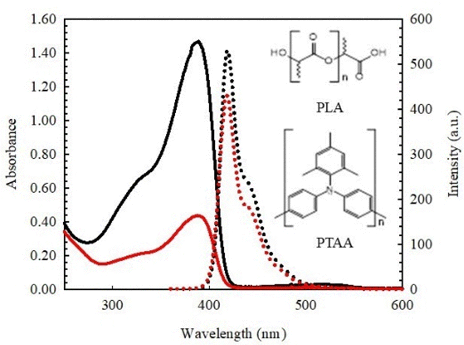 | ||
| Fig. 1 Absorption (solid lines – left scale) and emission (dotted lines – right scale) spectra of 2 wt%-PTAA (black) in CHCl3 and 5 wt%-PLA/PTAA (red) in CHCl3. Inset: Chemical structures of PLA and PTAA monomer basic unit. | ||
The UV/Vis spectra of 2 wt%-PTAA shows a high-intensity absorption band with a maximum at 388 nm attributed to π–π* transition of the conjugated molecular backbone.38,39 Furthermore, the emission spectrum of 2 wt%-PTAA solution in CHCl3 displayed a blue-green emission with a vibronic pattern exhibiting a maximum at 420 and 445 nm. The HOMO–LUMO energy gap, calculated from the crossing wavelength of the normalized absorption and emission spectra (409 nm) was found to be 3.03 eV, which is in excellent agreement with previous reports.40,41 Altogether, absorption and emission spectra of PLA/PTAA solutions measured in this study exhibit a remarkable consistency with those of PTAA in tetrahydrofuran (THF) and toluene.42,43 The similarity between the absorption and emission spectra of the 5 wt%-PLA/PTAA composite solution and those of pure PTAA, as shown in Fig. 1, confirms the uniformity of the composite and suggests the absence of any chemical reactions between PLA and PTAA. It is important to note that the color of the solutions remained unchanged for several days after being stored in a sealed vial under dark conditions, indicating good chemical stability.
SEM images of PLA/PTAA nanofibers at different concentrations prepared by Method 1, described in the experimental section, are presented in Fig. 2. These results suggest that for low PLA concentrations (<10 wt%) the solutions have small extensional viscosity44 and electrospinning failed to produce fibers. In such cases, during the electrospinning process, the solution is dispensed from the syringe in quirts behaving more as an electro-spraying technique. The polymer chains cannot stay intertwined while airborne as the solvent evaporates, and hence no fibers can form. It is observed in Fig. 2(a)–(h) is a spraying effect covering the cathode with randomly shaped polymer particles, since the polymer concentration is too low.
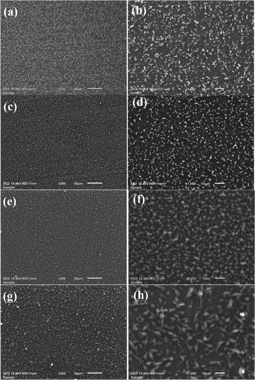 | ||
| Fig. 2 SEM images of electrospun fibers using solutions prepared by Method 1 of 1 wt%-PLA/PTAA – (a) low magnification (b) high magnification; 3 wt%-PLA/PTAA – (c) low magnification (d) high magnification; 5 wt%-PLA/PTAA – (e) low magnification (f) high magnification; 7 wt%-PLA/PTAA – (g) low magnification (h) high magnification. These fibers were prepared from the composite solutions before solvent evaporation. The white scale bar in (a), (c), (e), and (g) is 50 μm, and the white scale bar in (b), (d), (f) and (h) is 10 μm. | ||
The scant appearance of short-length fibers can be seen in Fig. 2(h) for the 7 wt%-PLA/PTAA sample. For reliable device fabrication, it is essential that the fibers are well-formed and electrically conducting, therefore, this approach of fiber fabrication needs to be modified.
It is known that to produce fibers via electrospinning, the solution to be electro-spun must have a large charge density and low surface tension.45 To fabricate long, well-formed, and bead-less PLA fibers at low concentrations, one needs to increase the viscosity and charge density of the solutions without polymer precipitation. Surprisingly, a simple solvent evaporation process, Method 2 described in the experimental section, just before electrospinning results in fiber formation. Images of PLA/PTAA fibers formed from electrospinning using Method 2 are shown in Fig. 3(a)–(h). Fig. 3(a) shows that a 1 wt% PLA/PTAA solution fails to produce fibers. At 3 wt%, Fig. 3(d) shows the formation of PLA/PTAA fibers, albeit there are many beads. PTAA assists in fiber formation and reducing the beading effect, as seen for the 5 and 7 wt% samples in Fig. 3(f) and (h). Image size analysis of the fibers results in diameters in the range 300–3000 nm. The modified process also renders the electro-spun fibers to be of high quality, especially for the 5 wt%-PLA/PTAA fibers as observed in Fig. 3(f). These fibers were long enough for device fabrication and could be electrically characterized. While a finite current was measured on the 5 wt%-PLA/PTAA fibers, no detectable current was observed for the fibers electro-spun from the 7 wt%-PLA/PTAA solution. These results are explained in terms of the higher PLA content, which prevented a continuous PTAA percolation path through the fibers. The absence of fibers in the electro-spun 1 wt% and 3 wt% solutions prevented us from doing fiber-based electrical characterization on these samples. Interestingly, the 5 wt%-PLA/PTAA solution produced more fibers than the 7 wt%-PLA/PTAA solution, as seen in Fig. 3(f) and (h).
 | ||
| Fig. 3 SEM images of electrospun fibers using solutions prepared by Method 2 of: 1 wt%-PLA/PTAA – (a) Low magnification (b) high magnification; 3 wt%-PLA/PTAA – (c) low magnification (d) high magnification; 5 wt%-PLA/PTAA – (e) low magnification (f) high magnification; 7 wt%-PLA/PTAA – (g) low magnification (h) high magnification. These fibers were prepared from the composite solutions after solvent evaporation. The white scale bar in (a), (c), (e) and (g) is 50 μm, and the white scale bar in (b), (d), (f) and (h) is 10 μm. | ||
Quantitative PTAA analysis by fluorescence
To better understand the effect of PLA/PTAA concentration on fiber formation, we determined the PTAA content in the solutions prepared for electrospinning just after solvent evaporation using the modified process, and after fiber formation. This is relevant because we propose an alternate sample preparation method for producing better homogeneity in fibers. PTAA has a strong fluorescence intensity resulting in an excellent probe that provides a sensitive method to determine its concentration. First, a calibration curve was obtained from stock solutions of PTAA in CHCl3. Fig. 4(a) shows the emission spectrum at different PTAA concentrations in the 0.0–6.0 × 10⁻⁴ mg mL−1 range.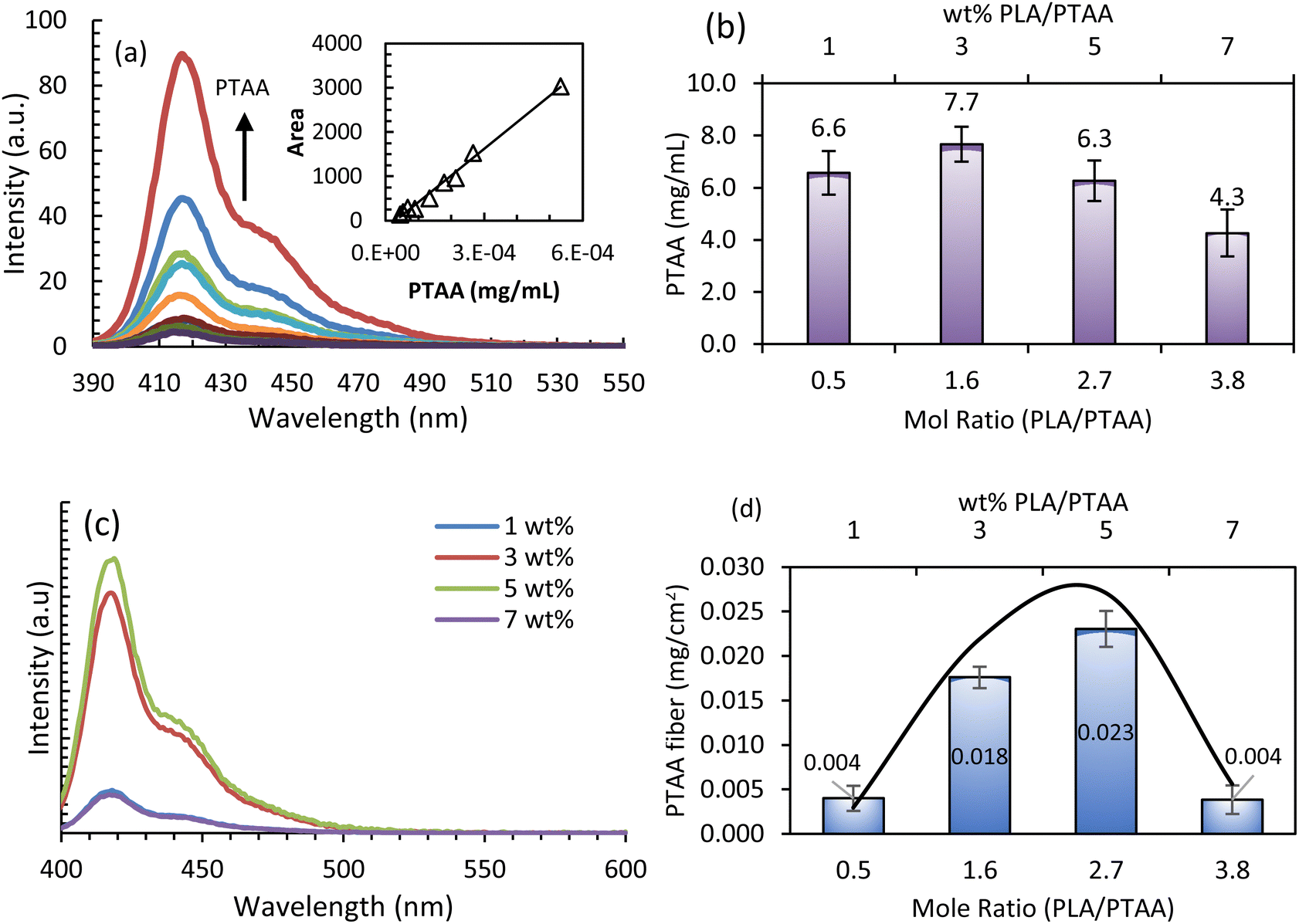 | ||
| Fig. 4 (a) Emission spectra of PTAA in CHCl3 at different concentrations from 0 to 6.0 × 10⁻⁴ mg mL−1 as indicated by the arrow; Inset: Calibration curve representing the area under emission curve vs. PTAA concentration (mg mL−1). The solid line represents the linear regression; (b) quantitative analysis of PTAA in the composite PLA/PTAA solution just after evaporation and before electrospinning; (c) emission spectra of PTAA present in composite nanofibers captured on the (∼ 2 × 2 cm2) aluminum foil and dissolved in CHCl3; (d) PTAA content in ∼2 × 2 cm2 nanofiber mat at each PLA/PTAA composite solution studied in this work, i.e., 1, 3, 5, and 7 wt%. Solid line represents a Gaussian function Y = (0.026 ± 0.002)exp[(−1/2) × (X-2.32 ± 0.07)2/(0.82 ± 0.09)2]. | ||
It can be observed from Fig. 4(a) that the shape of the emission spectra does not change with concentration. This suggests that PTAA does not aggregate or form excited state complexes under the experimental conditions. In addition, the intensity increases proportional to concentration. Thus, quantitative work can be performed using the PTAA emission spectra. Indeed, a linear relationship between emission area (A) and PTAA concentration was obtained as: A = mC + b with R2 = 0.9954, where m = (6.0 ± 0.2) × 106λ*(mg mL−1)−1, b = (−188 ± 50), C is the PTAA concentration in mg mL−1, and λ is the emission signal wavelength. To validate the calibration curve, a solution of 2.2 mg PTAA and 8.5 mg PLA in 0.637 mL CHCl3 was prepared and the PTAA content was determined using the calibration curve. The average relative determination error was 11% for 3 samples, as shown in Fig. S1 in the ESI.† Thus, the quantitative method to determine the PTAA concentration can be applied to the composite solutions and to the electrospun nanofibers after they are dissolved in CHCl3.
All the PLA/PTAA solutions prepared for electrospinning in this work have the same PTAA mass [0.11 g Part B (2 wt% PTAA/CHCl3) + 0.85 g Part A (X wt% PLA/CHCl3, where X is 1, 3, 5, or 7)] as mentioned earlier. After mixing Parts A and B and before solvent evaporation, the wt% of PLA are 0.9, 2.7, 4.4, and 6.2 for X = 1, 3, 5, and 7, respectively, and 0.23 wt% for PTAA. From these composite solutions, 0.50 g of solvent was evaporated before electrospinning to obtain high-quality fibers. After evaporation, the PLA wt% are 1.9, 5.7, 9.4, and 13.2, and 0.49 wt% of PTAA, for X = 1, 3, 5, and 7 respectively. The PTAA content in these solutions was determined experimentally by emission spectroscopy using the validated calibration curve. Fig. 4(b) shows that the PTAA content in the solutions remains constant within experimental error for 1, 3, and 5 wt%-PLA/PTAA solutions after solvent evaporation. A lower PTAA content is observed for the 7 wt%-PLA/PTAA but still close to the experimental error. After electrospinning, areas of ∼2 × 2 cm2 having maximum coverage of the PTAA/PLA film or PTAA/PLA nanofiber mat on the Al foil were cut from the 1, 3, 5, and 7 wt%-PLA/PTAA samples and dissolved in 2.00 mL CHCl3. The PTAA emission spectra for each X wt%-PLA/PTAA precursor solution, as obtained above, are shown in Fig. 4(c). It is observed that the shape of the PTAA emission spectrum remains like pure PTAA, meaning that it was not chemically modified. Fig. 4(d) shows the PTAA mass per 2 × 2 cm2 area for different mole ratio of PLA/PTAA solutions. It is observed that the mass of PTAA/cm2 increases from 1 to 5 wt%-PLA/PTAA and then decreases at 7 wt%-PLA/PTAA. These results, together with Fig. 3 suggest that PTAA, while present in the polymer deposit on the Al foil, is not necessarily incorporated into the nanofiber because in Fig. 3(a) to (d) there is no fiber present for 1 and 3 wt%-PLA/PTAA. Moreover, at 5 and 7 wt%-PLA/PTAA, fiber formation is observed (Fig. 3(e) to (h)). A lower quantity of fibers with larger diameters was observed for 7 wt%-PLA/PTAA compared to 5 wt%-PLA/PTAA. Altogether, these results demonstrate that for fiber formation, a minimum of 5 wt%-PTA/PLAA in the precursor solution is required under the proposed method. The 5 wt% PLA/PTAA results in 9.4 wt% after solvent evaporation. This is lower than that reported to date for conducting PLA composite nanofibers. Interestingly, if we take into consideration the average molecular weight of PTAA and PLA and plot the concentration of PTAA in the fiber mat per 2 × 2 cm2 as a function of PLA/PTAA mole ratio, a maximum of fiber formation occurs at 2.3-mole ratio of PLA/PTAA using a Gaussian function, as shown in Fig. 4(d). These results suggest that PTAA should be surrounded by a minimum of two PLA polymer chains to produce bead-less nanofibers. Using less than 5 wt% PLA leads to inadequate fiber formation, in agreement with previous reports. This could be due to lower viscosity, charge density, surface tension, and the proper incorporation of the appropriate amount of PTAA within the PLA polymer chains. On the other hand, using more than 5% wt in PLA results in fiber formation but with different physical and electrical properties, such as larger diameters and lower conductance. At 5% wt PLA, the modified method produced conductive fibers with lower diameters. This can be explained in terms of the correct alignment of the PLA polymer chains surrounding PTAA chains, and, in addition, PTAA–PTAA intermolecular distances are suitable for charge transfer. At 7 wt%-PLA/PTAA, excessive PLA polymer chains fail to incorporate PTAA between PLA chains (inadequate PTAA percolation). The inadequate PTAA percolation can result in lower charge transfer processes, ultimately decreasing fiber formation efficiency. The resulting fibers have a larger diameter and reduced conduction, meaning the resulting fiber shows higher PLA fiber characteristics. It is appropriate to note that if PTAA mass per 2 × 2 cm2 is normalized to the initial PTAA content just after evaporation, a Gaussian function like Fig. 4(d) is also obtained, as seen in Fig. S2 in the ESI.†
Electrical measurements
The electrical conductance of the composite fibers was examined to use them in a practical device like a junction diode. We chose the 5 wt%-PLA/PTAA sample since the fibers were long and of excellent quality, as seen in Fig. 3(f). The fibers formed from the 7 wt%-PLA/PTAA solution were not conducting, perhaps due to excess PLA that hinders PTAA percolation through the bulk of the fiber. The electrical response of a resistor device made of 5 wt%-PLA/PTAA fibers placed on a pre-patterned Si/SiO2 substrate is shown in Fig. 5. The optical image of the resistor is shown in Fig. 5 (inset). It shows two fibers lying across four “in-line” closely spaced (4 μm) Au electrodes patterned on the SiO2 layer. The I–V curve is linear and symmetrical when measured between two consecutive Au electrodes. The linearity was retained when the external connections to the device were reversed, implying that the fibers make Ohmic contact with the Au electrodes. The charged, flexible, and dry fibers obtained from electrospinning stick to the substrate on contact and cannot be moved without causing them to break. We therefore assume negligible contact resistance. The device conductance was 1.4 × 10⁻¹⁰ S, which is reasonable due to the small fiber dimensions and possible defects along the fiber length. The finite conductance, however confirms that PLA and PTAA do not phase separate but are uniformly blended in the “bulk” of the nanofiber, where PLA provides the mechanical support while PTAA the conduction path. In addition, the Ohmic contacts made with Au electrodes are important when analyzing the diode electrical response shown in Fig. 7 as explained below.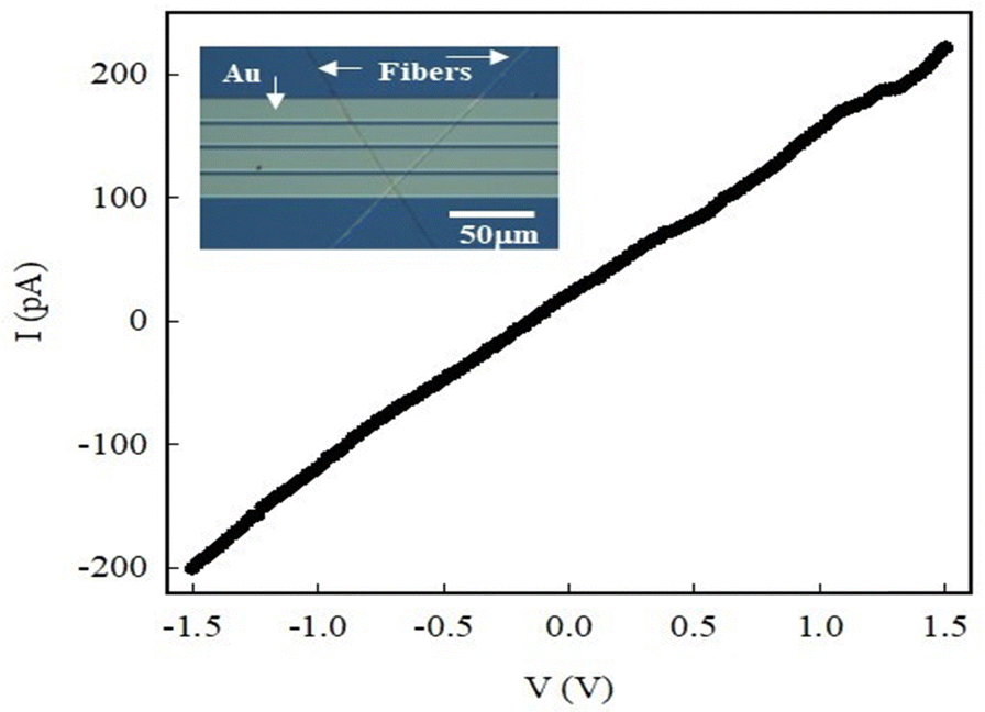 | ||
| Fig. 5 Current–voltage (I–V) plot of isolated 5 wt%-PLA/PTAA (modified process) nanofibers deposited on closely spaced gold contacts. Inset: Image of the fibers bridging four in-line Au electrodes. The contact resistance of the fibers with gold electrode is assumed negligible. | ||
The fabrication of a p–n junction diode is one of the many applications of these nanofibers. This device has two terminals and is fabricated using multiple fibers of 5 wt%-PLA/PTAA and a n-doped Si substrate. The device fabrication process begins with a pre-patterned n-Si/SiO2 (2000 Å oxide thickness) substrate that was cut through the Au electrodes as discussed elsewhere.46 Along the cleaved wafer edge lie many Au electrodes. The freshly cut substrate was fixed on the cathode (Al foil) to intercept the nanofibers emerging during the electrospinning process. It resulted in many nanofibers being deposited on the substrate surface, some of which crossed the wafer edge making permanent contact to the Au electrode at the edge and the n-doped Si along the cleaved surface. Fig. 6(a) shows a scanning electron microscope (SEM) image of the diode that was mounted at an angle with respect to the electron beam. Several continuous fibers can be seen bending over the wafer edge. A diagram of the diode and electrical contacts are shown in Fig. 6(b), and the p–n junction forms at the nanofibers/n-Si interface.46
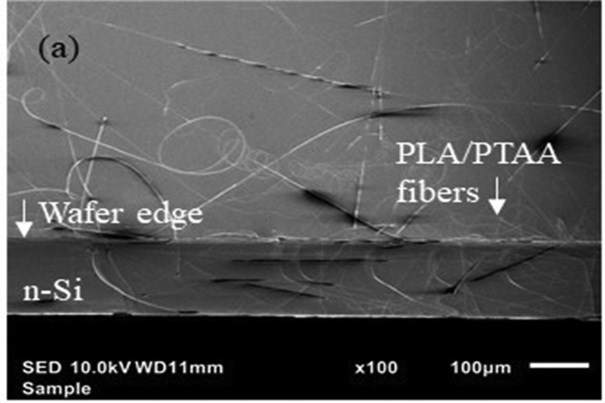 | ||
| Fig. 6 SEM image of the 5 wt%-PLA/PTAA nanofibers lying over the cleaved n-Si/SiO2 substrate. The substrate was mounted at an angle with respect to the electron beam to better view the cleaved surface. Some fibers are long enough that they cross over the wafer edge and physically make contact to the n-Si substrate. | ||
Fig. 7 presents the I–V plot at 295 K when the external power supply positive (+) terminal was connected to the Au electrode and the negative (−) terminal connected to n-Si. The fibers are known to make Ohmic contact with Au (Fig. 5); hence, the non-linear response seen in Fig. 7 (blue curve) arises from the p–n junction formed at the polymer nanofibers/n-Si substrate. This response is typical of a diode, where current flows in one direction and is blocked in the reverse. By interchanging the positive (+) and negative (−) terminals of the battery, the diode is turned on in the third quadrant of the I–V curve. This proves that the non-linear I–V behavior arises at the nanofiber/n-Si interface.
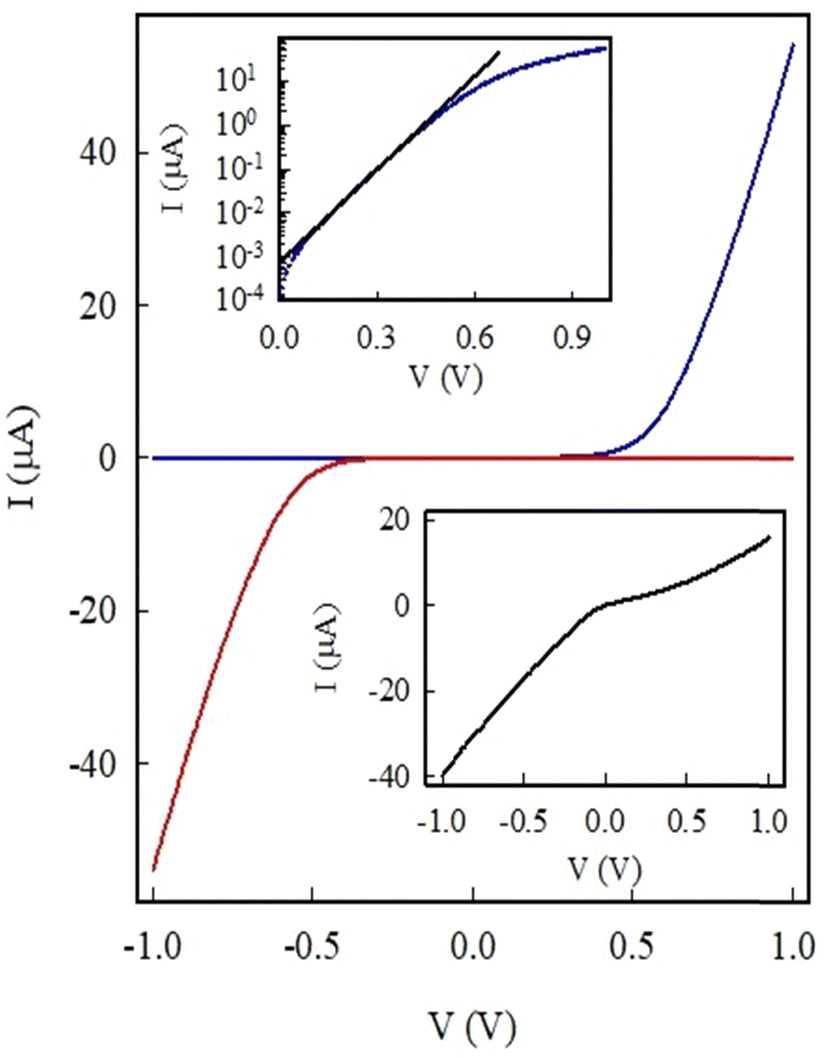 | ||
| Fig. 7 Diode I–V measurement. (Blue) I–V curve taken when the external battery positive terminal was connected to the Au electrode and the negative terminal connected to n-Si substrate. (Red) I–V curve taken when the external connections described above are reversed. Upper inset: Semi-logarithmic plot of I as a function of voltage (V > 0 – blue curve). Is the y-axis intercept of the straight-line fit. The slope of this line is used to calculate n. Lower inset: I–V curve of a similar diode using 5 wt%-PLA/PTAA nanofibers, but where the substrate was a pre-patterned p-Si/SiO2. | ||
When the 5 wt%-PLA/PTAA nanofibers were deposited on a p-Si/SiO2 substrates in a likewise fashion, and the device was electrically characterized, the I–V curve was relatively symmetric as expected, as seen in the band diagram (Fig. 8), once again confirming the presence of a p–n diode at the nanofibers/n-Si interface.
 | ||
| Fig. 8 Band diagram for the p–n junction diode under (a) equilibrium (b) forward bias and (c) reverse bias conditions. H and L represent the HOMO, LUMO levels in PTAA, while C and V represent the conduction band and valence band in n-Si. The Fermi energies in each material is represented by the dotted lines. | ||
The band gaps in PTAA and n-Si are known to be approximately 3.0 eV40,41 and 1.12 eV,46,47 respectively. The non-linear I–V curve observed in the plot can be attributed to the diffusion of electrons and polarons across the PLA/PTAA junction, leading to charge neutralization and the establishment of a charge-free region with a constant Fermi energy level due to band bending at the interface (Fig. 8(a)). The result is a potential barrier that inhibits further charge flow across the junction unless an external voltage is applied. Forward biasing the diode enables current flow, while reverse biasing inhibits it, as shown in the band diagrams of Fig. 8(b) and (c). When the external voltage (+) terminal is applied to the p-arm of the device, it is forward biased, and current can flow. When the voltage on the p-arm of the diode is (−) with respect to the n-arm, the diode is reverse-biased, and no current can flow. These changes are depicted in the band diagrams of Fig. 8(b) and (c). The current–voltage relationship for the forward biased-biased diode can be described by the equation I = Is[exp(eV/nkBT) − 1], where Is is the reverse bias saturation current, e is the electronic charge, and n is the ideality factor; kB and T represent the Boltzmann constant and temperature.47 The values of Is and n were determined to be 800 pA and 2.1, respectively, using a semi-log plot of I–V under forward bias (Fig. 7, upper inset). This diode on/off ratio at ±1 V was calculated to be ∼800, with limitations arising from the polymer resistance, bulk n-Si resistance, and finite contact resistance at the metal/fiber contact. The current when the diode is turned on is much higher than the current measured in the device shown in Fig. 5(inset). This is because of the extremely small (200 nm) length of the fiber arm of the diode compared to the length of 4 μm fiber length in the device measured in Fig. 5(inset). The diode turn-on occurred at 0.6 V making it suitable for handheld instruments and wearable electronics.
Diodes are electronic circuit components that are primarily used for signal rectification (AC to DC conversion). They play an important role in our everyday energy and communication technology such as power supplies, smartphones, and other hand-held electronic devices. The diode action on an AC signal was tested and the results are shown in Fig. 9.
 | ||
| Fig. 9 Diode used as a half-wave rectifier. A 5 V, 10 Hz input signal (i/p black curve) was applied to the diode and the output (o/p blue curve) measured across the load resistor. Inset: Schematic of the diode circuit used for rectification. | ||
The input was a full sine wave 10 Hz signal, while the output measured across the load resistor was clipped. Fig. 9 shows the oscilloscope traces of the input and output signals. The two signals are in phase; however, the negative cycle of the output signal is suppressed. The ratio of the output power to the input power was ∼15%. For comparison, 40% is the rectifier efficiency of a commercial diode used as a half-wave rectifier. Fig. 9 is therefore proof that the diode is a reliable half-wave rectifier and hence can be used as a building block in advanced electronics.
Conclusions
Electrically conducting PLA/PTAA composite nanofibers were successfully fabricated for the first time at PLA concentrations <10 wt% in CHCl3. UV-Vis and fluorescence spectroscopy confirm uniform incorporation of PTAA into the blend. Quantitative PTAA concentration as determined via emission spectra show that the highest PTAA content in the fibers was at 5 wt%-PLA/PTAA. The 5 wt%-PLA/PTAA solution also produced an abundance of long and uniform composite nanofibers compared to other concentrations. By using our modified technique of monitored solution evaporation, the fibers made from 5 wt%-PLA/PTAA were electrically conducting. These fibers were then used to fabricate a diode utilizing an n-doped silicon substrate. This diode had a turn-on voltage of 0.6 V, a rectification ratio of 800 and an ideality parameter of 2.1. In addition, the diode was employed as a half-wave rectifier and operated at 15% rectification efficiency. Making PLA electroactive with PTAA potentially expands the use of this biocompatible and biodegradable polymer. Some applications of these nanofibers include diodes, transistors, sensors, medical implants, and healthcare devices.Data availability
The authors state that all the data presented in this manuscript will be made available upon request.Author contributions:
Conceptualization and methodology, W. S-G, N. J. P., and R. O.; experimental procedures, A. J. C., N. V. F-C., and R. O.; writing and editing, W. S-G., N. J. P., and R. O. All authors have read and agreed to the published version of the manuscript.Conflicts of interest
The authors declare no competing financial interest.Acknowledgements
This work was supported by NSF-DMR under grant DMR-2122102.References
- R. Ghosh, K. Y. Pin, V. S. Reddy, W. A. D. M. Jayathilaka, D. Ji, W. Serrano-García, S. K. Bhargava, S. Ramakrishna and A. Chinnappan, Appl. Phys. Rev., 2020, 7, 041309 CAS.
- B. Guo, L. Glavas and A.-C. Albertsson, Prog. Polym. Sci., 2013, 38, 1263–1286 CrossRef CAS.
- W. A. D. M. Jayathilaka, K. Qi, Y. Qin, A. Chinnappan, W. Serrano-García, C. Baskar, H. Wang, J. He, S. Cui, S. W. Thomas and S. Ramakrishna, Adv. Mater., 2019, 31, 1805921 CrossRef PubMed.
- R. A. Giordano, B. M. Wu, S. W. Borland, L. G. Cima, E. M. Sachs and M. J. Cima, J. Biomater. Sci., Polym. Ed., 1997, 8, 63–75 CrossRef PubMed.
- S. A. Stewart, J. Domínguez-Robles, V. J. McIlorum, E. Mancuso, D. A. Lamprou, R. F. Donnelly and E. Larrañeta, Pharmaceutics, 2020, 12, 105 CrossRef CAS PubMed.
- H. Hou, Z. Jun, A. Reuning, A. Schaper, J. H. Wendorff and A. Greiner, Macromolecules, 2002, 35, 2429–2431 CrossRef CAS.
- K. Kim, M. Yu, X. Zong, J. Chiu, D. Fang, Y.-S. Seo, B. S. Hsiao, B. Chu and M. Hadjiargyrou, Biomaterials, 2003, 24, 4977–4985 CrossRef CAS PubMed.
- X. M. Mo, C. Y. Xu, M. Kotaki and S. Ramakrishna, Biomaterials, 2004, 25, 1883–1890 CrossRef CAS PubMed.
- W. Serrano, A. Meléndez, I. Ramos and N. J. Pinto, Polymer, 2014, 55, 5727–5733 CrossRef CAS.
- W. Serrano, A. Meléndez, I. Ramos and N. J. Pinto, 2014.
- W. Serrano, A. Meléndez, I. Ramos and N. J. Pinto, Polym. Int., 2016, 65, 503–507 CrossRef CAS.
- H. Tsuji, M. Nakano, M. Hashimoto, K. Takashima, S. Katsura and A. Mizuno, Biomacromolecules, 2006, 7, 3316–3320 CrossRef CAS PubMed.
- K. I. Kwon, S. Kidoaki and T. Matsuda, Biomaterials, 2005, 26, 3929–3939 CrossRef PubMed.
- Z. Gan, Y. Zhao, Y. Wu, W. Yang, Z. Zhao and L. Zhao, Acta Biomater., 2022, 147, 221–234 CrossRef CAS PubMed.
- S. D. McCullen, K. L. Stano, D. R. Stevens, W. A. Roberts, N. A. Monteiro-Riviere, L. I. Clarke and R. E. Gorga, J. Appl. Polym. Sci., 2007, 105, 1668–1678 CrossRef CAS.
- R. A. Qazi, M. S. Khan, L. A. Shah, R. Ullah, A. Kausar and R. Khattak, Polym.-Plast. Technol. Mater., 2020, 59, 928–951 CAS.
- R. Scaffaro, L. Settanni and E. F. Gulino, Molecules, 2023, 28(4), 1967 CrossRef CAS PubMed.
- J.-h Wu, T.-g Hu, H. Wang, M.-h Zong, H. Wu and P. Wen, J. Agric. Food Chem., 2022, 70, 8207–8221 CrossRef CAS PubMed.
- T. Yang, D. Wu, L. Lu, W. Zhou and M. Zhang, Polym. Compos., 2011, 32, 1280–1288 CrossRef CAS.
- H. Y. Chi, V. Chan, C. Li, J. H. Hsieh, P. H. Lin, Y.-H. Tsai and Y. Chen, BMC Chem., 2020, 14, 63 CrossRef CAS PubMed.
- F. Imani, R. Karimi-Soflou, I. Shabani and A. Karkhaneh, Polymer, 2021, 218, 123487 CrossRef CAS.
- W. Serrano-Garcia, W. A. D. M. Jayathilaka, A. Chinnappan, T. Q. Tran, C. Baskar, S. W. Thomas and S. Ramakrishna, Sci. China: Technol. Sci., 2019, 62, 895–902 CrossRef.
- J. Smith, W. Zhang, R. Sougrat, K. Zhao, R. Li, D. Cha, A. Amassian, M. Heeney, I. McCulloch and T. D. Anthopoulos, Adv. Mater., 2012, 24, 2441–2446 CrossRef CAS PubMed.
- S. Heun and P. M. Borsenberger, Phys. B, 1995, 216, 43–52 CrossRef CAS.
- H. J. Ha, M. G. Kim, J. H. Ma, J. H. Jeong, M. H. Park, S. J. Kang, W. Kim, S. Park and S. J. Kang, Sci. Rep., 2023, 13, 3780 CrossRef CAS PubMed.
- H.-H. Cho, L. Yao, J.-H. Yum, Y. Liu, F. Boudoire, R. A. Wells, N. Guijarro, A. Sekar and K. Sivula, Nat. Catal., 2021, 4, 431–438 CrossRef CAS.
- A. Das, R. Dost, T. Richardson, M. Grell, J. J. Morrison and M. L. Turner, Adv. Mater., 2007, 19, 4018–4023 CrossRef CAS.
- J. H. Heo, S. H. Im, J. H. Noh, T. N. Mandal, C.-S. Lim, J. A. Chang, Y. H. Lee, H.-J. Kim, A. Sarkar, M. K. Nazeeruddin, M. Grätzel and S. I. Seok, Nat. Photonics, 2013, 7, 486–491 CrossRef CAS.
- Y. Ko, Y. Kim, C. Lee, Y. Kim and Y. Jun, ACS Appl. Mater. Interfaces, 2018, 10, 11633–11641 CrossRef CAS PubMed.
- M.-B. Madec, J. J. Morrison, V. Sanchez-Romaguera, M. L. Turner and S. G. Yeates, J. Mater. Chem., 2009, 19, 6750–6755 RSC.
- K. Masumura, I. Nakanishi, K. Van Thi Khuat, K. Kinashi, W. Sakai and N. Tsutsumi, Sci. Rep., 2019, 9, 739 CrossRef PubMed.
- F. M. Rombach, S. A. Haque and T. J. Macdonald, Energy Environ. Sci., 2021, 14, 5161–5190 RSC.
- J. Smith, R. Hamilton, I. McCulloch, M. Heeney, J. E. Anthony, D. D. C. Bradley and T. D. Anthopoulos, Synth. Met., 2009, 159, 2365–2367 CrossRef CAS.
- J. Veres, S. D. Ogier, S. W. Leeming, D. C. Cupertino and S. Mohialdin Khaffaf, Adv. Funct. Mater., 2003, 13, 199–204 CrossRef CAS.
- W. Zhang, J. Smith, R. Hamilton, M. Heeney, J. Kirkpatrick, K. Song, S. E. Watkins, T. Anthopoulos and I. McCulloch, J. Am. Chem. Soc., 2009, 131, 10814–10815 CrossRef CAS PubMed.
- R. Cai and A. M. Jonas, Sci. Rep., 2016, 6, 22116 CrossRef CAS PubMed.
- O. Martínez, A. G. Bravo and N. J. Pinto, Macromolecules, 2009, 42, 7924–7929 CrossRef.
- T. Kurata, K. Koshika, F. Kato, J. Kido and H. Nishide, Polyhedron, 2007, 26, 1776–1780 CrossRef CAS.
- H.-Y. Wang, G. Chen, X.-P. Xu, H. Chen and S.-J. Ji, Dyes Pigm., 2011, 88, 358–365 CrossRef CAS.
- A. Intaniwet, C. A. Mills, M. Shkunov, H. Thiem, J. L. Keddie and P. J. Sellin, J. Appl. Phys., 2009, 106, 064513 CrossRef.
- B. R. Saunders and M. L. Turner, Adv. Colloid Interface Sci., 2008, 138, 1–23 CrossRef CAS PubMed.
- J. R. Klein, M. Scholz, K. Oum and T. Lenzer, Photochem. Photobiol. Sci., 2018, 17, 722–733 CrossRef CAS PubMed.
- J. H. Yu, S. V. Fridrikh and G. C. Rutledge, Polymer, 2006, 47, 4789–4797 CrossRef CAS.
- D. H. Reneker and A. L. Yarin, Polymer, 2008, 49, 2387–2425 CrossRef CAS.
- N. J. Pinto, R. González, A. T. Johnson and A. G. MacDiarmid, Appl. Phys. Lett., 2006, 89, 033505 CrossRef.
- A. J. Cruz-Arzon, K. S. Figueroa, N. J. Pinto, Z. Qicheng, C. Kehayias, S. Yeonjoon and A. T. C. Johnson, Synth. Met., 2022, 283, 116967 CrossRef CAS.
- S. M. Sze and K. N. Kwok, Physics of Semiconductor Devices, John Wiley & Sons, Inc., 3rd edn, 2006, ch. 3, pp. 77–133 DOI:10.1002/9780470068328.ch2.
Footnote |
| † Electronic supplementary information (ESI) available. See DOI: https://doi.org/10.1039/d3ma00230f |
| This journal is © The Royal Society of Chemistry 2023 |