
 Open Access Article
 This Open Access Article is licensed under a Creative Commons Attribution-Non Commercial 3.0 Unported Licence
Broadband photoresponse in plasmon-enhanced Ga-doped ZnO†
Manli
Yang‡
,
Xiaoliang
Weng‡
 ,
Muhammad Ahsan
Iqbal
,
Chenxu
Kang
,
Su-Yun
Zhang
and
Yu-Jia
Zeng
*
,
Muhammad Ahsan
Iqbal
,
Chenxu
Kang
,
Su-Yun
Zhang
and
Yu-Jia
Zeng
*
Key Laboratory of Optoelectronic Devices and Systems of Ministry of Education and Guangdong Province, College of Physics and Optoelectronic Engineering, Shenzhen University, Shenzhen 518060, Guangdong, China. E-mail: yjzeng@szu.edu.cn
First published on 5th April 2023
Abstract
In recent decades, zinc oxide (ZnO) has received considerable attention as a wide direct bandgap semiconductor for high-performance ultraviolet optoelectronic devices. However, ZnO-based photodetectors suffer from intrinsic challenges that limit their performance in fast-response and broadband photodetection. Herein, we develop Ga-doped ZnO (GZO) photodetectors with localized surface plasmon resonance (LSPR) properties. Ga doping extends the optical response range of ZnO devices to the near-infrared region (1064 nm). Furthermore, the photothermoelectric (PTE) effect results in an intriguing current polarity reversal phenomenon. Finally, the coupling of black phosphorus nanocrystals further improves the performance of the photodetector. This study provides a promising noble-metal free plasmon-enhanced photodetector, which has great potential for use in broadband photodetection and bipolar signal communication.
Introduction
Photodetectors are devices that convert optical signals into electrical signals, and have a wide range of applications from everyday life to the military field.1–7 Zinc oxide (ZnO) is an n-type wide direct bandgap (3.37 eV) semiconductor that is useful in ultraviolet (UV) optoelectronics. In comparison to other competing materials, such as GaN, ZnO has a higher exciton binding energy (ZnO: 60 meV and GaN: 26 meV) and a higher visible band transparency (>80%).8–11 It is difficult to produce high-quality p-type ZnO because of its native defects, such as oxygen vacancies and zinc interstitials, which is still a drawback in optoelectronic applications based on ZnO p–n heterojunctions.12–14 Moreover, ZnO exhibits a limited spectral response only in the UV range. As a result, an effective mechanism to extend the optical response range of ZnO devices is of great interest.Doping is a frequently employed technique for changing the characteristics of semiconductor materials, including carrier concentration, localized surface plasmon resonance (LSPR), electrochemical potential, and so on.15–18 Prior studies to increase ZnO conductivity include substituting B,19 Al,20 Ga,21 and In22 for Zn and substituting F for O. Ga appears to be one of the best options when taking into account the stability, simplicity and cost.23–25 n-Type doping may result in an LSPR effect, which could greatly enhance the photoelectric properties of semiconductor materials.26–28 It has also been reported that Ga doping may induce infrared emission from ZnO.29,30 Doped plasmonic semiconductors have lower prices and tunable photoelectric properties when compared to noble metal materials, such as Au and Ag, and are expected to become effective substitutes for noble metals.31,32
Many mainstream technologies can be applied to the preparation of doped ZnO thin films. In this study, controllable magnetron sputtering technology is used to obtain uniform, dense, and stable high-quality Ga-doped ZnO (GZO) films. GZO films have strong absorption in both ultraviolet and near-infrared bands, while the optical response range of a self-powered photodetector based on the GZO film covers the UV-Vis-NIR band (365–1064 nm) owing to the LSPR effect resulting from Ga doping. The prepared doped ZnO based device shows an interesting current polarity reversal phenomenon in a wide band due to the photothermoelectric effect (PTE). Furthermore, the heterojunction is built by combining GZO and black phosphorus (BP) nanocrystals (NCs) that have been prepared in a liquid phase. BP is an emerging 2D material with diverse applications, and can be combined with various semiconductors for heterojunctions.33,34 The heterojunction significantly boosts the device's responsivity and response speed over a broad spectral range. In conclusion, the simultaneous application of doping and heterojunctions enhances the optical response performance of ZnO-based devices and offers a new approach for the future development of broadband photodetectors.
Experimental
Growth of GZO thin films and device fabrication
Ga-doped ZnO thin films were obtained by RF magnetron sputtering using Ga-doped ZnO targets with atomic ratios of 0%, 2%, and 5%. Si, Si/SiO2 and quartz substrates were cleaned with acetone, alcohol and ultra-pure water. A power source of 100 W was used during deposition, and the growth temperature was maintained at 400 °C for 60 min. Ti/Au (I-shaped with a 50 nm thickness) was deposited as the electrode.Preparation of BP NCs
Ultrasonic-assisted exfoliation was used to prepare BP NCs. BP powder was placed in a nitrogen glove box and weighed using a brown glass bottle to prevent it from being oxidized. The glass was then sealed after being filled with NMP solvents. The mixture was subjected to ten 30 min ultrasonic cycles. A black dispersion with BP nanocrystals and nanosheets was obtained. The resultant was then transferred to a centrifuge tube for gradient centrifugation purification to separate BP NCs. Finally, BP NC precipitates were mixed with a fresh NMP solution and stored to produce a bright yellow nanocrystalline dispersion. 0%, 2%, and 5% Ga-doped GZO thin film photodetector devices were coated with the BP NC solution, and the devices were then dried for 6 h in a vacuum drying oven. After the NMP solution was completely evaporated, the BP-enhanced photodetector was obtained.Characterization
The surface morphology information was obtained using a field emission scanning electron microscope (SEM, ZEISS, Sigma 300). X-ray diffraction (XRD) spectra were obtained using an X-ray powder diffractometer (Rigaku, ULTIMA IV). X-ray photoelectron spectroscopy (XPS, Thermo Fisher, Thermo Nicolet iS5) was used for energy spectrum analysis. The transmission spectra were obtained using a Fourier transform infrared spectrometer (FTIR, Bruker, VERTEX 80/80v). The ultraviolet/visible/near-infrared (UV-Vis-NIR) optical absorption spectra of the films were obtained in the range of 300–2500 nm using a Lambda 950 spectrophotometer. The high-resolution images of nanocrystals were obtained by high-resolution transmission microscopy (JEOL, JEM-F200). Raman scattering spectra were collected using a Raman spectrometer (Horiba, LabRAMHR Evolution) with an excitation wavelength of 514 nm. Hall effect measurements were carried out in the van der Pauw configuration. The photoelectric test of the device was carried out in a double probe mode using a Keysight B2902A digital electricity meter.Results and discussion
GZO thin films are prepared by magnetron sputtering on various substrates, including Si, Si/SiO2, and quartz substrates. The SEM surface morphology and cross-section images of ZnO and GZO thin films are shown in Fig. 1a–d. The surface morphology of the thin films demonstrates their firmness, good adhesion, and uniformity. The SEM surface morphology shows that the doping concentration of Ga atoms has an impact on the surface morphology of the films, which reduces the grain size of the film. However, GZO films still show a smooth surface. A cross-sectional image of the 2% GZO film is shown in Fig. 1d, which shows a uniform thickness of approximately 300 nm.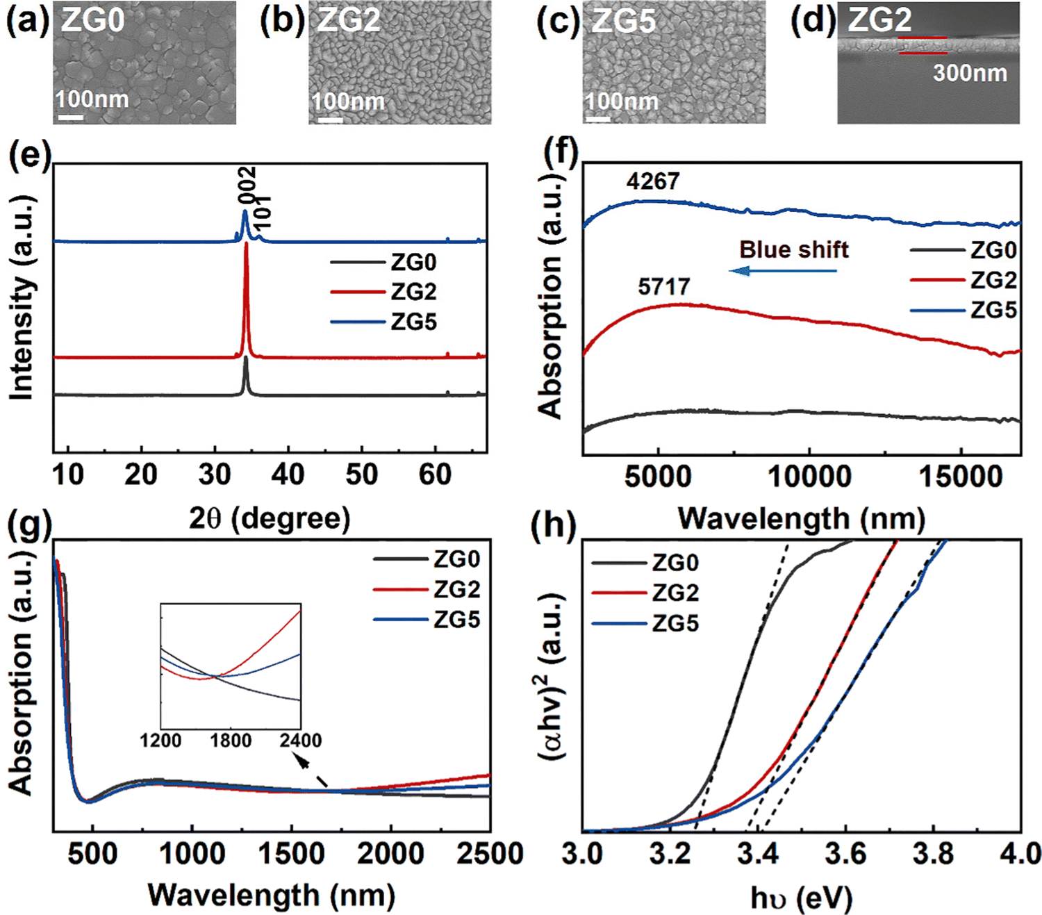 | ||
| Fig. 1 (a)–(c) SEM images of ZG0, ZG2 and ZG5 thin films. (d) Cross-section image of the ZG2 thin film. (e) XRD patterns of ZG0, ZG2 and ZG5 thin films. (f) FTIR absorption spectra of ZG0, ZG2 and ZG5 thin films. (g) UV-Vis-NIR absorption spectra of ZG0, ZG2 and ZG5 thin films. (h) Relationship between (αhv)2 and photon energies of ZG0, ZG2 and ZG5 thin films. | ||
To study the effect of Ga doping concentration on the optoelectronic properties, ZnO and GZO thin film devices with different doping concentrations (Ga = 2 at% and 5 at%) are used and are named ZG0, ZG2 and ZG5, respectively. Fig. 1e shows the XRD patterns of GZO films of different doping concentrations (Ga = 0 at%, 2 at%, and 5 at%). A clear (002) peak and a less obvious (101) peak can be seen, which are consistent with the typical diffraction peaks of ZnO, and other peaks are the signals of the Si substrate. With the increase in the Ga doping concentration, the (002) peak first increases and then decreases. The undoped ZnO film does not show the (101) peak,35 which is owing to the better crystal quality as compared to the Ga-doped samples. Fig. 1f shows the infrared absorption spectra of GZO thin films deposited on the Si substrate. The undoped ZnO film has no absorption peak, while ZG2 and ZG5 thin films show clear broad LSPR peaks at 5716 nm and 4267 nm, respectively. With the increase of the doping concentration, an obvious blue shift of the peak is observed, and the peak intensity of the ZG2 film is significantly stronger than that of the ZG5 film. Fig. 1g shows the UV-Vis-NIR absorption spectrum of the GZO film on the quartz substrate.36–38 GZO films with different doping concentrations have good transmittance in the visible light range. The optical band gap values of ZG0, ZG2 and ZG5 films are 3.25, 3.37, and 3.41 eV, respectively, as shown in Fig. 1h. The doping of Ga causes an increase in carrier concentration. As a result, the Fermi level shifts to the conduction band, causing the Burstein-Moss effect, which widens the optical band gap. In addition, Hall effect measurements were performed to obtain the carrier concentrations of ZG2 and ZG5 films, which give the electron carrier concentrations in the range of 1–2 × 1021 cm−3. This high concentration in the semiconductor is believed to result in the LSPR band in the near infrared region,39 which is consistent with increased absorption in the near infrared region as shown in the inset of Fig. 1g.
The chemical composition and the valence state of the film were studied by XPS measurements. XPS spectra are shown in Fig. 2 after calibration by a C1s binding energy of 284.8 eV. Fig. 2a shows that the ZnO film contains Zn and O elements. Fig. 2b shows Ga 2p spectra in ZG0, ZG2 and ZG5 films. The obvious Ga element peak is observed from 1117 to 1145 eV, which increases with the Ga concentration. Fig. 2c shows Zn 2p spectra in ZnO and GZO films. The Zn 2p3/2 and Zn 2p1/2 spectra observed at 1020 to 1045 eV are determined by the binding energy of Zn–O. The bimodal spacings are 23.1 and 23.2 eV, indicating that the Zn element in the film exists only in the form of a +2 valence oxidation state, that is, the Zn–O bond in the ZnO lattice.28,40 In addition, no other elements are observed, reflecting the high purity of the prepared samples.
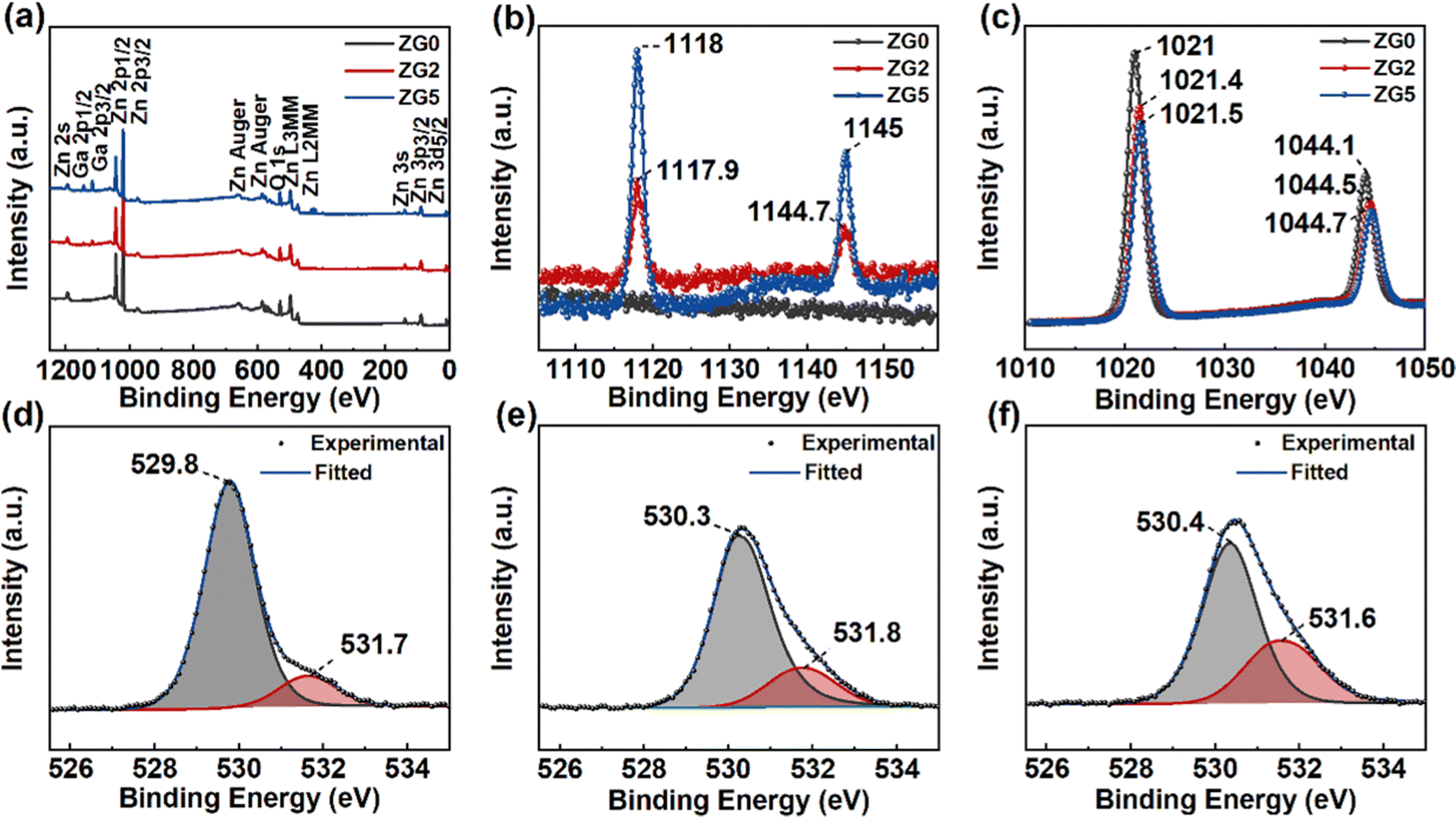 | ||
| Fig. 2 (a) XPS wide scan spectra of ZG0, ZG2 and ZG5 thin films. (b) XPS spectra of the Ga 2p of ZG0, ZG2 and ZG5 thin films. (c) XPS spectra of the Zn2p of ZG0, ZG2 and ZG5 thin films. XPS spectra of the O1s of GZ0 (d), GZ2 (e), and GZ5 (f) thin films. | ||
Fig. 2d–f shows the narrow scanning XPS spectra of O1s peaks of ZnO and GZO thin films. After Gaussian fitting, two types of O-levels are observed on the asymmetric peaks. The lower binding energy (O I) peak comes from the bonding between O2+ and metal ions in the hexagonal wurtzite lattice (Zn–O or Ga3+ Ga–O bond), while the higher binding energy (O II) peak corresponds to the O vacancy or surface adsorption of C–O bonds due to the exposure to the surrounding environment, which increases with the Ga concentration. Assuming the surface adsorption is the same, these results indicate that the concentration of O vacancies increases with Ga doping, which could contribute to the n-type conduction.41
BP NCs were prepared using a simple liquid phase preparation technique to improve the optical response performance of doped ZnO devices.42,43Fig. 3a shows the absorption spectrum of BP NCs. The image of the dispersion is shown inset. BP NCs are dissolved in the NMP solution and are transparent yellow. When irradiated using a laser pen, an obvious Tyndall phenomenon indicates the good dispersion. The absorption curve shows that BP NCs can absorb light in the wavelength range of 350–900 nm. The whole curve is relatively flat, and there is an obvious absorption peak at approximately 385 nm. Also, the absorption spectrum of the ZnO/BP heterojunction is shown in Fig. S1 (ESI†), suggesting both absorptions of ZnO and BP. Fig. 3b shows the Raman spectra of BP NCs and bulk BP. The Raman peaks of BP nanocrystals are located at 361.81 cm−1, 439.20 cm−1, and 467.33 cm−1, which correspond to the three atomic vibration modes of A1g, B2g, and B2g, respectively.40,41Fig. 3c and d show the HRTEM images of the synthesized BP nanoparticles with a relatively uniform morphology. The size of the nanoparticles is approximately 5–20 nm. The illustration in Fig. 3d shows that the lattice spacing of BP nanoparticles is 0.252 nm. The results show that BP nanocrystals with good quality have been successfully prepared.
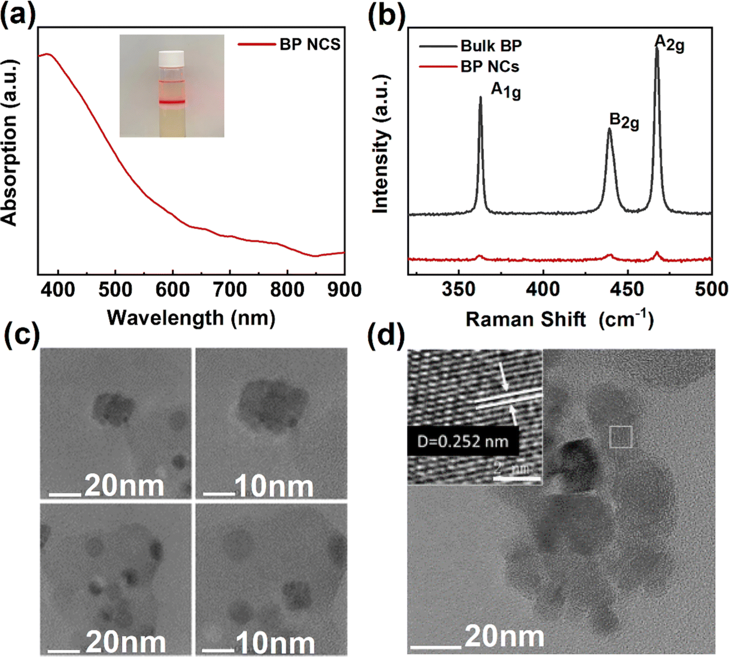 | ||
| Fig. 3 Characterization of BP NCs prepared in a liquid phase. (a) BP NCs absorption spectrum. (b) Raman spectra of BP NCs and bulk BP. (c) and (d) HRTEM images of BP NCs. | ||
A schematic diagram of the photodetector device is shown in Fig. 4a. Fig. 4b shows the I–V curve of thin film devices in the dark. Upon illumination, as shown in Fig. 4c, the current of each device increases significantly. At 0 V, the photocurrents of ZG0, ZG2, and ZG5 are 0.002 μA, 0.805 μA, and 0.268 μA, respectively. As shown in the embedded diagram in Fig. 4c, ZG0 also has an obvious I–V response curve. There is an obvious photovoltaic effect without any applied voltage, and the introduction of the Ga atom is conducive for improving the optical response performance of the device. Fig. 4d shows the light response behavior of the device under periodic UV irradiation. With the switching of the light source, the current increases and decreases rapidly, and the device has good periodicity and sensitivity.
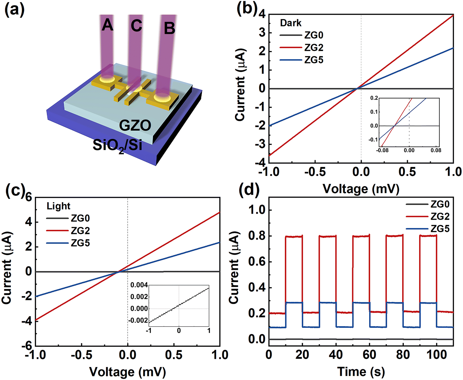 | ||
| Fig. 4 (a) Schematic diagram of the thin film photodetector device illuminated at different positions (electrode A, electrode B, and C: channel). (b) Dark currents of ZG0, ZG2, and ZG5 devices (inset is the enlarged view near zero voltage). (c) Photocurrents of ZG0, ZG2, and ZG5 devices at 365 nm (inset is the I–V curve of ZG0). (d) I–t curves of ZG0, ZG2, and ZG5 devices at 365 nm. | ||
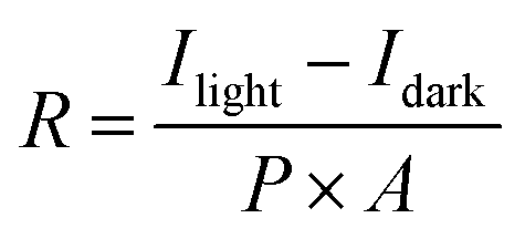
To further quantitatively analyze the photoresponse performance of the device after Ga doping, the parameters such as responsivity (R) and detectivity (D*) are calculated. The responsivity represents the device's response efficiency to incident light and is calculated using the following formula:42
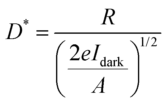
where Δf is the electronic bandwidth, and in is the noise current. There are three kinds of noise limiting D*: shot noise from the dark current, Johnson noise, and “chattering” noise generated by thermal disturbance. Generally, the dark current is mainly controlled by shot noise. At the same time, the current cross-sectional area can be approximately replaced by the optical area, so the expression of D* becomes:45
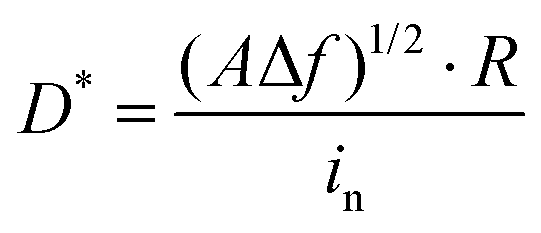
where e is the absolute value of electron charge. The detectivities of ZG0, ZG2, and ZG5 are shown in Table 1. Again, ZG2 has the highest detection. We further calculate the response time of the devices. The ZG2 device has a fast response, and the τrise and τdecay values are 15.3 ms and 18 ms, respectively.
| R (mA W−1) | D* (Jones) | τ rise (ms) | τ decay (ms) | |
|---|---|---|---|---|
| ZG0 | 3.523 × 10⁻² | 2.328 × 10¹⁰ | 81.3 | 32.8 |
| ZG2 | 9.993 | 1.773 × 10¹¹ | 15.3 | 18 |
| ZG5 | 3.253 | 8.49 × 10¹⁰ | 31.5 | 31.5 |
| BZG0 | 9.447 × 10⁻² | 6.308 × 10¹⁰ | 135.4 | 21.5 |
| BZG2 | 12.86 | 2.295 × 10¹¹ | 1 | 6.7 |
| BZG5 | 4.631 | 1.278 × 10¹⁰ | 2.4 | 7.6 |
Next, the broadband optical response characteristics of ZnO and GZO thin film devices in the UV-Vis-NIR (365–1064 nm) range are studied. The power density is unified at 5 mW cm−2. The results show that ZG0 exhibits self-powered properties only at 365 nm, while ZG2 and ZG5 exhibit good broadband optical response performance from 365 to 1064 nm, which is beyond the band gap of ZnO and is believed to result from the LSPR effect. The wavelength-dependent responsivities of the ZG2 device can be seen in Fig. S2 (ESI†). As shown in Fig. 5a, the self-powered performance of ZG2 is better than that of ZG5 in each wavelength. In addition, an interesting polarity switching phenomenon is observed. When the light source is illuminated at different electrodes, the direction of the photocurrent flips. Fig. 5b shows the test results at 365 nm with a power intensity of 30 mW cm−2. It shows that ZG0, ZG2, and ZG5 all have polarity switching behavior, and ZG2 has the best photoresponse performance. The photocurrent is positive when the light source is at one end of the electrode. The photocurrent decreases as light gathers in the channel. The photocurrent reverses when the light source is close to the other end electrode. The curve in the figure represents the current value measured when the temperature asymmetry caused by laser radiation local heating is greatest, which is a typical PTE. Through the temperature gradient on the two electrodes, it generates potential in light radiation. The hot end carriers migrate to the cold end as a result of this field, determining the direction of the current. Our results are consistent with previous reports on the PTE phenomenon,12,46–48 which confirms that the PTE effect plays a role in the observed photoresponse.
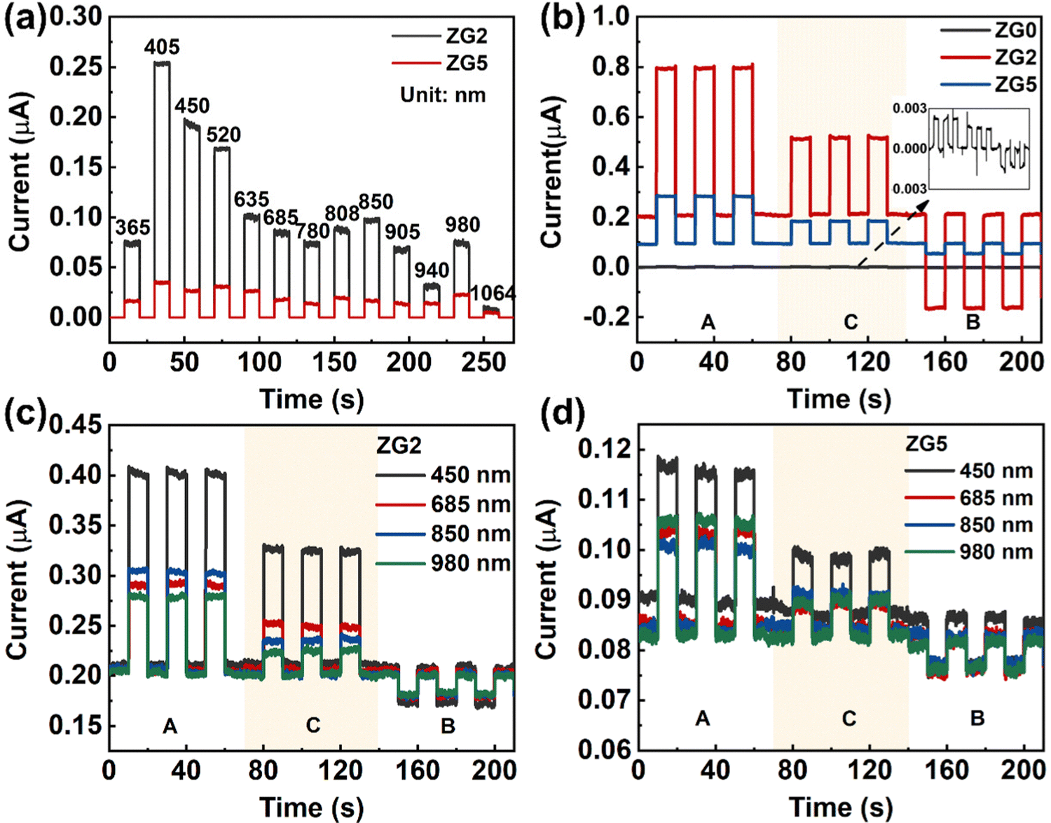 | ||
| Fig. 5 (a) I–t curves of ZG2 and ZG5 devices irradiated at different wavelengths (365–1064 nm) at zero bias. (b) I–t curves of ZG0, ZG2, and ZG5 devices illuminated at different positions using the light source (365 nm) at zero bias (inset is the enlarged view of the ZG0 device). (c) and (d) I–t curves of ZG2 and ZG5 devices at 450 nm, 685 nm, 850 nm, and 980 nm at zero bias. | ||
The incorporation of Ga atoms not only amplifies the PTE effect of ZnO but also extends it to the visible and near-infrared bands, as shown in Fig. 5c. The optical response curves of ZG2 and ZG5 at 450 nm, 685 nm, 850 nm, and 980 nm are given, at a constant power intensity of 5 mW cm−2. The results show that both ZG2 and ZG5 have PTE induced polarity reversal in the UV-Vis-NIR range, and ZG2 has the best optical response performance for each wavelength, which is believed to result from the LSPR of Ga doping. Herein, a self-powered doped ZnO photodetector is demonstrated, in which the photoresponse, detectivity and response speed of the device can be improved by Ga doping. An unprecedented ultra-wideband polarity reversal phenomenon is also revealed, which provides a new strategy for the development of ZnO based wide spectrum photodetectors.
Using different semiconductor materials to build heterostructures can often integrate the characteristics of the two materials and improve the optoelectronic properties of the materials. Therefore, we designed the BP NCs@GZO thin film heterojunction with the aim of further improving the optical response performance of the device. We combined the uniform dispersion of BP NCs prepared in the liquid phase with GZO thin film devices at various doping ratios. BZG0, BZG2, and BZG5 are the heterojunction photodetectors as shown in Fig. S3 (ESI†). The Ga doping ratios are 0%, 2%, and 5%, respectively. The light response curve of BZG under zero bias at 365 nm wavelength irradiation is shown in Fig. 6a. Compared with ZG devices in Fig. 4, the photocurrent of the BZG device increases significantly while the dark current decreases. This demonstrates that the semiconductor heterostructure formed by the assembly of BP NCs and ZG is beneficial in improving the device's optical response performance.
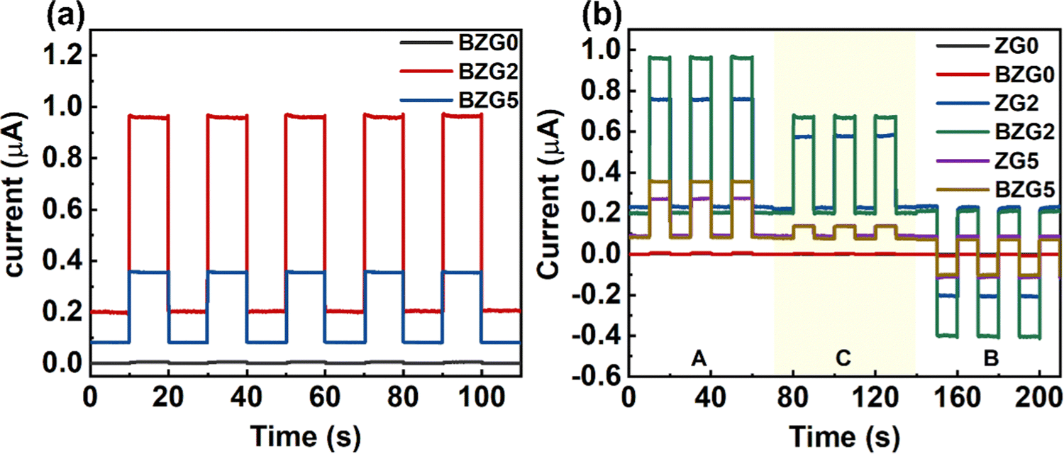 | ||
| Fig. 6 (a) I–t curves of different BP NCs@GZO devices at 365 nm. (b) I–t curves of ZG and BZG at different positions illuminated using a light source. | ||
BZG2 has the optimized detection ability for weak light, and the detection properties of BZG are improved compared with ZG, as show in Table 1. To verify the repeatability of the experiment, we tested another group of ZG and BZG. The results are shown in Fig. 6b, which shows the photoresponse curves of GZ and BZG at different positions of the light source. The results are consistent with what we discussed above It can be directly observed that the photocurrent of BZG is higher than that of ZG and has a lower dark current. After coupling BP NCs, the device also has a good PTE effect. According to the response speed results of BZG devices in Fig. 7, it can be seen that BZG2 has the fastest response speed, which can reach a τrise value of 1 ms and a τdecay value of 6.5 ms. Compared with GZO devices, it is found that the combination of BP NCs has greatly improved the response speed of the device.
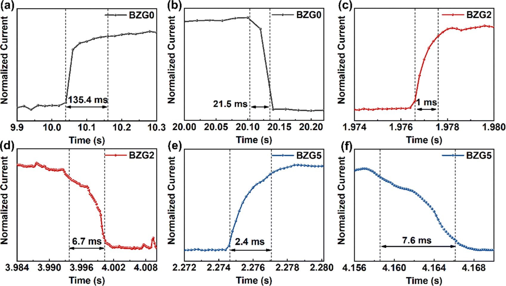 | ||
| Fig. 7 Rise and decay curves of BZG devices at 365 nm and zero bias. | ||
Conclusions
In conclusion, we demonstrate that ZnO based photodetectors show good self-powered performance in a wide UV-Vis-NIR (365–1064 nm) spectral range, which is believed to result from the LSPR introduced by Ga doping. An interesting current polarity reversal phenomenon is also observed owing to the PTE effects. In addition, the presence of BP NCs further improves the overall performance of photodetectors. BZG2 has a response of 12.86 mA W−1 and a detection of 2.295 × 10¹¹ Jones, and the rise and decay times are 1 ms and 6.7 ms, respectively. This work provides a promising method for fabricating wide-spectrum fast photodetectors taking advantage of the LSPR effect induced by noble-metal free, heavily doped semiconductors.Conflicts of interest
There are no conflicts to declare.Acknowledgements
This work was supported by the National Natural Science Foundation of China (Grant No. 52273298), the Guangdong Basic and Applied Basic Research Foundation (Grant No. 2022A1515010649), and the Shenzhen Science and Technology Program (Grant No. JCYJ20210324095611032, JCYJ20220818100008016 and JCYJ20220818100012025).References
- G. N. Ankah, P. Buchele, K. Poulsen, T. Rauch, S. F. Tedde, C. Gimmler, O. Schmidt and T. Kraus, Org. Electron., 2016, 33, 201 CrossRef CAS.
- Z. Ma, Y. Zhang, T. Li, X. Tang, H. Zhao, J. Li, C. Ma and J. Yao, Appl. Phys. A, 2020, 126, 869 CrossRef CAS.
- C. H. Kang, I. Dursun, G. Liu, L. Sinatra, X. Sun, M. Kong, J. Pan, P. Maity, E. N. Ooi, T. K. Ng, O. F. Mohammed, O. M. Bakr and B. S. Ooi, Light: Sci. Appl., 2019, 8, 94 CrossRef PubMed.
- H. Kind, H. Yan, B. Messer, M. Law and P. Yang, Adv. Mater., 2002, 14, 158 CrossRef CAS.
- J. S. Tyo, D. L. Goldstein, D. B. Chenault and J. A. Shaw, Appl. Opt., 2006, 45, 5453 CrossRef PubMed.
- T. Zhou, R. Zhang, X. G. Guo, Z. Y. Tan, Z. Chen, J. C. Cao and H. C. Liu, IEEE Photonics Technol. Lett., 2012, 24, 1109 CAS.
- Y. Audet, A. Bendali and J.-P. David, IEEE Trans. Electron Devices, 2021, 68, 1107 CAS.
- Y. J. Zeng, L. M. Pereira, M. Menghini, K. Temst, A. Vantomme, J. P. Locquet and C. Van Haesendonck, Nano Lett., 2012, 12, 666 CrossRef CAS PubMed.
- L. Hu, Q. Liao, Z. Xu, J. Yuan, Y. Ke, Y. Zhang, W. Zhang, G. P. Wang, S. Ruan, Y.-J. Zeng and S.-T. Han, ACS Photonics, 2019, 6, 886 CrossRef CAS.
- J. Jiang, J. Huang, Z. Ye, S. Ruan and Y. J. Zeng, Adv. Mater. Interfaces, 2020, 7, 2000882 CrossRef CAS.
- Y. Xin, L. Hu, S. Ruan, Z. Ye and Y.-J. Zeng, J. Mater. Chem. C, 2020, 8, 11399 RSC.
- J. Jiang, Y. Guo, X. Weng, F. Long, Y. Xin, Y. Lu, Z. Ye, S. Ruan and Y.-J. Zeng, J. Mater. Chem. C, 2021, 9, 4978 RSC.
- B. Deka Boruah and A. Misra, ACS Appl. Mater. Interfaces, 2016, 8, 18182 CrossRef CAS PubMed.
- B. D. Boruah and A. Misra, ACS Appl. Mater. Interfaces, 2016, 8, 4771 CrossRef PubMed.
- Y. J. Zeng, Z. Z. Ye, W. Z. Xu, D. Y. Li, J. G. Lu, L. P. Zhu and B. H. Zhao, Appl. Phys. Lett., 2006, 88, 062107 CrossRef.
- A. Agrawal, S. H. Cho, O. Zandi, S. Ghosh, R. W. Johns and D. J. Milliron, Chem. Rev., 2018, 118, 3121 CrossRef CAS PubMed.
- N. Pradhan, S. Das Adhikari, A. Nag and D. D. Sarma, Angew. Chem., Int. Ed., 2017, 56, 7038 CrossRef CAS PubMed.
- X. Ye, J. Fei, B. T. Diroll, T. Paik and C. B. Murray, J. Am. Chem. Soc., 2014, 136, 11680 CrossRef CAS PubMed.
- B. N. Pawar, S. R. Jadkar and M. G. Takwale, J. Phys. Chem. Solids, 2005, 66, 1779 CrossRef CAS.
- Y. S. No, D. H. Park, T. W. Kim, J. W. Choi, B. Angadi and W. K. Choi, Curr. Appl. Phys., 2012, 12, S71 CrossRef.
- K.-C. Lai, J.-H. Wang, C.-H. Lu, F.-J. Tsai, C.-H. Yeh and M.-P. Houng, Sol. Energ. Mat. Sol. C., 2011, 95, 415 CrossRef CAS.
- M. A. Lucio-López, A. Maldonado, R. Castanedo-Pérez, G. Torres-Delgado and M. D. L. L. Olvera, Sol. Energy Mater. Sol. Cells, 2006, 90, 2362 CrossRef.
- X. H. Yu, J. Ma, F. Ji, Y. H. Wang, X. J. Zhang, C. F. Cheng and H. L. Ma, J. Cryst. Growth, 2005, 274, 474 CrossRef CAS.
- Q. B. Ma, Z. Z. Ye, H. P. He, L. P. Zhu and B. H. Zhao, Mater. Sci. Semicond. Process., 2007, 10, 167 CrossRef CAS.
- K.-S. Ahn, Y. Yan, S. Shet, T. Deutsch, J. Turner and M. Al-Jassim, Appl. Phys. Lett., 2007, 91, 231909 CrossRef.
- S. Y. Jin, H. P. Gao, H. Zhang, F. Xu, Y. Sun, W. W. You, G. C. Pan, H. F. Zhang, Z. L. Zhang and Y. L. Mao, Ceram. Int., 2021, 47, 26025 CrossRef CAS.
- B. Zhang, J. Luo, Z. Chen, L. T. Wu, J. Q. Li, Y. Y. Tian and S. L. Liu, J. Electroanal. Chem., 2022, 918, 10 Search PubMed.
- X. G. Ding, C. H. Liow, M. X. Zhang, R. J. Huang, C. Y. Li, H. Shen, M. Y. Liu, Y. Zou, N. Gao, Z. J. Zhang, Y. G. Li, Q. B. Wang, S. Z. Li and J. Jiang, J. Am. Chem. Soc., 2014, 136, 15684 CrossRef CAS PubMed.
- G. H. He, M. M. Jiang, L. Dong, Z. Z. Zhang, B. H. Li, C. X. Shan and D. Z. Shen, J. Mater. Chem. C, 2017, 5, 2542 RSC.
- Z. P. Sun, M. M. Jiang, W. Q. Mao, C. X. Kan, C. X. Shan and D. Z. Shen, Photonics Res., 2020, 8, 91 CrossRef CAS.
- X. Wen, Q. Zhang and Z. Shao, Crystals, 2019, 9, 263 CrossRef CAS.
- E. D. Bourret-Courchesne, S. E. Derenzo and M. J. Weber, Nucl. Instrum. Methods Phys. Res., Sect. A, 2009, 601, 358 CrossRef CAS.
- A. L. Zhao, H. Li, X. J. Hu, C. Wang, H. Zhang, J. G. Lu, S. C. Ruan and Y. J. Zeng, J. Phys. D: Appl. Phys., 2020, 53, 293002 CrossRef CAS.
- Z. H. Ling, P. Li, S. Y. Zhang, N. Arif and Y. J. Zeng, J. Phys. Condens. Matter, 2022, 34, 224004 CrossRef CAS PubMed.
- J. Yuan, L. Hu, Z. Xu, Y. Zhang, H. Li, X. Cao, H. Liang, S. Ruan and Y.-J. Zeng, J. Phys. Chem. C, 2019, 123, 14766 CrossRef CAS.
- A. K. Zak, N. S. Abd Aziz, A. M. Hashim and F. Kordi, Ceram. Int., 2016, 42, 13605 CrossRef.
- D. R. Sahu, S. Y. Lin and J. L. Huang, Microelectron. J., 2007, 38, 245 CrossRef CAS.
- F. Leiter, H. Alves, D. Pfisterer, N. G. Romanov, D. M. Hofmann and B. K. Meyer, Physica B, 2003, 340, 201 CrossRef.
- A. Boltasseva and H. A. Atwater, Science, 2011, 331, 290 CrossRef CAS PubMed.
- F. C. Correia, N. Bundaleski, O. Teodoro, M. R. Correia, L. Rebouta, A. Mendes and C. J. Tavares, Appl. Surf. Sci., 2018, 458, 1043 CrossRef CAS.
- U. Ozgur, Y. I. Alivov, C. Liu, A. Teke, M. A. Reshchikov, S. Dogan, V. Avrutin, S. J. Cho and H. Morkoc, J. Appl. Phys., 2005, 98, 103 CrossRef.
- L. Hu, J. Yuan, Y. Ren, Y. Wang, J. Q. Yang, Y. Zhou, Y. J. Zeng, S. T. Han and S. Ruan, Adv. Mater., 2018, 30, 1801232 CrossRef PubMed.
- Z. Xu, L. Hu, J. Yuan, Y. Zhang, Y. Guo, Z. Jin, F. Long, Y. Long, H. Liang, S. Ruan and Y. J. Zeng, Adv. Mater. Interfaces, 2020, 7, 1902075 CrossRef CAS.
- F. Wang, Z. Wang, L. Yin, R. Cheng, J. Wang, Y. Wen, T. A. Shifa, F. Wang, Y. Zhang, X. Zhan and J. He, Chem. Soc. Rev., 2018, 47, 6296 RSC.
- L. Shi, K. Chen, A. Zhai, G. Li, M. Fan, Y. Hao, F. Zhu, H. Zhang and Y. Cui, Laser Photonics Rev., 2020, 15, 2000401 CrossRef.
- X. Lu, L. Sun, P. Jiang and X. Bao, Adv. Mater., 2019, 31, 1902044 CrossRef CAS PubMed.
- M. Buscema, M. Barkelid, V. Zwiller, H. S. J. van der Zant, G. A. Steele and A. Castellanos-Gomez, Nano Lett., 2013, 13, 358 CrossRef CAS PubMed.
- Y. Guo, Y. Song, M. Yang, Z. Xu, H. Xie, H. Li, Z. Li, H. Liang, S. Ruan and Y.-J. Zeng, J. Mater. Chem. C, 2020, 8, 13226 RSC.
Footnotes |
| † Electronic supplementary information (ESI) available. See DOI: https://doi.org/10.1039/d3ma00017f |
| ‡ Manli Yang and Xiaoliang Weng contributed equally to this work. |
| This journal is © The Royal Society of Chemistry 2023 |