DOI:
10.1039/D2MA00962E
(Paper)
Mater. Adv., 2023,
4, 1062-1074
Photocurrent conversion capability of a 2D WS2-polyvinyl alcohol matrix and its DFT-based charge carrier dynamics analysis†
Received
9th October 2022
, Accepted 4th January 2023
First published on 18th January 2023
Abstract
In the present research article, we have studied the photodetection mechanism of WS2 nanosheets embedded in a polyvinyl alcohol matrix. Hydrothermally synthesized nanosheets of WS2 were embedded in a polyvinyl alcohol (PVOH) matrix by the solution method. The SEM micrographs show the clear incorporation of WS2 nanosheets in the PVOH matrix. XRD results reveal the hexagonal-type crystal structure of the WS2 nanosheets with the space group of P63/mmc. A Tauc plot of the UV-Visible absorption spectrum of the WS2 PVOH matrix shows the optical band gap energy of 3.51 eV, which is intermediate between those of the WS2 nanosheets and PVOH matrix. The zeta potentials of the WS2 nanosheets, PVOH and WS2 PVOH were found to be −10.60 mV, −4.14 mV and −1.12 mV, respectively. The responsivity and detectivity were found to be 369.13 mA W−1 and 5.25 × 10¹¹ Jones, respectively, in the photodetection measurement for the WS2 PVOH metallopolymer. The density functional studies show that upon the incorporation of the WS2 nanosheets into the PVOH matrix, the HOMO–LUMO energy gap significantly decreases. Electronic properties such as electron affinity, ionization potential, chemical hardness, and amount of charge transfer concluded based on DFT also support the experimental results.
1. Introduction
Photon to electricity conversion materials are employed in any application that calls for the detection of light at a specific wavelength, including imaging, spectroscopy, remote sensing, solar cells and others.1,2 The great majority of silicon based photodetectors currently in use, operate in the visible or near-infrared region and have peak operating wavelengths greater than 500 nm. Wide ranges of mechanical, electrical, and optoelectronic characteristics of two-dimensional materials, including transition metal dichalcogenides (TMDCs), are currently the subject of intense research. The 2D material that has received the greatest attention is graphene, which led to the field's expansion to other 2D materials including TMDCs.3–5 Next-generation devices can function more effectively due to the special properties of 2D materials, including their ultrathin planar structure, strong electron–hole confinement, and layer-dependent variable bandgap. These characteristics make it possible to create devices that are smaller, more flexible, and more efficient.6–8 In graphene, the absence of a band gap, despite its exceptional carrier mobility, restricts its use in electronics. Due to their unique features, TMDCs have received a lot of interest and have been suggested as prospective candidate for photonic and optoelectronic devices.9–11
In contrast to other two-dimensional materials, WS2 demonstrates unique characteristics including conductivity, which makes it ideal for contacts and interconnections, mechanical strength, a very high elastic modulus, high thermal stability, and excellent mobility. Graphene is the most researched two-dimensional material.12–14 The ability to directly fabricate heterojunctions made up of several 2D materials is made possible by the same weak van der Waals interactions that make it simple to separate atomically thin sheets from stacked solids.15–19 The next generation of optoelectronic and nanoscale electronic devices will be built using heterostructures based on these TMDCs.20,21 2D materials may be coupled with other electronic materials including zero-dimensional quantum dots (0D), one-dimensional nanotubes (1D), and polymers (3D) to create mixed-dimensional van der Waals (vdW) heterostructures with new device properties.22–24 Numerous studies have also been done on certain other characteristics, such as transparency, stretchability, and self-healing.25,26
Polymer materials are potential materials for a new generation of photodetectors because of their inherent flexibility, solution processability, large-area preparation, and tunable molecular structure. This is accomplished by various molecular design methodologies and novel device designs.27 Thick-film photoactive layers are preferred in all-polymer photodetectors to obtain high detectivity since they can efficiently reduce the dark current density. However, if the photoactive layer of the film is too thick, it causes greater recombination loss, which reduces responsiveness.28,29 Impact ionization cannot happen in organic photodetectors like in inorganic avalanche photodiodes because the exciton binding energy of organic semiconductor materials is roughly 0.1–1.4 eV, which is three orders higher than that of inorganic semiconductor materials28 and trap-assisted carrier tunneling effects have been primarily responsible for helping to identify the working mechanism of organic photodetectors.30 In this research, the photo to current conversion capability is tested in terms of the performance parameters such as responsivity (R), detectivity (D), external quantum efficiency (EQE), linear dynamic range (LDR), and noise equivalent power (NEP). Due to the presence of the W atom in the WS2 and the –OH functional group in the PVOH matrix, in the metallopolymeric system, there is an interaction between them. This is also studied by the density functional theory approach for insight into the charge carrier dynamics.
2. Experimental section
2.1 Materials used
Sodium tungstate dihydrate (Na2WO4·2H2O, Fisher Scientific, >99.5%), thiourea (NH2CSNH2, SDFCL, >99), polyvinyl alcohol (Sigma Aldrich, >99.9%), N-methyl-2-pyrrolidone [C5H9NO, Merck, >99.3%], ethanol [C2H5OH], and acetone [CH3COCH3] of Fisher Scientific India.
2.2 Synthesis of 2D WS2 nanosheets
In a typical synthesis technique, 30 mL of double-distilled water was used to make a 0.3 M solution of sodium tungstate dihydrate, which was then stirred for 1 hour at 90 °C. Following that, a 0.6 M solution of thiourea was prepared in 30 mL of double-distilled water. The thiourea solution was then added to a tungsten precursor solution and the mixture was again stirred at 150 °C for 3 hours at a speed of 500 rpm (relation (1b)). The mixture was then cooled to room temperature and titrated with HCl while being constantly stirred until a brown precipitate developed. The final pH was adjusted to 1 because at this pH value most of the material precipitated. Then, this solution was put into a 100 mL autoclave that was lined with Teflon. The autoclave was placed in an oven set at 150 °C for 5 hours. This solution was removed from the oven after natural cooling and centrifuged three times at 3500 rpm with distilled water. Additionally, this powder was dried in a programmable oven at 200 °C (relation (1c)).| | | (NH2)2CS + 2H2O → 2NH3 + CO2 + H2S | (1a) |
| | | Na2WO4·2H2O + 3H2S → WS3 + 2NaOH + 4H2O | (1b) |
2.3 Incorporation of WS2 nanosheets into the PVOH matrix
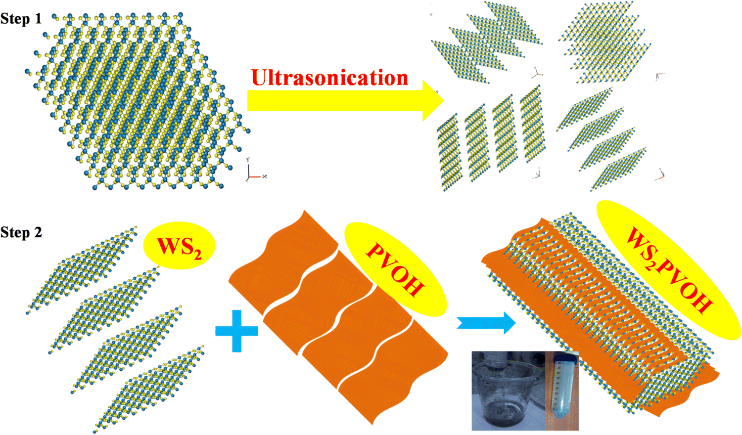
In the first step of the synthesis, WS2 was dissolved in N-methyl pyrrolidone and ultra-sonicated for 5 hours in an ultrasonic bath for further breaking the WS2 sheets into smaller sheets, as shown in Fig. 1 (step 1). After ultra-sonication, these WS2 nanosheets were centrifuged at 3500 rpm to collect them. These bottom collected WS2 nanosheets were dried at 80 °C in a programmable oven. The process of incorporation of WS2 sheets into the PVOH matrix is depicted in Fig. 1 (step 2). In 50 mL of double distilled water 5 g of polyvinyl alcohol was dissolved at 80 °C on a magnetic stirrer. When all the PVOH dissolved in distilled water 1 g of previously synthesized WS2 nanosheets was dropped into the PVOH solution and this solution was continuously stirred up to 5 hours. This WS2 nanosheet embedded PVOH matrix was used for further analysis.
 |
| | Fig. 1 Preparation procedure for the WS2 PVOH metallopolymer. | |
3. Results and discussion
3.1 Surface morphological investigation
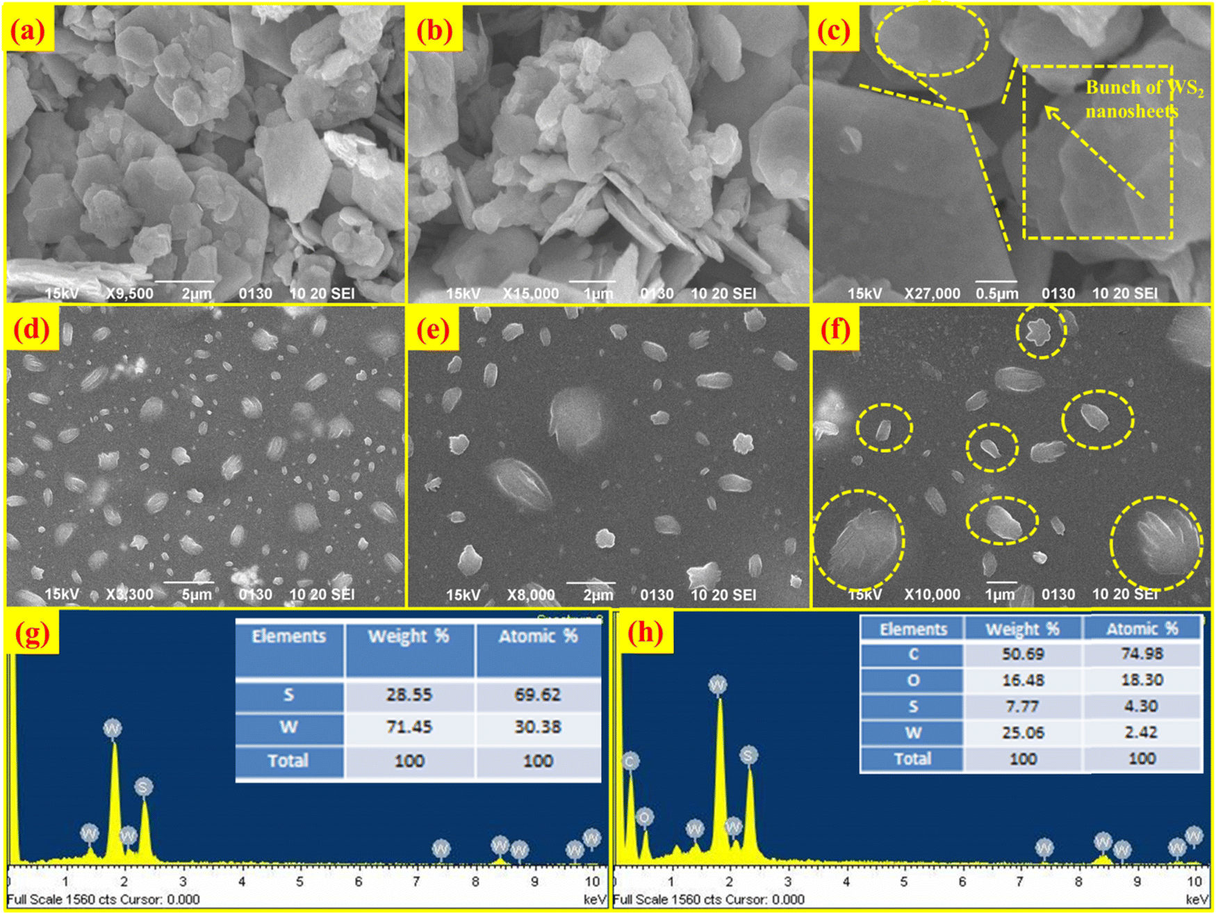
Scanning electron microscopy (SEM) was used to examine the morphology of the samples. Fig. 2(a–c) displays the SEM pictures of the WS2 hexagonal nanosheets. It is evident from Fig. 2(b) and (c) that there are several clusters of nanosheets, whereas Fig. 2(c) clearly shows hexagon-shaped sheets. It can be seen that nanosheets incorporated in the PVOH matrix are essentially monodispersed, loosely stacked, and have a width between 100 and 500 nm and a thickness of 10 nm. Energy dispersive X-ray spectroscopy (EDS) was used to confirm the elemental composition of the as-prepared materials. In the EDS spectrum of WS2, W and S elements are observed with an atomic percentage of 30.38 and 69.62% respectively, as shown in Fig. 2(g). In the WS2 PVOH matrix, W and S were found to be 2.42% and 4.30% whereas C and O are also present with an atomic percentage of 74.98% and 18.30%, respectively, as depicted in Fig. 2(h).
 |
| | Fig. 2 Scanning electron micrographs of WS2 nanosheets at (a) 2 μm, (b) 1 μm and (c) 0.5 μm, scanning electron micrographs of WS2 nanosheets embedded in a PVOH matrix at (d) 5 μm, (e) 2 μm and (f) 1 μm, (g) EDS spectrum of WS2 nanosheets and (h) EDS spectrum of WS2 PVOH. | |
3.2 Raman spectroscopic analysis
Raman spectroscopy is frequently used to ascertain the number of layers and other important characteristics of layered 2D materials. The point group corresponds to D6h for bulk, D3h for an odd number of layers, and D3d for an even number of layers.31 The crystal structure of 2H-WS2 belongs to the D6h4 point group. The following relation (2) describes the zone center phonons’ irreducible representations.32| | | Γ = A1g + 2A2u + B1u + 2B2g + E1g + 2E1u + E2u + 2E2g | (2) |
The E2g1 mode involves in-plane displacement of transition metal and chalcogen atoms, whereas the A1g mode only involves chalcogen atoms and is an out-of-plane vibration.33 E2g2 is a shear mode that manifests at very low frequencies and describes the vibration of two stiff layers rubbing against one another. The back-scattering Raman setup forbids the E1g mode, an in-plane vibration of solely the chalcogen atoms.33,34Table 1 demonstrates how the peaks are shifting. The strongest second-order Raman peak, the 2LA(M) mode at 350.718 cm−1, is nearly twice as strong as the first-order A1g(Γ) such as shown in Fig. 3(a). However, at 358.924 cm−1, the second-order 2LA(M) mode overlaps with the first-order E12g(Γ) mode.
Table 1 Raman modes in WS2 nanosheets and WS2 PVOH
| S. no. |
WS2 nanosheets (cm−1) |
WS2 PVOH (cm−1) |
Δω (cm−1) |
| 1. |
299.089 |
300.712 |
1.623 |
| 2. |
332.619 |
332.975 |
0.356 |
| 3. |
350.718 |
351.880 |
1.162 |
| 4. |
358.924 |
359.851 |
0.927 |
| 5. |
423.748 |
424.414 |
0.666 |
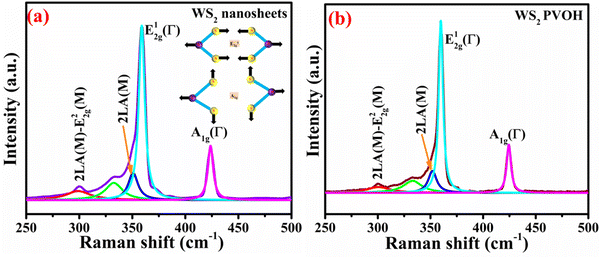 |
| | Fig. 3 (a) Raman spectrum of WS2 nanosheets (inset: Raman modes). (b) Raman spectrum of WS2 PVOH. | |
3.3 Structural analysis
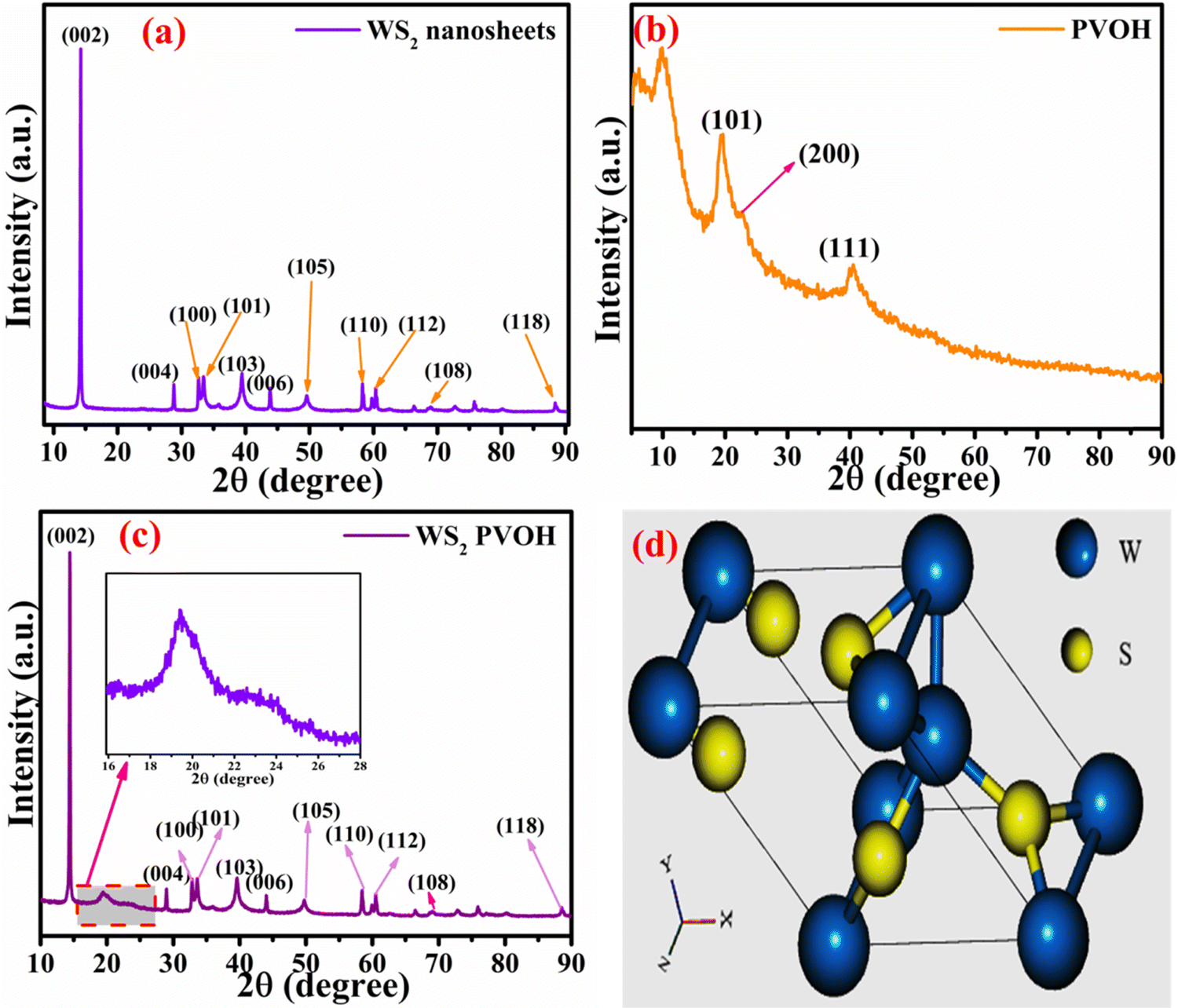
To evaluate the structure, these nanomaterials were analyzed by X-ray diffraction (XRD) technique. The XRD pattern of the WS2 nanosheets is shown in Fig. 4(a), with the (hkl) planes of (002), (004), (100), (101), (103), (006), (105), (110), (112), (108) and (118) found at the 2θ angles of 14.22°, 28.79°, 32.66°, 33.42°, 39.43°, 43.85°, 49.59°, 58.32°, 60.39°, 68.91° and 88.42°, respectively. In the diffraction pattern of PVOH as in Fig. 4(b), the diffraction peaks at 19.57°, 22.74° and 40.52° correspond to the (101), (200) and (111) reflection planes. This crystalline peak of PVOH is also similar to some previous results.35 The –OH group contributes to the crystallinity of PVOH, a semi-crystalline polymer. These crystalline areas, which are dispersed randomly throughout the polymer, are crucial to the polymer's chemical and physical characteristics. The XRD pattern of PVOH is distinguished by the chains in a trans-planar conformation packed in a monoclinic unit cell, according to the PVOH's diffraction profile.36 The PVOH main chain has enough –OH groups to create potent intra- and intermolecular hydrogen bonds. Because of its high crystallinity, WS2 is extremely dominating in the overall pattern, as seen by the XRD pattern of WS2 PVOH in Fig. 4(c). The Scherrer formula (relation (3)) was used to compute the average crystallite size.| |  | (3) |
where k is the Scherrer constant, β is the full width and half maximum, and Cu kα is the wavelength (λ = 0.15406 nm). The WS2 nanosheets’ average crystallite size was found to be 32.40 nm.
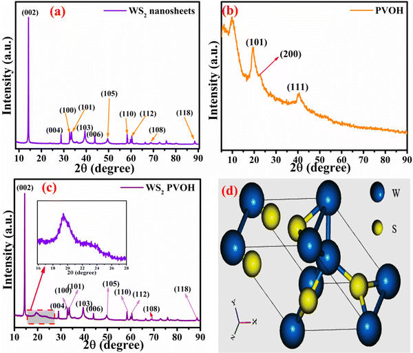 |
| | Fig. 4 X-Ray diffraction pattern of (a) WS2 nanosheets, (b) PVOH and (c) WS2 PVOH. (d) Crystal unit cell of WS2. | |
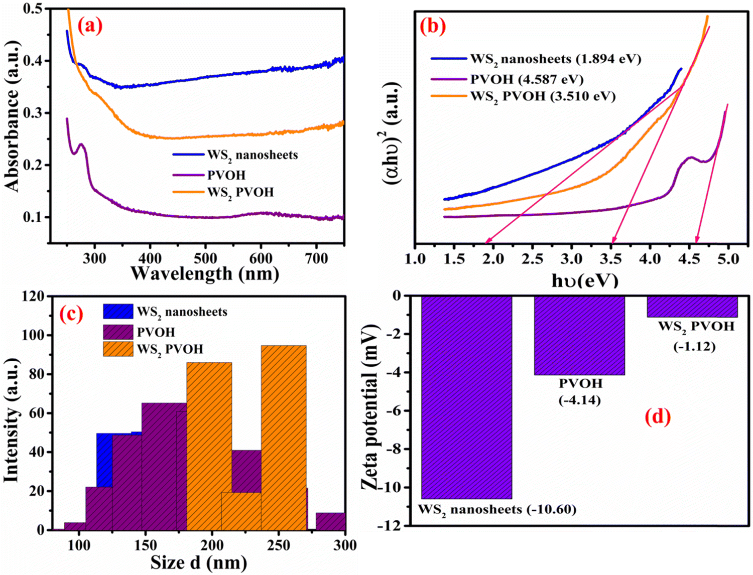
3.4 UV-Visible absorption spectroscopy
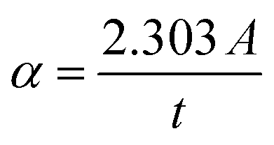
The UV-Visible absorption spectra for WS2 nanoflakes, PVOH, and WS2 PVOH are shown in Fig. 5(a) in the range of 200 to 750 nm. The absorption coefficient of all samples was calculated by the Beer–Lambert law such as given in relations (4) and (5).| |  | (5) |
where I and I0 are the optical intensities at the moment and the initial intensity, α is the absorption coefficient, t is the cuvette's thickness, and A is the absorption. The Tauc plot technique was used to determine the optical band gap energy of the materials, and it is presented in relation (6).The exponent n is used to express the type of band transition, where n = 2 and 3 respectively denote indirect permitted and indirect forbidden transitions, while n = 1/2 and 3/2 respectively denote direct permitted and direct prohibited transitions, A is a constant and ν denotes the transition frequency. The optical band gap was found by projecting the straight line segment of the (αhν)2 against hυ curves to zero.37,38 The predicted band gaps of the as-prepared materials were determined to be 1.94 eV for WS2 nanosheets and 4.51 eV for PVOH, whereas 3.51 eV for WS2 PVOH as shown in Fig. 5(b).
 |
| | Fig. 5 (a) UV-Visible absorption spectrum of WS2 nanosheets, PVOH and WS2 PVOH. (b) Tauc plot for WS2 nanosheets, PVOH and WS2 PVOH. (c) Dynamic light scattering spectrum of WS2 nanosheets, PVOH and WS2 PVOH. (d) Zeta potential plot for WS2 nanosheets, PVOH and WS2 PVOH. | |
3.5 Dynamic light scattering analysis
When suspended in a liquid, nanoparticles scatter light in a manner proportional to the sixth power of their radii.39 When using DLS, the autocorrelation function is calculated using the mono-exponential relation (7) and the variations in scattered light intensity are correlated against short decay periods.40,41where q is the scattering vector, Dt is the translational diffusion coefficient, and b is an instrument-dependent constant. The Stokes–Einstein relation (8) links this translational diffusion coefficient to the hydrodynamic radius (RH) of solid spherical particles.42| |  | (8) |
From the analysis of the as-prepared materials, the distribution of nanoparticles is presented in Fig. 5(c). However, in PVOH, this size distribution is dominated in a wide range between 70 and 300 nm. The distribution of WS2 nanosheets was found to be 100–200 nm. The WS2 PVOH material's particle size distribution lies between these two counterparts which is in the range of 175–275 nm.
3.6 Zeta potential analysis
The electrified double layer of electrophoretically movable particles and the layer of dispersant around them have a potential difference at the sliding plane known as the zeta potential. Zeta potential measurements are highly associated with the colloid's stability. Zeta potential levels are categorized as very unstable, generally stable, moderately stable, and highly stable, respectively, between the ranges of 0–10 mV, 10–20 mV, 20–30 mV, and 30 mV.42,43 The WS2 nanosheets’ zeta potential value discovered to be −10.60 mV, showing that they are relatively stable in their solvent, as opposed to PVOH and WS2 PVOH, whose zeta values were detected to be −4.14 mV and −1.12 mV and displayed in Fig. 5(d). These two dispersant solutions are very unstable, as shown by Fig. 5(d), which indicates that they have a tendency to aggregate.
3.7 Photodetection analysis and their mechanism
Fig. 6 displays the schematic representation of the photodetection measurement set-up, which consists of a light source of the wavelength centered at 365 nm. This setup is connected with an electrometer and the computer through the GPIB port. The band diagram presented in Fig. 6 shows that under the ambient atmospheric conditions, oxygen molecules adsorbed on the surface of the materials in the form of O2−, taking an electron from the conduction band. Thus a depletion region is formed between the material and oxygen species. Upon illumination these oxygen species are removed from the surface of the materials, so the depletion width is reduced and a higher level of photocurrent is observed. In the photoconduction process, instead oxygen adsorption/desorption mechanisms along with exciton generation, transportation and collection are also responsible. Such as under illumination, electron–hole pairs are generated in the materials and under the application of small potential drift these excitons move towards the respective electrodes and are collected on the electrodes, which is exhibited as increased photocurrent in the external circuit. Our photodetector devices have a metal–semiconductor–metal (MSM)-based coplanar device structure, where silver (Ag) is used for symmetrical electrodes. There is a need to enhance photodetector performance parameters such as responsivity, detectivity, noise equivalent power and external quantum efficiency because their usability in diverse fields needs different specifications. For more accurate and precise measurements of light, a highly responsive photodetector must be chosen, whereas for the detection of weak light signals, a high detectivity and low NEP photodetector device is needed. There are two approaches to increase the sensitivity of photodetectors: by improving the external quantum efficiency and by reducing the dark current density. One of the most crucial methods for increasing EQE and producing high-sensitivity photodetection is the photomultiplication (PM) effect.44 Since the exciton binding energies of organic semiconductor materials are in between 0.1 and 1.4 eV, and are roughly three orders more than those of inorganic semiconductors, impact ionization cannot take place in organic photomultiplication as it can in inorganic photodiodes. Instead, carrier tunneling events facilitated by traps have been used to investigate how organic PM photodetectors operate.28,45 The EQE of the majority of organic MSM photodetectors is substantially higher than 100% owing to the carrier tunneling effect that is helped by traps.46,47 When the Fermi energy level of the metal electrode is higher than that of the hybrid material, the required Schottky band bending without bias occurred in organic-inorganic semiconductors with a lot of electron traps.28,48 Ag, Al, and Mg electrodes must be used to create band bending because of their low work functions. Photo-generated electrons are captured by electron traps when exposed to light and travel toward the Schottky junction in the presence of a biased electric field from the electrode to the semiconductor.28,49 As a result of the incoming electrons narrowing the Schottky junction there and boosting the internal electric field's strength, holes are then able to tunnel through the junction and inject into the hybrid semiconductor from the outside circuit, resulting in current multiplication.50 A high-frequency detector that uses an insulating layer to exclude ambient light has recently been developed in photodetectors. The narrowband detector requirement is a further invention that uses ineffective charge transport to produce a sizable peak in external quantum efficiency near the optical absorption edge of active layers.51 Different material-based photodetector devices are presented in Table 2 for the comparison of these results. The linear Ohmic properties are shown in Fig. 7(a–c), which denotes the emergence of Ohmic connections between the material and electrodes. The photodetector device based on WS2 PVOH shows a high photocurrent but at the same time is less effective towards the intensity, which may be due to the presence of WS2 traps in the PVOH matrix. According to Fig. 7(d), it is also evident that WS2 PVOH exhibits a higher photocurrent than pure WS2 nanosheets and PVOH.
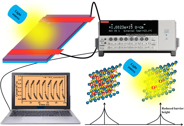 |
| | Fig. 6 The experimental set-up is depicted schematically, along with the corresponding band diagram under dark and illuminated conditions. | |
Table 2 Different materials-based photodetector devices
| Material |
R (A W−1) |
D (Jones) |
P
inc (μW cm−2) |
EQE (%) |
Ref. |
| WS2–PVOH |
0.36 |
5.25 × 10¹¹ |
50 |
125.15 |
Present work |
| PVA/CQD |
0.267 |
— |
5 × 10³ |
158 |
54
|
| Polyaniline–WSe2 |
0.017 |
1.11 × 10¹⁰ |
1 × 10⁴ |
— |
56
|
| CuPc/BPPC |
0.008 |
3.94 × 10⁹ |
1 × 10⁵ |
3.92 |
57
|
| MoS2-PAM |
0.60 |
4.96 × 10¹¹ |
4 × 10⁴ |
20.37 |
58
|
| Ga2O3-EAP |
3.1 |
1.42 × 10¹¹ |
31 |
4.5 × 10⁴ |
59
|
| Pentacene/C60 |
0.025 |
2.0 × 10¹⁰ |
1 × 10⁵ |
5 |
60
|
| Cs3Bi2I9 |
0.003 |
1.6 × 10¹² |
100 |
— |
61
|
| CQD/ZnO |
0.14 |
8.33 × 10¹² |
1 × 10³ |
— |
62
|
| Polyaniline–ZnO |
0.024 |
— |
9.3 × 10² |
7.47 |
63
|
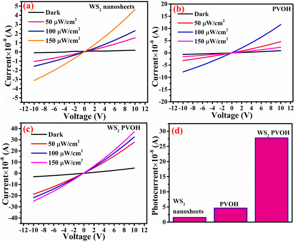 |
| | Fig. 7 Current–voltage characteristics of (a) WS2 nanosheets, (b) PVOH and (c) WS2 PVOH. (d) Comparison of the photocurrent in WS2, PVOH and WS2 PVOH at 10 V under an illumination intensity of 50 μW cm−2. | |
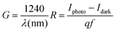
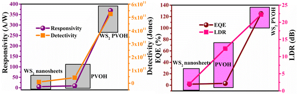
Fig. 8 displays the transient photoresponse behavior of all the as-prepared devices. From Fig. 8(a) the transient photoresponse of the WS2 nanosheets exhibited a very fast and stable photoresponse, which is attributed to the two-dimensional nature with lower recombination centers. Whereas the photoresponse of WS2 PVOH shows some level of enhancement in the current after some on/off cycles; the main reason behind this is that after interaction with light some thermally excited carriers were also generated, which contributed to the photocurrent but at the same time reduced the stability of the device. The WS2 PVOH device was also checked for long term stability up to 600 s such as presented in Fig. 8(d), which also exhibits the fluctuating nature of the device where after some time, the current decreases and then increases within some threshold limit. This degrading behavior of the device was also confirmed by the photodetection measurement of the pure PVOH device as shown in Fig. 8(f), which exhibited that after each measurement the photocurrent degraded, which is attributed to the fact that PHOV is more thermally responsive as compared to photons, whereas WS2 nanosheets are photoresponsive. Upon combining these two materials we found a photodetector device, with high photocurrent and long-term stability. Relation (9) defines the responsivity of the photodetector device as the production of photocurrent from the noise level for each incident photon per unit area.52,53 The calculated responsivity of the photodetector devices is found to be 5.24 mA W−1 and 9.22 mA W−1 for WS2 nanosheets and PVOH, respectively, whereas the responsivity for the WS2 PVOH nanohybrid was significantly enhanced and found to be 369.13 mA W−1, which is due to the fact that upon incorporating the WS2 sheets into the PVOH matrix, the photocurrent rises at lower potentials. This result is very close to the previously reported PVA/CQD-based device responsivity of 0.26 A W−1.54 According to relation (10), the gain of a photoconductor is equal to the minority carrier recombination lifetime divided by the time the carriers need to travel across the semiconductor between the two contacts of the device. Given that the transit time is significantly less than the recombination lifetime, a photoconductor will inevitably experience a considerable gain. The photogenerated carriers have numerous opportunities to go through the circuit before recombination because of the short transit time, which results in many times more photoexcited carriers. This is how the gain physically explains itself. The gain for the WS2 PVOH device is 1.25 × 10⁹, which is significantly higher than the gain of WS2 of 1.78 × 10⁷ and PVOH of 3.13 × 10⁷, indicating that more carriers are collected at the electrodes in the material WS2 PVOH.
| |  | (9) |
| |  | (10) |
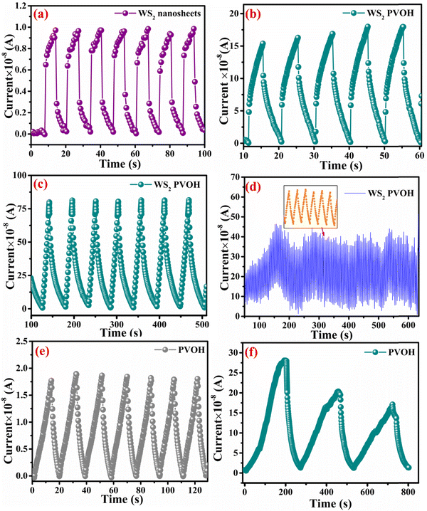 |
| | Fig. 8 (a) Transient photoresponse of WS2 nanosheets. (b) Transient photoresponse of WS2 PVOH with a small duration illumination pulse. (c) Transient photoresponse of WS2 PVOH for a large duration illumination pulse. (d) Stability of the WS2 PVOH photodetector device over 600 s. (e) Transient photoresponse of PVOH. (f) Transient photoresponse of PVOH for a large duration illumination pulse. | |
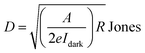
A photodetector's operation and properties can be determined by looking at its external quantum efficiency and detectivity characteristics. In contrast, detectivity describes the capacity of the photodetector to detect weak signals and can be calculated by relation (12). The collected charge carriers at the electrodes for each incoming photon are referred to as EQE (relation (11)).55 The EQE values for the PVOH and WS2 are found to be 3.12% and 1.77% but for the WS2 PVOH device, it was observed to be 125.15%, which is much higher than that of both of its constituent parts, and as shown in Fig. 9(b), the EQE is higher than 100% indicating the photomultiplication phenomena in the WS2 PVOH material.
| |  | (11) |
| |  | (12) |
 |
| | Fig. 9 (a) Responsivity and detectivity of the WS2 PVOH photodetector device. (b) EQE and LDR of the WS2 PVOH photodetector device. | |
In contrast to noise equivalent power, which is defined as the observable optical power from its noise level, linear dynamic range (relation (13)) refers to the range of photodetector response to the input light. The LDR values for WS2 nanosheets, PVOH and WS2 PVOH are observed to be 2.07 dB, 12.32 dB and 22.259 dB, respectively. Noise equivalent power (relation (14)) for WS2 PVOH is observed to be 1.67 × 10⁻⁷ W, which is much lower than that of both of its constituents, which means that it can detect much low optical signals than WS2 nanosheets and PVOH. For the photodetector device, the response and recovery times are also crucial and are calculated by fitting relations (15) and (16). The response and recovery times for the WS2 PVOH devices were found to be 1.158 s and 1.868 s, respectively, whereas the response and recovery times for WS2 nanosheets were found to be the best as shown in Fig. 10(a).
| |  | (13) |
| |  | (14) |
| | | I(t) = Idark(1−e−t/τd) | (16) |
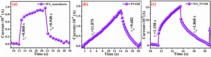 |
| | Fig. 10 Rise and decay time constants for (a) WS2 nanosheets, (b) PVOH and (c) WS2PVOH. | |
3.8 Density functional theory (DFT) approach
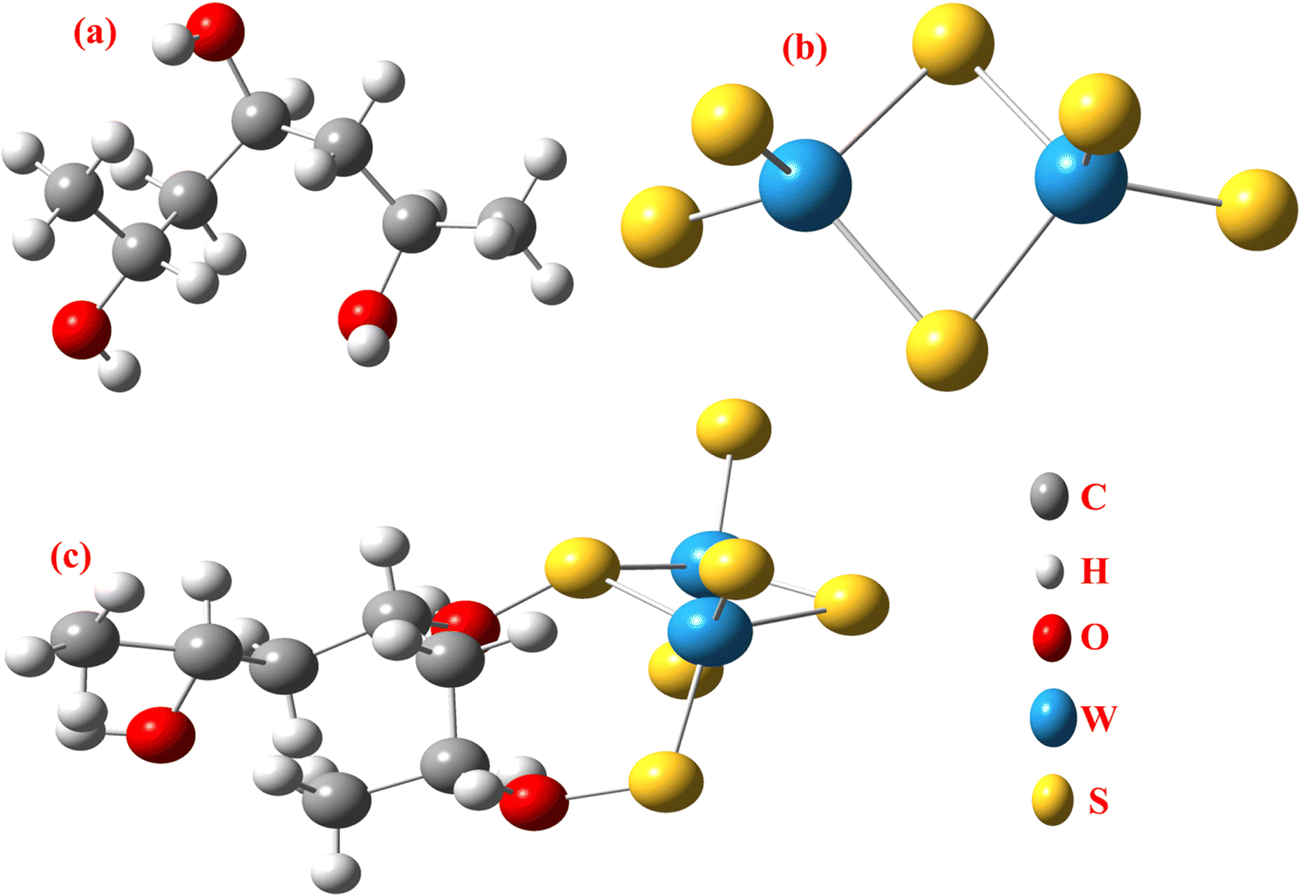
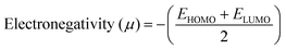
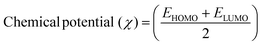
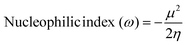
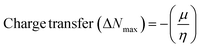
The DFT results are obtained by the simulation of PVOH, WS2 and WS2 PVOH. The molecules were created by using Gauss View 05 and the Gaussian 09 program was used for the DFT calculations. The basis set of LanL2DZ was employed in this optimization process together with the ground state B3LYP density functional theory model.64,65 The optimized structures of PVOH, WS2 and WS2 PVOH are presented in Fig. 11. Ning Xu et al.66 also showed that the metallopolymer of WS2 PVOH looks yellowish green, and is smooth with no obvious defects and excellent transparency. Certain S bare atoms that appeared at the edges of the nanosheets and could easily interact increased the force between PVOH and WS2. On the other hand, the WS2 addition disrupted the regularity of the PVOH polymer array. Evident improvement has been made in the composite's temperature properties, primarily because the physical barrier provided by the nanosheets can limit the thermal mobility of the polymer chain and inhibit heat conduction. These exposed S atoms produced a strong contact with the PVOH molecular chain, delaying the thermal breakdown of the composite material.66 In the metallopolymeric system, there is contact between them because the W atom is in the WS2 and the –OH functional group is in the PVOH matrix. There are certain electronic parameters, such as HOMO–LUMO gap (ΔE), electron affinity (EA), ionization potential (IP), electronegativity (μ), chemical potential (χ), chemical hardness (η), chemical softness (σ), and nucleophilicity index (ω), which can be calculated by relations (17)–(24),67–69 to investigate the properties of the metallopolymeric system as presented in Table 3.
 |
| | Fig. 11 Optimized structure of (a) PVOH, (b) WS2 and (c) WS2 PVOH. | |
Table 3 Electronic parameters of the simulation results
| Materials |
E
HOMO (eV) |
E
LUMO (eV) |
Band gap (eV) |
Electron affinity (eV) |
Ionization potential (eV) |
Electronegativity (eV) |
Chemical potential (eV) |
Chemical hardness |
Nucleophilicity index |
Charge transfer (ΔNmax) |
| PVOH |
−7.12 |
1.52 |
8.65 |
−1.52 |
7.12 |
2.79 |
−2.79 |
4.32 |
−0.90 |
0.64 |
| WS2 |
−7.79 |
−5.94 |
1.85 |
5.94 |
7.79 |
6.86 |
−6.86 |
0.92 |
−25.48 |
7.42 |
| WS2 PVOH |
−6.26 |
−4.14 |
2.11 |
4.14 |
6.26 |
5.20 |
−5.20 |
1.06 |
−12.79 |
4.91 |
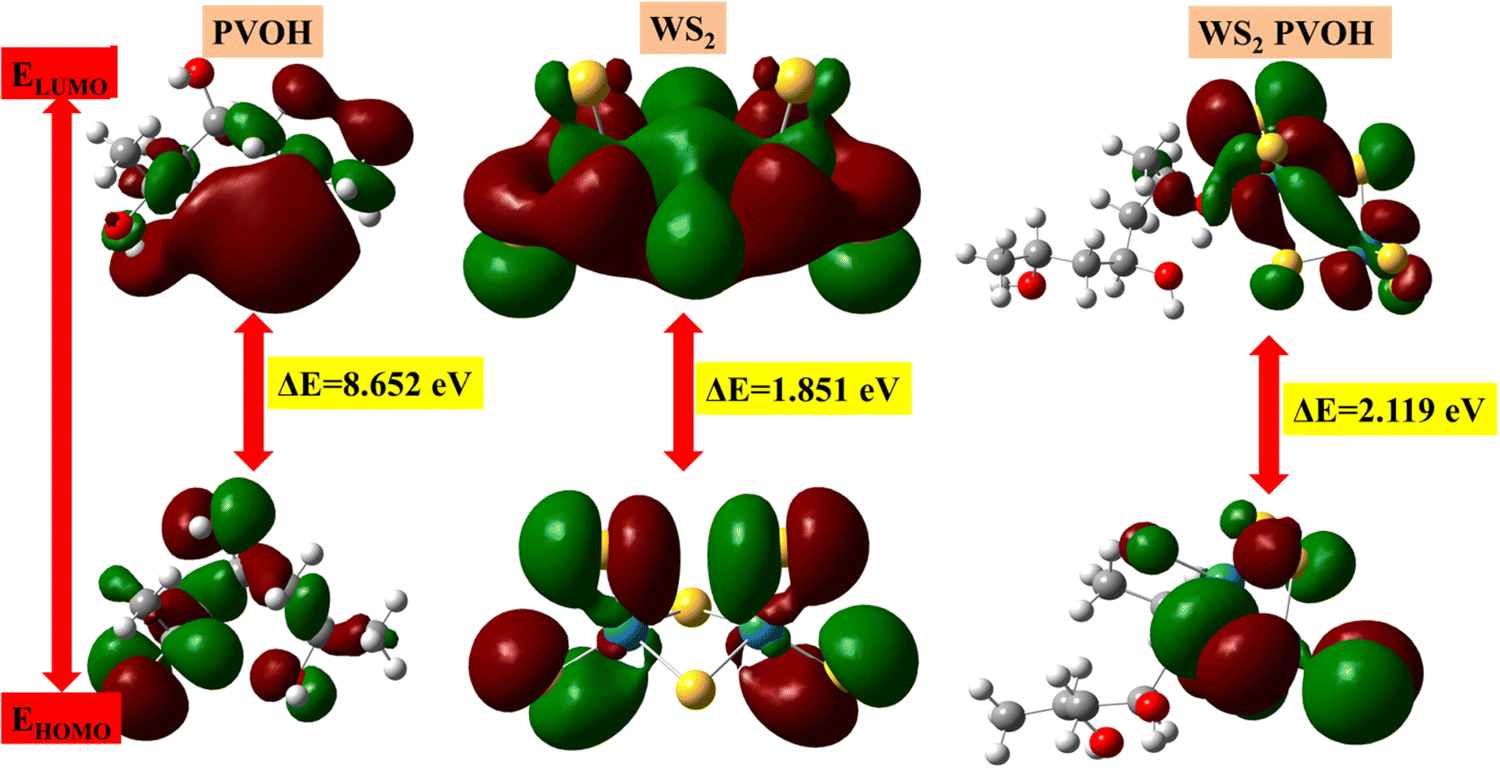
The HOMO is the highest molecular orbital that has any electrons. The second-highest energy orbital is the LUMO orbital (it will be empty). The LUMO is the place where an electron can be positioned or stimulated at the lowest energy. The lowest energy electronic excitation that a molecule is capable of experiencing is typically the energy difference between the HOMO and LUMO. We can learn about the wavelengths that the compound can absorb from this energy gap. In Fig. 12, the HOMO–LUMO gaps represented by red color show the positive phase and green color represents the negative phase. Both positive and negative phases are distributed with all molecules of WS2 and PVOH but in WS2 PVOH it is mostly distributed within WS2 in both the HOMO and LUMO levels, which indicates that most of the electronic charge transfer takes place within WS2 and PVOH provides more stability to the system. The HOMO levels of PVOH, WS2 and WS2 PVOH are found at −7.12, −7.70 and −6.26 eV, whereas the LUMO levels are found at 1.52, −5.94 and −4.14 eV, respectively; on the basis of these results it can be concluded that it is easier to move an electron from the HOMO to LUMO levels because the HOMO level of PVOH and LUMO of WS2 shift to lower levels of −7.12 eV and −5.94 eV. It can also be noted that the HOMO and LUMO levels of WS2 are in between the PVOH HOMO to LUMO levels, which means that electrons travel from WS2 to PVOH for the transition to a higher excited level, which can also be seen in the experimental results of photodetection; for example, two types of transitions are found: one fast rise or decay and a second slow rise or decay. The HOMO–LUMO gap was discovered to be 8.65 eV, 1.85 eV, and 2.11 eV for PVOH, WS2, and WS2 PVOH, according to the examination of the simulation findings. This tells us that when the WS2 nanosheets are added to the PVOH matrix, the excitation energy or absorption energy reduces from pure WS2 sheets and increases as compared to PVOH. Fig. 12 illustrates how the addition of WS2 to the PVOH matrix altered the HOMO–LUMO gap energy. The chemical reactivity parameters based on the values of the HOMO and LUMO energies have been established.70 Understanding the relationship between the HOMO and LUMO energy gaps is essential for defining the chemical reactivity and kinetic stability of polymers as well as understanding static molecular reactivity. The chemical reactivity of the molecule is fundamentally described by its ionization energy. The ionization energy can forecast the reactivity of compounds. A compound's stability is indicated by high ionization energy, whereas its reactivity is shown by low ionization energy.71
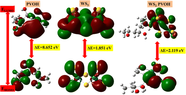 |
| | Fig. 12 HOMO–LUMO based energy gap in (a) PVOH, (b) WS2 and (c) WS2 PVOH. | |
The results of the electron affinity test indicated that the accepted electrons might be bonded to a chemical structure. PVOH typically has an ionization potential of 9 eV. The electron affinity values show that when PVOH, WS2, and WS2 PVOH accept one electron to form a radical anion, they release, respectively, −1.52, 5.94, and 6.26 eV of energy. A lower electron affinity value means that the substance does not readily receive electrons. It follows that WS2 can rapidly accept electrons from the environment in comparison to WS2 PVOH. Absolute hardness and softness, which are inversely correlated, are essential properties. They also gauge a material's molecular stability, reactivity, and electron transfer resistance. The chemical hardness of PVOH, WS2, and WS2 PVOH is determined to be, respectively, 4.32, 0.92, and 1.06 eV. The chemical potential describes the propensity of electrons to escape an equilibrium solution. As the electronic chemical potential rises, the molecule becomes less stable or more reactive.72 The highest chemical potential of −6.86 eV is detected for WS2, whereas it is observed to be −2.79 eV and −5.20 eV for PVOH and WS2 PVOH, respectively. This indicates that the WS2 PVOH system is more stable than the WS2 system. Energy stabilization occurs when a system picks up an extra electronic charge (ΔN) from its surroundings. The tendency of the electrophile to pick up an extra electronic charge driven by us as well as the system's resistance to exchanging electronic charge with the environment described by Nmax are both included in the electrophilicity index. The charge transfer (ΔN) results of 7.42 reveal that WS2 can exchange more electronic charge from the environment but at the same time the lower HOMO–LUMO gap exhibited lower stability, but after conjugating with PVOH, ΔN was found to be 4.91 which shows the higher electronic change exchange capability with higher stability as compared to WS2.
| | | HOMO–LUMO gap (ΔE) = ELUMO − EHOMO | (17) |
| | | Electron affinity (EA) = −ELUMO | (18) |
| | | Ionization potential (IP) = −EHOMO | (19) |
| |  | (20) |
| |  | (21) |
| |  | (22) |
| |  | (23) |
| |  | (24) |
4. Conclusion
It can be concluded from the above discussion that WS2 nanosheets are successfully incorporated into the PVOH matrix, which can be used as a photodetector device. The semi-crystalline character is shown once the WS2 nanosheets have been incorporated into the PVOH matrix. With a band gap of 3.51 eV, the UV-Visible absorbance measurements demonstrate that this material is particularly appropriate for UV light detection. This photodetector device exhibited the highest responsivity of 369.13 mA W−1 with a detectivity of 5.25 × 10¹¹ Jones. As compared to PVOH, WS2-incorporated PVOH shows better performance in terms of photodetector parameters. For the photodetector device based on WS2 PVOH, the photodetector parameters revealed that this device is very useful for UV light detection. On the basis of DFT analysis, it can also be concluded that upon the incorporation of WS2 nanosheets in the PVOH matrix, the HOMO–LUMO gap energy decreased to 2.11 eV as compared to the PVOH energy of 8.65 eV.
Conflicts of interest
There are no conflicts to declare.
Acknowledgements
Mr Arpit Verma and the corresponding author acknowledge the Uttar Pradesh Council of Science and Technology, Lucknow for financial assistance in the form of Project Ref. CST/D-2290. The authors are also thankful to USIC, BBAU, Lucknow for providing characterization facilities such as SEM, XRD, and FTIR.
References
- J. Huang, L. Yan, S. Liu, L. Tao and B. Zhou, Mater. Horiz., 2022, 9, 1167–1195 RSC.
- H. Michaels, I. Benesperi and M. Freitag, Chem. Sci., 2021, 12, 5002–5015 RSC.
- Q. H. Wang, K. Kalantar-Zadeh, A. Kis, J. N. Coleman and M. S. Strano, Nat. Nanotechnol., 2012, 7, 699–712 CrossRef CAS PubMed.
- P. K. Khanna, P. Phalswal, H.-G. Rubahn and Y. K. Mishra, Mater. Adv., 2022, 3, 5672–5697 RSC.
- A. Khunger, N. Kaur, Y. K. Mishra, G. R. Chaudhary and A. Kaushik, Mater. Lett., 2021, 304, 130656 CrossRef CAS.
- W. Zhang, C.-P. Chuu, J.-K. Huang, C.-H. Chen, M.-L. Tsai, Y.-H. Chang, C.-T. Liang, Y.-Z. Chen, Y.-L. Chueh and J.-H. He, Sci. Rep., 2014, 4, 1–8 CrossRef.
- R. K. Tripathi, O. S. Panwar, I. Rawal, C. K. Dixit, A. Verma, P. Chaudhary, A. K. Srivastava and B. C. Yadav, J. Mater. Sci.: Mater. Electron., 2021, 32, 2535–2546 CrossRef CAS.
- A. Verma, P. Chaudhary, A. Singh, R. K. Tripathi and B. C. Yadav, ACS Appl. Nano Mater., 2022, 5, 4860–4874 CrossRef CAS.
- R. Wadhwa, A. V. Agrawal, D. Kushavah, A. Mushtaq, S. K. Pal and M. Kumar, Appl. Surf. Sci., 2021, 569, 150949 CrossRef CAS.
- P. Aggarwal, S. Kaushik, P. Bisht, M. Sharma, A. Singh, B. R. Mehta and R. Singh, Cryst. Growth Des., 2022, 22, 3206–3217 CrossRef CAS.
- J. S. Shaikh, N. S. Shaikh, S. Sabale, N. Parveen, S. P. Patil, Y. K. Mishra, P. Kanjanaboos, S. Praserthdam and C. D. Lokhande, Mater. Today Chem., 2021, 21, 100480 CrossRef CAS.
- N. Dong, Y. Li, Y. Feng, S. Zhang, X. Zhang, C. Chang, J. Fan, L. Zhang and J. Wang, Sci. Rep., 2015, 5, 1–10 Search PubMed.
- R. Wadhwa, A. V. Agrawal and M. Kumar, J. Phys. D: Appl. Phys., 2021, 55, 063002 CrossRef.
- W. Song, Q. Liu, J. Chen, Z. Chen, X. He, Q. Zeng, S. Li, L. He, Z. Chen and X. Fang, Small, 2021, 17, 2100439 CrossRef CAS PubMed.
- L. Britnell, R. V. Gorbachev, R. Jalil, B. D. Belle, F. Schedin, A. Mishchenko, T. Georgiou, M. I. Katsnelson, L. Eaves and S. V. Morozov, Science, 2012, 335, 947–950 CrossRef CAS PubMed.
- A. K. Geim and I. V. Grigorieva, Nature, 2013, 499, 419–425 CrossRef CAS PubMed.
- V. Chaudhary, N. Ashraf, M. Khalid, R. Walvekar, Y. Yang, A. Kaushik and Y. K. Mishra, Adv. Funct. Mater., 2022, 32, 2112913 CrossRef CAS.
- V. Chaudhary, A. K. Kaushik, H. Furukawa and A. Khosla, ECS Sensors Plus, 2022, 1, 013601 CrossRef.
- L. Shooshtari, S. Ghods, R. Mohammadpour and A. Esfandiar, Sci. Rep., 2022, 12, 1–14 CrossRef PubMed.
- W. Zhu, T. Low, H. Wang, P. Ye and X. Duan, 2D Mater., 2019, 6, 032004 CrossRef CAS.
- A. Singh, S. Sikarwar, A. Verma and B. C. Yadav, Sens. Actuators, A, 2021, 332, 113127 CrossRef CAS.
- D. Jariwala, T. J. Marks and M. C. Hersam, Nat. Mater., 2017, 16, 170–181 CrossRef CAS PubMed.
- P. Chaudhary, A. Verma, A. Mishra, D. Yadav, K. Pal, B. C. Yadav, E. R. Kumar, K. B. Thapa, S. Mishra and D. K. Dwivedi, Phys. E, 2022, 139, 115174 CrossRef CAS.
- A. Verma, U. Kumar, P. Chaudhary and B. C. Yadav, Solid State Commun., 2022, 348, 114723 CrossRef.
- S. Cai, X. Xu, W. Yang, J. Chen and X. Fang, Adv. Mater., 2019, 31, 1808138 CrossRef PubMed.
- A. Singh, A. Verma, B. C. Yadav and P. Chauhan, Dalton Trans., 2022, 51, 7864–7877 RSC.
- D. Zhu, D. Ji, L. Li and W. Hu, J. Mater. Chem. C, 2022, 10, 13312–13323 RSC.
- L. Shi, Q. Liang, W. Wang, Y. Zhang, G. Li, T. Ji, Y. Hao and Y. Cui, Nanomaterials, 2018, 8, 713 CrossRef PubMed.
- Z. Zhong, K. Li, J. Zhang, L. Ying, R. Xie, G. Yu, F. Huang and Y. Cao, ACS Appl. Mater. Interfaces, 2019, 11, 14208–14214 CrossRef CAS PubMed.
- M. Ahmadi, T. Wu and B. Hu, Adv. Mater., 2017, 29, 1605242 CrossRef PubMed.
- J. Yang, J.-U. Lee and H. Cheong, FlatChem, 2017, 3, 64–70 CrossRef CAS.
- W. Zhao, Z. Ghorannevis, K. K. Amara, J. R. Pang, M. Toh, X. Zhang, C. Kloc, P. H. Tan and G. Eda, Nanoscale, 2013, 5, 9677–9683 RSC.
- K.-G. Zhou, F. Withers, Y. Cao, S. Hu, G. Yu and C. Casiraghi, ACS Nano, 2014, 8, 9914–9924 CrossRef CAS PubMed.
- A. Berkdemir, H. R. Gutiérrez, A. R. Botello-Méndez, N. Perea-López, A. L. Elías, C.-I. Chia, B. Wang, V. H. Crespi, F. López-Urías and J.-C. Charlier, Sci. Rep., 2013, 3, 1–8 Search PubMed.
- S. B. Aziz, I. Brevik, M. A. Brza, A. S. F. M. Asnawi, E. Dannoun, Y. M. Yusof, R. T. Abdulwahid, M. H. Hamsan, M. M. Nofal and M. F. Z. Kadir, Materials, 2020, 13, 5030 CrossRef CAS PubMed.
- R. Ricciardi, F. Auriemma, C. De Rosa and F. Lauprêtre, Macromolecules, 2004, 37, 1921–1927 CrossRef CAS.
- S. Sikarwar, B. C. Yadav, S. Singh, G. I. Dzhardimalieva, S. I. Pomogailo, N. D. Golubeva and A. D. Pomogailo, Sens. Actuators, B, 2016, 232, 283–291 CrossRef CAS.
- P. Chaudhary, D. K. Maurya, A. Pandey, A. Verma, R. K. Tripathi, S. Kumar and B. C. Yadav, Sens. Actuators, B, 2022, 350, 130818 CrossRef CAS.
- P. Rademeyer, D. Carugo, J. Y. Lee and E. Stride, Lab Chip, 2015, 15, 417–428 RSC.
- B. Lorber, F. Fischer, M. Bailly, H. Roy, D. J. B. Kern and M. B. Education, Biochem. Mol. Biol. Educ., 2012, 40, 372–382 CrossRef CAS PubMed.
- A. Verma, D. Yadav, A. Singh, M. Gupta, K. B. Thapa and B. C. Yadav, Sens. Actuators, B, 2022, 361, 131708 CrossRef CAS.
- S. Bhattacharjee, J. Controlled Release, 2016, 235, 337–351 CrossRef CAS PubMed.
- V. R. Patel and Y. K. Agrawal, J. Adv. Pharm. Technol. Res., 2011, 2, 81 CrossRef CAS PubMed.
- A. Singh, P. Chauhan, A. Verma and B. Chandra Yadav, Sustainable Energy Fuels, 2023, 7, 131–143 RSC.
- S. F. Alvarado, P. F. Seidler, D. G. Lidzey and D. D. C. Bradley, Phys. Rev. Lett., 1998, 81, 1082 CrossRef CAS.
- L. Li, F. Zhang, J. Wang, Q. An, Q. Sun, W. Wang, J. Zhang and F. Teng, Sci. Rep., 2015, 5, 1–7 Search PubMed.
- A. Verma, P. Chaudhary, R. K. Tripathi and B. C. Yadav, Mater. Adv., 2022, 3, 3994–4005 RSC.
- Z. Zhang and J. T. Yates Jr, Chem. Rev., 2012, 112, 5520–5551 CrossRef CAS PubMed.
- B. D. Boruah, Nanoscale Adv., 2019, 1, 2059–2085 RSC.
- R. Raj, P. Lohia, D. Dwivedi, A. Verma and B. C. Yadav, J. Mater. Sci.: Mater. Electron., 2022, 1–10 Search PubMed.
- B. Philippa, R. White and A. Pivrikas, Appl. Phys. Lett., 2016, 109, 153301 CrossRef.
- A. Verma, P. Chaudhary, R. K. Tripathi and B. C. Yadav, Sens. Actuators, A, 2021, 321, 112600 CrossRef CAS.
- A. Verma, P. Chaudhary, R. K. Tripathi, A. Singh and B. C. Yadav, J. Inorg. Organomet. Polym. Mater., 2022, 32, 2807–2826 CrossRef CAS.
- M. Zhu, Z. Zhao, Y. Fang, C. Fang, Z. Weng, W. Lei, S. B. Shafie and M. N. Mohtar, Appl. Phys. A: Mater. Sci. Process., 2021, 127, 1–8 CrossRef.
- C. Gautam, A. Verma, P. Chaudhary and B. C. Yadav, Opt. Mater., 2022, 123, 111860 CrossRef CAS.
- D. Kannichankandy, P. M. Pataniya, C. K. Zankat, M. Tannarana, V. M. Pathak, G. K. Solanki and K. D. Patel, Appl. Surf. Sci., 2020, 524, 146589 CrossRef CAS.
- D. Nath, P. Dey, A. M. Joseph, J. K. Rakshit and J. N. Roy, Opt. Mater., 2020, 108, 110371 CrossRef CAS.
- A. Verma, P. Chaudhary, R. K. Tripathi and B. C. Yadav, Sustainable Energy Fuels, 2021, 5, 1394–1405 RSC.
- K. Arora, K. Kaur and M. Kumar, ACS Appl. Electron. Mater., 2021, 3, 1852–1863 CrossRef CAS.
- D. Nath, P. Dey, A. M. Joseph, J. K. Rakshit and J. N. Roy, Opt. Laser Technol., 2020, 131, 106393 CrossRef CAS.
- A. A. Hussain, ACS Appl. Mater. Interfaces, 2020, 12, 46317–46329 CrossRef CAS PubMed.
- S.-W. Lee, K.-J. Choi, B.-H. Kang, J.-S. Lee, S.-W. Kim, J.-B. Kwon, S.-A. Gopalan, J.-H. Bae, E.-S. Kim and D.-H. Kwon, Org. Electron., 2016, 39, 250–257 CrossRef CAS.
- R. A. Talib, M. Abdullah, H. S. Al-Salman, S. M. Mohammad and N. K. Allam, Mater. Chem. Phys., 2016, 181, 7–11 CrossRef CAS.
-
A. Frisch, Gaussian 09, Wallingford, USA, 2009, vol. 470 Search PubMed.
-
G. J. Zheng, L. Sonnenberg, M. Hada, M. Ehara, K. Toyota, R. Fukuda, J. Hasegawa, M. Ishida, T. Nakajima and Y. Honda, Gaussian 09, Gaussian Inc., Wallingford CT, 2009 Search PubMed.
- N. Xu, J. Chen, Q. Wei, E. Ding, X. Zeng, F. Xue, N. Zhang and J. Shang, J. Appl. Polym. Sci., 2020, 137, 48487 CrossRef CAS.
- U. Kumar, H.-W. Hsieh, Y.-C. Liu, Z.-Y. Deng, K.-L. Chen, W.-M. Huang and C.-H. Wu, ACS Appl. Mater. Interfaces, 2022, 14(28), 32279–32288 CrossRef CAS PubMed.
- U. Kumar, Y.-H. Yang, Z.-Y. Deng, M.-W. Lee, W.-M. Huang and C.-H. Wu, Sens. Actuators, B, 2022, 353, 131192 CrossRef CAS.
- S. Singh, P. Yadav, M. K. Gupta, G. I. Dzhardimalieva, J. Yoon, C. Maiti and B. C. Yadav, Sens. Actuators, B, 2022, 359, 131573 CrossRef CAS.
- S. Sikarwar, A. Pandey, A. Singh, B. C. Yadav, I. E. Uflyand and G. I. Dzhardimalieva, Mater. Sci. Eng., B, 2022, 283, 115813 CrossRef CAS.
- G. Maheswari and R. V. Williams, Int. J. Res. Anal. Rev., 2019, 6, 513–528 Search PubMed.
- R. Molavi, R. Safaiee and M. H. Sheikhi, Phys. Chem. Chem. Phys., 2020, 22, 14889–14899 RSC.
|
| This journal is © The Royal Society of Chemistry 2023 |
Click here to see how this site uses Cookies. View our privacy policy here. 
 Open Access Article
 This Open Access Article is licensed under a Creative Commons Attribution-Non Commercial 3.0 Unported Licence
 a,
Anshika
Singh
a,
Anshika
Singh