
 Open Access Article
 This Open Access Article is licensed under a Creative Commons Attribution-Non Commercial 3.0 Unported Licence
Rational and key strategies toward enhancing the performance of graphene/silicon solar cells
Parisa
Fallahazad

Materials and Energy Research Center, Department of semiconductor, Karaj, Iran. E-mail: p.fallahazad@merc.ac.ir
First published on 12th April 2023
Abstract
Graphene has attracted considerable attention due to its unique physical and chemical properties. Thanks to its atomic thickness, high carrier mobility, and transparency, graphene is the best electrode material for a wide range of optoelectronic devices such as solar cells, light-emitting diodes, and photodetectors. Improvement of graphene/silicon (Gr/Si) solar cells has gained significant research interest in the field of semiconductor devices. Herein, a comprehensive review of Gr/Si solar cells is provided with a detailed introduction of the structure, mechanism, and fundamental physics of Gr/Si solar cells. Then, various key strategies to improve the performance of the solar cells are summarized. The article concludes with the goals and direction for future works on graphene-based solar cells.
 Parisa Fallahazad | She is a semiconductor science researcher, materials specialist, and solid state physicist. She received her MSc in thin film physics from the Materials and Energy Research Center (MERC). Her research interests include surface texturing, solar cells, and optoelectronic devices. |
1. Introduction
The modern world is completely tied to energy consumption due to the drastic changes in our lifestyles over the past few decades. However, the limitation of traditional energy resources is one of the most significant problems, posing a serious crisis. Various sources of energy, including fossil fuels, thermal, nuclear, hydroelectric, wind, natural gas, and sun have been employed to fulfill our growing demand for energy in almost all aspects of our daily life. To meet global energy demand, novel technologies should be explored for effective, clean, and affordable methods of energy generation, storage, and use. Such a rising energy demand has led to the development of renewable methods of energy generation, storage, and use. Solar cells have drawn tremendous interest among some renewable energy sources such as tidal and wind energy as they can meet the ever-increasing demand for clean energy. The energy of the sun is the most inexpensive, safest, and cleanest renewable energy source in the world.1,2Conventional silicon solar cells based on p–n junctions have high efficiency and long-term stability,3 however, they have a high fabricating cost due to the need for high-quality silicon,and the complicated manufacturing steps restrict their widespread usage.4,5 New materials, technologies, and fabrication processes have, therefore, been explored. Solar cells with heterojunction structures, including carbon materials, have attracted much attention nowadays because carbon is a rich element in nature and can be made at low cost with economies of scale in production.6 Investigations of carbon materials have been carried out due to their structural variety and unique texture, features, and applications. Since the 1960s, new carbon materials that differ from traditional carbon materials (such as carbon black, activated carbon, and graphite) have been produced. Carbon nanomaterials, in the form of stable allotropes (such as carbon nanotubes, graphene, fullerene, nanofibers, etc.), are significant building blocks of nanotechnology.7 Notably, one-dimensional (1D) carbon nanotubes (CNTs) and two-dimensional (2D) graphene members of the family of carbon nanomaterials exhibit outstanding electronic and optoelectronic properties that make them excellent alternatives for energy conversion.8,9
Carbon nanotubes are hollow cylinders constructed by rolling up a graphene sheet, which is a vast planar hexagonal lattice of only sp2-bonded carbons first reported in 1991.10 Moreover, carbon nanotube has several benefits, including high charge carrier mobility, ballistic transport properties, high optical transmittance, and low light reflectance, which satisfies the prerequisite of heterojunction-based solar cells very well.11,12 However, there are challenges in setting up adequate contacts between CNTs and semiconducting materials, such as silicon, to create a working heterojunction.13 Graphene is another carbon nanomaterial, which has superior electrical, optical, and mechanical properties, high carrier mobility, as well as low absorbance,14–16 and can be manufactured and handled into ultrathin films,17,18 sheets,19–21 ribbons,22,23 fibers,24,25 and large-surface papers.26
Hence, the applications of this graphene have been widely investigated in different fields, from spectroscopy to nanoelectronic devices, photonics,27 solar cells,28–30 transistors,31 fuel cells,32,33 supercapacitors,34,35 photocatalysts,36 sensors,37 mass spectrometry,38 and drug delivery.39 In addition, with the introduction of graphene in 2004, many 2D materials were successfully manufactured using different methods, such as chemical and physical vapor deposition methods.40,41 Li et al. first demonstrated the synthesis of Gr by chemical vapor deposition, which is the standard and common technique to produce large-area and high-quality graphene sheets.42–44 In general, Graphene is an attractive material for optoelectronic devices due to its several merits over other materials.45–48
The flexibility of graphene can help to alter the crystal structure or size of carbon at the nano-scale and can greatly assist the investigators to adjust the electrical and optical features of carbon nanomaterial. Research has shown that carbon/silicon solar cells, which are formed by constructing a transparent carbon layer, especially in Si semiconductor silicon-based solar cells, indicate a good potential or prospect for the future of solar cells.47,48
2. An overview of the characteristics of graphene
Graphite oxide and graphene oxide (GO), an oxidized single- or multi-layered unique graphene sheet, are forerunners to graphene (Fig. 1). Both of these structures contain hydroxyl (–OH) and epoxide (–C–O–C–) functional groups on their basal planes, and carbonyl (–COH) and carboxyl (–COOH) functional groups at their edges. Gao et al. introduced the presence of 5-and 6-membered-ring lactols in a graphite oxide or GO structure. GO is suitable for coordination with other molecules and materials due to its surface functional groups such as hydroxy, carboxyl, and epoxy groups. Due to the wide variety of structures, GO and its composites can be employed for energy storage and environmental protection applications, such as water purification and air pollutant removal.49–51 GO also bears oxygen functional groups which can be partially eliminated by a variety of reduction processes such as high-temperature thermal annealing52 and chemical reduction with hydrazine.53 The elimination of oxygen groups from the GO promotes its thermal stability and electrical conductivity. The thermal reduction of GO to graphene involves the removal of carboxyl, hydroxyl, and epoxy groups. Mathkar et al. systematically investigated GO reduction to adjust its bandgap.55 They found that the optical bandgap of GO changed from 3.5 eV to 1.0 eV due to the controlled reduction process. Structural modification from GO to rGO and then to graphene is accompanied by slow changes in the optical band gap, electrical conductivity, charge carrier mobility, and thermal stability. These properties have a remarkable effect on the photovoltaic characteristics and stability of graphene-based solar cells. Therefore, rGO has been broadly investigated in solar cell applications.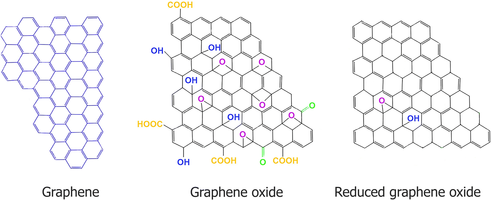 | ||
| Fig. 1 Chemical structure of graphene, graphene oxide (GO), and reduced graphene oxide (rGO). Reproduced from ref. 54, with permission from the Royal Society of Chemistry. | ||
3. A brief overview of graphene/silicon solar cell
3.1 Graphene in silicon solar cell
Graphene is a single layer of carbon atoms arranged in a hexagonal structure with numerous remarkable properties.56 The transparency of the Gr layer in the near-infrared and visible light range can reach 98%.57,58 In addition to flexibility, graphene is also abundant worldwide. This structure is generally popular in large-scale synthesis due to its high mechanical strength, stability, and crystal quality compared to other 2D materials such as MoS2 and hexagonal boron nitride (hBN).59,60 In general, the graphene bandgap can be adjusted from a semiconductor to a semi-metal, depending on its intrinsic physical and electronic features. On the other hand, graphene can replace such as indium tin oxide (ITO) and fluorine tin oxide (FTO) to fabricate transparent electrodes for low-cost solar cells as the restricted resources of indium lead to high manufacturing costs.61,62 Moreover, the vulnerability and fragility of ITO limit its application in flexible devices. Apart from the above-mentioned benefits, graphene outperforms new two-dimensional materials (such as dichalcogenides and black phosphorus) in optoelectronics and semiconductor devices.3.2 Operation principles and band structure of graphene/silicon solar cells
The structure of graphene/silicon (Gr/Si) solar cells and charge-carrier transport across the surface junction are shown in Fig. 2(a) and (b). A built-in electric field is formed at the interface of graphene and silicon upon their contact due to the differences in their work functions. Such a built-in potential at the interface of rGO/Si assists to separate the photogenerated electrons and holes, which can be converted into electrical power. This section will address the current–voltage (I–V) characteristics and basic parameters of photovoltaic cells. Solar cells work based on the principle of the junction effect in semiconductor materials. The solar cell function, i.e., the ability to generate electricity from sunlight, can be estimated based on 4 parameters; short circuit current (Jsc), solar cell open circuit voltage (Voc), and fill factor (FF), which eventually define the power conversion efficiency (PCE).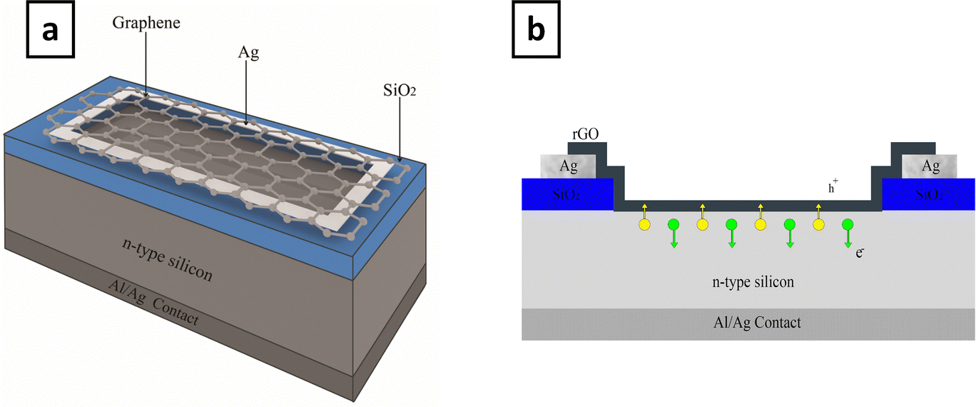 | ||
| Fig. 2 (a) Schematic of a graphene-on-semiconductor (Si) solar cell. (b) Electron–hole pairs transport across the surface junction. Reproduced from ref. 159, with permission from Elsevier. | ||
The mentioned parameters are the major criteria in the assessment of solar cell operation. All of them can be determined from the Current density–voltage curves of the devices exposed to solar simulator radiation under AM 1.5 conditions. When graphene/Si solar cells are open-circuited, the separation of photoelectric carriers generates Voc. When a solar cell is short-circuited, the separated photovoltaic carriers can pass over the external circuit, creating an Isc.
The current density (J) and open circuit voltage (Voc) of a silicon solar cell can be calculated by the following equations:63
| J = Jsc − Js[exp(eV/ηkB − 1)] | (1) |
| Voc = (ηkBT/e)ln[Jsc/Js + 1] | (2) |
The fill factor (FF) of a solar cell can be determined based on the ratio of maximum current density, Jmax, and voltage, Vmax to the product of Jsc and Voc.
The PCE of a solar cell is determined as the incident power converted into electricity which can be expressed by:64
| FF = (JmaxVmax/JscVoc) | (3) |
| PCE = (JscVocFF/Plight) × 100% | (4) |
For the sake of brevity, this short review avoids detailed descriptions of basic concepts which are illustrated in books on the topic of Gr/Si solar cells. In this sub-section, we examine the trend and enhancement of the main parameter in Gr/Si solar cells that were reported by some experimental results also can be categorized into three sectors:
1. Open circuit voltage improvement, which is associated with the height of the Schottky barrier.
2. Short circuit current density improvement, which is associated with the light absorption by silicon surface substrate.
3. Fill factor improvement, corresponds to the reduction of the minority carrier recombination.
This review concentrates only on the application of graphene in the structure of solar cell devices. Moreover, the band structure of graphene-based solar cells and alternative robust solutions for enhancing the performance of this kind of solar cell will be addressed. The limitations will be also discussed in the next sections.
4. Various strategies for optimization of graphene/silicon solar cells
Poor solar cell performance can be due to the following reasons: (1) the single-layer graphene has a low work function (4.4 eV) and large sheet resistance (several kΩ).65 The low work function can reduce the barrier height, which will decline the built-in electric field and obdurate electron–hole pairs separating.66On the other hand, the series resistance may be high for high sheet resistance. (2) The flat silicon wafer absorbs a limited number of photons (30–40% of visible light, 350–800 nm).67 Since the introduction of graphene/Si solar in 2010,68 various methods have been developed to adjust its work function, improve the conductivity of graphene, and reduce the reflectance of silicon wafers. These methods include chemical doping,69–74 increasing the number of the layers of graphene,75,76 and presenting an interlayer,77–82 controlling of the reflectivity with antireflection layer83 and using III–V semiconductors,84 all of which can optimize the efficiency of solar cells significantly.
4.1 Interface engineering
The power conversion efficiency (PCE) of graphene/Si solar cells can be improved through different strategies. This parameter can mainly be limited by the intense recombination of charge carriers at the interface because of the low barrier height. One strategy is to embed a dielectric passivation layer between graphene and the silicon substrate. This extra insulating layer can suppress the diffusion of electrons from the n-Si substrate into the graphene layer, hence, reducing carrier recombination and facilitating the transfer of holes to the graphene layer during the tunneling process. This phenomenon can enhance the Voc and PCE of solar cells.The most suitable insulating layer materials for this purpose are silicon dioxide (SiO2),85,86 molybdenum disulfide (MoS2),87 aluminum oxide (Al2O3),88 graphene oxide (GO),89 hexagonal boron nitride (h-BN),90 poly(3-hexyl thiophene-2,5-diyl) (P3HT),91,92 quantum dots,93,94 Molybdenum trioxide (MoO3),95 and spiroOMeTAD.96
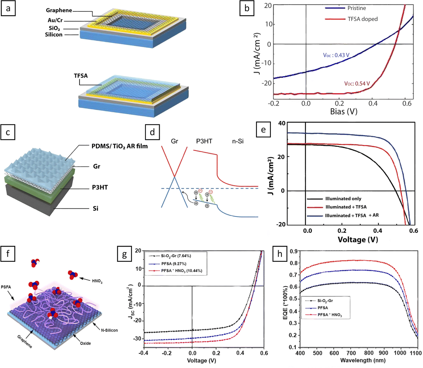
Song et al.97 used an optimal thickness of the SiO2 layer as a layered electron-blocking layered to improve the performance of the solar cell (Fig. 3(a)). Their outcomes indicated an increment in the efficiency of the device from 7.9% to 12.4% upon increasing the thickness of oxide from 5 to 15 Å (Fig. 3(b)). TiO2 anti-reflective coating (ARC) and chemical doping (AuCl3) were also employed in the solar cells with efficiencies as high as 15.6% (Fig. 3(c)).
 | ||
| Fig. 3 (a) Schematic representation of graphene/n-silicon solar cell. (b) J–V properties of graphene/n-silicon solar cell for various oxide thicknesses. (c) Comparison of two solar cells with and without oxide layer and anti-reflective coating (ARC). Reproduced from ref. 97, with permission from the American Chemical Society. (d) Schematic diagram of graphene/h-BN/Si device. (e) The band diagram of the graphene/Si solar cells with and without an h-BN layer. (f) J–V of the device with and without an interlayer. Reproduced from ref. 99, with permission from Elsevier. | ||
In another report, Jiao et al. and Yang et al.98 employed graphene oxide as an interfacial layer to improve the efficiency of the solar cell. They altered the annealing temperatures to achieve higher PCE values. By employing the GO film, the PCE declined from 2.13% to 0.2%, but after increasing the annealing temperature up to 400 °C, the efficiency showed an improvement of up to 5.2%. To reduce the surface recombination in the graphene/n-silicon solar cell, Meng et al.99 used a few-layer boron nitride (h-BN) which was sandwiched between graphene and n-silicon. It also offers the advantage of a hole transport layer. The few-layer graphene was synthesized on Cu foils by a low-pressure CVD method. As shown in Fig. 3(d), several layers of hBN and graphene were deposited onto a silicon substrate by the layer-by-layer (LBL) transfer process and the CVD method, respectively. Moreover, the band structure of the graphene/n-silicon solar cell is shown in Fig. 3(e) after modification. After depositing the hBN layer, photovoltaic properties such as Vocs and PCEs raised from 0.412 to 0.474 V and from 3.75% to 4.40% in the original cells, respectively (Fig. 3(f)). The graphene/h-BN/Si solar cell exhibited an initial PCE of 4.40%, which improved to 10.93% by co-doping of graphene with Au nanoparticles and HNO3. In contrast to SiO2 and Fluorograph, the hBN layer shows no trapped charge or surface states. Hexagonal Boron Nitride (hBN) is an sp2-hybridized 2D insulator with a very smooth surface having no dangling bonds. In addition, hBN is isoelectronic with a structure similar to graphene. Its low lattice mismatch (only 1.7%) allows compatible graphene/hBN heterostructures with suppressed interface recombination and elevated open-circuit voltage.100–103
Zhang et al.104 fabricated graphene nanowalls (GNWs)/Si solar cells and improved the device with an interface engineering solution. They also used a polymer-free transfer method (PFTM) of GNWs grown on the copper foil to manufacture the device. They fabricated three types of GNWs/Si solar cells to compare the effect of the spiro-OMeTAD interface layer. Fig. 4(a) demonstrates the diagram of three as-prepared solar cells, where A, B, and C illustrate spiro-OMeTAD/n-Si, GNWs/n-Si, and GNWs/spiro-OMeTAD/n-Si solar cells, respectively. It should be noted that spiroOMeTAD is a highly profitable p-type organic semiconductor with extensive applications as a hole-transport layer in organic devices (Fig. 4(b)). The Optimization of the thickness of the spiro-OMeTAD layer is also a significant parameter influencing the solar cell performance. Various thicknesses of the spiro-OMeTAD thin film were formed through diverse concentrations of the spin-coating solution (10–70 mg ml−1). The highest PCE (8.27%) was recorded in the case of the GNWs/spiro-OMeTAD/Si device, at the spiro-OMeTAD concentration of 30 mg ml−1 with an estimated layer thickness of ∼33 nm. Further increase in the concentration of the spiro-OMeTAD solution, however, led to the opposite effect (Fig. 4(c)). The effect of Molybdenum trioxide (MoO3) was investigated on the photovoltaic characteristics of graphene/Si solar cells by S. Chandramohan, et al.105 (Fig. 4(d)). MoO3 is one of the best transition metal oxides which can improve the work function of graphene. By employing the MoO3 onto graphene, the PCE was improved from 0.86% to 3.5% (Fig. 4(e)). A maximum efficiency of 4% was obtained for the MoO3/Ag/MoO3 multilayer (MAM) solar cell. The MoO3/Ag/MoO3/graphene structure showed a sheet resistance of 10 Ω sq−1, which is 98% and 97% lower than that of pristine graphene and MoO3-coated graphene, respectively.
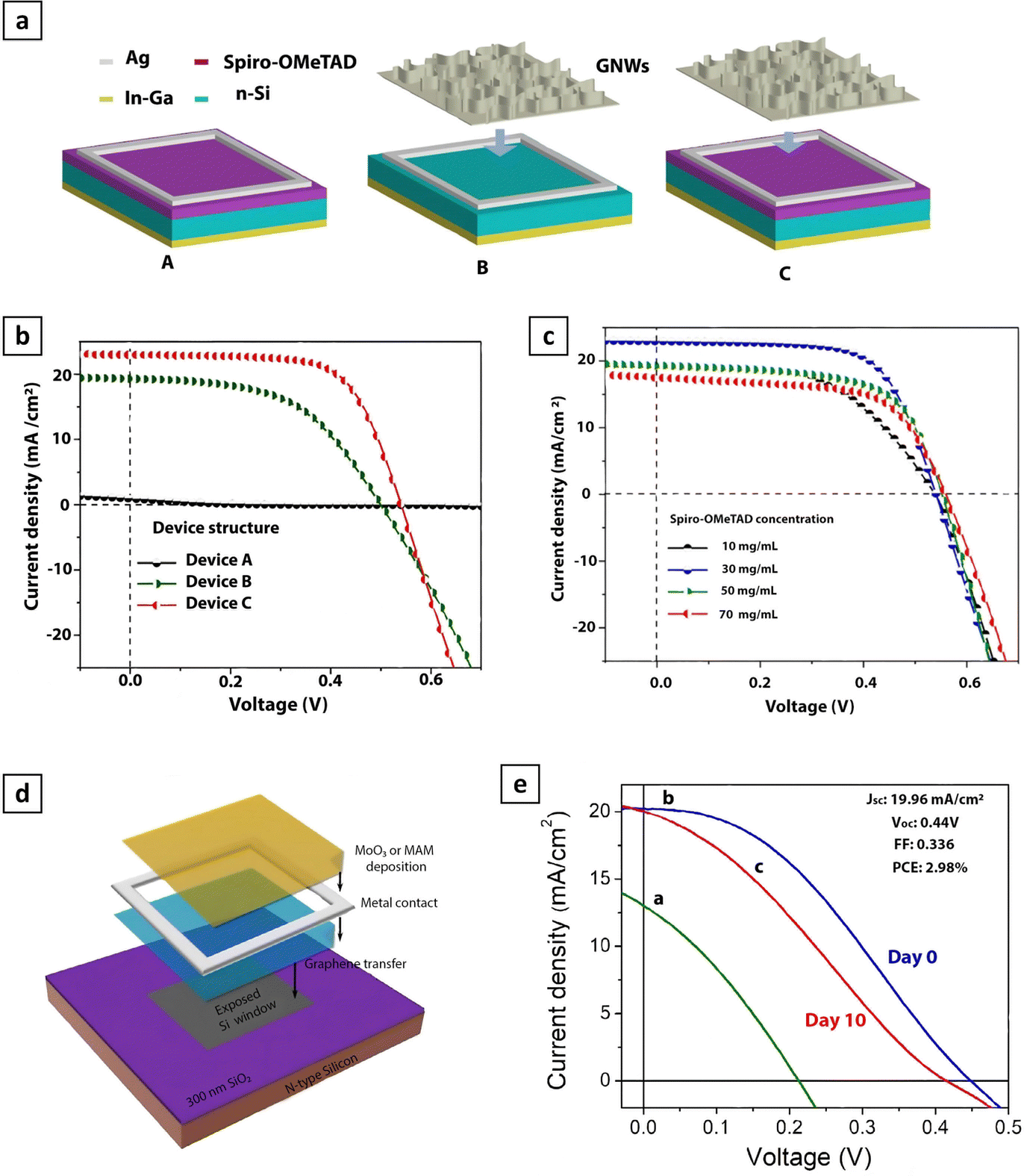 | ||
| Fig. 4 (a) Schematic structure of three sets of the devices: spiro-OMeTAD/n-Si solar cell; GNWs/n-Si solar cell; GNWs/spiro-OMeTAD/n-Si solar cell. (b) J–V characteristics of the three sets of structured GNWs/Si solar cells. (c) J–V characteristics of the device with different concentrations of the spiro-OMeTAD. Reproduced from ref. 104, with permission from American Institute of Physics. (d) Schematic diagram demonstrating the steps of device construction. (e) J–V characteristics of the devices manufactured with and without MoO3 film. Reproduced from ref. 105, with permission from Elsevier. | ||
In 2017, Alnuaimi et al.106 reported the improved performance of Gr/Si Schottky barrier solar cells (SBSC) by engineering the interface with the aluminum oxide (Al2O3) layer. The device structure and band diagram are shown in Fig. 5(a)–(c). The advantage of the Al2O3 interface layer is not just restricted to forming a higher Schottky barrier as it also decreases the recombination at the interface. In Schottky barrier solar cells (SBSC), the tunneling of holes should dominate over the recombination to gain effective charge carrier transport. Based on Song et al.107 the presence of a layer of native oxide at the interface between the graphene and silicon permits the tunneling of holes. But the native oxide thickness grows continually, declining the operation of Gr/Si solar cells over time. As displayed in Fig. 5(b), by increasing the native oxide thickness, the tunneling of holes decreases. This phenomenon leads to accumulation at the interface, increasing the charge carrier recombination. Therefore, the use of the SiO2 intermediate layer poses a major problem affecting the performance stability of Gr/Si SBSC. As indicated in Fig. 5(c), deposition of the Al2O3 layer on the native oxide surface controls the creation of thick native oxide at the interface. The formation of the Al2O3 layer also helps in decreasing surface recombination, enhancing the carrier lifetime for the silicon surface, and declining the series resistance. Thus, the enhancement in solar cell efficiency with the Al2O3 interfacial layer can be assigned to the passivation of the silicon surface, which diminishes surface recombination, leading to higher SBH, which facilitates the transport of charge carriers. Al2O3-containing solar cells indicated an enhancement in PCE from 7.2% to 8.7% and acceptable stability after 28 days of operation (Fig. 5(d) and (e)).
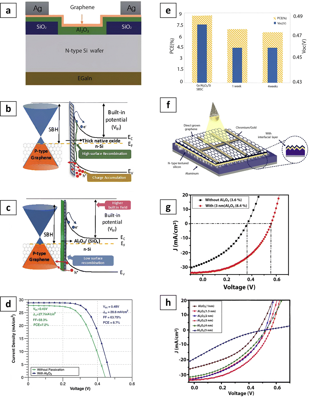 | ||
| Fig. 5 (a) Schematic of Gr/Al2O3/Si device. (b) and (c) the energy band diagram of devices with and without Al2O3 layer. (d) J–V characteristics of devices. (e) Variations of PCE and Voc of Gr/Si with Al2O3 interfacial layer by time. Reproduced from ref. 106, with permission from the Royal Society of Chemistry. (f) Metal–insulator–semiconductor Schottky solar cells by Al2O3 layer. (g) J–V characteristics of the devices under illumination with and without an Al2O3 layer. (h) Comparison of J–V for different thicknesses of the Al2O3 layer. Reproduced from ref. 108, with permission from Elsevier. | ||
In another study, Rehman et al.108 manufactured a high-efficiency n-type textured Si/Al2O3 solar cell by instant transfer of graphene on the substrate using plasma enhanced chemical vapor deposition (PECVD) (Fig. 5(f)). They transfer a small number of layers of graphene on top of Al2O3/Si through plasma-enhanced chemical vapor deposition. Finally, by optimizing the thickness of the Al2O3 layer interlayer (30 Å), the maximum efficiency of 8.4% was obtained without passivation thin film or intentional doping due to decreased surface recombination at the interface (Fig. 5(g) and (h)).
MoS2 layers in graphene solar cells have attracted great attention in recent years due to their unique band structure, high absorption coefficient, and electrical properties. The MoS2 interlayer can operate as a hole transport layer to simplify the separation of electron–hole pairs. Moreover, it acts as an electron blocking layer to quench the recombination at the interface. Ma et al.109 prepared a high-efficiency graphene/MoS2/Si solar cell (Fig. 6(a)) in which the graphene and MoS2 monolayers were deposited by a spin-coated method. The MoS2 interlayers could dramatically enhance the efficiency of the device and the thickness of the layer could be controlled via direct sulfurization of pre-annealed molybdenum foil. By optimizing the thickness of MoS2 layers (4 nm), a high efficiency (13.1%) was achieved for graphene/MoS2/Si Schottky barrier solar cells (Fig. 6(b)). Likewise, TiO2 anti-reflective coating (ARC) was also used which incremented the efficiency to 15.8% (Fig. 6(c)).
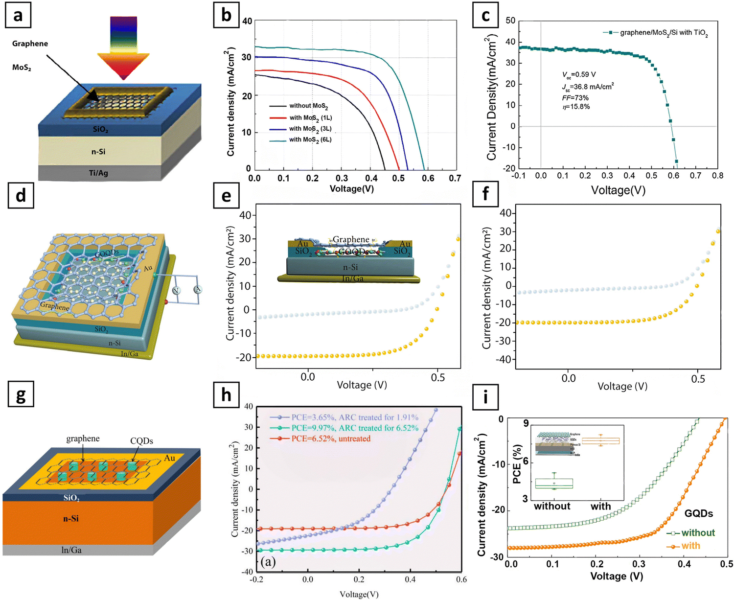 | ||
| Fig. 6 (a) A schematic representation of graphene/MoS2/Si Schottky barrier solar cells. (b) J–V characteristic of graphene/MoS2/Si Schottky solar cells. (c) J–V characteristics of the device with antireflective layer. Reproduced from ref. 109, with permission from Elsevier. (d) Schematic design of metal–insulator–semiconductor with GOQD interlayer barrier. (e and f) J–V characteristic curve for the optimal GOQD size and thickness. Reproduced from ref. 110, with permission from Science Partner Journals. (g) Schematic structure of the Gr/CQDs/Si solar cells. (h) J–V characteristics of the Gr/CQDs/Si solar cells. Reproduced from ref. 111, with permission from Science Partner Journals. (i) J–V characteristic of the solar cells with/without GQDs. Reproduced from ref. 112, with permission from Elsevier. | ||
The effect of the graphene oxide quantum dots (GOQDs), as a high-quality interfacial, were explored layer on the graphene/n-Si solar cells by Geng et al.110 GOQDs can adjust the interface properties of Gr/Si Schottky barrier solar cells (SBSCs) and act as a distinctive barrier at the interface (Fig. 6(d)). The association between PCE and the particle size and thickness of GOQDs was also evaluated. The hole tunneling and the carrier recombination rate can be handled by the thickness and particle size of the GOQDs barrier in the Gr/Si SBSCs. The GOQD-induced additional band flexure in Gr/Si-based SBSCs supplies a process for enhanced PCE. The best efficiency (with Jsc, Voc, FF, and PCE of 19.01 mA cm−2, 0.47 V, 74.07, and 6.75) was recorded at the GOQDs size of 4.15 (Fig. 6(e)). The optimal GOQD thickness was 26 nm as Jsat of the solar cell drops from 2.19 × 10⁻⁸ A cm−2 to 8.14 × 10⁻⁹ A cm−2, suggesting that the carrier recombination is virtually stifled. According to their result, the best PCE of Gr/Si-based SBSC (6.75%) was recorded at the optimal particle size and thickness of 4.15 nm and 26 nm, respectively (Fig. 6(f)). After employing the TiO2 nanoparticles and doping HNO3, the PCE efficiency rose to 13.67%. Geng et al.111 reported high-efficiency Gr/Si solar cells by using carbon quantum dots (CQDs) as interfacial modification layer (Fig. 6(g)). The CQDs interlayer was used as both an electron blocking and hole transport film, showing a more inferior reverse saturation current and more considerable Voc which enhances the solar cell performance. The PCE of resulting Gr/CQDs/Si solar cells is 6.52%. The optimal PCE was achieved by fine-adjusting the thickness and sizes of CQDs interlayer to 26 nm and 4–7 nm, respectively without chemical doping. Their result showed that the PCE of 9.97% upon using the nano-TiO2 (Fig. 6(h)).
Jang, Chan Wook et al.112 manufactured a highly efficient GR (TFSA-GR) TCE/GQDs/PSi/n-Si/BCP solar cell. The graphene quantum dots (GQDs) serve as an interfacial layer for proper band alignment between GR transparent conductive electrode (TCE) and silicon as well as reducing the electron–hole recombination at the junction interface, hence, improving the PCE performance. Similarly, the lifetime of the hot carriers in GQDs is fairly long which is beneficial for the efficient harvesting of hot carriers and carrier generation. Moreover, they employed Bathocuproine (BCP) as passivating layers to block the carrier recombination at the Si back surface. The mentioned two approaches declined the carrier recombination at the GR TCE/PSi and Si/cathode interfaces, respectively. An enhancement was observed in the PCE of TFSA-GR/GQDs/PSi/n-Si solar cell (13.66%) upon BCP as compared to the original solar cell (12.35%) (Fig. 6(i)).
Diao et al.113 manufactured highly efficient GQDs/n-silicon heterojunction solar cells (Fig. 7(a)). They employed the GQDs layer due to their unique electrical transfer characteristics and band structures which can serve as an electron blocking layer to stifle the carrier recombination at the anode. They prepared GQDs of different sizes and thicknesses by altering some synthesis parameters. Fig. 7(b)–(h) illustrates the current density–voltage curves and EQE of the GQDs/Si heterojunction solar cells with various sizes and thicknesses of the GQDs. Atomic force microscope (AFM) images in Fig. 7(d)–(f) shows the extreme roughness of the GQDs layers on the substrates due to the aggregation of GQDs, hindering the determination of the layer thickness. Nevertheless, an average of 8, 20, and 50 nm were calculated from the AFM images. The solar cell efficiency was under the influence of the sizes and thickness of the GQDs layer. The PCE of the solar cell significantly boosts from 7.99% to 10.67% as the GQDs layer thickness increases from 8 nm to 20 nm. Further increment of the GQDs layer thickness to 50 nm decreases the solar cell efficiency. The PCE of GQDs/Si heterojunction solar cells was 8.46%, 9.21%, and 10.50% for GQDs with various sizes of 6–12, 5–8, and 3–6 nm, respectively (Fig. 7(c) and (h)). After optimizing the sizes and thickness of the GQDs layer, the PEC of the GQDs/Si heterojunction solar cells was further enhanced through doping. Both current and voltage parameters increased, elevating the solar cell efficiency (Fig. 7(i) and (j)). According to their result, the best PCE (12.35%) was recorded at an optimal thickness (20 nm). The best PCE (11.43%) was also achieved at an optimal size 3–6 nm, after HNO3 doping. Ruan, Kaiqun et al.114 manufactured flexible Gr/Si solar cells with highly flexible ultrathin c-Si substrates (Fig. 7(k)). They used a thin layer of poly(3-hexylthiophene) (P3HT) between graphene and ultrathin c-Si as an electron-blocking layer to stifle carrier recombination at the interface and achieved the PCE of 8.42% for a c-Si thickness of 40 μm (Fig. 7(l)).
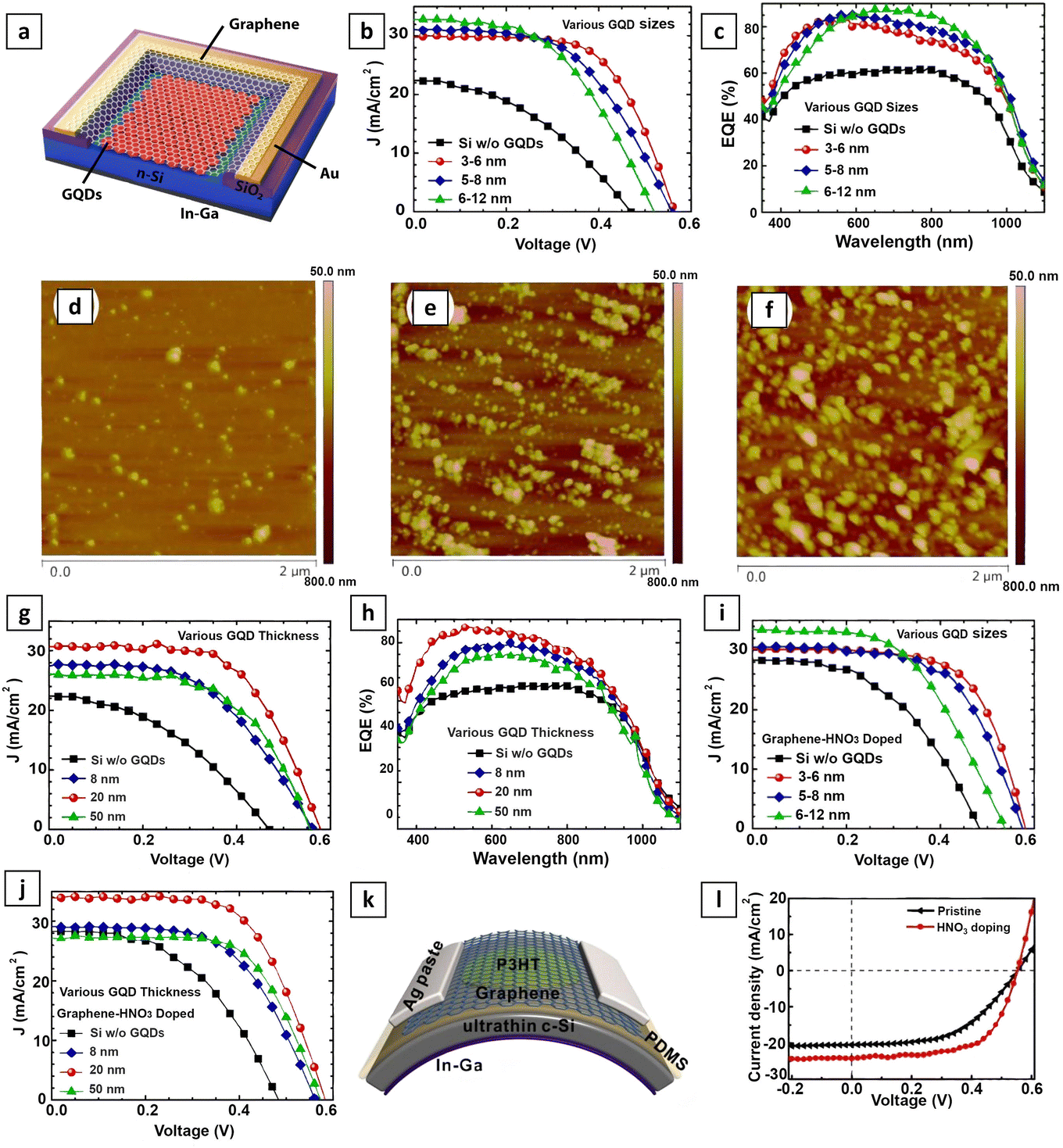 | ||
| Fig. 7 (a) Schematic diagram of the GQDs/Si device with Gr thin film. (b) and (c) J–V characteristics and EQE spectra of GQDs/Si devices manufactured with GQDs of various sizes. (d)–(f) AFM micrograph of GQDs film with different thicknesses of 8, 20, and 50 nm. (g) and (h) J–V characteristics and EQE spectra of GQDs/Si devices manufactured with GQDs of various thicknesses. (i) and (j) J–V characteristics of the GQDs/Si solar cell after HNO3 doping. Reproduced from ref. 113, with permission from Elsevier. (k) Schematic diagram of the flexible garphene/ultrathin c-Si solar cell. (l) J–V characteristics of solar cell with and without HNO3 doping. Reproduced from ref. 114, with permission from the Royal Society of Chemistry. | ||
 | ||
| Fig. 8 (a) The alteration of effective carrier lifetime of Si, Gr/Si, FG/Si and Gr/FG/Si samples estimated by microwave photo-induced conductance decay (MW-PCD). (b) The EQE spectra of Gr/Si and Gr/FG/Si solar cells. (c) The EQE spectra of device with HNO3 doping and TiO2 antireflection layer. Reproduced from ref. 115, with permission from Elsevier. (d) Schematic of the FLG plane Si solar cell in which the P3HT layer is sandwiched between the FLG film and Si substrate. (e) and (f) J–V characteristics and EQE spectra of 4-layer FLG-CH3-Si solar cells with various P3HT layer thicknesses. (g) and (h) J–V characteristics and EQE spectra of the FLG-CH3-Si solar cells with altered FLG layer numbers, the thickness of P3HT was set at 10 nm. Reproduced from ref. 116, with permission from the Royal Society of Chemistry. (i) J–V characteristics of pristine and HNO3 treatment, with and without a LiF interlayer. Reproduced from ref. 117, with permission from the Royal Society of Chemistry. | ||
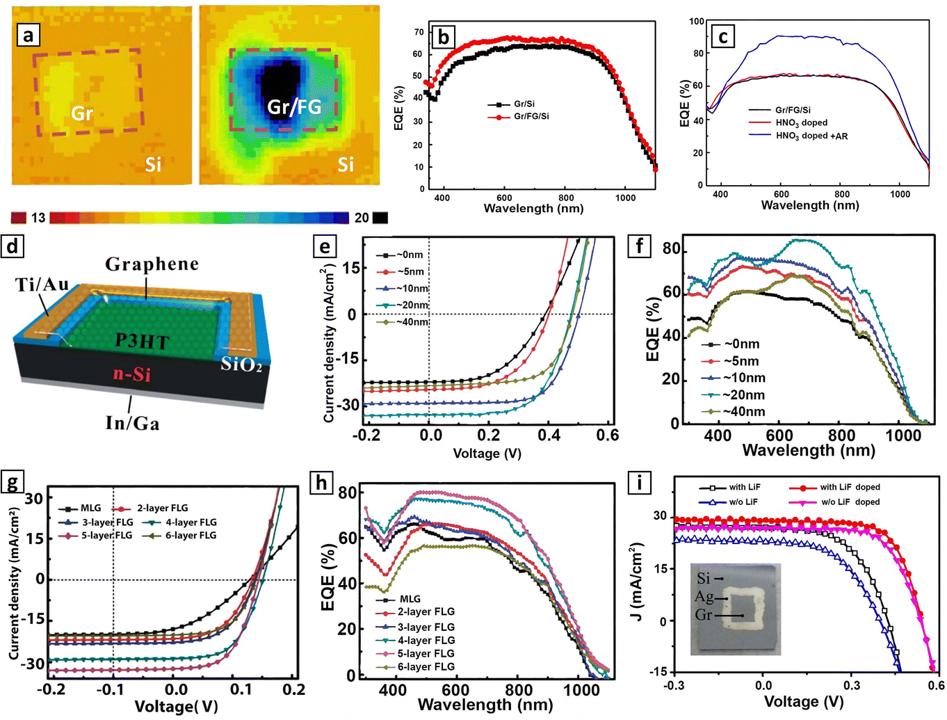
Zhong, Mengyao et al.115 proposed a one-stage strategy for doping and interface engineering of Gr/Si solar cells by employing the FG as an insulator interlayer. The carrier recombination of the device can be stifled at the front surface of Si via the FG interlayer. Fig. 8(a) illustrates the effective minority carrier lifetime (MCL) mapping of Gr/Si and Gr/FG/Si samples. The MCL of the Gr-deposited Si is approximately 16.2 μs. The Gr/FG solar cell deposited on Si, however, exhibits a considerably higher MCL (almost 20.6 μs). The boost of MCL can increase the external quantum efficiency (EQE) spectrum of the device, as depicted in Fig. 8(b). The clear boost of EQE at the short-wavelength range reflects the decline of carrier recombination. As a result, the power conversion efficiency (PCE) of the device improves from 3.17% to 7.52% with the application of the FG layer in the solar cell. Moreover, an enhancement is recorded in the PCE of the solar cell (13.38%) upon doping with HNO3 and TiO2 antireflection layer compared to the original solar cell (7.52%) (Fig. 8(a) and (b)).
Zhang et al. and Xie et al.116 reported the high-efficiency graphene-flat Si Schottky junction solar cells through modifying the Si surface with a molecule monolayer as well as interface band engineering with organic film (P3HT) to control electron distribution from n-Si to the graphene P3HT layer (Fig. 8(d)). The thickness of the P3HT layer was attentively managed by modifying the solution concentration. Various layer thicknesses were tested to reach the best performance of the Gr/Si solar cells and decrease the surface recombination. The best efficiency was obtained at the P3HT thickness of 10–20 nm, where, Jsc, Voc, FF, and PCE significantly improved from 21.85 mA cm−2, 0.38 V, 0.510, and 4.24% for the solar cell without a P3HT layer to 28.99 mA cm−2, 0.50 V, 0.669, and 9.70% for the solar cell with a P3HT layer (10 nm) (Fig. 8(e) and (f)). In addition, the highest PCE of graphene planar Si solar cells was achieved through additional optimization of the number of graphene layers and doping. They reported the optimal PCE of 10.56% in the system having 5-layer FLG-P3HT (10 nm)-CH3Si (Fig. 8(g) and (h)).
Xu, Dikai et al.117 used a lithium fluoride (LiF) layer as an insulator to stifle the recombination at the back surface and improve the hole blocking effect. The back contact resistance and series resistance of Gr–Si solar cells significantly declined, resulting in a remarkable rise in the power-conversion-efficiency (PCE) of devices.
As a consequence, the PCE of 6.25% was obtained for pristine Gr–Si solar cells. The highest value (10.61%) was recorded after HNO3 chemical doping (Fig. 8(i)).
4.2 Chemical doping of graphene surface
Doping of graphene is a promising strategy to enhance the efficiency of graphene/Si solar cells which can adjust its work function in addition to enhancing its electrical properties. The efficiency of solar cells can be effectively improved by different dopants such as polymers,118 Au nanoparticles,119 Ag-nanowires,120 Pt cubic nanoparticles,121 HNO3,122,123 SOCl2,124 triethylenetetramine (TETA),125 graphene oxide (GO),126,127 and bis (tri-fluoromethane sulfonyl) amide (TFSA).128Im, Min Ji et al.129 succeeded in heavy p-doping of the graphene layer via sandwich doping on both the top and bottom sides. The bottom side of the solar cell was doped by benzimidazole (BI) through etching while its top surface was doped with HAuCl4 solution (Fig. 9(a)). A monolayer of graphene was transferred by chemical vapor deposition (CVD). The sandwich-doping strategy boosted the work function to 5.07 eV, showing a 0.61 eV improvement compared to the pristine graphene device.
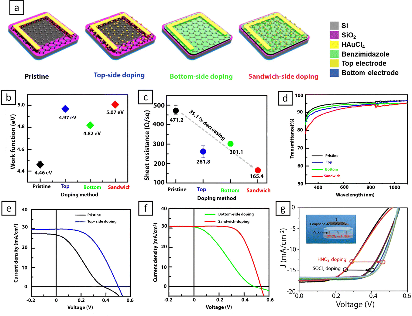 | ||
| Fig. 9 (a) Schematic diagram of the four types of the solar cell (pristine, top-side-doped, bottom-side-doped, and sandwich-doped graphene/silicon solar cells). (b) The work function. (c) Sheet resistance and (d) light transmittance of various doped graphene. (e) and (f) J–V characteristics of four types of the solar cell. Reproduced from ref. 129, with permission from American Chemical Society. (g) Light J–V characteristics of the solar cells (the inset shows the sample exposed to the SOCl2 and HNO3 vapor). Reproduced from ref. 130, with permission from the Royal Society of Chemistry. | ||
In addition, the sheet resistance of sandwich-doped graphene was 165.4 Ω sq−1, showing a 35.1% decline compared to the original graphene device. Thus, doping raised the conductivity (Fig. 9(b) and (c)). Fig. 10(d) compares the optical transmission of graphene devices in the wavelength range of 400–1000 nm. The optical transmittance values of pristine, top-surface-doped, bottom-surface-doped, and sandwich-doped graphene at 550 nm were 96.4%, 94.4%, 95.4%, and 93.1%, respectively. These modifications indicate slight light absorption by the adsorbed dopants. The sandwich-doping approach enhanced the work function of graphene at low RS with no notable decrease in optical transmittance (>90%). The power conversion efficiency of graphene–silicon solar cells having both sides-doped graphene was 10.02%, exhibiting a 334% enhancement compared to that of Schottky junction solar cells (SJSCs) (2.998%) composed of pristine graphene (Fig. 9(e) and (f)).
 | ||
| Fig. 10 (a) Schematics of graphene/n-Si solar cell and TFSA-doped solar cell. (b) J–V curves of the device. Reproduced from ref. 132, with permission from American Chemical Society. (c) Schematic design of Gr/P3HT/Si solar cell with two-layered antireflection coating. (d) Energy band structure of Gr/P3HT/Si solar cell. (e) J–V curves of the device after TFSA doping and an antireflection layer of TiO2/PDMS (illuminated for 1 hour). Reproduced from ref. 133, with permission from Wiley. (f) Schematic of the processes implicated in the fabrication of PFSA/HNO3/graphene/native oxide/Si solar cells. (g) J–V characteristics and (h) EQE spectra of the solar cell. Reproduced from ref. 135, with permission from Wiley. | ||
Xinming Li et al.130 examined the heavy p-type chemical doping by Thionyl chloride (SOCl2) and nitrate anions (HNO3) using a vapor technique. Their result indicated that doping improved the solar cell. Doping is a more effective strategy to decrease the sheet resistance and widen the work function of graphene for efficient charge separation and transport. The series resistance (Rs) of the solar cells declined from 54.41 to 47.43 Ω (a 13% drop) and from 49.58 to 26.84 U (a 46% decline), after SOCl2 and HNO3 treatments, respectively. Correspondingly, the solar energy conversion efficiency improved from 5.52% to 8.94% and 5.53% to 9.27% after SOCl2 and HNO3 doping. Therefore, nitrate ions were more useful for the chemical doping of graphene films compared to chlorine, as they decremented Rs, enhanced Voc and FF, and improved the conductivity of graphene layers, which also contributed to the improvement of the Schottky junction solar cells (Fig. 9(g)). Similarly, Cui et al.131 employed four volatile oxidants (HNO3, SOCl2, HCl, and H2O2) or improving the performance of devices. They put the formed graphene/Si solar cells above a vial having HNO3 (65 wt%), SOCl2 (99.5 wt%), HCl (36 wt%), or H2O2 (30 wt%) for 60 seconds.
The PCE was significantly improved after treatment by either of the four volatile oxidants. The result showed that SOCl2 doping led to the best PCE. A primary PCE (2.58%) of a solar cell (Voc = 412.10 mV, Jsc = 17.65 mA cm2, FF = 35.42%) could be raised to 5.95% (Voc = 547.78 mV, Jsc = 17.92 mA cm2, FF = 60.64%) after SOCl2 doping.
Concerning volatile oxidants, doping with organic polymer dopant bis-(trifluoromethanesulfonyl) amide TFSA is also an influential approach to enhancing the efficiency of graphene/Si solar cells. Miao et al.132 reported that TFSA could considerably improve the conductivity of graphene by p-doping (Fig. 10(a)). They indicated an enhancement in the PCE of the graphene/n-Si Schottky junction solar cell (8.6%) upon doping with TFSA compared to the original solar cell (1.9%) while the Jsc boosted from 14.2 to 25.3 mA cm2, Voc raised from 0.43 to 0.54 V (Fig. 10(b)).
Xu et al.133 reported high-performance Gr/n-type Si solar cells by employing a solution-processable poly(3-hexylthiophene-2,5-diyl) (P3HT) thin film placed between the Gr and n-type Si (n-Si) for doping the Gr layer (Fig. 10(c)). The large-surface monolayer graphene layers were deposited on a copper foil via the low-pressure chemical vapor deposition method. Fig. 10(d) illustrates a schematic energy band of the Gr/P3HT/Si solar cells. The large bandgap (≈2 eV)134 of P3HT does not affect sunlight transmission via the Gr/P3HT transparent cathode and contact with the n-Si (see Fig. 10(e)). The highest occupied molecular orbital of P3HT (−5.0 eV) is placed very near to the maximum of the valence band of n-Si (−5.17 eV), promoting the transport of photogenerated holes. The lowest unoccupied molecular orbital of P3HT (−3.0 eV) is considerably greater than the minimum value of the conduction band of n-Si (−4.05 eV), providing a large energy barrier for photoinduced electron transport to the Gr film. Such an electron blocking layer not only effectively reduces the leakage current but also greatly stifles the carrier recombination at the junction. In the case of light brightness, the photoinduced doping boosted the work function of Gr, thus, declining the energy band offset between Gr and P3HT, further modifying the Voc and FF of the device.
This layer boosted the work function and conductivity of the Gr layer, therefore, improving the Schottky barrier height of the device as the carrier recombination was quenched at the interface. This phenomenon can be attributed to photoinduced p-type (hole) doping under light illumination. After 1 hour of exposure to sunlight, the doping effect saturates and the PCE of Gr/P3HT/Si solar cells increased from 0.92% to 6.78%. The use of antireflection-based polydimethylsiloxane (PDMS) pyramid arrays, TiO2 nanoparticles, and also extra chemical doping (TFSA) on the opposite side of the Gr layer enhances the performance of Gr/P3HT/nSi solar cells, offering a power conversion efficiency of 12.95% with elevated stability (Fig. 10(e)).
Rehman, Malik Abdul et al.135 used acid-based graphene-Si macromolecular solar cells chemically doped with polymeric perfluorinated sulfonic acid (PFSA) macromolecules and nitric acid (HNO3) (Fig. 10(f)). They reported a high PCE of ∼9.27% with PFSA doping compared with an undoped device (7.64%). The highest PCE of 10.44% was achieved after co-doping with HNO3. PFSA macromolecular doping significantly declined the number of defects, made the graphene surface smooth and uniform, and effectively improved the open circuit voltage (Voc) from 0.500 to 0.521 V (Fig. 10(g) and (h)).
4.3 Control the reflectivity of silicon substrates via nano- and microstructure texturing and optical coating
Thanks to its significant reflectance, flat Si surfaces have a high absorption loss of 30–40% in the visible range.136 To improve light trapping, silicon substrates were designed with various nano and micro-textured structures such as pyramid texture,137–142 nanowires,143,144 nanopillars,145,146 and, a porous surface.147,148 The utilization of Si nano-or micro-textured can significantly improve light trapping ability due to the powerful light-collecting effect that stifles the reflection of the junction area in the visible and near-infrared range and enhances the light-collecting efficiency.149,150 Furthermore, a wide range of anti-reflection coatings (ARCs) such as TiO2,151,152 vanadium pentoxide (V2O5),153 PMMA,154,155 and PDMS156 can be utilized to reduce optical losses and increase the Jsc. However, it does not adversely affect other performance parameters of the solar cell. This strategy offers a promising way to fabricate highly efficient graphene/Si solar cells based on nano- or micro-textured Si.Lately, nano or microstructures have been extensively studied to improve the PCE of this type of solar cell. Therefore, the research works on the manufacturing of highly efficient nanostructured and microstructural graphene/Si solar cells are reviewed in this section. Recently, nanostructures or microstructures have been extensively studied to enhance the PCE of this type of solar cell.
For instance, Fan et al.157 used a silver-assisted etching process to fabricate silicon nanowire (SiNW) arrays; they deposited the graphene film onto the silicon nanowire (SiNW) array by a CVD method using nickel foils. According to Fig. 11(a)–(d) the SiNWs led to a remarkable decrease in reflectance. Upon irradiation, the graphene/SiNW solar cell showed a great photovoltaic response, accomplishing a PCE of 1.25% with a Voc, Jsc, and FF of 0.462 V, 9.2 mA cm−2, and 30%, respectively. Such a great response can be predominantly associated with two factors. The SiNWs offer an immediate and quick pathway to enhance the electrical hole collection and transport. Second, the SiNWs can increment light trapping and quench the reflection of the junction surface in the near-infrared range. Then, they used SOCl2 vapor to dope the graphene film to further increase the PCE of the solar cells to 2.86% (Fig. 11(e)).
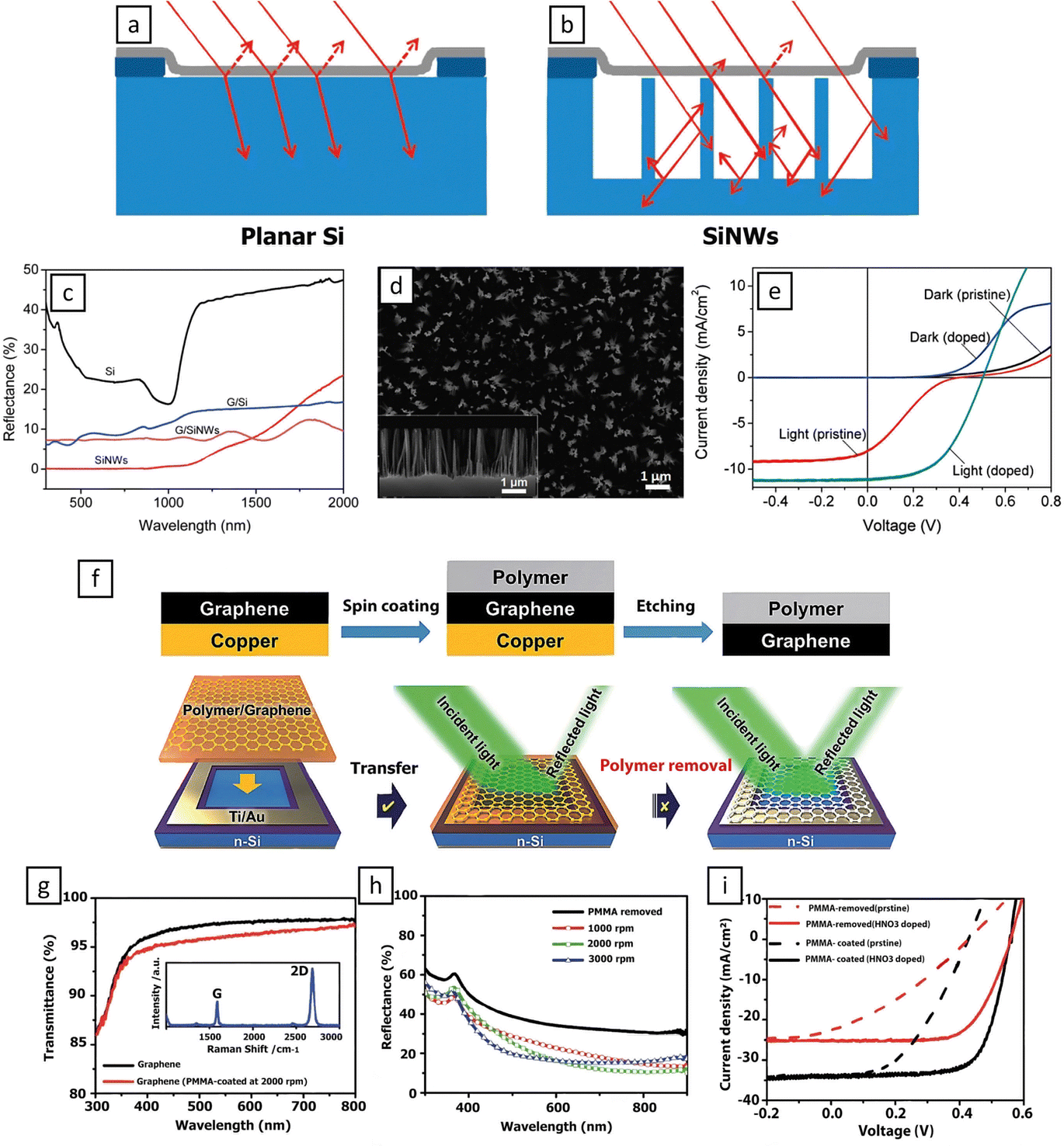 | ||
| Fig. 11 Schematics diagram of (a) Gr/flat Si and (b) Gr/SiNW junctions. (c) Reflectance spectra of flat Si, SiNWs, Gr/Si, and G/SiNWs. (d) SEM micrograph of SiNW array. (e) J–V characteristics of the G/SiNW device before and after chemical doping. Reproduced from ref. 157, with permission from American Chemical Society. (f) Schematic diagram of the polymer-deposited Gr/Si solar cells. (g) Transmittance spectra of PMMA-eliminated and PMMA-deposited (2000 rpm) graphene. (h) Reflectance spectra of PMMA-eliminated and PMMA-deposited graphene samples. (i) J–V characteristics of the PMMA-eliminated and PMMA-deposited Gr/Si solar cells before and after HNO3 doping. Reproduced from ref. 158, with permission from the Royal Society of Chemistry. | ||
Gun et al.158 reported a new approach by incorporating PMMA antireflection film into the Gr/Si solar cells. PMMA coatings generally serve as a protective layer in the graphene transfer process and are dismissed after the transfer process. But in this report, the PMMA was fixed on the graphene film and acted as an anti-reflection layer (Fig. 11(f)). Notably, the transmittance at 550 nm was estimated to be 96.0% with PMMA coatings. The antireflection effect of PMMA coating was also explored (Fig. 11(g) and (h)). The result indicates that the PCE of the HNO3-doped with the PMMA coating increased to 13.34% (Fig. 11(i)). The performance of graphene/Si solar cells with TiO2 was very lower than graphene/Si solar cells with PMMA coating.
Fallahazad et al.159 fabricated two types of rGO/Si solar cells to compare the effect of the flat silicon substrate and pyramidal silicon substrate on the performance of the final device (Fig. 12(a)). In this work, the reduced graphene oxide (rGO) layers were transferred on the pyramidal silicon substrate by the electrophoretic deposition (EPD) method. The EPD technique offers proper thickness control of the graphene layer at reasonable costs. Fig. 12(b) displays the FESEM micrographs of graphene layers on a pyramidal Si substrate. The outcomes demonstrated a decline in the reflectance of pyramidal silicon substrate from 23% to 14% in flat silicon substrate due to the increased light paths in different directions (Fig. 12(c)). The J–V characteristic curve of rGO/flat Si solar cells showed an open-circuit voltage (Voc) value of 0.35 V and a Jsc value of 4.32 mA cm−2, corresponding to efficiency (η) of 0.94%. The Voc, Jsc, and η of rGO/pyramidal Si are 0.37 V, 7.54 mA cm−2, and 1.76%, respectively (Fig. 12(d)). The enhancement in Voc and Jsc of rGO/pyramidal Si solar cell can be assigned to the light entrapment which led to a remarkable efficiency improvement. Furthermore, this enhancement can be also attributed to the inferior series resistance and elevated shunt resistance.
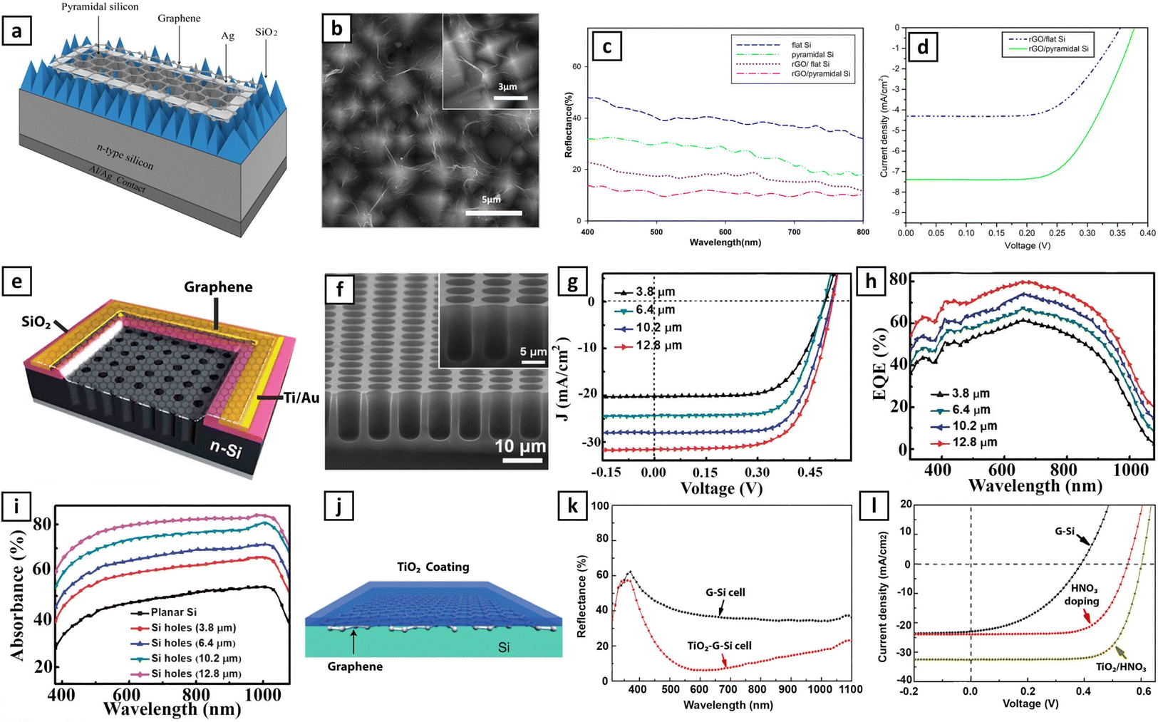 | ||
| Fig. 12 (a) Schematic structure of rGO/pyramidal Si solar cell. (b) FE-SEM images of the graphene layer on the pyramidal Si. (c) Reflection spectra of rGO on planner and pyramidal Si substrates. (d) J–V curves of the devices based on planner and pyramidal Si substrates. Reproduced from ref. 159, with permission from Elsevier. (e) Schematic diagram of the graphene/SiHA solar cell. (f) SEM images of SiHA sample. (g) and (h) J–V curves and EQE spectra of the graphene/SiHA solar cells with different hole depths. (i) Absorption spectra of the sample with different hole depths. Reproduced from ref. 160, with permission from The Royal Society of Chemistry. (j) Schematic illustration of the TiO2–Gr–Si solar cell. (k) Optical reflectance of a Gr/Si solar cell before and after TiO2 coating. (l) J–V curves of a Gr/Si solar cell recorded in the initial state (without coating), after HNO3 treatment, and after combined TiO2 layer deposition and HNO3 doping. Reproduced from ref. 161, with permission from American Chemical Society. | ||
Xie et al.160 investigated the structure of the graphene/microhole array (SiHA) device in terms of functionality and stability (Fig. 12(e)). They used photolithography and reactive ion etching (RIE) to achieve soft textured microhole arrays and controlled etching. They also employed a chemical vapor deposition (CVD) method for coating graphene layers. They manufactured graphene/microhole array (SiHA) devices with different hole depths. Fig. 12(f) shows the SEM image of SiHA. The improvement in the Jsc and EQE (external quantum efficiency) can be assigned to the improved optical absorption of the SiHA due to its deeper holes (Fig. 12(g) and (h)). According to their results, the optimal hole depth in SiHA was 12.8 μm due to the significant improvement of both current and voltage (Fig. 12(g)). Moreover, the best EQE of graphene/microhole array (SiHA) device was 80% at 680 nm as a result of the optimal hole depth of 12.8 μm (Fig. 12(h)). The thick SiHA (12.8 μm) exhibited the maximum effective optical absorption (above 80%) at the wavelength range of 400–1000 nm (Fig. 12(i)). Increasing the hole depth to 12.8 μm significantly improved the light capturing ability of the solar cells. The combination of the micro-hole array with AuCl3 doping enhanced the PCE to 10.4%. Further, the mentioned system exhibited excellent stability and high efficiency even after 3 months of exposure to air. Concerning stability, nano or microstructures can be viable candidates for efficient graphene/Si solar cells.
Shi et al.161 used TiO2 as an antireflection layer in a solar cell configuration comprising an n-Si substrate at the bottom and a TiO2 layer on the top sandwiching graphene. The mentioned system was achieved by the CVD method (Fig. 12(j)). Upon the deposition of TiO2 colloidal solution on the active surface of the graphene/Si solar cell to shape a soft layer, the reflectance in 500–800 nm was decreased to ∼10% (Fig. 12(k)). Also, the Jsc was enormously boosted from 23.9 to 32.5 mA cm−2 after TiO2 deposition. The resulting HNO3-doped TiO2/graphene/Si solar cell indicated a Voc of 0.60 V, a FF of 73%, and an efficiency of 14.1% (Fig. 12(l)). The Voc and FF enhancement can be ascribed to HNO3 doping, while the Jsc enhancement is related to TiO2 coating. By optimizing two parameters (Jsc and Voc), the PCE of graphene/Si solar cells reached 14.1%. The device lost its stability after doping as its efficiency extremely declined from 14.1% to 6.5% after 20 days in the ambient air. Nevertheless, the TiO2-induced antireflection properties ideally maintained the Jsc at almost 32 mA cm−2 during the mentioned period. They re-doped the device by HNO3 vapor, and the efficiency of the re-doped solar cell reached 14.5%, higher than that of previous records.
Ding et al.162 manufactured a multi-color Gr/Si solar cell based on MgF2/ZnS antireflection layer and extremely thin and highly transparent graphene. The maximum refractive index of ZnS is almost 2.5, while the minimum refractive index of MgF2 is 1.4. Hence, the MgF2/ZnS double film can act as an effective anti-reflection layer for solar cell devices. In this research, MgF2/ZnS was sequentially deposited on the graphene/Si solar cell by the thermal evaporation method. Different structural colors can be reached with accuracy by tuning the thickness of the films. The multi-color Gr/Si PV devices indicated acceptable power conversion efficiency (PCE) in the range of 10.7–13.2%, which is related to the color of the devices. Therefore, by optimizing the MgF2/ZnS anti-reflection layer, the PCE of the device can rise to 14.6%. Their results indicated the significant potential of colorful Gr/Si solar cells for high-efficiency and low-cost PV modules.
Kim et al.163 manufactured graphene/Si Schottky junction solar cells based on a porous silicon substrate (Fig. 13(a)). The target of their work was to enhance the optical absorption and electrical properties of the device with porous silicon. For this purpose, porous silicon was formed by metal-assisted chemical etching. Various deposition times (td) (1 to 7 s) were adopted for the etching of silicon substrate. Fig. 13(b) illustrates the energy band diagram of the graphene/PSi/n-Si junction. We suppose that the Fermi level of PSi resides at the middle of the bandgap regardless of the doping level of the starting silicon. The fact that the pores are mainly formed at the spots of Si defects and dopants during MacEtch164 causes an effective decrease in the doping concentration. The bandgap energy of porous silicon is larger than that of flat silicon due to the quantum confinement in Si nanostructures.165,166 The results indicated that a maximum PCE of 3.52% can be obtained by the deposition time (td) of 5 s for the etching of silicon substrate (Fig. 13(c)–(e)). Co-doping with Au NPs and TFSA was also utilized to improve the PCE of the solar cells from 3.52% to 10.69%. The co-doping sufficiently improved the work function of graphene and reduced sheet resistance of graphene compared to single-doping (Au NPs or TFSA) which was efficient for separating and collecting the photo-induced electron–hole pairs in the solar cells (Fig. 13(f)).
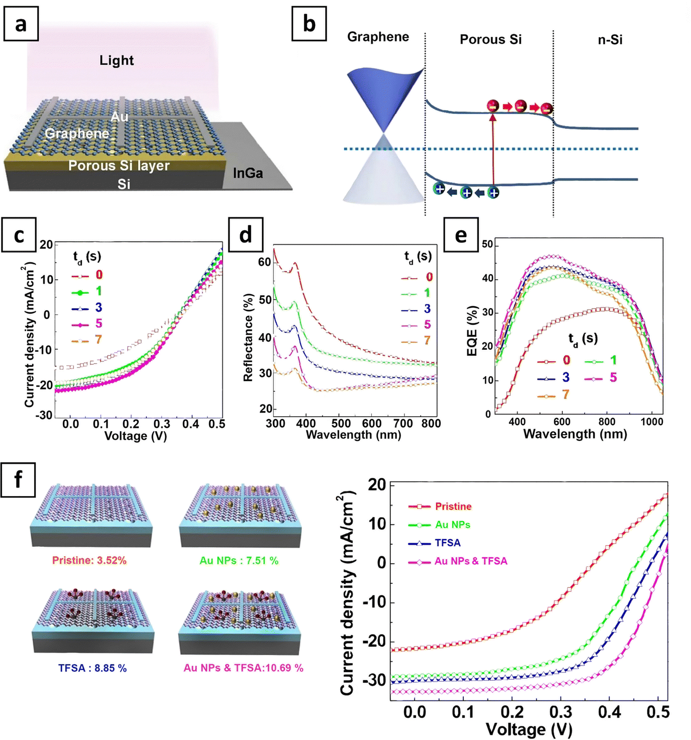 | ||
| Fig. 13 (a) Schematic illustration of graphene/PSi/n-Si solar cell with Au top contact and InGa bottom contact. (b) Energy band diagrams of the device. (c)–(e) J–V characteristics, reflectance, and EQE spectra of the devices with td from 0 to 7 s. (f) J–V characteristics, and (d) EQE spectra of the pristine, individually doped (Au NPs or TFSA), and co-doped graphene layers/PSi solar cells. Reproduced from ref. 163, with permission from the Royal Society of Chemistry. | ||
4.4 Controlled functionalization of the graphene layers and thickness
While chemical doping and interface engineering are effective strategies to improve the efficiency of the Gr/Si solar cells, the results also suggest the vital role of the number of graphene layers in enhancing the performance of solar cells. The controlled functionalization of the graphene layer can effectively adjust its work function and sheet resistance, hence, incrementing the barrier height of the junction. The single-layer graphene has a high sheet resistance, but increasing the number of graphene layers declines the sheet resistance while affecting its transparency. Thus, the sheet resistance should be optimized by controlling the number of graphene layers without losing transparency. In addition, the optimization of thickness is a key factor in enhancing the performance of graphene-based solar cells. The Gr/Si junction is much thinner than a regular p–n junction solar cell, thus, the work function and efficiency can be remarkably enhanced by controlling the thickness of graphene.The effect of the thickness of the graphene layer on the PCE of graphene/Si solar cells has been also investigated. Rehman, Malik Abdul et al.167 reported that carrier recombination is diminished by optimizing the thickness of the graphene layer. They altered the thickness of the layer from 2 nm to 4 nm, and 8 nm by prolonging the deposition time from 2.5 to 3.5 and 4.5 h, respectively (Fig. 14(a)). The result showed a high PCE of 5.51% for the 4 nm-thick graphene device deposited on bare flat silicon (Fig. 14(b)). Moreover, the efficiency is strangely increased to 9.18% upon the deposition of PMMA and doping with HNO3. Therefore, the smooth area of direct deposition of graphene and adjustment of the thickness of carbon with rising growth time was confirmed.
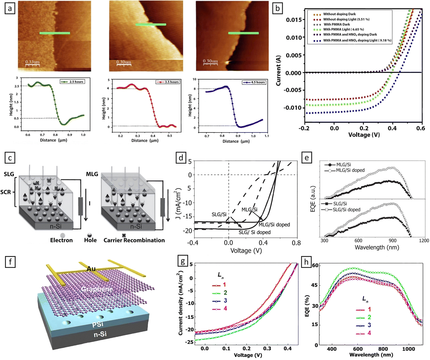 | ||
| Fig. 14 (a) AFM micrograph to illustrate various thicknesses of graphene directly grown for different growth durations. (b) J–V curves of optimized thickness graphene layer under light and dark, with the PMMA layer and with HNO3 doping. Reproduced from ref. 167, with permission from Elsevier. (c) Schematic demonstration of the split and recombination of carriers at the interface of SLM/Si and MLG/Si. (d) J–V characteristics and (e) EQE spectra of SLG/Si and MLG/Si solar cells before and after doping. Reproduced from ref. 169, with permission from Wiley. (f) Schematic illustration of graphene/PSi solar cells. (g) J–V characteristics, and (h) EQE spectra of graphene/PSi/n-Si solar cells with various Ln values (from 1 to 4). Reproduced from ref. 170, with permission from American Institute of Physics. | ||
According to ref. 168 the photovoltaic characteristics of the graphene/Si solar cells can be improved by incrementing the number of graphene layers. The result showed a steady enhancement of the PCE and short circuit current of the solar cell for less than 4 graphene layers. The mentioned parameters showed a decline when the number of graphene layers exceeded 4. The decrease in PCE is thought to be due to a decrement in the graphene permeability for more than 5 layers. Thus, the 4-layer graphene is a superlative promising material for the development of high-performance Schottky junction solar cells. The PCE of the 4-layer graphene solar cell can be enhanced by further alteration of the graphene sheet resistance and the series resistance of the devices through chemical doping.
Xinming Li et al.169 reported the extremely superior solar conversion capacity of multilayer graphene films despite their lower transparency and conductivity compared to their monolayer counterparts. The multi-layer graphene leads to a reasonable junction compared to single-layer graphene and stifles the recombination at the junction (Fig. 14(c)). Chemical doping with acid remarkably improved the conversion efficiency of the MLG/Si device from 4.98% to 9.63% due to the enhancement in charge separation and transport. Doping also improved the efficiency of the SLG/Si device but not as high as the doped MLG/Si device (Fig. 14(d) and (e)). In another report, Shin et al.170 examined the effect of layer number (Ln) of graphene on the efficiency of graphene/PSi solar cells due to its direct association with the efficiency of graphene/PSi solar cells (Fig. 14(f)). In general, the sheet resistance, work function, transmittance, and reflectance of graphene highly depend on Ln. The most considerable PCE of 4.35% was achieved for Ln = 2 in the pristine graphene/PSi/n-Si solar cell. Several metal chlorides were employed as dopants in MLG at Ln = 2 to promote and enhance the efficiency of the solar cells (Fig. 14(g) and (h)). The RhCl3-doped graphene/PSi solar cell offered the maximum PCE of 9.15% due to its considerable work function and relatively small sheet resistance.
4.5 III–V semiconductors for interfacial graphene
To exploit the new interface science to realize highly efficient and stable graphene-based solar cells, graphene layers are not only combined with Si, but also with other inorganic semiconductors such as III–V semiconductors with a direct band gap (e.g. gallium arsenide (GaAs), gallium nitride (GaN), and indium phosphide (InP)). Thanks to the large direct bandgap of III–V semiconductors their heterojunctions with graphene may result in higher built-in potentials. Li Xiaoqiang et al.171 reported the graphene/GaAs solar cell encompassing SiNx film sandwiched between graphene layer and GaAs substrate as the dielectric insulating layer (Fig. 15(a)). The number of graphene layers on the GaAs substrate was examined. Accordingly, the Voc decreased by increasing the number of graphene layers. The highest PCE (9.20%) was achieved in tri-layer graphene. Monolayer graphene absorbs more than 2% of the incident light, thus, one more layer of graphene will make more than a 2% decline in Jsc. The fill factor of solar cell is generally under the influence of series resistance; such that the series resistance decrease by enhancing the number of graphene layers, leading to higher FF (Fig. 15(b)–(e)). Further enhancement of PCE can be achieved by increasing Jsc through the use of the Al2O3 antireflection layer on graphene. The use of the ARC layer lead to ∼30% enhancement in Jsc compared to the solar cell without an ARC layer. The highest PCE (15.5%) was obtained with TFSA doping and ARC (Fig. 15(f)). In another study, Li, Xiaoqiang et al.172 developed a graphene/GaAs heterostructure solar cell using an Al2O3 antireflection coating (ARC) layer and bis(trifluoromethanesulfonyl)amide [((CF3SO2)2NH)] (TFSA) as a dopant. The resulting system offered a high conversion efficiency of 15.5%.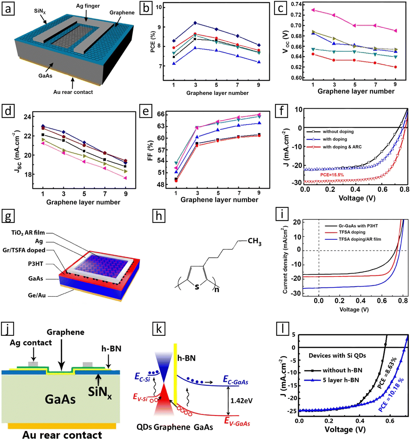 | ||
| Fig. 15 (a) Schematic configuration of the graphene/GaAs solar cell, Five groups of characteristic (b) PCE, (c) Voc, (d) Jsc, and (e) FF of the devices with various numbers of graphene layers. (f) J–V characteristics of the devices. Reproduced from ref. 171, with permission from Elsevier. (g) Schematic diagram of the TiO2-coated Gr-P3HT-GaAs solar cell after TFSA doping. (h) The structure of P3HT. (i) J–V characteristics of the Gr-P3HT-GaAs solar cell recorded in the initial state with TFSA doping and with TFSA doping/AR film. Reproduced from ref. 173, with permission from Elsevier. (j) Energy band diagrams of the graphene/h-BN/GaAs solar cell with Si QDs. (l) Schematic illustration of the graphene/h-BN/GaAs solar cell. (k) J–V characteristics of devices with Si QDs presented photo-induced doping. Reproduced from ref. 174, with permission from ref. 174©The Optical Society. | ||
He Hang et al.173 developed a highly-efficient GaAs/graphene solar cell by modifying the interface of the device with poly(3-hexylthiophene) (P3HT) as a hole transport layer (Fig. 15(g) and (h)). The Voc and Jsc of the device showed an increment due to the presence of the P3HT layer. Such an improvement can be assigned to the rise of the built-in barrier and the decrease in the carrier recombination at the Gr–GaAs junction. A Primary PCE of 6.84% can be achieved for the Gr–GaAs solar cell with a P3HT layer. Moreover, TiO2 anti-reflective film and chemical doping by bis (trifluoromethanesulfonyl)-amide were also employed in the device with a P3HT layer, which led to the PCE of 13.7% (Fig. 15(i)).
Li Xiaoqiang et al.174 compared the power conversion efficiency (PCE) of graphene/h-BN/GaAs with graphene/GaAs structure (Fig. 15(j)). The barrier height of graphene/GaAs heterojunction can be improved by the use of h-BN due to the improvement of Fermi level adjustment effect through the h-BN interface. Moreover, the h-BN layer can quench the static charge transfer process. Fig. 15(k) indicates the electronic band diagram and charge transfer of the Si QDs doped graphene/h-BN/GaAs solar cell. The PCE of the graphene/GaAs heterojunction is 6.51% which rose to 7.10% in the graphene/h-BN/GaAs structure with 5 layers of h-BN. Upon photo-induced doping into the heterojunction, the PCE of 10.18% was obtained in graphene/h-BN/GaAs compared to 8.63% of graphene/GaAs structure (Fig. 15(l)).
5. Summary and future outlook
The recent improvement strategies of graphene/silicon solar cells were reviewed in this article. Regarding the findings of the continuous works in this field, Gr/Si solar cells appear to be a promising new technology for upcoming solar cells. Despite rapid advances, there are limitations and challenges in the development of high-efficiency graphene-based solar cells. Thus, several strategies have been expanded to optimize the efficiency of solar cells. The work function, sheet resistance, and optical transparency of graphene can be regulated by adjusting the number of layers, chemical doping, photo-induced doping, or electric field-effect to increment the carrier concentration, barrier height, series resistance, and optical absorption of the photovoltaic system. Device barrier height and optical carrier recombination rate can be enhanced via interface band engineering to adjust the band alignment and interface passivation, saturate the dangling bonds, and decrease interface defects. Light absorption can be improved through the incorporation of semiconductor nano/micro-structures, antireflection layers, or plasmonic nanostructures. The conversion efficiency of graphene-based solar cells can be improved by adopting combinational strategies. Some reports discussed the influence of both the textured silicon substrate and the number of graphene layers. In the case of the Gr/porous Si solar cell, the cell efficiency increased due to the optimization of the graphene layer. Moreover, the light absorption of the solar cell showed a significant increase due to the surface texture. Therefore, the combination of dielectric surface passivation layers and anti-reflection layer seems to improve photovoltaic performance. For instance, aluminum oxide (Al2O3) and MoS2 can decrease the recombination at the junction. Therefore, a combination of a MoS2 interfacial layer and a TiO2 antireflection layer can dramatically improve the performance of Solar cells. In addition, various inorganic semiconductors such as GaAs have shown excellent potential for enhancing solar cell efficiency.Given the history of Gr/Si solar cells, we highlight some suggestions and an effective approach to possible PCE improvements, which should be taken into consideration for the future development of Gr/Si solar cells. The Gr/Si solar cells are yet to suffer from the shortage of passivation techniques. In contrast, different surface passivation techniques have been broadly studied for traditional p–n junction solar cells, such as passivated emitter and rear cell (PERC), passivated emitter, and rear locally-doped (PERL). Therefore, this is a practical and the most suitable scenario that will significantly improve graphene solar cells in the future. Passivation strategies and materials with higher efficiency can be employed to the rear contact of Gr/Si solar cells. More effective passivation material such as silicon nitride can be employed for the rear contact of Gr/Si solar cells. However, it is worth noting that the thickness of the passivation layer should be optimized because a supremely thin film may not be sufficient for effective passivation, while a considerably thick film would impede the efficient collection of carriers.
On the other hand, since the PCE of solar cells is restricted by the recombination of carriers, a silicon substrate with a longer lifetime would be expected to improve the efficiencies. Within this context, an investigation of the impact of silicon doping concentration on Gr/Si solar cell efficiency can be helpful to improve the Gr/Si junction construction. Another approach focuses on the device area, which could be further boosted by combining nano and micro-textured silicon, as a promising way to improve the PCE of Gr/Si solar cells in the future. However, there have been no reports on this strategy so far. Pyramidal silicon alongside porous silicon is an appropriate structure that can act as an antireflective layer to resolve the problem of the high reflection coefficient in the silicon substrates. In general, the PCE of Gr/Si is still low compared to conventional p–n junction solar cells; however, it is interesting and worth noting that the laboratory PCE of graphene-based silicon solar cells is ∼18%. Furthermore, under ideal conditions and based on theory, the efficiency limits of graphene/silicon and graphene/GaAs solar cells are expected to be 25.5% and 27.5%, respectively.175 Therefore, an obvious outlook can be predicted according to percentages obtained from the theoretical findings. In conclusion, the PCE of graphene/silicon solar cells would be further elevated to a superior record if whole performance engineering is contained and manufacturing quality can be improved.
Conflicts of interest
There are no conflicts to declare.Acknowledgements
We are grateful to Dr Mohamad Javad Eshraghi for his guidance.References
- D. Higgins, P. Zamani, A. Yu and Z. Chen, The application of graphene and its composites in oxygen reduction electrocatalysis: a perspective and review of recent progress, Energy Environ. Sci., 2016, 9, 357–390 RSC.
- D. W. Chang and J. B. Baek, Nitrogen-Doped Graphene for Photocatalytic Hydrogen Generation, Asian J. Chem., 2016, 11, 1125–1137 CrossRef CAS PubMed.
- K. Yoshikawa, H. Kawasaki, W. Yoshida, T. Irie, K. Konishi, K. Nakano, T. Uto, D. Adachi, M. Kanematsu and H. Uzu, Silicon Heterojunction Solar Cell with Interdigitated Back Contacts for a Photoconversion Efficiency over 26%, Nat. Energy, 2017, 2, 1–8 Search PubMed.
- S. Pizzini, M. Acciarri and S. Binetti, From Electronic Grade to Solar Grade Silicon: Chances and Challenges in Photovoltaics, Phys. Status Solidi A, 2005, 202, 2928–2942 CrossRef CAS.
- J. Jean, P. R. Brown, R. L. Jaffe, T. Buonassisi and V. Bulović, Pathways for Solar Photovoltaics, Energy Environ. Sci., 2015, 8, 1200–1219 RSC.
- H. Zhu, J. Wei, K. Wang and D. Wu, Applications of Carbon Materials in Photovoltaic Solar Cells, Sol. Energy Mater. Sol. Cells, 2009, 93, 1461–1470 CrossRef CAS.
- X. Li, Z. Lv and H. Zhu, Carbon/Silicon Heterojunction Solar Cells: State of the Art and Prospects, Adv. Mater., 2015, 27, 6549–6574 CrossRef CAS PubMed.
- A. K. Geim and K. S. Novoselov, The Rise of Graphene, Nat. Mater., 2007, 6, 183–191 CrossRef CAS PubMed.
- T. Mahmoudi, Y. Wang and Y.-B. Hahn, Graphene and Its Derivatives for Solar Cells Application, Nano Energy, 2018, 47, 51–65 CrossRef CAS.
- T. W. Ebbesen and P. M. Ajayan, Large-Scale Synthesis of Carbon Nanotubes, Nature, 1992, 358, 220–222 CrossRef CAS.
- T. Dürkop, S. A. Getty, E. Cobas and M. Fuhrer, Extraordinary Mobility in Semiconducting Carbon Nanotubes, Nano Lett., 2004, 4, 35–39 CrossRef.
- D. D. Tune, N. Mallik, H. Fornasier and B. S. Flavel, Breakthrough Carbon Nanotube–Silicon Heterojunction Solar Cells, Adv. Energy Mater., 2020, 10, 1903261 CrossRef CAS.
- Y. Jia, A. Cao, X. Bai, Z. Li, L. Zhang, N. Guo, J. Wei, K. Wang, H. Zhu and D. Wu, Achieving High Efficiency Silicon–Carbon Nanotube Heterojunction Solar Cells by Acid Doping, Nano Lett., 2011, 11, 1901–1905 CrossRef CAS PubMed.
- S. Mahalingam, A. Manap, K. Lau, A. Omar, P. Chelvanathan, C. Chia, N. Amin, I. Mathews, N. Afandi and N. Rahim, Mixture deposition method for graphene quantum dots-based dye-sensitized solar cell, Electrochim. Acta, 2022, 404, 139732 CrossRef CAS.
- Y. Zhu, S. Murali, W. Cai, X. Li, J. W. Suk, J. R. Potts and R. S. Ruoff, Graphene and graphene oxide: synthesis, properties, and applications, Adv. Mater., 2010, 22, 3906–3924 CrossRef CAS PubMed.
- Y. Li, N. An, Z. Lu, Y. Wang, B. Chang, T. Tan, X. Guo, X. Xu, J. He and H. Xia, Nonlinear co-generation of graphene plasmons for optoelectronic logic operations, Nat. Commun., 2022, 13, 1–7 Search PubMed.
- K. S. Kim, Y. Zhao, H. Jang, S. Y. Lee, J. M. Kim, K. S. Kim, J.-H. Ahn, P. Kim, J.-Y. Choi and B. H. Hong, Large-scale pattern growth of graphene films for stretchable transparent electrodes, Nature, 2009, 457, 706–710 CrossRef CAS PubMed.
- G. Eda, G. Fanchini and M. Chhowalla, Large-area ultrathin films of reduced graphene oxide as a transparent and flexible electronic material, Nat. Nanotechnol., 2008, 3, 270–274 CrossRef CAS PubMed.
- J. C. Meyer, A. K. Geim, M. I. Katsnelson, K. S. Novoselov, T. J. Booth and S. Roth, The structure of suspended graphene sheets, Nature, 2007, 446, 60–63 CrossRef CAS PubMed.
- Y. Xu, H. Bai, G. Lu, C. Li and G. Shi, Flexible graphene films via the filtration of water-soluble noncovalent functionalized graphene sheets, J. Am. Chem. Soc., 2008, 130, 5856–5857 CrossRef CAS PubMed.
- X. Zhou and Z. Liu, A scalable, solution-phase processing route to graphene oxide and graphene ultralarge sheets, Chem. Commun., 2010, 46, 2611–2613 RSC.
- Y.-W. Son, M. L. Cohen and S. G. Louie, Half-metallic graphene nanoribbons, Nature, 2006, 444, 347–349 CrossRef CAS PubMed.
- M. Y. Han, B. Özyilmaz, Y. Zhang and P. Kim, Energy band-gap engineering of graphene nanoribbons, Phys. Rev. Lett., 2007, 98, 206805 CrossRef PubMed.
- T. Chen and L. Dai, Macroscopic Graphene Fibers Directly Assembled from CVD-Grown Fiber-Shaped Hollow Graphene Tubes, Angew. Chem., Int. Ed., 2015, 127, 15160–15163 CrossRef.
- Y. Li, Q. Peng, X. He, P. Hu, C. Wang, Y. Shang, R. Wang, W. Jiao and H. Lv, Synthesis and characterization of a new hierarchical reinforcement by chemically grafting graphene oxide onto carbon fibers, J. Mater. Chem., 2012, 22, 18748–18752 RSC.
- H. Chen, M. B. Müller, K. J. Gilmore, G. G. Wallace and D. Li, Mechanically strong, electrically conductive, and biocompatible graphene paper, Adv. Mater., 2008, 20, 3557–3561 CrossRef CAS.
- F. Bonaccorso, Z. Sun, T. Hasan and A. Ferrari, Graphene photonics and optoelectronics, Nat. Photonics, 2010, 4, 611–622 CrossRef CAS.
- K. Jiao, D. Zhang and Y. Chen, Efficient and cost-effective graphene on silicon solar cells prepared by spray coating, RSC Adv., 2014, 4, 55300–55304 RSC.
- X.-G. Hu, Q. Wei, Y.-M. Zhao, P.-X. Hou, W. Ren, C. Liu and H.-M. Cheng, FeCl 3-functionalized graphene oxide/single-wall carbon nanotube/silicon heterojunction solar cells with an efficiency of 17.5%, J. Mater. Chem. A, 2022, 10, 4644–4652 RSC.
- M. Gürsoy, E. Çıtak and M. Karaman, Uniform deposition of large-area graphene films on copper using low-pressure chemical vapor deposition technique, Carbon Lett., 2022, 32, 781–787 CrossRef.
- B. Fallahazad, K. Lee, G. Lian, S. Kim, C. Corbet, D. Ferrer, L. Colombo and E. Tutuc, Scaling of Al2O3 dielectric for graphene field-effect transistors, Appl. Phys. Lett., 2012, 100, 093112 CrossRef.
- N. Shang, P. Papakonstantinou, P. Wang and S. R. P. Silva, Platinum integrated graphene for methanol fuel cells, J. Phys. Chem. C, 2010, 114, 15837–15841 CrossRef CAS.
- H. Su and Y. H. Hu, Recent advances in graphene-based materials for fuel cell applications, Energy Sci. Eng., 2021, 9, 958–983 CrossRef CAS.
- J. J. Yoo, K. Balakrishnan, J. Huang, V. Meunier, B. G. Sumpter, A. Srivastava, M. Conway, A. L. Mohana Reddy, J. Yu and R. Vajtai, Ultrathin planar graphene supercapacitors, Nano Lett., 2011, 11, 1423–1427 CrossRef CAS PubMed.
- S. Vivekchand, C. S. Rout, K. Subrahmanyam, A. Govindaraj and C. N. R. Rao, Graphene-based electrochemical supercapacitors, J. Chem. Sci., 2008, 120, 9–13 CrossRef CAS.
- Q. Li, X. Li, S. Wageh, A. A. Al-Ghamdi and J. Yu, CdS/graphene nanocomposite photocatalysts, Adv. Energy Mater., 2015, 5, 1500010 CrossRef.
- J. H. Choi, J. S. Seo, H. E. Jeong, K. Song, S.-H. Baeck, S. E. Shim and Y. Qian, Effects of field-effect and Schottky heterostructure on p-type graphene-based gas sensor modified by n-type In2O3 and phenylenediamine, Appl. Surf. Sci., 2022, 578, 152025 CrossRef CAS.
- H. J. Räder, A. Rouhanipour, A. M. Talarico, V. Palermo, P. Samorì and K. Müllen, Processing of giant graphene molecules by soft-landing mass spectrometry, Nat. Mater., 2006, 5, 276–280 CrossRef PubMed.
- K. Yang, L. Feng and Z. Liu, Stimuli responsive drug delivery systems based on nano-graphene for cancer therapy, Adv. Drug Delivery Rev., 2016, 105, 228–241 CrossRef CAS PubMed.
- Y. Xi, J. Zhuang, W. Hao and Y. Du, Recent Progress on Two-Dimensional Heterostructures for Catalytic, Optoelectronic, and Energy Applications, ChemElectroChem, 2019, 6, 2841–2851 CrossRef CAS.
- S. Ullah, X. Yang, H. Q. Ta, M. Hasan, A. Bachmatiuk, K. Tokarska, B. Trzebicka, L. Fu and M. H. Rummeli, Graphene Transfer Methods: A Review, Nano Res., 2021, 14, 3756–3772 CrossRef CAS.
- X. Li, W. Cai, J. An, S. Kim, J. Nah, D. Yang, R. Piner, A. Velamakanni, I. Jung and E. Tutuc, Large-Area Synthesis of High-Quality and Uniform Graphene Films on Copper Foils, Science, 2009, 324, 1312–1314 CrossRef CAS PubMed.
- H. A. Chaliyawala, N. Rajaram, R. Patel, A. Ray and I. Mukhopadhyay, Controlled island formation of large-area graphene sheets by atmospheric chemical vapor deposition: Role of natural camphor, ACS Omega, 2019, 4, 8758–8766 CrossRef CAS PubMed.
- F. Bonaccorso, L. Colombo, G. Yu, M. Stoller, V. Tozzini, A. C. Ferrari, R. S. Ruoff and V. Pellegrini, Graphene, related two-dimensional crystals, and hybrid systems for energy conversion and storage, Science, 2015, 347, 1246501 CrossRef PubMed.
- M. Sharifi, N. Naderi, P. Fallahazad and M. J. Eshraghi, Role of graphene on the optoelectrical stability of photodetectors based on porous silicon, Sens. Actuators, A, 2020, 310, 112065 CrossRef CAS.
- F. H. Koppens, D. E. Chang and F. J. García de Abajo, Graphene plasmonics: a platform for strong light–matter interactions, Nano Lett., 2011, 11, 3370–3377 CrossRef CAS PubMed.
- D. D. Tune and B. S. Flavel, Advances in Carbon Nanotube–Silicon Heterojunction Solar Cells, Adv. Energy Mater., 2018, 8, 1703241 CrossRef.
- K. Jiao, X. Wang, Y. Wang and Y. Chen, Graphene Oxide as an Effective Interfacial Layer for Enhanced Graphene/Silicon Solar Cell Performance, J. Mater. Chem. C, 2014, 2, 7715–7721 RSC.
- A. Lerf, H. He, M. Forster and J. Klinowski, Structure of graphite oxide revisited, J. Phys. Chem. B, 1998, 102, 4477–4482 CrossRef CAS.
- H. He, J. Klinowski, M. Forster and A. Lerf, A new structural model for graphite oxide, Chem. Phys. Lett., 1998, 287, 53–56 CrossRef CAS.
- W. Gao, L. B. Alemany, L. Ci and P. M. Ajayan, New insights into the structure and reduction of graphite oxide, Nat. Chem., 2009, 1, 403–408 CrossRef CAS PubMed.
- Z.-l Wang, D. Xu, Y. Huang, Z. Wu, L.-m Wang and X.-b Zhang, Facile, mild and fast thermal-decomposition reduction of graphene oxide in air and its application in high-performance lithium batteries, Chem. Commun., 2012, 48, 976–978 RSC.
- Y. Cao, Z. Xiong, F. Xia, G. V. Franks, L. Zu, X. Wang, Y. Hora, S. Mudie, Z. He and L. Qu, New structural insights into densely assembled reduced graphene oxide membranes, Adv. Funct. Mater., 2022, 2201535 CrossRef CAS.
- E. Singh and H. S. Nalwa, Stability of graphene-based heterojunction solar cells, RSC Adv., 2015, 5, 73575–73600 RSC.
- A. Mathkar, D. Tozier, P. Cox, P. Ong, C. Galande, K. Balakrishnan, A. Leela Mohana Reddy and P. M. Ajayan, Controlled, stepwise reduction and band gap manipulation of graphene oxide, J. Phys. Chem. Lett., 2012, 3, 986–991 CrossRef CAS PubMed.
- B. Liu, A. C. Neto, F. Guinea, N. M. Peres, K. S. Novoselov and A. K. Geim, The electronic properties of graphene, Rev. Mod. Phys., 2009, 81, 109 CrossRef.
- C. Bonavolontà, A. Vettoliere, G. Falco, C. Aramo, I. Rendina, B. Ruggiero, P. Silvestrini and M. Valentino, Reduced graphene oxide on silicon-based structure as novel broadband photodetector, Sci. Rep., 2021, 11, 1–10 CrossRef PubMed.
- R. R. Nair, P. Blake, A. N. Grigorenko, K. S. Novoselov, T. J. Booth, T. Stauber, N. M. Peres and A. K. Geim, Fine structure constant defines visual transparency of graphene, Science, 2008, 320, 1308 CrossRef CAS PubMed.
- G. Fiori, F. Bonaccorso, G. Iannaccone, T. Palacios, D. Neumaier, A. Seabaugh, S. K. Banerjee and L. Colombo, Electronics based on two-dimensional materials, Nat. Nanotechnol., 2014, 9, 768–779 CrossRef CAS PubMed.
- X. Wang, H. You, F. Liu, M. Li, L. Wan, S. Li, Q. Li, Y. Xu, R. Tian and Z. Yu, Large-scale synthesis of few-layered graphene using CVD, Chem. Vap. Depos., 2009, 15, 53–56 CrossRef CAS.
- S. Bae, H. Kim, Y. Lee, X. Xu, J.-S. Park, Y. Zheng, J. Balakrishnan, T. Lei, H. Ri Kim and Y. I. Song, Roll-to-roll production of 30-inch graphene films for transparent electrodes, Nat. Nanotechnol., 2010, 5, 574–578 CrossRef CAS PubMed.
- S. Pang, Y. Hernandez, X. Feng and K. Mullen, Adv. Mater., 2011, 23, 2779 CrossRef CAS PubMed.
- A. Di Bartolomeo, Graphene Schottky diodes: An experimental review of the rectifying graphene/semiconductor heterojunction, Phys. Rep., 2016, 606, 1–58 CrossRef CAS.
- T. Saga, Advances in crystalline silicon solar cell technology for industrial mass production, NPG Asia Mater., 2010, 2, 96–102 CrossRef.
- T.-H. Han, Y. Lee, M.-R. Choi, S.-H. Woo, S.-H. Bae, B. H. Hong, J.-H. Ahn and T.-W. Lee, Extremely efficient flexible organic light-emitting diodes with modified graphene anode, Nat. Photonics, 2012, 6, 105–110 CrossRef CAS.
- Y. Lin, X. Li, D. Xie, T. Feng, Y. Chen, R. Song, H. Tian, T. Ren, M. Zhong and K. Wang, Graphene/semiconductor heterojunction solar cells with modulated antireflection and graphene work function, Energy Environ. Sci., 2013, 6, 108–115 RSC.
- E. Shi, L. Zhang, Z. Li, P. Li, Y. Shang, Y. Jia, J. Wei, K. Wang, H. Zhu and D. Wu, TiO2-coated carbon nanotube-silicon solar cells with efficiency of 15%, Sci. Rep., 2012, 2, 1–5 Search PubMed.
- X. Li, H. Zhu, K. Wang, A. Cao, J. Wei, C. Li, Y. Jia, Z. Li, X. Li and D. Wu, Graphene-on-silicon Schottky junction solar cells, Adv. Mater., 2010, 22, 2743–2748 CrossRef CAS PubMed.
- S. Chandramohan, S. Durairaj, T. H. Seo, B. D. Ryu and C.-H. Hong, Observation of dopant-dependent efficiency in chemically doped graphene/silicon solar cells and prospects for MoOx to overcome the stability and efficiency limits, J. Appl. Phys., 2021, 129, 013101 CrossRef CAS.
- Y. Qian, I. Jeon, Y. L. Ho, C. Lee, S. Jeong, C. Delacou, S. Seo, A. Anisimov, E. I. Kaupinnen and Y. Matsuo, Multifunctional effect of p-doping, antireflection, and encapsulation by polymeric acid for high efficiency and stable carbon nanotube-based silicon solar cells, Adv. Energy Mater., 2020, 10, 1902389 CrossRef CAS.
- T. Feng, D. Xie, Y. Lin, H. Zhao, Y. Chen, H. Tian, T. Ren, X. Li, Z. Li and K. Wang, Efficiency enhancement of graphene/silicon-pillar-array solar cells by HNO3 and PEDOT-PSS, Nanoscale, 2012, 4, 2130–2133 RSC.
- X. Liu, X. W. Zhang, Z. G. Yin, J. H. Meng, H. L. Gao, L. Q. Zhang, Y. J. Zhao and H. L. Wang, Enhanced efficiency of graphene–silicon Schottky junction solar cells by doping with Au nanoparticles, Appl. Phys. Lett., 2014, 105, 183901 CrossRef.
- Y. Jia, A. Cao, X. Bai, Z. Li, L. Zhang, N. Guo, J. Wei, K. Wang, H. Zhu and D. Wu, Achieving high efficiency silicon-carbon nanotube heterojunction solar cells by acid doping, Nano Lett., 2011, 11, 1901–1905 CrossRef CAS PubMed.
- H. Liu, Y. Liu and D. Zhu, Chemical doping of graphene, J. Mater. Chem., 2011, 21, 3335–3345 RSC.
- K. Ihm, J. T. Lim, K.-J. Lee, J. W. Kwon, T.-H. Kang, S. Chung, S. Bae, J. H. Kim, B. H. Hong and G. Y. Yeom, Number of graphene layers as a modulator of the open-circuit voltage of graphene-based solar cell, Appl. Phys. Lett., 2010, 97, 032113 CrossRef.
- Y. Tsuboi, F. Wang, D. Kozawa, K. Funahashi, S. Mouri, Y. Miyauchi, T. Takenobu and K. Matsuda, Enhanced photovoltaic performances of graphene/Si solar cells by insertion of a MoS2 thin film, Nanoscale, 2015, 7, 14476–14482 RSC.
- Y. Jia, P. Li, X. Gui, J. Wei, K. Wang, H. Zhu, D. Wu, L. Zhang, A. Cao and Y. Xu, Encapsulated carbon nanotube-oxide-silicon solar cells with stable 10% efficiency, Appl. Phys. Lett., 2011, 98, 133115 CrossRef.
- K. Jiao, C. Duan, X. Wu, J. Chen, Y. Wang and Y. Chen, The role of MoS2 as an interfacial layer in graphene/silicon solar cells, Phys. Chem. Chem. Phys., 2015, 17, 8182–8186 RSC.
- J. Ahn, H. Chou and S. K. Banerjee, Graphene–Al2O3–silicon heterojunction solar cells on flexible silicon substrates, J. Appl. Phys., 2017, 121, 163105 CrossRef.
- D. Xu, X. Yu, L. Yang and D. Yang, Interface engineering of Graphene–Silicon heterojunction solar cells, Superlattices Microstruct., 2016, 99, 3–12 CrossRef CAS.
- A. Alnuaimi, I. Almansouri, I. Saadat and A. Nayfeh, High performance graphene–silicon Schottky junction solar cells with HfO2 interfacial layer grown by atomic layer deposition, Sol. Energy, 2018, 164, 174–179 CrossRef CAS.
- N. Kaymak, O. Bayram, A. Tataroğlu, S. Bilge Ocak and E. Oz, Orhan, Electrical properties of Graphene/Silicon structure with Al2O3 interlayer, J. Mater. Sci.: Mater. Electron., 2020, 31, 9719–9725 CrossRef CAS.
- P. Xiao, M. Zhang, X. Wu, K. Ding, J. Pan and J. Jie, Enhancing the efficiency and stability of Organic/Silicon solar cells using graphene electrode and Double-layer Anti-reflection coating, Sol. Energy, 2022, 234, 111–118 CrossRef CAS.
- P. Wang, X. Li, Z. Xu, Z. Wu, S. Zhang, W. Xu, H. Zhong, H. Chen, E. Li and J. Luo, Tunable graphene/indium phosphide heterostructure solar cells, Nano Energy, 2015, 13, 509–517 CrossRef CAS.
- D. Sinha and J. U. Lee, Ideal graphene/silicon Schottky junction diodes, Nano Lett., 2014, 14, 4660–4664 CrossRef CAS PubMed.
- M. Zhu, X. Li, Y. Guo, X. Li, P. Sun, X. Zang, K. Wang, M. Zhong, D. Wu and H. Zhu, Vertical junction photodetectors based on reduced graphene oxide/silicon Schottky diodes, Nanoscale, 2014, 6, 4909–4914 RSC.
- C. W. Jang, D. H. Shin, J. S. Ko and S.-H. Choi, Performance enhancement of graphene/porous Si solar cells by employing layer-controlled MoS2, Appl. Surf. Sci., 2020, 532, 147460 CrossRef CAS.
- D. Xu, X. Yu, L. Yang and D. Yang, Design and photovoltaic properties of graphene/silicon solar cell, J. Electron. Mater., 2018, 47, 5025–5032 CrossRef CAS.
- L. Yang, X. Yu, M. Xu, H. Chen and D. Yang, Interface engineering for efficient and stable chemical-doping-free graphene-on-silicon solar cells by introducing a graphene oxide interlayer, J. Mater. Chem. A, 2014, 2, 16877–16883 RSC.
- C. Wang, S. K. Behura and V. Berry, Temperature dependent device characteristics of graphene/h-BN/Si heterojunction, Semicond. Sci. Technol., 2020, 35, 075020 CrossRef CAS.
- K. Ruan, K. Ding, Y. Wang, S. Diao, Z. Shao, X. Zhang and J. Jie, Flexible graphene/silicon heterojunction solar cells, J. Mater. Chem. A, 2015, 3, 14370–14377 RSC.
- Y. Wu, X. Zhang, J. Jie, C. Xie, X. Zhang, B. Sun, Y. Wang and P. Gao, Graphene transparent conductive electrodes for highly efficient silicon nanostructures-based hybrid heterojunction solar cells, J. Phys. Chem. C, 2013, 117, 11968–11976 CrossRef CAS.
- P. Gao, K. Ding, Y. Wang, K. Ruan, S. Diao, Q. Zhang, B. Sun and J. Jie, Crystalline Si/graphene quantum dots heterojunction solar cells, J. Phys. Chem. C, 2014, 118, 5164–5171 CrossRef CAS.
- M. Hu, Y. Yan, K. Huang, A. Khan, X. Qiu, D. Xu, H. Zhang, X. Yu and D. Yang, Performance improvement of graphene/silicon photodetectors using high work function metal nanoparticles with plasma effect, Adv. Opt. Mater., 2018, 6, 1701243 CrossRef.
- D. Xiang, C. Han, Z. Hu, B. Lei, Y. Liu, L. Wang, W. P. Hu and W. Chen, Surface Transfer Doping-Induced, High-Performance Graphene/Silicon Schottky Junction-Based, Self-Powered Photodetector, Small, 2015, 11, 4829–4836 CrossRef CAS PubMed.
- D. Xu, X. Yu, D. Gao, X. Mu, M. Zhong, S. Yuan, J. Xie, W. Ye, J. Huang and D. Yang, Room-temperature processed, air-stable and highly efficient graphene/silicon solar cells with an organic interlayer, J. Mater. Chem. A, 2016, 4, 11284–11291 RSC.
- Y. Song, X. Li, C. Mackin, X. Zhang, W. Fang, T. Palacios, H. Zhu and J. Kong, Role of interfacial oxide in high-efficiency graphene–silicon Schottky barrier solar cells, Nano Lett., 2015, 15, 2104–2110 CrossRef CAS PubMed.
- K. Jiao, X. Wang, Y. Wang and Y. Chen, Graphene oxide as an effective interfacial layer for enhanced graphene/silicon solar cell performance, J. Mater. Chem. C, 2014, 2, 7715–7721 RSC.
- J.-H. Meng, X. Liu, X.-W. Zhang, Y. Zhang, H.-L. Wang, Z.-G. Yin, Y.-Z. Zhang, H. Liu, J.-B. You and H. Yan, Interface engineering for highly efficient graphene-on-silicon Schottky junction solar cells by introducing a hexagonal boron nitride interlayer, Nano Energy, 2016, 28, 44–50 CrossRef CAS.
- M. Xu, T. Liang, M. Shi and H. Chen, Graphene-like two-dimensional materials, Chem. Rev., 2013, 113, 3766–3798 CrossRef CAS PubMed.
- C. R. Dean, A. F. Young, I. Meric, C. Lee, L. Wang, S. Sorgenfrei, K. Watanabe, T. Taniguchi, P. Kim and K. L. Shepard, Boron nitride substrates for high-quality graphene electronics, Nat. Nanotechnol., 2010, 5, 722–726 CrossRef CAS PubMed.
- K. H. Lee, H.-J. Shin, J. Lee, I.-Y. Lee, G.-H. Kim, J.-Y. Choi and S.-W. Kim, Large-scale synthesis of high-quality hexagonal boron nitride nanosheets for large-area graphene electronics, Nano Lett., 2012, 12, 714–718 CrossRef CAS PubMed.
- M. P. Levendorf, C.-J. Kim, L. Brown, P. Y. Huang, R. W. Havener, D. A. Muller and J. Park, Graphene and boron nitride lateral heterostructures for atomically thin circuitry, Nature, 2012, 488, 627–632 CrossRef CAS PubMed.
- L. Zhang, F. Huang, S. Li, S. He, M. Yu, J. Fu, Q. Yang, R. Huang and Q. Cheng, Interface engineering for graphene nanowalls/silicon Schottky solar cells prepared by polymer-free transfer method, J. Appl. Phys., 2020, 128, 025301 CrossRef CAS.
- S. Chandramohan, V. Janardhanam, T. H. Seo, C.-H. Hong and E.-K. Suh, Improved photovoltaic effect in graphene/silicon solar cell using MoO3/Ag/MoO3 multilayer coating, Mater. Lett., 2019, 246, 103–106 CrossRef CAS.
- A. Alnuaimi, I. Almansouri, I. Saadat and A. Nayfeh, Interface engineering of graphene–silicon Schottky junction solar cells with an Al2O3 interfacial layer grown by atomic layer deposition, RSC Adv., 2018, 8, 10593–10597 RSC.
- Y. Song, X. Li, C. Mackin, X. Zhang, W. Fang, T. Palacios, H. Zhu and J. Kong, Role of interfacial oxide in high-efficiency graphene–silicon Schottky barrier solar cells, Nano Lett., 2015, 15, 2104–2110 CrossRef CAS PubMed.
- M. A. Rehman, I. Akhtar, W. Choi, K. Akbar, A. Farooq, S. Hussain, M. A. Shehzad, S.-H. Chun, J. Jung and Y. Seo, Influence of an Al2O3 interlayer in a directly grown graphene–silicon Schottky junction solar cell, Carbon, 2018, 132, 157–164 CrossRef.
- J. Ma, H. Bai, W. Zhao, Y. Yuan and K. Zhang, High efficiency graphene/MoS2/Si Schottky barrier solar cells using layer-controlled MoS2 films, Sol. Energy, 2018, 160, 76–84 CrossRef CAS.
- C. Geng, X. Chen, S. Li, Z. Ding, W. Ma, J. Qiu, Q. Wang, C. Yan and H.-J. Fan, Graphene quantum dots open up new prospects for interfacial modifying in graphene/silicon Schottky barrier solar cell, Energy Mater. Adv., 2021, 2021, 8481915 Search PubMed.
- C. Geng, Y. Shang, J. Qiu, Q. Wang, X. Chen, S. Li, W. Ma, H.-J. Fan and R. Chen, Carbon quantum dots interfacial modified graphene/silicon Schottky barrier solar cell, J. Alloys Compd., 2020, 835, 155268 CrossRef CAS.
- C. W. Jang, D. H. Shin and S.-H. Choi, Porous silicon solar cells with 13.66% efficiency achieved by employing graphene-quantum-dots interfacial layer, doped-graphene electrode, and bathocuproine back-surface passivation layer, J. Alloys Compd., 2021, 877, 160311 CrossRef CAS.
- S. Diao, X. Zhang, Z. Shao, K. Ding, J. Jie and X. Zhang, 12.35% efficient graphene quantum dots/silicon heterojunction solar cells using graphene transparent electrode, Nano Energy, 2017, 31, 359–366 CrossRef CAS.
- K. Ruan, K. Ding, Y. Wang, S. Diao, Z. Shao, X. Zhang and J. Jie, Flexible graphene/silicon heterojunction solar cells, J. Mater. Chem. A, 2015, 3, 14370–14377 RSC.
- M. Zhong, D. Xu, X. Yu, K. Huang, X. Liu, Y. Qu, Y. Xu and D. Yang, Interface coupling in graphene/fluorographene heterostructure for high-performance graphene/silicon solar cells, Nano Energy, 2016, 28, 12–18 CrossRef CAS.
- C. Xie, X. Zhang, Y. Wu, X. Zhang, X. Zhang, Y. Wang, W. Zhang, P. Gao, Y. Han and J. Jie, Surface passivation and band engineering: a way toward high efficiency graphene-planar Si solar cells, J. Mater. Chem. A, 2013, 1, 8567–8574 RSC.
- D. Xu, X. Yu, L. Zuo and D. Yang, Interface engineering and efficiency improvement of monolayer graphene–silicon solar cells by inserting an ultra-thin LiF interlayer, RSC Adv., 2015, 5, 46480–46484 RSC.
- T. Feng, D. Xie, Y. Lin, H. Zhao, Y. Chen, H. Tian, T. Ren, X. Li, Z. Li and K. Wang, Efficiency enhancement of graphene/silicon-pillar-array solar cells by HNO3 and PEDOT-PSS, Nanoscale, 2012, 4, 2130–2133 RSC.
- X. Liu, X. Zhang, J. Meng, Z. Yin, L. Zhang, H. Wang and J. Wu, High efficiency Schottky junction solar cells by co-doping of graphene with gold nanoparticles and nitric acid, Appl. Phys. Lett., 2015, 106, 233901 CrossRef.
- J. M. Kim, S. W. Seo, D. H. Shin, H. S. Lee, J. H. Kim, C. W. Jang, S. Kim and S.-H. Choi, Ag-nanowires-doped graphene/Si Schottky-junction solar cells encapsulated with another graphene layer, Curr. Appl. Phys., 2017, 17, 1136–1141 CrossRef.
- K. Huang, Y. Yan, X. Yu, H. Zhang and D. Yang, Graphene coupled with Pt cubic nanoparticles for high performance, air-stable graphene–silicon solar cells, Nano Energy, 2017, 32, 225–231 CrossRef CAS.
- J. Zhao, F.-J. Ma, K. Ding, H. Zhang, J. Jie, A. Ho-Baillie and S. P. Bremner, Advanced interface modelling of n-Si/HNO3 doped graphene solar cells to identify pathways to high efficiency, Appl. Surf. Sci., 2018, 434, 102–111 CrossRef CAS.
- Y. Chen, J. Feng, F.-X. Dong, Y.-F. Li, Y.-G. Bi, Y.-Y. Yue and H.-B. Sun, A two-step thermal annealing and HNO3 doping treatment for graphene electrode and its application in small-molecule organic solar cells, Org. Electron., 2016, 38, 35–41 CrossRef CAS.
- J. K. Wassei, K. C. Cha, V. C. Tung, Y. Yang and R. B. Kaner, The effects of thionyl chloride on the properties of graphene and graphene–carbon nanotube composites, J. Mater. Chem., 2011, 21, 3391–3396 RSC.
- D. H. Shin, C. W. Jang, H. S. Lee, S. W. Seo, S. Kim and S.-H. Choi, Graphene/Si solar cells employing triethylenetetramine dopant and polymethylmethacrylate antireflection layer, Appl. Surf. Sci., 2018, 433, 181–187 CrossRef CAS.
- A. K. Jehad, M. Yurddaskal, F. Gunes, C. Zafer and K. Kocabas, Investigation of graphene-based Schottky junction solar cell with heavy-doped silicon, J. Mater. Sci.: Mater. Electron., 2021, 32, 28856–28869 CrossRef CAS.
- S. Yavuz, C. Kuru, D. Choi, A. Kargar, S. Jin and P. Bandaru, Graphene oxide as a p-dopant and an anti-reflection coating layer, in graphene/silicon solar cells, Nanoscale, 2016, 8, 6473–6478 RSC.
- P. H. Ho, Y. T. Liou, C. H. Chuang, S. W. Lin, C. Y. Tseng, D. Y. Wang, C. C. Chen, W. Y. Hung, C. Y. Wen and C. W. Chen, Self-crack-filled graphene films by metallic nanoparticles for high-performance graphene heterojunction solar cells, Adv. Mater., 2015, 27, 1724–1729 CrossRef CAS PubMed.
- M. J. Im, S.-K. Hyeong, M. Park, S.-K. Lee, T.-W. Kim, G. Y. Jung and S. Bae, Sandwich-Doping for a Large Schottky Barrier and Long-Term Stability in Graphene/Silicon Schottky Junction Solar Cells, ACS Omega, 2021, 6, 3973–3979 CrossRef CAS PubMed.
- X. Li, D. Xie, H. Park, M. Zhu, T. H. Zeng, K. Wang, J. Wei, D. Wu, J. Kong and H. Zhu, Ion doping of graphene for high-efficiency heterojunction solar cells, Nanoscale, 2013, 5, 1945–1948 RSC.
- T. Cui, R. Lv, Z.-H. Huang, S. Chen, Z. Zhang, X. Gan, Y. Jia, X. Li, K. Wang and D. Wu, Enhanced efficiency of graphene/silicon heterojunction solar cells by molecular doping, J. Mater. Chem. A, 2013, 1, 5736–5740 RSC.
- X. Miao, S. Tongay, M. K. Petterson, K. Berke, A. G. Rinzler, B. R. Appleton and A. F. Hebard, High efficiency graphene solar cells by chemical doping, Nano Lett., 2012, 12, 2745–2750 CrossRef CAS PubMed.
- D. Xu, J. He, X. Yu, D. Gao, L. Ma, X. Mu, M. Zhong, Y. Xu, J. Ye and M. Xu, Illumination-Induced Hole Doping for Performance Improvement of Graphene/n-Silicon Solar Cells with P3HT Interlayer, Adv. Electron. Mater., 2017, 3, 1600516 CrossRef.
- V. Gowrishankar, S. R. Scully, M. D. McGehee, Q. Wang and H. M. Branz, Exciton splitting and carrier transport across the amorphous-silicon/polymer solar cell interface, Appl. Phys. Lett., 2006, 89, 252102 CrossRef.
- M. A. Rehman, S. Park, M. F. Khan, M. F. Bhopal, G. Nazir, M. Kim, A. Farooq, J. Ha, S. Rehman and S. C. Jun, Development of directly grown-graphene–silicon Schottky barrier solar cell using co-doping technique, Int. J. Energy Res., 2022, 46, 11510–11522 CrossRef CAS.
- C.-H. Sun, P. Jiang and B. Jiang, Broadband moth-eye antireflection coatings on silicon, Appl. Phys. Lett., 2008, 92, 061112 CrossRef.
- Y. Zeng, X. Fan, J. Chen, S. He, Z. Yi, X. Ye and Y. Yi, Preparation of composite micro/nano structure on the silicon surface by reactive ion etching: Enhanced anti-reflective and hydrophobic properties, Superlattices Microstruct., 2018, 117, 144–154 CrossRef CAS.
- T. Aho, M. Guina, F. Elsehrawy, F. Cappelluti, M. Raappana, A. Tukiainen, A. K. Alam, I. Vartiainen, M. Kuittinen and T. Niemi, Comparison of metal/polymer back reflectors with half-sphere, blazed, and pyramid gratings for light trapping in III–V solar cells, Opt. Express, 2018, 26, A331–A340 CrossRef CAS PubMed.
- P. Fallahazad, N. Naderi, M. J. Eshraghi and A. Massoudi, Combination of surface texturing and nanostructure coating for reduction of light reflection in ZnO/Si heterojunction thin film solar cell, J. Mater. Sci.: Mater. Electron., 2018, 29, 6289–6296 CrossRef CAS.
- P. Fallahazad, N. Naderi, M. Taherkhani and A. M. Bazargan, Porous pyramidal silicon structures for improved light sensing performance, Optik, 2020, 222, 165433 CrossRef CAS.
- F. Huang, L. Zhang, S. Li, J. Fu, K. H. Zhang and Q. Cheng, Direct growth of graphene nanowalls on inverted pyramid silicon for Schottky junction solar cells, ACS Appl. Energy Mater., 2021, 4, 6574–6584 CrossRef CAS.
- J. Qiu, Y. Shang, X. Chen, S. Li, W. Ma, X. Wan, J. Yang, Y. Lei and Z. Chen, Enhanced efficiency of graphene–silicon Schottky junction solar cell through inverted pyramid arrays texturation, J. Mater. Sci., 2018, 34, 2197–2204 CAS.
- H. Dai, J. Sun, Z. Li, X. Yu, J. Zhao, H. Fang and Z. Zhu, Ag nanowire@ nano-groove fabrication for enhanced light harvesting through silicon chemical etching, Trans. Indian Inst. Met., 2018, 71, 1681–1686 CrossRef CAS.
- X. Jiang, P. Zhang, J. Zhang, J. Wang, G. Li, X. Fang, L. Yang and X. Chen, High performance of PEDOT: PSS/n-Si solar cells based on textured surface with AgNWs electrodes, Nanoscale Res. Lett., 2018, 13, 1–8 CrossRef CAS PubMed.
- T. Feng, D. Xie, Y. Lin, Y. Zang, T. Ren, R. Song, H. Zhao, H. Tian, X. Li and H. Zhu, Graphene based Schottky junction solar cells on patterned silicon-pillar-array substrate, Appl. Phys. Lett., 2011, 99, 233505 CrossRef.
- J.-T. Lin, C.-C. Lai, C.-T. Lee, Y.-Y. Hu, K.-Y. Ho and S. W. Haga, A high-efficiency HIT solar cell with pillar texturing, IEEE J. Photovolt., 2018, 8, 669–675 Search PubMed.
- D. H. Shin, J. H. Kim, J. H. Kim, C. W. Jang, S. W. Seo, H. S. Lee, S. Kim and S.-H. Choi, Graphene/porous silicon Schottky-junction solar cells, J. Alloys Compd., 2017, 715, 291–296 CrossRef CAS.
- J. Kim, S. S. Joo, K. W. Lee, J. H. Kim, D. H. Shin, S. Kim and S.-H. Choi, Near-ultraviolet-sensitive graphene/porous silicon photodetectors, ACS Appl. Mater. Interfaces, 2014, 6, 20880–20886 CrossRef CAS PubMed.
- E. Garnett and P. Yang, Light trapping in silicon nanowire solar cells, Nano Lett., 2010, 10, 1082–1087 CrossRef CAS PubMed.
- E. C. Garnett and P. Yang, Silicon nanowire radial p–n junction solar cells, J. Am. Chem. Soc., 2008, 130, 9224–9225 CrossRef CAS PubMed.
- P.-H. Ho, W.-C. Lee, Y.-T. Liou, Y.-P. Chiu, Y.-S. Shih, C.-C. Chen, P.-Y. Su, M.-K. Li, H.-L. Chen and C.-T. Liang, Sunlight-activated graphene-heterostructure transparent cathodes: enabling high-performance n-graphene/p-Si Schottky junction photovoltaics, Energy Environ. Sci., 2015, 8, 2085–2092 RSC.
- E. Shi, L. Zhang, Z. Li, P. Li, Y. Shang, Y. Jia, J. Wei, K. Wang, H. Zhu and D. Wu, TiO2-coated carbon nanotube-silicon solar cells with efficiency of 15%, Sci. Rep., 2012, 2, 1–5 Search PubMed.
- M. F. Bhopal, D. Won Lee, M. A. Rehman, Y. Seo and S. H. Lee, Vanadium pentoxide (V2O5) as an antireflection coating for graphene/silicon solar cell, Mater. Sci. Semicond. Process., 2018, 86, 146–150 CrossRef CAS.
- T. Jiao, D. Wei, X. Song, T. Sun, J. Yang, L. Yu, Y. Feng, W. Sun, W. Wei and H. Shi, High-efficiency, stable and non-chemically doped graphene–Si solar cells through interface engineering and PMMA antireflection, RSC Adv., 2016, 6, 10175–10179 RSC.
- T. Jiao, D. Wei, J. Liu, W. Sun, S. Jia, W. Zhang, Y. Feng, H. Shi and C. Du, Flexible solar cells based on graphene-ultrathin silicon Schottky junction, RSC Adv., 2015, 5, 73202–73206 RSC.
- X. Zhang, H. Ye, B. Xiao, L. Yan, H. Lv and B. Jiang, Sol–gel preparation of PDMS/Silica hybrid antireflective coatings with controlled thickness and durable antireflective performance, J. Phys. Chem. C, 2010, 114, 19979–19983 CrossRef CAS.
- G. Fan, H. Zhu, K. Wang, J. Wei, X. Li, Q. Shu, N. Guo and D. Wu, Graphene/silicon nanowire Schottky junction for enhanced light harvesting, ACS Appl. Mater. Interfaces, 2011, 3, 721–725 CrossRef CAS PubMed.
- X. Gan, R. Lv, H. Zhu, L.-P. Ma, X. Wang, Z. Zhang, Z.-H. Huang, H. Zhu, W. Ren and M. Terrones, Polymer-coated graphene films as anti-reflective transparent electrodes for Schottky junction solar cells, J. Mater. Chem. A, 2016, 4, 13795–13802 RSC.
- P. Fallahazad, N. Naderi and M. J. Eshraghi, Improved photovoltaic performance of graphene-based solar cells on textured silicon substrate, J. Alloys Compd., 2020, 834, 155123 CrossRef CAS.
- C. Xie, X. Zhang, K. Ruan, Z. Shao, S. S. Dhaliwal, L. Wang, Q. Zhang, X. Zhang and J. Jie, High-efficiency, air stable graphene/Si micro-hole array Schottky junction solar cells, J. Mater. Chem. A, 2013, 1, 15348–15354 RSC.
- E. Shi, H. Li, L. Yang, L. Zhang, Z. Li, P. Li, Y. Shang, S. Wu, X. Li and J. Wei, Colloidal antireflection coating improves graphene–silicon solar cells, Nano Lett., 2013, 13, 1776–1781 CrossRef CAS PubMed.
- K. Ding, X. Zhang, L. Ning, Z. Shao, P. Xiao, A. Ho-Baillie, X. Zhang and J. Jie, Hue tunable, high color saturation and high-efficiency graphene/silicon heterojunction solar cells with MgF2/ZnS double anti-reflection layer, Nano Energy, 2018, 46, 257–265 CrossRef CAS.
- J. H. Kim, D. H. Shin, H. S. Lee, C. W. Jang, J. M. Kim, S. W. Seo, S. Kim and S.-H. Choi, Enhancement of efficiency in graphene/porous silicon solar cells by co-doping graphene with gold nanoparticles and bis (trifluoromethanesulfonyl)-amide, J. Mater. Chem. C, 2017, 5, 9005–9011 RSC.
- C.-H. Hsu, H.-C. Lo, C.-F. Chen, C. T. Wu, J.-S. Hwang, D. Das, J. Tsai, L.-C. Chen and K.-H. Chen, Generally applicable self-masked dry etching technique for nanotip array fabrication, Nano Lett., 2004, 4, 471–475 CrossRef CAS.
- J. Heitmann, F. Müller, L. Yi, M. Zacharias, D. Kovalev and F. Eichhorn, Excitons in Si nanocrystals: confinement and migration effects, Phys. Rev. B: Condens. Matter Mater. Phys., 2004, 69, 195309 CrossRef.
- F. Herbert, A. Krishnamoorthy, K. Van Vliet and B. Yildiz, Quantification of electronic band gap and surface states on FeS2 (100), Surf. Sci., 2013, 618, 53–61 CrossRef CAS.
- M. A. Rehman, S. B. Roy, I. Akhtar, M. F. Bhopal, W. Choi, G. Nazir, M. F. Khan, S. Kumar, J. Eom and S.-H. Chun, Thickness-dependent efficiency of directly grown graphene based solar cells, Carbon, 2019, 148, 187–195 CrossRef CAS.
- Y. Li, W. Yang, Z. Tu, Z. Liu, F. Yang, L. Zhang and R. Hatakeyama, Schottky junction solar cells based on graphene with different numbers of layers, Appl. Phys. Lett., 2014, 104, 043903 CrossRef.
- X. Li, D. Xie, H. Park, T. H. Zeng, K. Wang, J. Wei, M. Zhong, D. Wu, J. Kong and H. Zhu, Anomalous behaviors of graphene transparent conductors in graphene–silicon heterojunction solar cells, Adv. Energy Mater., 2013, 3, 1029–1034 CrossRef CAS.
- D. H. Shin, J. M. Kim, C. W. Jang, J. H. Kim, S. Kim and S.-H. Choi, Effect of layer number and metal-chloride dopant on multiple layers of graphene/porous Si solar cells, J. Appl. Phys., 2018, 123, 123101 CrossRef.
- X. Li, W. Chen, S. Zhang, Z. Wu, P. Wang, Z. Xu, H. Chen, W. Yin, H. Zhong and S. Lin, 18.5% efficient graphene/GaAs van der Waals heterostructure solar cell, Nano Energy, 2015, 16, 310–319 CrossRef CAS.
- X. Li, S. Zhang, P. Wang, H. Zhong, Z. Wu, H. Chen, C. Liu and S. Lin, High performance solar cells based on graphene–GaAs heterostructures, arXiv, 2014, preprint, arXiv:1409.3500 DOI:10.48550/arXiv.1409.3500.
- H. He, X. Yu, Y. Wu, X. Mu, H. Zhu, S. Yuan and D. Yang, 13.7% Efficiency graphene–gallium arsenide Schottky junction solar cells with a P3HT hole transport layer, Nano Energy, 2015, 16, 91–98 CrossRef CAS.
- X. Li, S. Lin, X. Lin, Z. Xu, P. Wang, S. Zhang, H. Zhong, W. Xu, Z. Wu and W. Fang, Graphene/h-BN/GaAs sandwich diode as solar cell and photodetector, Opt. Express, 2016, 24, 134–145 CrossRef CAS PubMed.
- M. Javadi, Theoretical Efficiency Limit of Graphene–Semiconductor Solar Cells, Appl. Phys. Lett., 2020, 117, 053902 CrossRef CAS.
| This journal is © The Royal Society of Chemistry 2023 |