DOI:
10.1039/D2MA00918H
(Paper)
Mater. Adv., 2023,
4, 596-606
Reduced-graphene oxide decorated γ-In2Se3/Si heterostructure-based broadband photodetectors with enhanced figures-of-merit
Received
21st September 2022
, Accepted 4th December 2022
First published on 6th December 2022
Abstract
Recently, two-dimensional (2D) semiconductor-based broadband photodetectors have gained tremendous attention due to their immense potential applications in high-performance optoelectronic devices. In this report, we demonstrate a high-performance photodetector based on reduced-graphene oxide (rGO) decorated p-γ-In2Se3/n-Si heterostructures. The integration of rGO with a p-In2Se3/n-Si heterostructure results in an enhanced responsivity of ∼9.5 A W−1 with detectivity of ∼2.39 × 1012 cm Hz1/2 W−1 at −3 V under the illumination of 685 nm light with an intensity of 0.1 mW cm−2. In addition, the rGO/In2Se3/Si heterostructure shows high sensitivity and fast response/recovery times (40/90 μs) with a broadband response ranging from visible to infra-red wavelengths, which makes it a suitable candidate for an efficient broadband photodetector. The enhanced figures-of-merit of the rGO/γ-In2Se3/Si heterostructure could be due to the increased optical absorption of incident light and effective separation of the photogenerated charge carriers because of the top rGO layer. Here, the rGO layer acts as an efficient hole transporting layer due to its high hole mobility, which effectively reduces the recombination of the photogenerated charge carriers.
I. Introduction
Photodetectors based on two-dimensional (2D) layered semiconductor materials have gained incredible research interest in recent years due to their immense potential applications in high performance optoelectronic devices.1–4 2D layered semiconductors provide an alternative and viable approach to encounter the challenges faced by Si-based optoelectronic devices because of their exceptional and unique characteristics. Si-based photodetectors are sensitive in the near IR region because of their narrow band gap (∼1.1 eV).5,6 In addition, Si-based photodetectors show low photo-responsivity. To demonstrate Si-based broadband photodetectors with high photo-responsivity, it is essential to integrate Si with 2D-layered semiconductors with appropriate band gaps. Such hybrid 2D/3D heterostructures could pave the way toward the realization of high-performance broadband photodetectors.7–11 As an important class of 2D-layered materials, IIIA metal chalcogenides (where, metal = In, Ga; chalcogenide = S, Se, Te) have shown great potential in electronic and optoelectronic devices due to their interesting electrical and optical properties. Among these, In2Se3 has gained substantial attention as a promising 2D material because of its direct wide bandgap, high absorption coefficient in the visible range and efficient generation of electron–hole pairs under light illumination,12–14 which makes it an ideal candidate to integrate with Si for the demonstration of a broadband photodetector with high photo-responsivity. In2Se3 exists in three different crystalline phases denoted by α, β and γ.15–17 Among them γ-In2Se3 is a 2D material having a hexagonal crystal structure with a distorted wurtzite type atomic arrangement18 and having a wide direct bandgap of ∼1.8 eV.19–21 Hence, by integrating γ-In2Se3 with Si, a photodetector with broadband detection can be achieved. In addition, the integration of In2Se3 with Si creates a depletion region at the interface, which generates a large built-in electric field at the In2Se3/Si interface. This internal electric field facilitates the separation of photogenerated charge carriers and suppresses the recombination probability. Another approach to further achieve high performance broadband photodetectors is by utilizing a van der Waals heterostructure (2D/2D hybrid configuration) on a Si substrate. By integrating van der Waals heterostructures on Si, the device performance is further enhanced because of the perfect interface with low defects at the 2D/2D interface.22,23 In the present studies, we have integrated reduced-graphene oxide (rGO)/In2Se3 as a 2D/2D heterostructure on Si and demonstrate a broadband photodetector with high photo-responsivity and fast response/recovery times.
As of now, there are few reports on the photodetection properties of In2Se3 nanostructure-based photodetectors.23–27 Gedrim et al. demonstrated a 2D α-In2Se3 nanosheet-based photodetector with photo-responsivity of 3.95 × 10² A W−1 and an external quantum efficiency (EQE) of 1.63 × 10⁵% under the illumination of 300 nm at a bias voltage of 5 V.23 Moreover, the response time and specific detectivity of the detector were 1.8 × 10² s and 2.26 × 1012 cm Hz1/2 W−1, respectively. Here, α-In2Se3 nanosheets were obtained through the exfoliation of commercial grade α-In2Se3 onto a SiO2/Si substrate. Li et al. fabricated a photodetector based on a single In2Se3 nanowire, which showed a photo-responsivity of 1.5 × 10² A W−1 at 500 nm with an EQE of 3.7 × 10⁴% at an applied bias of 5 V.24 Here, the authors synthesized In2Se3 nanowires at around 950 °C using a high temperature tubular furnace. In another report, Zhai et al. demonstrated a fast, reversible and stable response of In2Se3 nanowire-based photodetectors with photo-responsivity and EQE of ∼89 A W−1 and ∼22![[thin space (1/6-em)]](https://www.rsc.org/images/entities/char_2009.gif) 000%, respectively, under an incident wavelength of 500 nm at an applied bias of 3 V, where In2Se3 nanowires were synthesized at 900 °C using a high temperature tubular furnace. Here, the high photo-responsivity and fast photoresponse are attributed to the superior single-crystal quality and large surface-to-volume ratio of In2Se3 nanowires.25 Chen et al. demonstrated an In2Se3 nanoflower/Si heterostructure-based self-powered and broadband photodetector ranging from UV to IR with a responsivity of 5.67 A W−1 and detectivity of 5.66 × 1013 cm Hz1/2 W−1 under an illumination of 820 nm at −1 V bias voltage.26 In the above reports, the authors have synthesized In2Se3 in various nano-structured forms, like nanosheets, nanowires, nanoflakes, nanoflowers, etc. using mechanical/chemical exfoliation or high temperature chemical vapor deposition techniques, where the size of the nanostructure is limited to a few microns. Though the performance of those nanostructure-based photodetectors is excellent, the adopted synthesis techniques have a major limitation of being scaled for mass production. In this article, a large area In2Se3 thin film has been realized using a simple technique for photodetection applications. Here, a large area γ-In2Se3 thin film has been deposited using thermally evaporating indium on a Si substrate followed by selenisation at much lower temperature and a high performance γ-In2Se3/Si heterostructure based broadband photodetector has been demonstrated.
000%, respectively, under an incident wavelength of 500 nm at an applied bias of 3 V, where In2Se3 nanowires were synthesized at 900 °C using a high temperature tubular furnace. Here, the high photo-responsivity and fast photoresponse are attributed to the superior single-crystal quality and large surface-to-volume ratio of In2Se3 nanowires.25 Chen et al. demonstrated an In2Se3 nanoflower/Si heterostructure-based self-powered and broadband photodetector ranging from UV to IR with a responsivity of 5.67 A W−1 and detectivity of 5.66 × 1013 cm Hz1/2 W−1 under an illumination of 820 nm at −1 V bias voltage.26 In the above reports, the authors have synthesized In2Se3 in various nano-structured forms, like nanosheets, nanowires, nanoflakes, nanoflowers, etc. using mechanical/chemical exfoliation or high temperature chemical vapor deposition techniques, where the size of the nanostructure is limited to a few microns. Though the performance of those nanostructure-based photodetectors is excellent, the adopted synthesis techniques have a major limitation of being scaled for mass production. In this article, a large area In2Se3 thin film has been realized using a simple technique for photodetection applications. Here, a large area γ-In2Se3 thin film has been deposited using thermally evaporating indium on a Si substrate followed by selenisation at much lower temperature and a high performance γ-In2Se3/Si heterostructure based broadband photodetector has been demonstrated.
To the best of our knowledge, there are few reports on In2Se3 thin film-based high performance broadband photodetectors.17,28 Shao et al. have grown a large area β-In2Se3 thin film on a c-sapphire substrate using a molecular beam epitaxy system and demonstrated a graphene/β-In2Se3 heterostructure-based photodetector with responsivity and EQE of 1.17 A W−1 and 93.6%, respectively, under the illumination of 1550 nm at an applied bias of 0.35 V.28 Wu et al. have fabricated γ-In2Se3/n-Si-based broadband photodetectors by depositing γ-In2Se3 on an n-Si substrate using RF magnetron sputtering. A photoresponsivity of 0.57 A W−1 with a specific detectivity of 2.6 × 1012 cm Hz1/2 W−1 was obtained under 808 nm light illumination with rise/decay times of 35/115 μs.17 Herein, we have demonstrated γ-In2Se3 (p-type)/n-Si heterostructure-based high performance broadband photodetectors with a photo-responsivity of 4.6 A W−1 and specific detectivity of 1.22 × 1012 cm Hz1/2 W−1 under the illumination of 685 nm at an applied bias of −3 V. In addition, we have decorated the γ-In2Se3/n-Si heterostructure with reduced-graphene oxide (rGO) and observe an enhanced photo-responsivity of 9.5 A W−1 with a specific detectivity of ∼2.39 × 1012 cm Hz1/2 W−1 and response/recovery times of 40/90 μs under an illumination of 685 nm at an applied bias of −3 V, which are better than the other reported values with similar device geometries. The enhanced device performance of the rGO/γ-In2Se3/n-Si heterostructure is attributed to the effective separation of photogenerated charge carriers due to the efficient hole transporting nature of the top rGO layer, which reduces the recombination probability of the charge carriers.
II. Experimental procedure
A commercial n-doped Si (100) substrate was used for the deposition of γ-In2Se3 thin film. The carrier concentration and electrical conductivity of the Si substrate as estimated using Hall measurement were ∼7.5 × 1014 cm−3 and ∼1.8 × 10⁻¹ (Ω cm)−1, respectively. Here, the deposition of the γ-In2Se3 thin film on the n-Si (100) substrate was carried out by thermally depositing indium metal on the Si substrate followed by its selenisation. Prior to the selenisation, a circle of indium metal of diameter 1000 μm was deposited on the Si substrate using a standard photolithography process followed by the thermal evaporation and lift off techniques. Subsequently, selenisation of the indium metal was carried out in a tubular furnace at 450 °C for 1 h in the presence of a continuous flow of argon gas. The sequential steps involved in the deposition of In2Se3 on Si followed by the fabrication of the rGO/In2Se3/Si heterostructure are shown in Fig. 1(a)–(e).
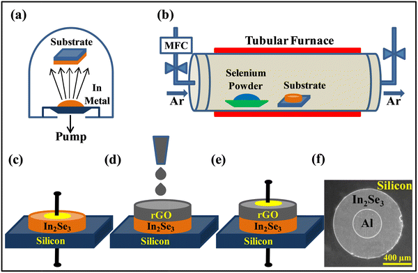 |
| | Fig. 1 The complete process step sequences for the deposition of γ-In2Se3 on the Si substrate followed by the fabrication of the rGO/γ-In2Se3/Si heterostructure-based photodetector, (a) deposition of indium metal on the Si substrate using a thermal evaporation system, (b) selenisation of the indium metal using a tubular furnace, (c) fabrication of the γ-In2Se3/Si heterostructure-based photodetector, (d) decoration of the γ-In2Se3/Si heterostructure with rGO using the drop-casting technique, € fabrication of the rGO/γ-In2Se3/Si heterostructure-based photodetector, and (f) an optical image of the fabricated γ-In2Se3/Si heterostructure-based photodetector. | |
To fabricate the rGO/In2S3/Si heterostructure, rGO was drop-cast on the In2S3/Si heterostructure. Here, rGO was synthesized using the modified Hummers’ method.29 The photodetection measurements of the In2Se3/Si and rGO/In2Se3/Si heterostructures were carried out by taking one contact from the top of the In2Se3 (or rGO) layer and another from the bottom of the Si substrate, as shown in Fig. 1(c) and (e), respectively. A circle of aluminium metal of diameter 400 μm on the In2Se3 (or rGO) layer was used as the top electrode. Fig. 1(f) shows an optical image of the fabricated γ-In2Se3/Si heterostructure-based photodetector. Here, the effective area of the device is around 0.659 mm2 (excluding the area of the metal electrode). Oriel's QEPVSI system equipped with a 300 W Xenon bulb was used for the photodetection measurements of the heterostructure. The light intensity of the system was varied by changing the width of the entrance slit. The structural characterizations of the In2Se3/Si and rGO/In2Se3/Si heterostructures were carried out using X-ray diffraction (XRD) and Raman spectroscopy. The surface morphology and composition of the In2Se3 thin film were determined using field emission scanning electron microscopy (FESEM) and energy dispersive X-ray spectroscopy (EDS), respectively. A Hitachi (U-2900) absorption spectrophotometer was used to estimate the optical band gap of the γ-In2Se3 film. Room temperature Hall measurement was carried out to determine the carrier concentration of the In2Se3 thin film and Si substrate using an Ecopia HMS 5000 system.
III. Results and discussion
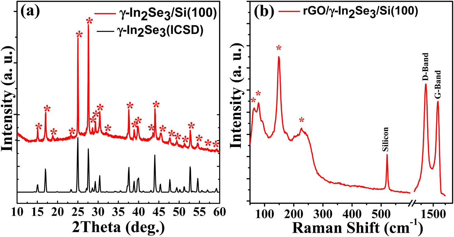
Fig. 2(a) shows the XRD pattern of the as-deposited In2Se3 thin film on the Si (100) substrate. All diffraction peaks as marked with an asterisk are consistent with the ICSD standard card of the γ-crystalline phase of In2Se3, confirming the deposition of the γ-phase of In2Se3 thin film. To further examine the γ-phase of In2Se3, micro-Raman spectroscopy has been carried out on the rGO/In2Se3/Si heterostructure. As displayed in Fig. 2(b), Raman spectroscopy shows the clear characteristics peaks (as denoted with an asterisk) associated with the different vibrational modes of γ-In2Se3. The peak at 520 cm−1 is associated with the E2 (high) mode of the Si substrate. In addition, the Raman spectrum shows two peaks at around ∼1346.4 and ∼1591.9 cm−1, which are assigned to the D- and G-band of rGO, respectively.30,31
 |
| | Fig. 2 (a) XRD of the γ-In2Se3/Si heterostructure and (b) room-temperature μ-Raman spectroscopy of the rGO/γ-In2Se3/Si heterostructure. | |
Fig. 3(a) shows the optical absorption spectra of the as-deposited γ-In2Se3 thin films with and without rGO coating on a soda-lime glass (SLG) substrate. Here, the SLG substrate was used in order to avoid the optical absorption on the Si substrate. The deposition of the γ-In2Se3 thin film on the SLG substrate was carried out usingthe same techniques as used for γ-In2Se3 on the Si substrate. With the rGO coating on the γ-In2Se3 thin film, the optical absorption is increased considerably in the wavelength range of 400–1100 nm as compared to without the rGO coating. A plot of hν vs. (αhν)2, as shown in Fig. 3(b), yields a direct bandgap of 1.81 eV, which is very close to the reported value of γ-In2Se3.19–21Fig. 4(a) shows the FESEM image of γ-In2Se3 on the Si substrate, which shows the presence of uniform nanoscale particulates on the surface of the film. In order to measure the thickness of the γ-In2Se3 thin film, cross-sectional SEM was carried out, as shown in the inset of Fig. 4(a). The thickness of γ-In2Se3 was found to be around 320 nm. Fig. 4(b) shows EDS of γ-In2Se3 on the Si substrate, which shows the presence of In and Se without any impurities. The average ratio of In to Se is approximately 2:3, indicating that the γ-In2Se3 film is stoichiometric.
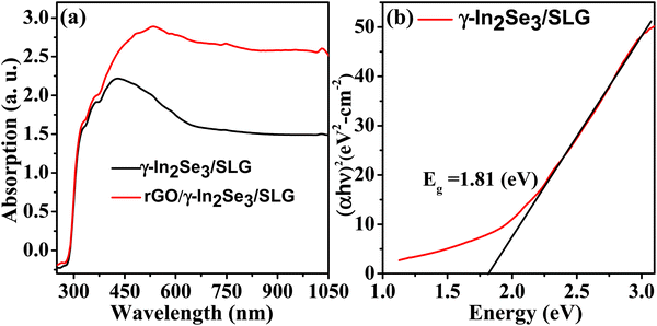 |
| | Fig. 3 (a) The optical absorption spectra of γ-In2Se3 and rGO/γ-In2Se3 thin films on the SLG substrate and (b) a plot of hν vs. (αhν)2 of the γ-In2Se3 thin film on the SLG substrate. | |
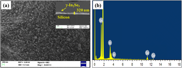 |
| | Fig. 4 (a) FESEM image of the γ-In2Se3 thin film on the Si substrate. The inset shows the cross-sectional SEM image of the γ-In2Se3/Si heterostructure and (b) EDS of the γ-In2Se3 thin film deposited on the Si substrate. | |
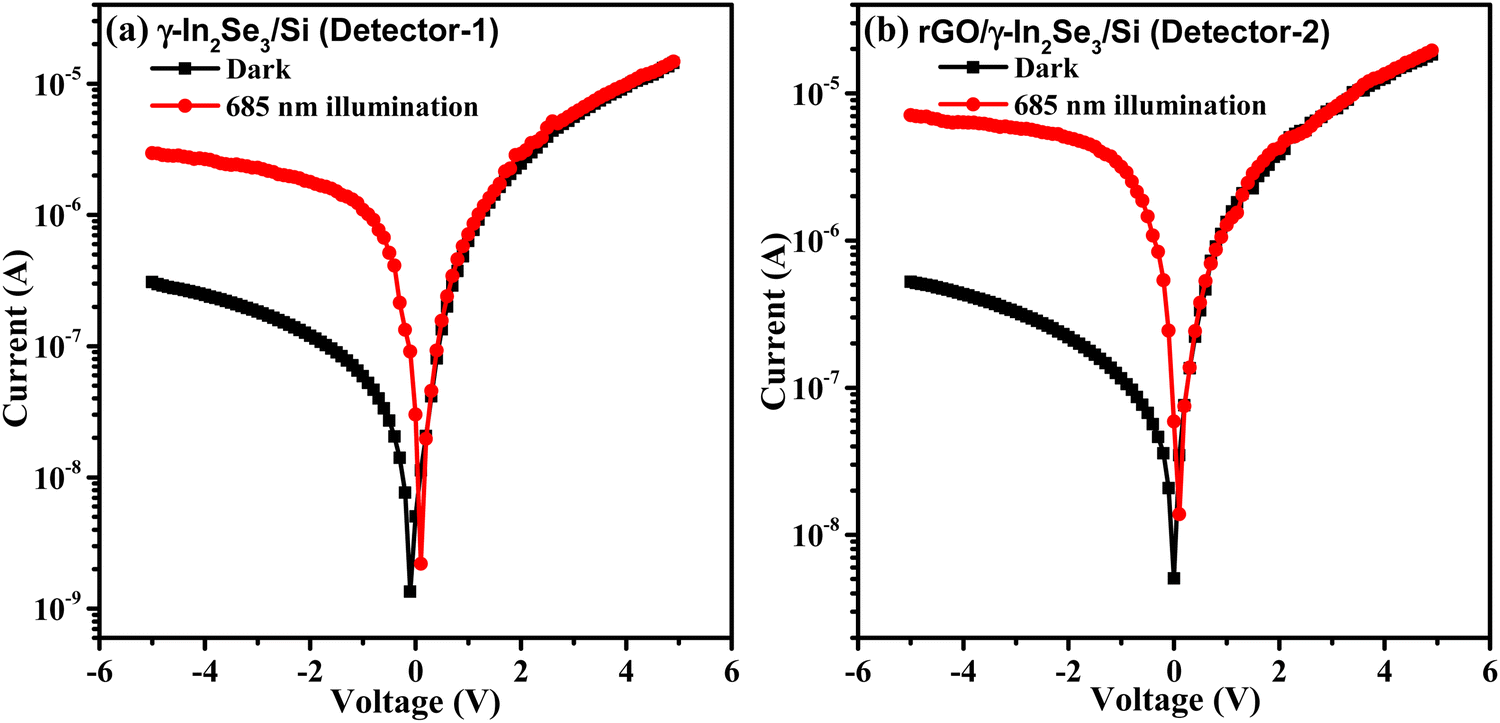
Fig. 5(a) and (b) show the I–V characteristics of the γ-In2Se3/Si (detector-1) and rGO/γ-In2Se3/Si (detector-2) heterostructures, respectively, in the dark and under the illumination of 685 nm light with a power density of 0.1 mW cm−2. Here, both heterostructures exhibit rectifying I–V characteristics which demonstrate a well-defined photodiode. Under dark conditions, the rectification ratio (on/off ratio) of detector-1 and detector-2 is 30.5 and 24.1, respectively, at an applied bias of ±3 V. Under the illumination of 685 nm, the detectors show an enhanced reverse bias current with insignificant detection under forward bias conditions. The dark current (Idark) of detector-1 and -2 is approximately 1.83 × 10⁻⁷ and 3.26 × 10⁻⁷ A, respectively, at an applied bias of −3 V. On the other hand, the current under an illumination (Iillu) of 685 nm is 2.29 × 10⁻⁶ and 5.81 × 10⁻⁶ A, resulting in a photocurrent (Iph = Iillu − Idark) of 2.10 × 10⁻⁶ and 5.48 × 10⁻⁶ A for detector-1 and detector-2, respectively. Thus, the decoration of the In2Se2/Si heterostructure with rGO improved the photocurrent of the detectors, which could be due to the increase in optical absorption of the incident light.
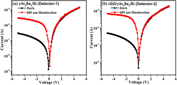 |
| | Fig. 5 Room temperature I–V characteristics of (a) γ-In2Se3/Si (detector-1) and (b) rGO/γ-In2Se3/Si (detector-2) heterostructure-based photodetectors in the dark and under an illumination of 685 nm with a power density of 0.1 mW cm−2. | |
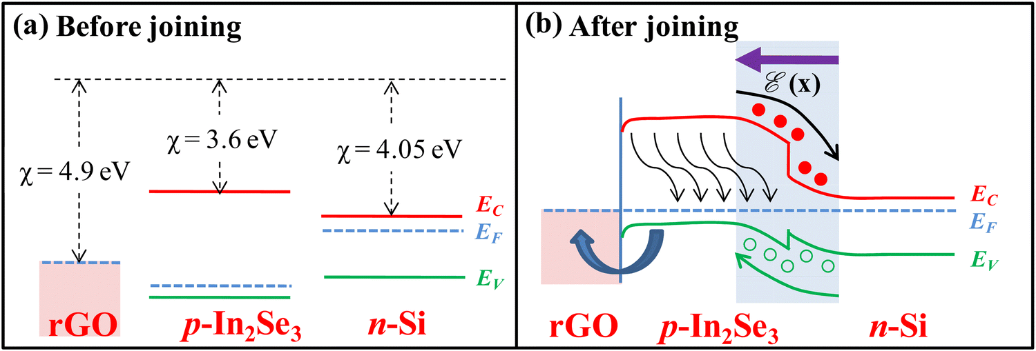
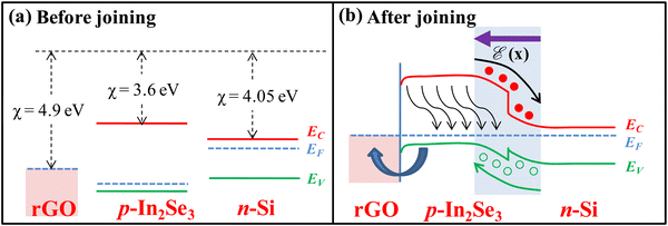
The improved photocurrent in the rGO decorated In2Se3/Si heterostructure is explained using a band diagram of the rGO/In2Se3/Si heterostructure. Fig. 6(a) shows the energy band diagram of rGO, In2Se3 and Si before joining them together. Here, the electron affinity (χ) of rGO, γ-In2Se3 and Si is taken as 4.9,32 3.633–35 and 4.05 eV,6,36 respectively, based on the previous reports. The band gap of Si is taken as 1.12,36 whereas the bandgap of γ-In2Se3 is 1.81 eV as estimated using absorption spectroscopy as shown in Fig. 3(b). The doping concentration of Si and γ-In2Se3 is estimated using Hall measurement and is found to be ∼7.5 × 1014 cm−3 for Si with n-type behavior and ∼2.28 × 1016 cm−3 for γ-In2Se3 with p-type behavior. Fig. 6(b) shows an equivalent band diagram of the heterostructure after joining individual layers together. A depletion region is created at the interface of the γ-In2Se3 and Si heterostructure, leading to the generation of a built-in electric field at the γ-In2Se3/Si interface with the direction from Si to γ-In2Se3. In addition, the In2Se3/Si heterostructure produces a type-I band alignment37 at the interface with conduction and valence band offsets of 0.45 and 0.24 eV, respectively. Under reversed bias conditions, when the heterostructure is illuminated by light, the photo-generated electron–hole pairs in the depletion region are effectively separated in opposite directions due to the presence of a high built-in electric field across the γ-In2Se3/Si interface. Here, the photo-generated electrons are swept towards the Si side and at the same time the holes are swept towards the γ-In2Se3 layer and subsequently the holes are extracted by the top rGO layer, giving rise to high photocurrent in the heterostructure. Here, rGO acts as an efficient hole transporting layer, where the recombination probability of the photo-generated charge carriers reduced drastically. Hence, the photocurrent increases significantly in the rGO decorated γ-In2Se2/Si heterostructures.
 |
| | Fig. 6 (a) The energy band diagram of rGO, p-In2Se3 and n-Si before joining, and (b) an equivalent band diagram of the rGO/p-In2Se3/n-Si heterostructure. | |
The figures-of-merit like responsivity, detectivity and sensitivity are calculated to evaluate the performance of the detectors. The responsivity (Rλ) of the photodetectors, as defined by the ratio of the photocurrent to the intensity of the illuminated light, is calculated by using the relation,6,38–40Rλ = Iλ/PλS, where Iλ is the photocurrent (Iillumination − Idark), Pλ is the light intensity and S is the effective area of the heterostructure. Fig. 7(a) shows the voltage dependent responsivity of detector-1 and detector-2 under an illumination of 685 nm. The responsivity of the detectors increases with applied reverse bias voltage, which is due to the increase in photocurrent. At higher applied reverse bias voltage, the photo-generated charge carriers are effectively separated due to the presence of the high internal electric field at the In2Se3/Si interface, which resulted in high photocurrent. Moreover, the responsivity of detector-2 is significantly higher than that of detector-1 because of the top rGO layer, which further reduces the recombination of the photo-generated charge carriers due to its efficient hole transporting properties. The values of Rλ were found to be 4.6 and 9.5 A W−1 for detector-1 and detector-2, respectively, under the illumination of 685 nm at an applied bias of −3 V. Fig. 7(b) shows the spectral response of the detectors in the wavelength range of 300–1300 nm, measured at an applied bias of −3 V with light intensity of 0.1 mW cm−2. The detectors showed a peak detection at around λ = 685 and 900 nm, corresponding to the optical absorption edge of In2Se3 and Si, respectively. The values of Rλ for detector-1 and detector-2 were ∼9 and 27 A W−1, respectively, under the illumination of 900 nm at an applied bias of −3 V. In addition, the detectivity (D*) of the photodetectors is estimated using the relation,38,41D* = Rλ/(2eJd)1/2, where Rλ is the responsivity of the photodetectors and Jd is the dark current density. Fig. 7(c) shows the voltage dependent detectivity of detector-1 and detector-2 under the illumination of 685 nm, which shows a maximum detectivity at an applied bias of −1.5 V. The D* values of detector-1 and detector-2 were found to be ∼1.18 × 10¹² and ∼2.55 × 1012 cm Hz1/2 W−1, respectively, at an applied bias of −1.5 V. Moreover, the sensitivity of the detectors, as defined by the ratio of photocurrent to the dark current, is calculated using the relation,39,41 Sensitivity = Iph/Idark, where Iph and Idark are the photocurrent and dark current of the detector, respectively. The voltage dependent sensitivity of the detectors is shown in Fig. 7(d), which shows a maximum sensitivity at an applied bias of −1 V. The sensitivities of the detectors were found to be 17.5 and 26.3 for detector-1 and detector-2 at an applied bias of −1 V, respectively.
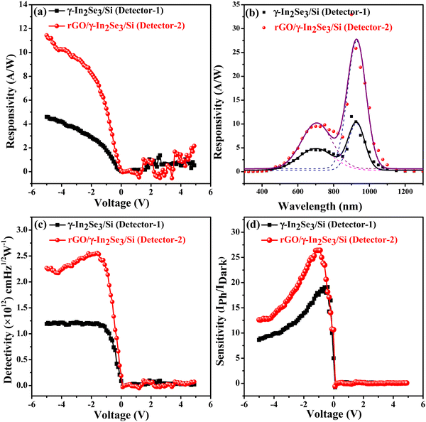 |
| | Fig. 7 (a) The voltage dependent photo-responsivity of the detectors under an illumination of 685 nm, (b) the spectral response of the detectors in the wavelength range of 300–1300 nm, measured at an applied bias of −3 V with light intensity of 0.1 mW cm−2, (c) the voltage dependent specific detectivity of the detectors under an illumination of 685 nm, and (d) the voltage dependent sensitivity of the detectors under an illumination of 685 nm. | |
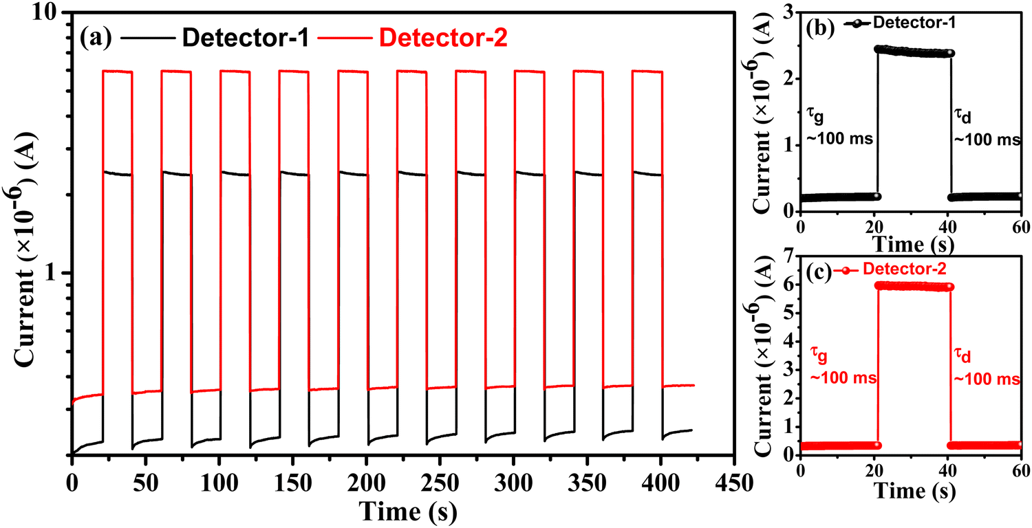
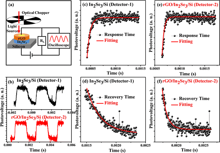
In order to further investigate the photo-response characteristics of the detectors, the temporal response of the devices has been investigated. Fig. 8(a) depicts the temporal response of the detectors under the illumination of 685 nm at an applied bias of −3 V. The temporal response remains identical after several cycles, confirming the excellent stability of the photodetectors. At the onset of illumination of 685 nm, the current increases and saturates within the response time. After the illumination is tuned off, the current returns to its initial value within the recovery time. Here, the response and recovery times of the detectors were found to be ∼100 ms, which is not accurate as the time interval between two data points is ∼100 ms.
 |
| | Fig. 8 (a) The temporal response of the detectors under the illumination of 685 nm at an applied bias of −3 V on semi-log scale, (b) zoomed-in view of one ON/OFF cycle of detector-1, and (c) zoomed-in view of one ON/OFF cycle of detector-2. | |
In order to estimate the precise response and recovery times, we have used an ultrafast time measurement setup, which is shown in Fig. 9(a). The transient response of the detectors using an ultrafast time measurement under a pulsed light source of 685 nm with a frequency of 500 Hz is shown in Fig. 9(b). The time constants of the detectors were estimated by fitting the transient response with the following equations,41,42
| | | V(t) = Vdark + A{1 − exp[(t0 − t)/τg]} | (1) |
and
| | | V(t) = Vdark + A{1 − exp[(t0 − t)/τd]} | (2) |
where
Vdark is the dark photo-voltage,
A is the scaling constant,
t0 is the time when the illumination was switched ON or OFF and
τg/
τd are the response/recovery times, respectively. The fitting of the transient responses with
eqn (1) and (2) for detector-1 and detector-2 is shown in
Fig. 9(c)–(f). In detector-1 and -2, the response/recovery times were 60/230 μs and 40/90 μs, respectively. In the present case, the fast temporal response in detector-2 could be due to the efficient hole transporting properties of the top rGO layer and the presence of a high internal electric field at the In
2Se
3/Si interface. In
Table 1, we have summarized the key figures-of-merit of our device and compared it with the various 2D-layered/Si heterostructure-based photodetectors reported in the literature, considering the significance of large area deposition of 2D materials for large scale production.
 |
| | Fig. 9 (a) An ultrafast time measurement setup, (b) the transient response of the detectors under a pulsed light source of 685 nm with a frequency of 500 Hz, and (c)–(f) the response and recovery of detector-1 and detector-1 under a pulsed light source of 685 nm with a frequency of 500 Hz. | |
Table 1 Comparison of figures-of-merit of our device with the various 2D-layered heterostructure-based photodetectors reported in the literature, considering the significance of large area deposition of 2D materials for large scale production
| Photodetector |
Bias voltage (V) |
λ (nm) |
R
λ
(A W−1) |
D* (Jones) |
τ
g/τd (ms) |
| γ-In2Se3/n-Si17 |
0 |
808 |
0.57 |
2.6 × 10¹² |
0.035/0.115 |
| Graphene/In2Se328 |
0.35 |
1550 |
1.17 |
— |
1.76/1.86 |
| In2S3/CIGS43 |
−1 |
870 |
2.06 |
2.3 × 10¹¹ |
— |
| n-In2S3/p-Si44 |
2 |
750 |
0.68 |
2.5 × 10¹¹ |
— |
| MoS2/p-Si45 |
0 |
532 |
0.253 |
1 × 10⁹ |
85/136 |
| n-MoS2/n-Si46 |
−2 |
650 |
11.9 |
2.1 × 10¹⁰ |
0.030/0.071 |
| MoS2 Schottky MSM47 |
10 |
532 |
0.57 |
1 × 10¹⁰ |
0.07/0.11 |
| MoS2 Schottky MSM48 |
3 |
532 |
0.55 |
— |
0.2/1.7 |
| WS2/Si49 |
0 |
980 |
0.224 |
1.5 × 10¹² |
0.016/0.029 |
| rGO/In2Se3/Si |
−3 |
λ = 685 |
R
λ
= 9.5 |
2.39 × 10¹² |
0.04/0.09 |
| (This work) |
λ = 900 |
R
λ
= 27 |
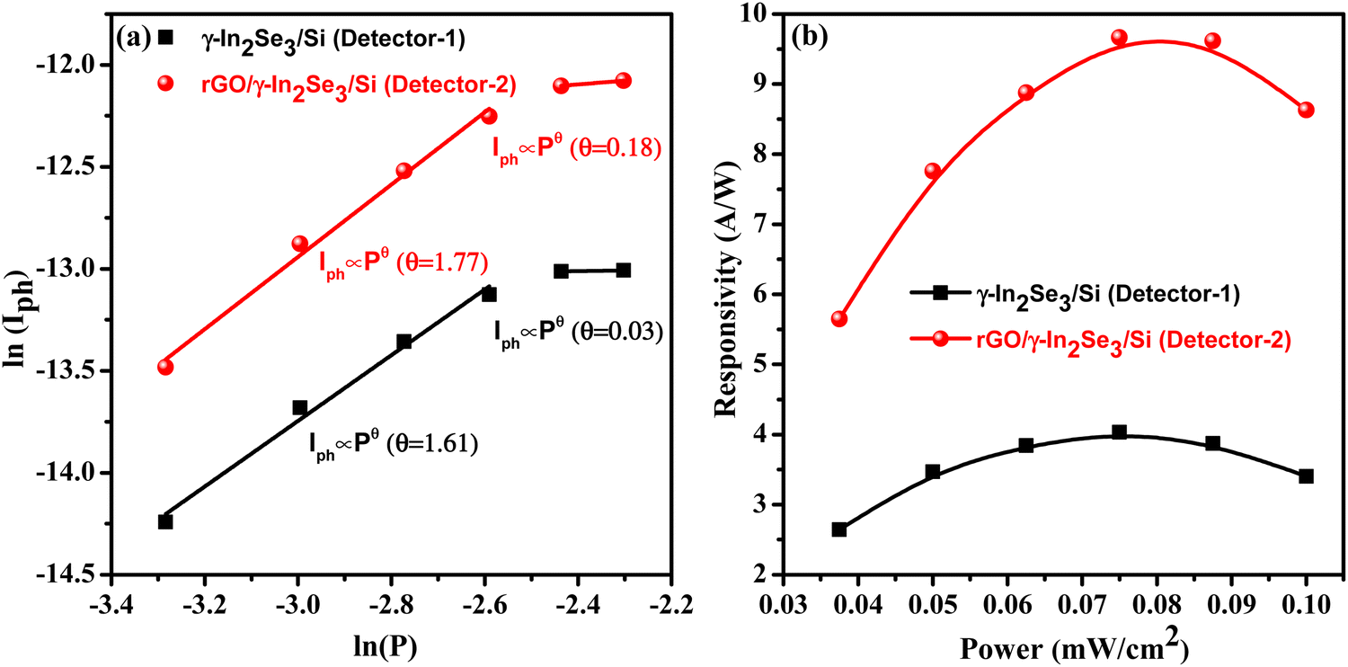
The variation of the photocurrent with illuminated light intensity at an applied bias of −3 V is shown in Fig. 10(a). The photocurrent of the detectors increases with increasing light intensity with a power law,50IPh ∝ Pθ, where Iph is the photocurrent of the detectors and θ is an exponent which determines the conduction process of the photo-generated charge carriers. In Fig. 10(a), we observed two linear regions (region-I and region-II). In region-I (where, the power density of the illuminated light is low), the values of θ are 1.61 and 1.77 for detector-1 and detector-2, respectively. The high value of θ (greater than unity) in region-I suggests the effective separation of photogenerated charge carriers across the depletion region,51 which resulted in an enhance photocurrent and thereby the responsivity of the detector is increased as illustrated in Fig. 10(b). In region-II (where, the power density of the illuminated light is high), the values of θ are 0.03 and 0.18 for detector-1 and detector-2, respectively. Here, the non-unity value of θ in region-II suggests a complex recombination or scattering of the photogenerated charge carriers due to more population density of the photogenerated charge carriers,52,53 which resulted in a decrease in the responsivity of the detectors, as shown in Fig. 10(b).
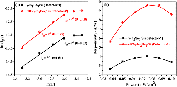 |
| | Fig. 10 (a) The variation of the photocurrent of the detectors with illuminated light intensity at an applied bias of −3 V and (b) the variation of the photo-responsivity of the detectors with illuminated light intensity at an applied bias of −3 V. | |
IV. Conclusion
In conclusion, we have demonstrated a high performance rGO decorated γ-In2Se3/Si heterostructure-based broadband photodetector ranging from 400–1200 nm. The rGO/γ-In2Se3/Si heterostructure showed an enhanced photo-responsivity of ∼9.5 and ∼27 A W−1 under the illumination of 685 and 900 nm, respectively, at an applied bias of −3 V. In addition, the heterostructure showed high sensitivity with fast response/recovery times (40/90 μs). The enhanced figures-of-merit of the rGO/γ-In2Se3/Si heterostructure are due to the increase in optical absorption of incident light and efficient hole transporting properties of the top rGO layer, which effectively reduces the recombination of the photogenerated charge carriers.
Author contributions
Prof. S. B. Krupanidhi, Prof. K. K. Nanda, Dr Sujit Das and Dr Basanta Roul generated the idea and designed experiments. Dr Basanta Roul and A. M. C. performed experiments. Dr Basanta Roul, M. K., and K. L. K., prepared the manuscript. All authors participated in the discussion of the experimental results and revision of the manuscript.
Conflicts of interest
The authors declare no conflicts of interest.
References
- T. Tan, X. Jiang, C. Wang, B. Yao and H. Zhang, 2D Material Optoelectronics for Information Functional Device Applications: Status and Challenges, Adv. Sci., 2020, 7(11), 2000058 CrossRef CAS PubMed.
- J. Cheng, C. Wang, X. Zou and L. Liao, Recent Advances in Optoelectronic Devices Based on 2D Materials and Their Heterostructures. Adv, Opt. Mater., 2019, 7(1), 1–15 Search PubMed.
- J. An, X. Zhao, Y. Zhang, M. Liu, J. Yuan, X. Sun, Z. Zhang, B. Wang, S. Li and D. Li, Perspectives of 2D Materials for Optoelectronic Integration, Adv. Funct. Mater., 2022, 32(14), 1–24 Search PubMed.
- S. Kang, D. Lee, J. Kim, A. Capasso, H. S. Kang, J. W. Park, C. H. Lee and G. H. Lee, 2D Semiconducting Materials for Electronic and Optoelectronic Applications: Potential and Challenge, 2D Mater., 2020, 7(2), 022003 CrossRef CAS.
- D. K. Singh, R. Pant, B. Roul, A. M. Chowdhury, K. K. Nanda and S. B. Krupanidhi, Temperature-Dependent Electrical Transport and Optoelectronic Properties of SnS2/p-Si Heterojunction, ACS Appl. Electron. Mater., 2020, 2(7), 2155–2163 CrossRef CAS.
- B. Roul, R. Pant, A. M. Chowdhury, G. Chandan, D. K. Singh, S. Chirakkara, K. K. Nanda and S. B. Krupanidhi, Highly Responsive ZnO/AlN/Si Heterostructure-Based Infrared- and Visible-Blind Ultraviolet Photodetectors with High Rejection Ratio, IEEE Trans. Electron Devices, 2019, 66(3), 1345–1352 CAS.
- D. Wu, J. Guo, C. Wang, X. Ren, Y. Chen, P. Lin, L. Zeng, Z. Shi, X. J. Li and C. X. Shan,
et al., Ultrabroadband and High-Detectivity Photodetector Based on WS2/Ge Heterojunction through Defect Engineering and Interface Passivation, ACS Nano, 2021, 15(6), 10119–10129 CrossRef PubMed.
- L. Zeng, D. Wu, J. Jie, X. Ren, X. Hu, S. P. Lau, Y. Chai and Y. H. Tsang, van der Waals Epitaxial Growth of Mosaic-Like 2D Platinum Ditelluride Layers for Room-Temperature Mid-Infrared Photodetection up to 10.6 Mm, Adv. Mater., 2020, 32(52), 1–11 Search PubMed.
- D. Wu, J. Guo, J. Du, C. Xia, L. Zeng, Y. Tian, Z. Shi, Y. Tian, X. J. Li and Y. H. Tsang,
et al., Highly Polarization-Sensitive, Broadband, Self-Powered Photodetector Based on Graphene/PdSe2/Germanium Heterojunction, ACS Nano, 2019, 13(9), 9907–9917 CrossRef CAS PubMed.
- D. Wu, C. Jia, F. Shi, L. Zeng, P. Lin, L. Dong, Z. Shi, Y. Tian, X. Li and J. Jie, Mixed-Dimensional PdSe2/SiNWA Heterostructure Based Photovoltaic Detectors for Self-Driven, Broadband Photodetection, Infrared Imaging and Humidity Sensing, J. Mater. Chem. A, 2020, 8(7), 3632–3642 RSC.
- D. Wu, C. Guo, Z. Wang, X. Ren, Y. Tian, Z. Shi, P. Lin, Y. Tian, Y. Chen and X. Li, A Defect-Induced Broadband Photodetector Based on WS2/Pyramid Si 2D/3D Mixed-Dimensional Heterojunction with a Light Confinement Effect, Nanoscale, 2021, 13(31), 13550–13557 RSC.
- J. F. Sánchez-Royo, A. Segura, O. Lang, E. Schaar, C. Pettenkofer, W. Jaegermann, R. Roa and A. Chevy, Optical and Photovoltaic Properties of Indium Selenide Thin Films Prepared by van der Waals Epitaxy, J. Appl. Phys., 2001, 90(6), 2818–2823 CrossRef.
- H. Bouzouita, N. Bouguila, S. Duchemin, S. Fiechter and A. Dhouib, Preparation and Characterization of In2Se3 Thin Films. Renew, Energy, 2002, 25(1), 131–138 CAS.
- M. S. Claro, J. Grzonka, N. Nicoara, P. J. Ferreira and S. Sadewasser, Wafer-Scale Fabrication of 2D β-In2Se3 Photodetectors. Adv, Opt. Mater., 2021, 9(1), 1–9 Search PubMed.
- N. Balakrishnan, E. D. Steer, E. F. Smith, Z. R. Kudrynskyi, Z. D. Kovalyuk, L. Eaves, A. Patanè and P. H. Beton, Epitaxial Growth of γ-InSe and α, β, and γ-In2Se3 on ε-GaSe, 2D Mater., 2018, 5(111), 035026 CrossRef.
- X. Sun, B. Yu, G. Ng, T. D. Nguyen and M. Meyyappan, III-VI Compound Semiconductor Indium Selenide (In2Se3) Nanowires: Synthesis and Characterization, Appl. Phys. Lett., 2006, 89(23), 1–4 Search PubMed.
- C. Y. Wu, J. W. Kang, B. Wang, H. N. Zhu, Z. J. Li, S. R. Chen, L. Wang, W. H. Yang, C. Xie and L. B. Luo, Defect-Induced Broadband Photodetection of Layered γ-In2Se3 Nanofilm and Its Application in near Infrared Image Sensors, J. Mater. Chem. C, 2019, 7(37), 11532–11539 RSC.
- A. Pfitzner and H. D. Lutz, Redetermination of the Crystal Structure of γ-In2Se3 by Twin Crystal X-Ray Method, J. Solid State Chem., 1996, 124(2), 305–308 CrossRef CAS.
- C. Julien, A. Chlwy and D. Siapkas, Optical Properties of In2Se3 Phases, Phys. Stat. Sol. (a), 1990, 118, 553–559 CrossRef CAS.
- S. Marsillac, A. M. Combot Marie, J. C. Bernede and A. Conan, Experimental Evidence of the Low-Temperature Formation of γ-In2Se3, Thin Films, 1996, 288 Search PubMed.
- C. H. De Groot and J. S. Moodera, Growth and Characterization of a Novel In2Se3 Structure, J. Appl. Phys., 2001, 89(8), 4336–4340 CrossRef CAS.
- S. K. Chakraborty, B. Kundu, B. Nayak, S. P. Dash and P. K. Sahoo, Challenges and Opportunities in 2D Heterostructures for Electronic and Optoelectronic Devices, iScience, 2022, 25(3), 103942 CrossRef CAS PubMed.
- R. B. Jacobs-gedrim, M. Shanmugam, N. Jain and C. A. Durcan, Supporting Information Extraordinary Photoresponse in Two-Dimensional In2Se3 Nanosheets, ACS Nano, 2014, 8(1), 514–521 CrossRef CAS PubMed.
- Q. L. Li, Y. Li, J. Gao, S. D. Wang and X. H. Sun, High Performance Single In2Se3 Nanowire Photodetector, Appl. Phys. Lett., 2011, 99(24), 1–4 Search PubMed.
- T. Zhai, X. Fang, M. Liao, X. Xu, L. Li, B. Liu, Y. Koide, Y. Ma, J. Yao, Y. Bando and D. Golberg, Fabrication of High-Quality In2Se3 Nanowire Arrays toward High-Performance Visible-Light Photodetectors, ACS Nano, 2010, 4(3), 1596–1602 CrossRef CAS PubMed.
- S. Chen, X. Liu, X. Qiao, X. Wan, K. Shehzad, X. Zhang, Y. Xu and X. Fan, Facile Synthesis of γ-In2Se3 Nanoflowers toward High Performance Self-Powered Broadband γ-In2Se3/Si Heterojunction Photodiode, Small, 2017, 13(18), 1–7 Search PubMed.
- R. K. Mech, S. V. Solanke, N. Mohta, M. Rangarajan and D. N. Nath, In2Se3 Visible/Near-IR Photodetector with Observation of Band-Edge in Spectral Response, IEEE Photonics Technol. Lett., 2019, 31(11), 905–908 CAS.
- W. Shao, X. Xie, Y. Zheng, W. Wang, T. Li, F. Wang, Y. Wang, S. Law and T. Gu, Near-Infrared Photodetection in Graphene/β-In2Se3 Heterostructure, Asia Commun. Photonics Conf., 2020, 10–12 Search PubMed.
- W. S. Hummers and R. E. Offeman, Preparation of Graphitic Oxide, J. Am. Chem. Soc., 1958, 80(6), 1339 CrossRef CAS.
- M. A. Khan, K. L. Kumawat, K. K. Nanda and S. B. Krupanidhi, Reduced Graphene Oxide-Based Broad Band Photodetector and Temperature Sensor: Effect of Gas Adsorption on Optoelectrical Properties, J. Nanopart. Res., 2018, 20, 11 CrossRef.
- K. L. Kumawat, D. K. Singh, K. K. Nanda and S. B. Krupanidhi, Solution-Processed SnSe2-RGO-Based Bulk Heterojunction for Self-Powered and Broadband Photodetection, ACS Appl. Electron. Mater., 2021, 3(7), 3131–3138 CrossRef CAS.
- V. S. Bhati, D. Sheela, B. Roul and R. Raliya, NO2 Gas Sensing Performance Enhancement Based on Reduced NO2 Gas Sensing Performance Enhancement Based on Reduced Graphene Oxide Decorated V2O5, Nanotechnology, 2019, 30, 224001 CrossRef CAS PubMed.
- S. I. Drapak, Z. D. Kovalyuk, V. V. Netyaga and V. B. Orletskii, On the Mechanisms of Current Transfer in N-In2Se3-p-GaSe Heterostructures, Tech. Phys. Lett., 2002, 28(9), 707–710 CrossRef CAS.
- J. M. Pastor, A. Segura, J. L. Valdes and A. Chevy, Electrical and Photovoltaic Properties of Indium-Tin-Oxide/p-InSe/Au Solar Cells, J. Appl. Phys., 1987, 62(4), 1477–1483 CrossRef.
- S. M. Poh, S. J. R. Tan, H. Wang, P. Song, I. H. Abidi, X. Zhao, J. Dan, J. Chen, Z. Luo and S. J. Pennycook,
et al., Molecular-Beam Epitaxy of Two-Dimensional In2Se3 and Its Giant Electroresistance Switching in Ferroresistive Memory Junction, Nano Lett., 2018, 18(10), 6340–6346 CrossRef CAS PubMed.
- D. Song and B. Guo, Electrical Properties and Carrier Transport Mechanisms of N-ZnO/SiOx/n-Si Isotype Heterojunctions with Native or Thermal Oxide Interlayers, J. Phys. D: Appl. Phys., 2009, 42, 025103 CrossRef.
- B. Roul, M. Kumar, M. K. Rajpalke, T. N. Bhat and S. B. Krupanidhi, Binary Group III-Nitride Based Heterostructures: Band Offsets and Transport Properties, J. Phys. D: Appl. Phys., 2015, 48(42), 423001 CrossRef.
- B. Roul, R. Pant, S. Chirakkara, G. Chandan, K. K. Nanda and S. B. Krupanidhi, Enhanced UV Photodetector Response Of, IEEE Trans. Electron Devices, 2017, 64(10), 4161–4166 CAS.
- R. K. Pant, D. K. Singh, B. Roul, A. M. Chowdhury, G. Chandan, K. K. Nanda and S. B. Krupanidhi, Photodetection Properties of Nonpolar A-Plane GaN Grown by Three Approaches Using Plasma-Assisted Molecular Beam Epitaxy, Phys. Status Solidi A, 2019, 216(18), 1–7 CrossRef.
- R. Pant, A. Shetty, G. Chandan, B. Roul, K. K. Nanda and S. B. Krupanidhi, In-Plane Anisotropic Photoconduction in Nonpolar Epitaxial a-Plane GaN, ACS Appl. Mater. Interfaces, 2018, 10(19), 16918–16923 CrossRef CAS PubMed.
- D. K. Singh, R. Pant, A. M. Chowdhury, B. Roul, K. K. Nanda and S. B. Krupanidhi, Defect-Mediated Transport in Self-Powered, Broadband, and Ultrafast Photoresponse of a MoS2/AlN/Si-Based Photodetector, ACS Appl. Electron. Mater., 2020, 2(4), 944–953 CrossRef CAS.
- B. Roul, D. K. Singh, A. M. Chowdhury, M. Kumari, K. L. Kumawat, K. K. Nanda and S. B. Krupanidhi, Enhancement of Photoresponsivity of β-In2S3/Si Broadband Photodetector by Decorating With Reduced-Graphene Oxide, IEEE Trans. Electron Devices, 2022, 69(8), 4355–4361 CAS.
- X. Zeng, J. Lontchi, M. Zhukova, L. Fourdrinier, I. Qadir, Y. Ren, E. Niemi, G. Li and D. Flandre, High-Responsivity Broadband Photodetection of an Ultra-Thin In2S3/CIGS Heterojunction on Steel, Opt. Lett., 2021, 46(10), 2288 CrossRef PubMed.
- R. A. Ismail, N. F. Habubi and M. M. Abbod, Preparation of High-Sensitivity In2S3/Si Heterojunction Photodetector by Chemical Spray Pyrolysis. Opt, Quantum Electron., 2016, 48(10), 1–14 Search PubMed.
- X. Liu, F. Li, M. Xu, T. Shen, Z. Yang, W. Fan and J. Qi, High Response, Self-Powered Photodetector Based on the Monolayer MoS2/P–Si Heterojunction with Asymmetric Electrodes, Langmuir, 2018, 34(47), 14151–14157 CrossRef CAS PubMed.
- Y. Zhang, Y. Yu, L. Mi, H. Wang, Z. Zhu, Q. Wu, Y. Zhang and Y. Jiang,
In Situ Fabrication of Vertical Multilayered MoS2/Si Homotype Heterojunction for High-Speed Visible – Near- Infrared Photodetectors, Small, 2016, 12(8), 1062–1071 CrossRef CAS PubMed.
- D. S. Tsai, K. K. Liu, D. H. Lien, M. L. Tsai, C. F. Kang, C. A. Lin, L. J. Li and J. H. He, Few-Layer MoS2 with High Broadband Photogain and Fast Optical Switching for Use in Harsh Environments, ACS Nano, 2013, 7(5), 3905–3911 CrossRef CAS PubMed.
- J. Lu, J. H. Lu, H. Liu, B. Liu, K. X. Chan, J. Lin, W. Chen, K. P. Loh and C. H. Sow, Improved Photoelectrical Properties of MoS2 Films after Laser Micromachining, ACS Nano, 2014, 8(6), 6334–6343 CrossRef CAS PubMed.
- E. Wu, D. Wu, C. Jia, Y. Wang, H. Yuan, L. Zeng, T. Xu, Z. Shi, Y. Tian and X. Li, In Situ Fabrication of 2D WS2/Si Type-II Heterojunction for Self-Powered Broadband Photodetector with Response up to Mid-Infrared, ACS Photonics, 2019, 6(2), 565–572 CrossRef CAS.
- A. M. Chowdhury, G. Chandan, R. Pant, B. Roul, D. K. Singh, K. K. Nanda and S. B. Krupanidhi, Self-Powered, Broad Band, and Ultrafast InGaN-Based Photodetector, ACS Appl. Mater. Interfaces, 2019, 11(10), 10418–10425 CrossRef CAS PubMed.
- E. P. Mukhokosi, B. Roul, S. B. Krupanidhi and K. K. Nanda, Toward a Fast and Highly Responsive SnSe2-Based Photodiode by Exploiting the Mobility of the Counter Semiconductor, ACS Appl. Mater. Interfaces, 2019, 11, 6184–6194 CrossRef CAS PubMed.
- Z. Jia, J. Xiang, F. Wen, R. Yang, C. Hao and Z. Liu, Enhanced Photoresponse of SnSe-Nanocrystals-Decorated WS2 Monolayer Phototransistor, ACS Appl. Mater. Interfaces, 2016, 8(7), 4781–4788 CrossRef CAS PubMed.
- E. P. Mukhokosi, S. B. Krupanidhi and K. K. Nanda, Band Gap Engineering of Hexagonal SnSe2 Nanostructured Thin Films for Infra-Red Photodetection, Sci. Rep., 2017, 7(1), 1–10 CrossRef CAS PubMed.
|
| This journal is © The Royal Society of Chemistry 2023 |
Click here to see how this site uses Cookies. View our privacy policy here. 
 Open Access Article
 This Open Access Article is licensed under a Creative Commons Attribution-Non Commercial 3.0 Unported Licence
 *ab,
Arun Malla
Chowdhury
*ab,
Arun Malla
Chowdhury