
 Open Access Article
 This Open Access Article is licensed under a Creative Commons Attribution-Non Commercial 3.0 Unported Licence
Electroactive substrates for surface-enhanced Raman spectroscopy based on overgrown gold-nanoparticle arrays by electrodeposition on indium tin oxide†
Nerea
González-Pato
ab,
Xavier Rodriguez
Rodriguez
 a,
Nicola
Pellizzi
ac,
Claudia
Fasolato
d,
Judith
Guasch
abe,
Paolo
Postorino
f,
Jaume
Veciana
ab,
Alejandro R.
Goñi
*ag and
Imma
Ratera
*ab
a,
Nicola
Pellizzi
ac,
Claudia
Fasolato
d,
Judith
Guasch
abe,
Paolo
Postorino
f,
Jaume
Veciana
ab,
Alejandro R.
Goñi
*ag and
Imma
Ratera
*ab
aInstitut de Ciència de Materials de Barcelona (ICMAB-CSIC), Campus UAB, Bellaterra 08193, Spain. E-mail: iratera@icmab.es; goni@icmab.es
bCIBER de Bioingeniería, Biomateriales y Nanomedicina (CIBER-BBN), Spain
cPhysics Department, University of Calabria, Ponte P. Bucci cubo 33B, 87036 Rende (CS), Italy
dCNR-ISC, Istituto dei Sistemi Complessi, c/o Sapienza Università di Roma, P.le Aldo Moro 5, 00185 Roma, Italy
eDynamic Biomimetics for Cancer Immunotherapy, Max Planck Partner Group, ICMAB-CSIC, Campus UAB, Bellaterra, 08193 Barcelona, Spain
fDipartimento di Fisica, Università Sapienza, P.le Aldo Moro 5, 00185 Rome, Italy
gICREA, Passeig Lluís Companys 23, 08010 Barcelona, Spain
First published on 16th February 2023
Abstract
We report an easy and low-cost method for the preparation of highly homogeneous electroactive substrates that can be used simultaneously for surface-enhanced Raman spectroscopy (SERS) and electrochemical measurements. The choice of conductive indium tin oxide (ITO) as a substrate is based on its excellent electrical conductivity and transparency. However, its typically high roughness makes the subsequent metal deposition with traditional methods very challenging, making them time-consuming and costly. To circumvent this problem, we developed a simple two-step procedure consisting of first the deposition of a quasi-hexagonal pattern of homogeneously distributed gold nanoparticles (AuNPs) by block-copolymer micellar lithography on ITO. Subsequently, the AuNPs act as seeds for further gold growth by electrodeposition on the pre-patterned ITO substrate. In this way, we reproducibly achieved substrates (>50) with an average gold coverage of (40 ± 5) % and many hot spots due to a small average inter-particle distance of (15 ± 5) nm. These substrates exhibit a strong and homogeneous Raman signal, as determined using 2D maps obtained with the standard Raman tag molecule 4-mercaptobenzoic acid. Moreover, the electrochemical performance of the developed conductive SERS substrates was demonstrated using a Michael addition reaction monitored by Raman scattering. This reaction occurs between the hydroquinone/benzoquinone redox pair and a biologically relevant analyte, but only takes place in one of the redox states of the hydroquinone/benzoquinone system.
Introduction
Surface-enhanced Raman spectroscopy (SERS) is a fast, non-invasive technique with excellent molecular fingerprinting capabilities, also at room temperature, and amplifies by several orders of magnitude the vibrational Raman signals of molecules on substrates that exhibit localized surface plasmon resonances.1 In fact, SERS can boost Raman sensitivity to enable the detection of very low concentrations of analytes even down to the single-molecule level.2–4 For these reasons, SERS is increasingly used in many different fields for a wide variety of applications, such as materials science, biology, diagnostics, biomedicine, forensic science, etc.5 A significant enhancement of the Raman signal requires the presence of certain regions, called hot spots, which correspond to small gaps between metal nanoparticles or nanoscale surface protrusions. It is at these gaps or protrusions where the electromagnetic field becomes strongly enhanced by the lightning-rod effect, amplifying the Raman signal of the molecules close to such motifs. The most used metals for SERS are Ag and Au partly because, by proper nanostructuring, they can exhibit localized surface plasmon resonances in the whole spectral range from visible to infrared wavelengths.4 There are many reported procedures to create small gaps between metallic particles in the range of nanometers. The current methods are either too fabrication-intensive or lack reproducibility from one substrate to another and/or display insufficient homogeneity across the substrate. One of the most attractive surface shapes for SERS substrates is particles with flower-like motifs, mainly obtained by electrochemistry, because they are rough and full of hot spots. However, with few exceptions,6 these substrates are difficult to reproduce because the resulting particles are randomly distributed on the surface with poor control of the shape of the flower-like motifs.7–9 Other methods involve the use of electron-beam lithography, which allows for great reproducibility and control over the hot spot formation, but it is very time-consuming and expensive, which can be an obstacle to scale up.10Although there is great interest in the preparation of efficient SERS substrates,11 novel research directions are opening up by adding a functionality to the SERS substrates if they are electroactive. Such SERS substrates are particularly suitable for in situ and/or in operando monitoring of electrochemical processes. For example, the combination of SERS and electrochemistry has been already implemented not only for the characterization of pharmaceutical compounds,12–14 carboxylates derivatives,15 peptides,15 polymeric materials16 or dyes like rhodamine,17 but also for monitoring switchable redox molecules.12,14,18 Redox molecular switches are molecules that, under an electrochemical input, show two or more discrete stable electronic states, exhibiting different chemical or/and physical properties.19–22 These molecules show great potential to be used as logic gates in molecular electronics.19,23,24 In this context, further development of reproducible, easy-to-fabricate, electroactive SERS substrates would certainly deepen our understanding of molecular switching processes, contributing to improve the performance of future molecule-based electronic devices.
The use of a conductive substrate has an additional advantage. It allows performing the subsequent electrodeposition steps, with the purpose of achieving precise control over the average inter-particle distance, i.e. the gaps between metal protrusions, for the realization of hot spots. One approach that fulfills these characteristics is the electrodeposition of metallic nanoparticles on a conductive substrate, such as indium tin oxide (ITO).24–26 However, due to its roughness, it is challenging with the existing strategies to achieve a homogeneous distribution of gaps and satisfying reproducibility.27
In this work, we provide a possible solution by demonstrating the reproducible preparation of conductive and transparent ITO substrates suitable for simultaneous SERS and electrochemical measurements. For this purpose, we have developed a simple two-step procedure which, in the first step, involves the deposition of gold nanoparticles (AuNPs) on ITO by using block-copolymer micellar lithography (BCML) and plasma etching.28–36 The so-formed quasi-hexagonal pattern of AuNPs acts as seeds for further electrodeposition of gold on top of the pre-patterned AuNPs, taking advantage of the conductivity of the ITO substrate. Thus, by controlling the AuNP overgrowth times, we achieved smaller inter-particle distances typically of (15 ± 5) nm, generating a surface with a collection of hot spots. Substrates exhibit a strong and homogeneous Raman signal, as determined by 2D maps performed with the standard Raman tag molecule 4-mercaptobenzoic acid. More importantly, we demonstrate the suitability of the developed conductive SERS substrates for electrochemical applications by taking as an example the recording of the redox states, upon application of an external potential, of a molecular switch based on the hydroquinone/benzoquinone reaction, when a biologically relevant analyte is electrochemically added.
Results and discussion
The fabrication of the homogeneous conductive substrates for electrochemical SERS is based on a two-step process (Fig. 1). First, a quasi-hexagonal array of AuNPs is formed on an ITO substrate using the block-copolymer micellar lithography (BCML) technique. This step involves the spin coating of the solution with the micelles containing the gold precursor (HAuCl4), which form a quasi-hexagonal array on the ITO substrate. Plasma etching is used to reduce the gold, forming the AuNPs at the sites of the micelles and getting rid of the organic leftovers. In the second step, the AuNPs are overgrown by additional electrodeposition of gold applying a constant voltage yielding the Au@AuNPs/ITO substrate. For comparison, we have also fabricated and characterized an ITO substrate with the AuNP array deposited by block-copolymer micellar lithography, without further growth (AuNPs/ITO substrate) and a bare ITO substrate with Au directly electrodeposited, without the previous AuNP pre-pattern step (Au@ITO substrates). | ||
| Fig. 1 Schematic representation of the two-step procedure employed for the preparation of the homogeneous conductive substrates for electrochemical and SERS measurements. Step 1: spin-coating of micelles containing the gold precursor (HAuCl4) on top of an indium tin oxide (ITO) substrate, followed by plasma etching to reduce the gold and form the quasi hexagonal array of AuNPs by the block-copolymer micellar lithography (BCML). Step 2: overgrowth of the nanoparticles by electrodeposition of Au using a three-electrode cell, and further functionalization of the gold particles for electrochemical-SERS measurements. | ||
To prepare the quasi-hexagonal AuNP arrays, polystyrene-block-poly(2-vinylpyridine) (PS–b–P2VP) block copolymer was dissolved in toluene, a non-polar solvent that has affinity for the PS branch of the copolymer, forming micelles with the P2VP units in the core surrounded by PS on the shell.37 Then, HAuCl4 hydrate was added to the solution and stirred until the metal anion was entrapped inside the micelle cores due to electrostatic interactions with the protonated P2VP units. Deposition of the polymer micelles on the ITO substrate was carried out by spin coating, leading to a quasi-hexagonal arrangement of micelles on the substrate. Subsequently, the polymer was removed by oxygen plasma exposure, and AuNPs were formed on the substrate by reduction of the Au salt that was inside the micelles (Fig. 1). The patterning of quasi-hexagonal arrays of AuNPs on glass and polymeric substrates has been previously performed,30,38,39 but as far as we know there are few examples in literature that describe this process using ITO.40,41 We have optimized the deposition of AuNPs on ITO by precisely controlling the speed of the spin coating step at two different rates, 8000 rpm and 1000 rpm (Fig. 2B).
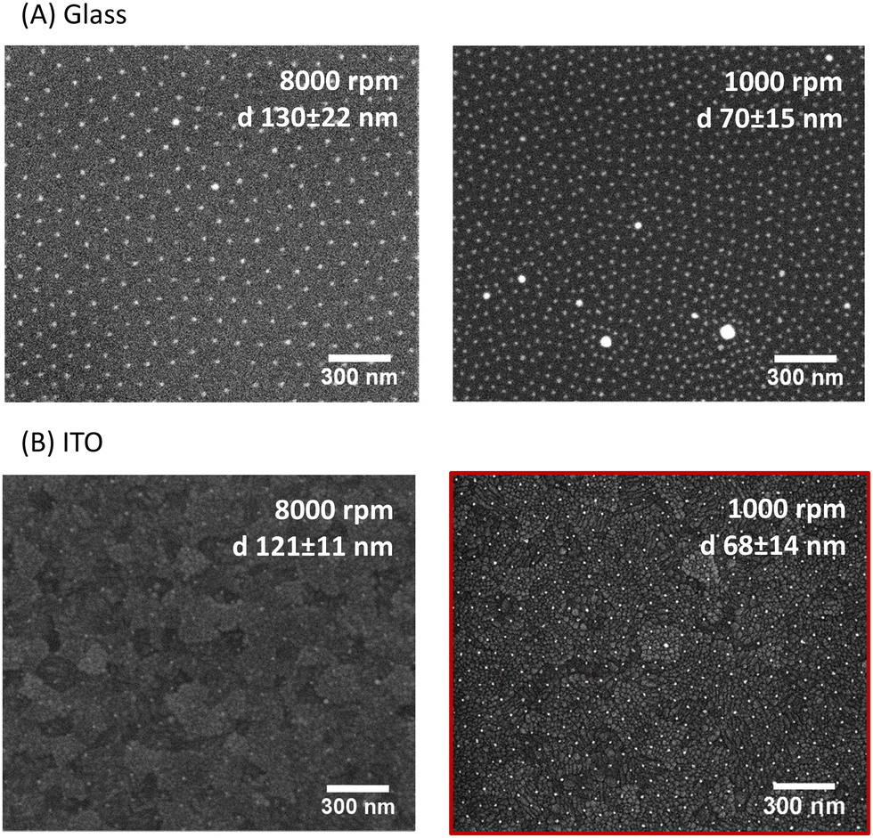 | ||
| Fig. 2 Representative SEM images of (A) glass and (B) ITO substrates with AuNPs deposited by block-copolymer micellar lithography at two different spinning speeds, showing smaller average distances between gold particles (d), as the velocity decreases. | ||
We found that for both glass and ITO surfaces, the lower the spin-coating speed, the smaller the inter-particle distance. The optimal condition to obtain the smallest distance between AuNPs of ca. (68 ± 14) nm on ITO was spinning at 1000 rpm (Fig. 2B). Additionally, the quasi-hexagonal pattern was less regular on ITO than on glass (Fig. 2A), most likely because ITO is more than four times rougher than glass (Fig. S1, ESI†). This makes this step more challenging to achieve reproducible distances between particles.
The second step of the substrate preparation involves the electrodeposition of metallic Au for the overgrowth of the AuNPs, to decrease the inter-particle distance (d). Two different voltages, −0.6 V and −1.0 V, were tested using increasing deposition times. Fig. 3A summarizes the best results obtained for the processing of the pre-patterned ITO (i.e., with the quasi-hexagonal array of AuNPs) at different times by applying −0.6 V. The processing applying −1.0 V at increasing times was also evaluated (Fig. S2, ESI†). To assess the effect of having the pre-patterned AuNPs on ITO, we have also used a bare ITO substrate to directly electrodeposit gold on top, yielding the Au@ITO substrate (Fig. 3B). The electrodeposition was performed using a three-electrode cell with a silver electrode as the reference electrode (RE), a platinum wire as the counter electrode (CE), and the ITO glass substrate (with or without AuNPs) as the working electrode (WE). A 0.5 mM aqueous solution of HAuCl4 was used as an electrolyte to overgrow the particles. From SEM images, it was determined that the optimal processing condition is the application of a voltage of −0.6 V for 600 s. Longer times up to 800 s were also evaluated (Fig. S3, ESI†), obtaining non-homogeneous structures and, thus, verifying the ideal conditions found for 600 s.
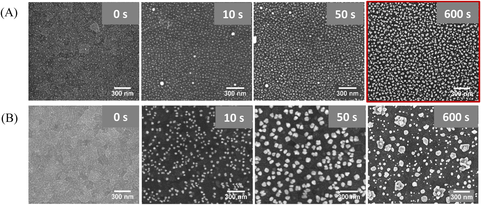 | ||
| Fig. 3 Representative SEM images illustrating the optimization of the Au electrodeposition time at a constant voltage (−0.6 V) for (A) AuNPs pre-patterned on an ITO substrate and (B) on a bare ITO substrate, using an aqueous solution of HAuCl4. Images are displayed in order of increasing times from left to right. | ||
Fig. 4 displays the SEM images of the three different substrates which were used for comparison. The Au–Au distances were averaged by taking 200 distances randomly throughout the entire image (red histograms). The particle size distributions were also estimated (blue histograms) by applying Feret's diameter approximation, which takes the longest distance between any two points within the irregularly shaped particles as its diameter. This probably leads to a slight overestimation of the diameter but is a better approximation than assuming that the particles are perfectly round. For a better visualization of the particles morphology, SEM micrographs with higher magnification are provided in the SI (Fig. S4, ESI†).
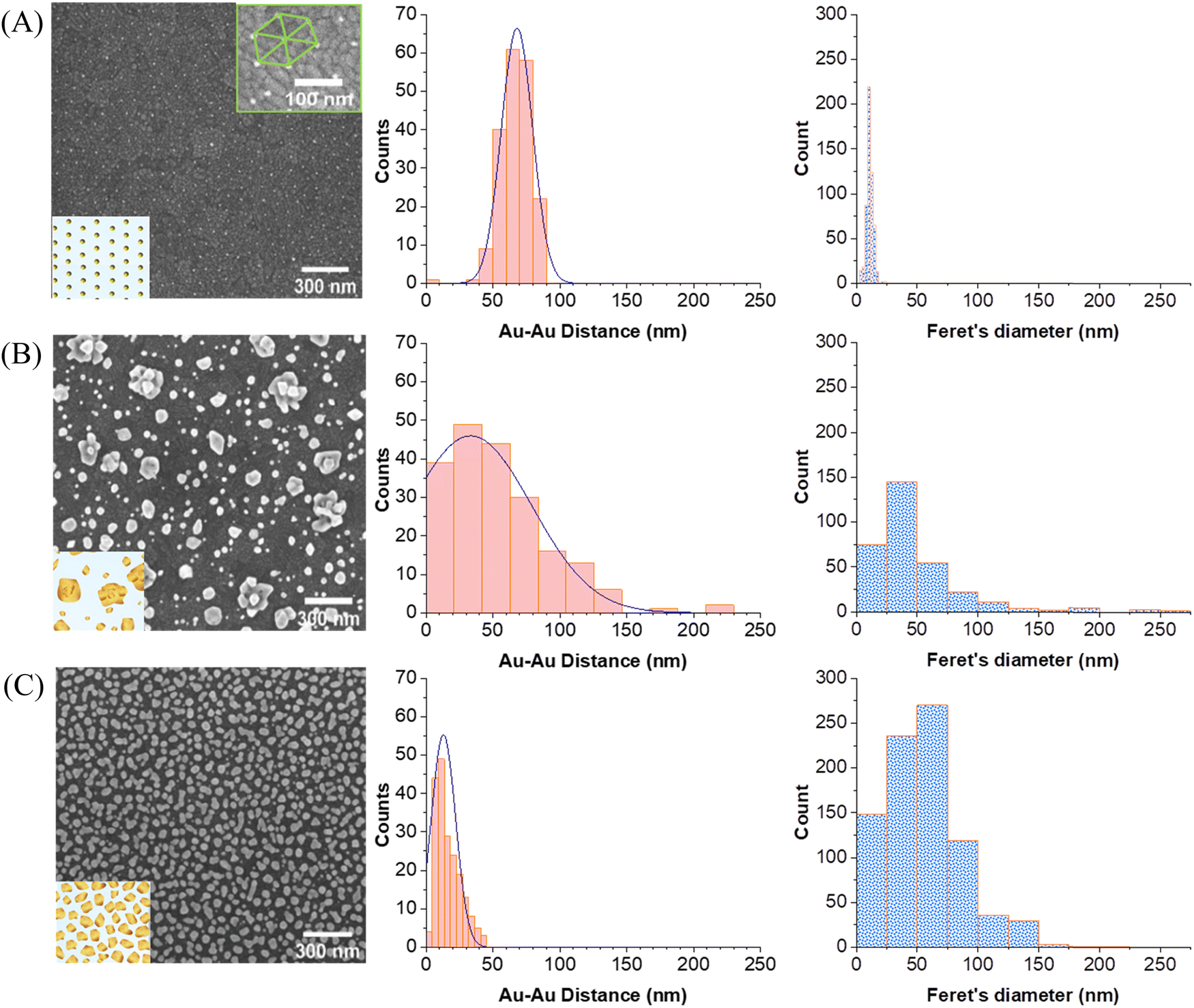 | ||
| Fig. 4 SEM images, Au–Au inter-particle distance (red histograms) and average diameter of gold particles (blue histograms) of (A) an ITO substrate with a quasi-hexagonal pattern of AuNPs deposited by block-copolymer micellar lithography (AuNPs/ITO substrate); (B) Au electrodeposited directly on bare ITO (Au@ITO substrate) and (C) a patterned ITO substrate with quasi-hexagonal AuNPs and further overgrowth of Au by electrodeposition (Au@AuNPs/ITO). | ||
Fig. 4A represents the AuNPs deposited by block-copolymer micellar lithography on ITO (AuNPs/ITO substrate), exhibiting a high homogeneous particle separation of around (68 ± 14) nm. The results of the electrodeposition of Au directly on bare ITO (Au@ITO substrate) are depicted in Fig. 4B, where the average inter-particle distance is very inhomogeneous at (34 ± 54) nm. Fig. 4C shows the resulting substrate developed as a SERS-active substrate following the two-step procedure (Au@AuNPs/ITO substrate). As reflected by the histogram, the distance between particles has been substantially reduced to an average of (15 ± 5) nm, which indicates its suitability as an SERS substrate, as there will be many ideal distances for SERS in the range of 10–20 nm and below. Moreover, the particle size is different for each substrate, being (11 ± 2) nm for the AuNP seeds, (55 ± 114) nm for gold directly electrodeposited on ITO (Au@ITO), and (56 ± 3) nm after the Au overgrowth step (Au@AuNPs/ITO), as shown in Fig. 4A–C, respectively. This increment in size will favour the appearance of local hot spots and surface-plasmon resonance (SPR) signals because very small particles on top of a substrate do not give a detectable SPR.32,42 In this regard, the covered area by gold increases for the different substrates analyzed being 2.5% for AuNPs/ITO, 23% for Au@ITO and 42% for Au@AuNPs/ITO.
To ensure that the deposited Au particles present electrical contact with the ITO and the substrate is still conductive after the gold electrodeposition step, the surface coverage of gold was analyzed. Consequently, gold was functionalized with the switchable electroactive model molecule 11-(ferrocenyl)-undecanethiol (FcC11SH) taking advantage of its thiol end group. Molecules with a thiol functional group will attach preferably to Au because the S–Au bond is very stable (∼50 kcal mol−1),43 forming a self-assembled monolayer (SAM). Such a spontaneous organization of thiolate organic molecules on the gold surface allows for tailoring the surface properties at will.44 After functionalization overnight immersing the substrate in a solution containing the target molecules, cyclic voltammetry was performed to ensure that the deposited Au is in electrical contact with the ITO and to determine if the switchable FcC11SH molecules were covalently attached to the gold. A bare Au/glass substrate with a 200 nm thick layer of gold was used as a reference substrate. The cyclic voltammetry measurements demonstrate that the deposited Au is indeed in electrical contact with the ITO. Furthermore, the fact that the current vs. scan-rate curves show a linear dependence (Fig. S5A, B and D, ESI†) is indicative that the molecules have been effectively adsorbed on the working electrode.45 Thus, the FcC11SH SAM is anchored and stable on each of the three substrates, namely Au/Glass, AuNPs/ITO and the developed Raman-active substrate Au@AuNPs/ITO (Fig. 5A, B and D, respectively). In contrast, Au directly electrodeposited on ITO (Au@ITO) substrate does not show clear redox peaks shifting with the scan rate. This is indicative of a non-stable electrical contact of the electrodeposited Au with the ITO, together with the FcC11SH molecules; which is translated to a non-linear relation of the current vs. scan rate (Fig. S5C, ESI†). From all these voltammogram curves, the gold surface coverages have been calculated, which agree with the expected increment of the gold area for each substrate (Table S1, ESI†).
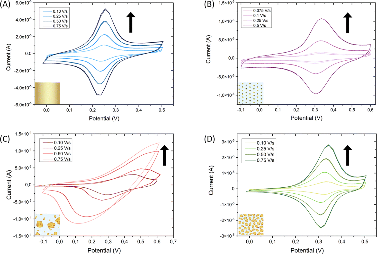 | ||
| Fig. 5 Cyclic voltammogram of 11-(ferrocenyl)-undecanethiol molecules attached to (A) a 200 nm thick layer of gold on glass (Au/Glass), (B) AuNPs on ITO substrates (AuNPs/ITO), (C) Au electrodeposited directly on ITO substrate (Au@ITO), and (D) Au electrodeposited on ITO substrate pre-patterned with AuNPs (Au@AuNPs/ITO). Arrows indicate the direction of the increasing scan rate. TBAPF6 0.1 M in ACN was employed as an electrolyte solution. | ||
To evaluate the electrical robustness of the Au-ITO contact and the anchored molecules on the Au@AuNPs/ITO substrates, 40 switching cycles were performed at a constant scan rate of 0.1 V s−1 which showed high reversibility and reproducibility (Fig. S6, ESI†). We point out that the results shown in Fig. 4 for one Au@AuNPs/ITO SERS substrate are representative of a large set of substrates (more than 50) and provide strong evidence of the high reproducibility of our fabrication process. A statistical analysis of this set yields an Au–Au mean distance and the gold coverage average values of (15 ± 5) nm and (40 ± 5) %, respectively.
Raman measurements were carried out to benchmark the suitability of the different substrates for SERS spectroscopy, comparing the four substrates characterized above, namely, the AuNPs/ITO, Au@ITO, Au@AuNPs/ITO, and Au/Glass substrates. By analyzing them, we demonstrate that the Au@AuNPs/ITO substrate exhibits the best SERS performance. In addition, both reproducibility and homogeneity of the SERS signal in such substrate outperform that of the others, being therefore, ideal for SERS experiments.
For SERS characterization, all four substrates were functionalized with a conventional Raman tag molecule, 4-mercaptobenzoic acid (4-MBA), whose Raman spectrum is well known (Fig. S7A and B, ESI†) and has a thiol end group to form stable SAMs on Au. As with other standard SERS tags, 4-MBA shows intense SERS-activated vibrational bands, mainly ascribed to the aromatic ring contribution. The peaks apparent in the Raman spectrum at 1070 cm−1 and 1580 cm−1, both associated with ring breathing modes,46 were chosen to identify the 4-MBA molecules, as they are the most prominent ones. Their intensity was employed to assess the SERS performance of the four different substrates.
After incubation of the substrates with the Raman tag molecule to form the self-assembled monolayers, SERS measurements were carried out in a 10 × 10 μm2 area. The scans of 40 × 40 points using a 100× microscope objective and the 633 nm laser line with 2.5 mW excitation power (the 633 nm laser was chosen because it yielded the best results, see the ESI†) were performed. Thus, each Raman spectrum at each measurement point was collected using an integration time of 0.5 s. Raman maps were obtained from the corresponding large-area scans, by monitoring the peaks at 1070 cm−1 and 1580 cm−1 of the 4-MBA molecule and collecting the spectrum every 250 nm over the whole 2D image. Both, the continuous gold surface of the Au/Glass substrate and the AuNPs/ITO substrate did not yield any measurable Raman signal, due to the lack of SERS hot spots. In the first case, this is due to the high flatness of the gold surface, as it was deposited directly on glass (see the AFM profile in Fig. S1, ESI†) and, consequently, there are no hot spots (Fig. S7C, ESI†). In the second case, the AuNPs/ITO substrate presents fairly small particles (11 ± 2 nm in diameter) separated by big distances (68 ± 14) nm, hence, not leading to SERS either (Fig. S7D, ESI†).
In the case of Au@ITO and Au@AuNPs/ITO substrates, both show a SERS signal associated with the 4-MBA Raman fingerprint. Several random areas of each substrate were evaluated, and the results are summarized in Fig. 6. The distribution of hot spots for the Au@ITO substrates is not homogeneous over the scanned area (Fig. 6A), which can be explained by the inhomogeneity of gold nanoparticles with a large deviation in particle diameter (55 ± 114) nm. For this reason, some analyzed spots on the substrates do not give a detectable signal for 4-MBA (purple spectrum). Conversely, the substrate that we have developed as a useful tool for large-area homogeneous SERS analysis clearly shows an enhancement of the signal all over the scanned area. Raman maps exhibit highly uniform colors (Fig. 6B), which demonstrates the improved performance of these substrates for SERS with hot spots distributed homogeneously all over the substrate. Both the spectra of two different regions, highlighted in the map (red and purple squares), show the SERS signal, where the 4-MBA characteristic peaks can be easily distinguished.
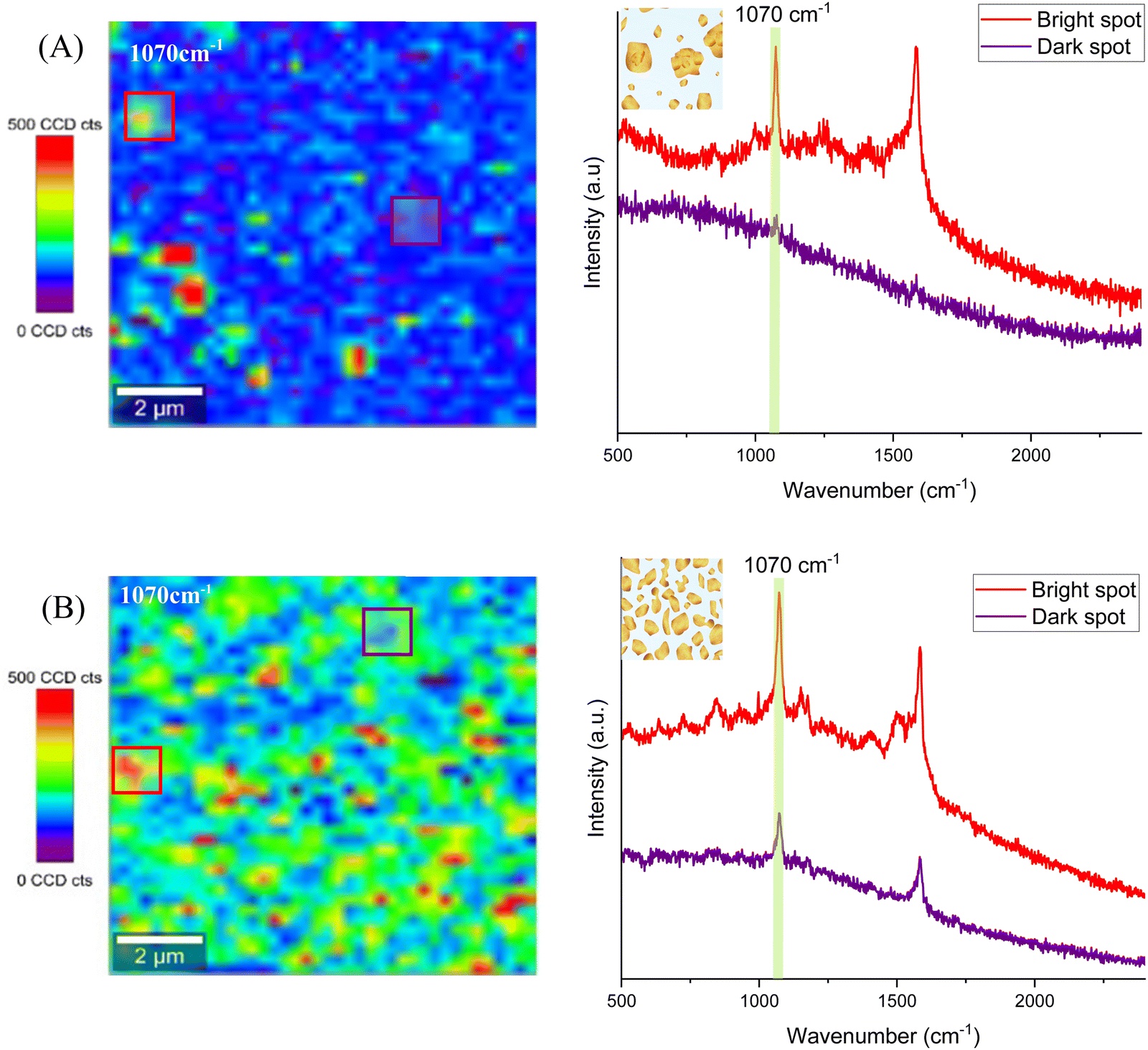 | ||
| Fig. 6 Raman maps of 4-MBA molecules at 1070 cm−1 measured on the (A) electrodeposited gold on ITO substrate (Au@ITO) and (B) Au@AuNPs/ITO substrate. The right panels show representative spectra obtained by integrating the Raman signal inside the square of the corresponding color in the maps comparing strong hot spot areas (red) with moderate hot spots (purple) for each substrate. | ||
To illustrate the uniformity of the signal on the four substrates, Fig. 7 represents the signal-to-noise ratio between the intensity of the 1580 cm−1 peak with respect to the noise. The bright spots (red) represent the stronger intensity of the scanned area, whereas the dark spots (purple) are regions over the same scanned area with a lower Raman intensity.
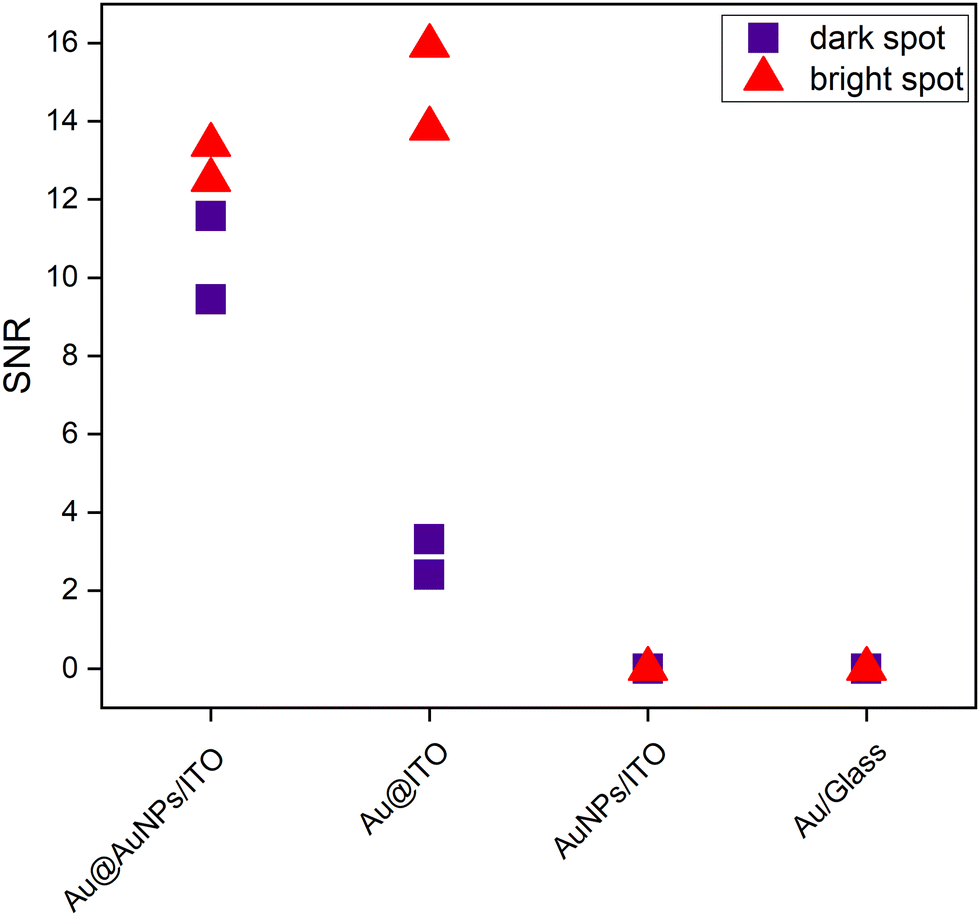 | ||
| Fig. 7 Plot of the signal-to-noise ratio at 1580 cm−1 for the different prepared substrates, functionalized with 4-MBA, in arbitrary points of the measured area for the highly homogeneous conductive Au@AuNPs/ITO substrates and the Au@ITO; AuNPs/ITO and the Au/Glass substrates. The label “dark/bright spot” represents areas on the scanned map with low/high SERS signals, respectively. | ||
In addition, the histograms in Fig. S8 of the ESI† provide a graphical representation of the intensity distribution measured in the Raman maps of the different substrates studied in this work. On the developed substrate Au@AuNPs/ITO (Fig. S8A, ESI†), the spots with high intensity are found more frequently (i.e., on a larger number of pixels) compared to the other substrates, in which most of the pixels are associated with the lower intensities. Supporting these results, a quantitative study of the homogeneity of the substrates on a middle-to-large scale was carried out. Additionally, the variability of the SERS enhancement on substrates Au@ITO and Au@AuNPs/ITO was evaluated using the 4-MBA SERS signal, as summarized in Table S2 of the ESI.† The pre-patterned substrate (Au@AuNPs/ITO) features the best performance showing the lowest variability over the different area ranges (from ∼1 μm to ∼100 μm), confirming that the developed substrate presents an important improvement regarding SERS homogeneity and reproducibility.
Finally, to exploit the conductive characteristics of the developed homogeneous Au@AuNPs/ITO SERS substrates, their discrete gold surfaces were grafted with the electroactive redox thiolate hydroquinone (HQC4SH) to monitor the switching behavior using Raman-SERS signal as output. The interfacial reactions involving the grafted quinone molecules that may occur are schematically depicted in Fig. 8. The SERS signal of the hydroquinones is mainly ascribed to the aromatic ring, whereas this signal is absent in benzoquinones. It is important to remember that the longer the lateral chain of the hydroquinone, the smaller will be the available SERS enhancement, as the electric field amplification in SERS decreases exponentially with the distance to the “hot-spot”. For this reason, we are using a short (four carbons) chain. The use of a twelve carbons lateral chain was evaluated but no SERS signal was detected.
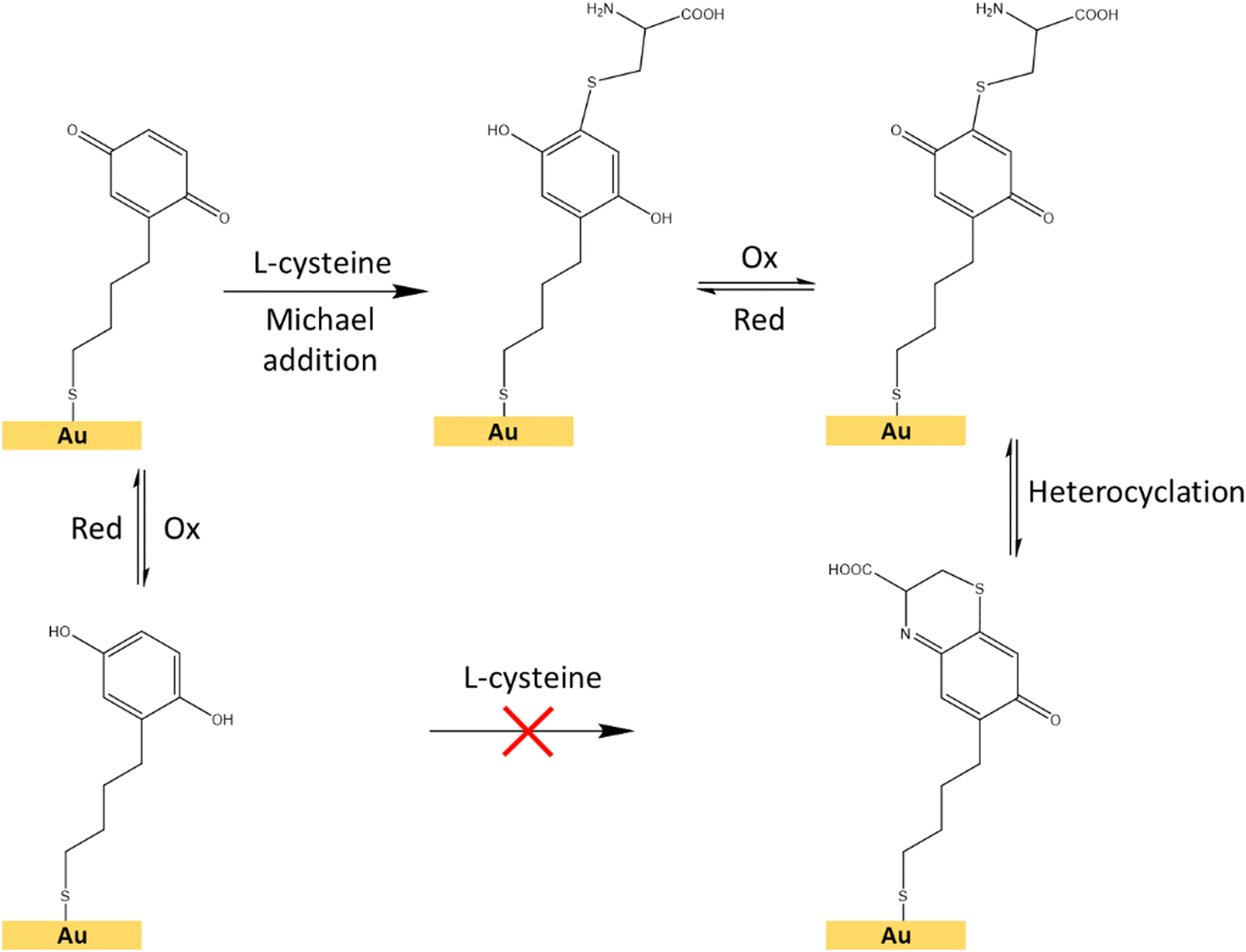 | ||
| Fig. 8 Schematic representation of the interfacial Michael addition reaction between the hydroquinone/benzoquinone redox pair and the L-cysteine molecule on a surface.48 | ||
For the electrochemical-SERS measurements, we followed the interfacial Michael addition reaction between the grafted hydroquinone molecules with the biologically relevant analyte L-cysteine. This reaction only takes place in the benzoquinone state (oxidized state of hydroquinone) (Fig. 8).47,48L-Cysteine is an amino acid found naturally in the human body and one of the amino acids that are building blocks of the powerful antioxidant glutathione. It is also found in many protein-rich foods and is sold as a dietary supplement. The electrochemical-SERS measurement will provide direct spectroscopic evidence of the presence of the oxidation state and the analyte, through the structural changes occurring in such reaction in real-time.
First, we followed the electrochemical induced reaction between the L-cysteine with the hydroquinone/benzoquinone redox pair, in solution, by cyclic voltammetry (Fig. S9, ESI†). As shown in the ESI,† the reaction only takes place when the hydroquinone is first oxidized to benzoquinone, subsequently reacting with L-cysteine (Fig. 8), but this reaction does not occur between the reduced form, i.e. the hydroquinone.
Then, we repeated the procedure with the molecules forming SAMs and combined cyclic voltammetry with SERS. We functionalized overnight the gold surfaces of Au@AuNPs/ITO with a solution of HQC4SH in ethanol. Cyclic voltammetry measurements were performed to confirm that the redox molecules were covalently attached forming a stable SAM. Indeed, the oxidation and reduction peaks were visible at +0.18 V and −0.03 V, respectively (Fig. S10 left, ESI†) which show a linear dependence of the current with increasing scan rates up to 1 V s−1 (Fig. S10 right, ESI†). This confirms that the molecules are strongly anchored to the substrate and stable over time.
To demonstrate the suitability of the developed substrates for electrochemical-SERS experiments, the different electronic states of the SAMs were followed by SERS. The cyclic voltammetry and SERS spectra were first acquired for the hydroquinone SAM (Fig. 9 left, garnet curve). The cyclic voltammetry of the hydroquinone shows an adequate voltammogram, with the reduction and oxidation peaks at the expected voltage. Thanks to the stability of the SAMs, it was possible to measure the SERS spectrum after recording the voltammogram. The garnet Raman spectrum shown in Fig. 9 (right) is an average of the more frequent “hot-spots” signals, over the scanned area, with two main peaks centred at 1257 cm−1 and 1450 cm−1. Hereafter, the same substrate was immersed into a 3-electrode electrochemical cell for the oxidation of the hydroquinone SAM into benzoquinone, by applying +0.4 V for 600 s. The cell contained L-cysteine in solution for the interfacial Michael addition reaction with the oxidized benzoquinone. Afterward, the voltammetric and SERS signals were again acquired. The reaction between L-cysteine and benzoquinone is confirmed in the electrochemical signal by a decrease in the intensity of the voltammogram after applying a positive potential (Fig. 9 left, red curve). Since the SAM is not electroactive anymore after the reaction with L-cysteine, a close-ring structure is proposed as a result of the interfacial reaction (Fig. 8).
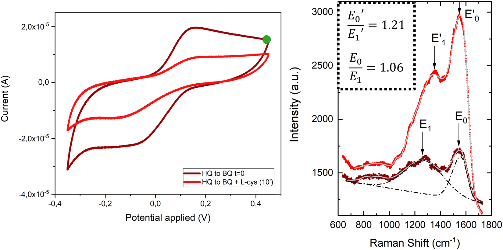 | ||
| Fig. 9 Left: Cyclic voltammogram of a hydroquinone/benzoquinone SAM on the Au@AuNPs/ITO surface before (garnet) and after (red) its oxidation during 600 s at +0.4 V (green dot), in the presence of L-cysteine. Voltammograms were acquired using a 3-electrode setup with Au@AuNPs/ITO as the WE, Pt as the CE, Ag/AgCl as the RE and PBS as the electrolyte at a scan rate of 0.1 V s−1. Right: Raman average spectra corresponding to the hydroquinone/benzoquinone SAM on the Au@AuNPs/ITO surface before (garnet) and after (red) its oxidation at +0.4 V and subsequent reaction with L-cysteine. Inset: Ratios between the two main peaks of this spectrum, E0/E1 and E0′/E1′. | ||
Right after the oxidation to benzoquinone and the resulting interfacial reaction with L-cysteine, the SERS spectrum of the Au@AuNPs/ITO substrate was measured (Fig. 9 right, red spectrum). Clear changes in the average SERS spectra are observable, namely an increase of the overall SERS intensity, a shift of the 1257 cm−1 peak to higher wavenumbers (1357 cm−1), and a significant increase in the intensity ratio (E0/E1) between the two main peaks. The latter increased from 1.06 to 1.21 after the reaction between the benzoquinone SAM and the L-cysteine took place (see inset to Fig. 9). The changes in the Raman spectra are associated with variations in different stretching modes of the C–C single and C![[double bond, length as m-dash]](https://www.rsc.org/images/entities/char_e001.gif) C double bond modes of the quinone ring, which are different after the interfacial reaction with the L-cysteine molecule. Thus, SERS measurements on the surface go along with the voltammograms recorded for the proposed reaction in solution (Fig. S9, ESI†). These results demonstrate the capability of the conductive SERS-active Au@AuNPs/ITO substrates to successfully perform electrochemical-SERS experiments like the monitoring of switchable redox molecules and their modification upon variable electrochemical inputs.
C double bond modes of the quinone ring, which are different after the interfacial reaction with the L-cysteine molecule. Thus, SERS measurements on the surface go along with the voltammograms recorded for the proposed reaction in solution (Fig. S9, ESI†). These results demonstrate the capability of the conductive SERS-active Au@AuNPs/ITO substrates to successfully perform electrochemical-SERS experiments like the monitoring of switchable redox molecules and their modification upon variable electrochemical inputs.
Conclusions
Combining the block-copolymer micellar lithography (BCML) technique for generating homogeneously distributed, quasi-hexagonal arrays of AuNPs, on a transparent and conductive ITO surface, with the overgrowth of these AuNPs by a controlled gold electrodeposition, is an attractive method to prepare highly homogeneous and robust SERS-active and conductive surfaces with a large gold coverage area of ca. 40%. These substrates show many hot spots due to a small mean inter-particle distance of ca. 15 nm, which are homogeneously distributed across the surface. These surfaces were thoroughly characterized for their SERS capability by a detailed analysis of the Raman signals using the standard Raman tag molecule 4-mercaptobenzoic acid to form a SAM on the gold particle surfaces, reinforced by a quantitative analysis of the homogeneity. Moreover, electrochemical investigation combined with SERS enables monitoring the evolution of an electroactive double-state molecular switch and the reaction of one of its redox states with a biologically relevant analyte using the Raman signal as the output signal. These results open up the way to the use of our substrates for sensing analytes but also to monitor switchable redox molecules for potential molecular logic gates, thus contributing to advance molecule-based electronic devices.Conflicts of interest
There are no conflicts to declare.Materials and methods
ITO Glass Substrates (S111, 20 × 15 mm; 1.1 mm thickness; sheet resistance 20 Ω sq−1) were purchased from Ossila Ltd (Sheffield, UK). Gold(III) chloride trihydrate (HAuCl4·3H2O) was purchased from Sigma-Aldrich Co (or Merck group). All reagents were analytical grade and used as received without any further purification. Polymers were purchased from Polymer Source Inc. (Canada). All solvents used were purchased from Merck group, if not specified.All glass materials used were previously cleaned using piranha solution (concentrated sulfuric acid 96% with hydrogen peroxide 30%, (3![[thin space (1/6-em)]](https://www.rsc.org/images/entities/char_2009.gif) :1 v/v).
:1 v/v).
Block-copolymer micellar lithography
ITO glass substrates were cleaned by sonication in acetone for 20 min at 50 °C followed by rinsing with copious amounts of Milli-Q® water. ITO substrates were then sonicated in a 5:1:1 mixture of H2O:H2O2 (20%):NH4OH (27%) for 15 min at 70 °C. The next step was to sonicate in Milli-Q® water three times for a few minutes, replaced with new water each time. Finally, ITO substrates were dried under a nitrogen stream.
Block-copolymer micellar lithography was performed as described elsewhere.28–30 The copolymer polystyrene-block-poly-2-vinylpyridine (PS (106000)-b-P2VP (75000)) was dissolved in anhydrous toluene (previously dried over activated 3 Å molecular sieves for 24 h) at a concentration of 2 mg mL−1 and stirred during 24 h. Afterward, HAuCl4·3H2O was added to load the micelles (2.5 mM) and the suspension was stirred for 24 h.
A volume of 21 μL of Au-loaded micelles was spin-coated on ITO glass substrate at 1000 rpm for 1 min and 10 s (spin coater model WS400BZ-6NPP LITE). After spin-coating, substrates were treated with oxygen plasma at 150 W, 0.4 mbar for 45 min (model PS210) to remove the polymer and reduce gold to metallic nanoparticles forming a quasi-hexagonal array.
Growth of AuNPs by electrodeposition
Electrochemical experiments were performed with a potentiostat PGSTAT204 and the software used for data acquisition and analysis was Nova 2.3. A three-electrode electrochemical cell was used, with a silver wire as the reference electrode (RE), platinum wire as the counter electrode (CE) and ITO glass substrates (with or without AuNPs) as working electrode (WE); the immersed area into electrolyte solution was approximately 1.5 cm2.Quasihexagonal arrays of gold nanoparticles on ITO substrates were enlarged with further gold by chronoamperometry. For that, AuNPs-ITO Substrates were previously cleaned by rinsing with EtOH to eliminate any impurities and were activated under UV-O3 for 20 min, during this time an aqueous solution of HAuCl4 at a concentration of 0.5 mM was prepared. Then, 10 mL of HAuCl4 was added to the electrochemical cell and nitrogen was flowed through for a few minutes to displace oxygen from the solution. The nanostructured substrate was connected as the WE and merged into the electrolyte solution. The experiment was carried out using the chronoamperometry technique applying a voltage of −0.6 V for 600 s. Once the process was completed the substrates were cleaned with Milli-Q® water a couple of times and dried with nitrogen gas.
Characterization of substrates
For the SERS variability studies, spectroscopic maps with different sampling steps (1–100 μm) were carried out over different sized areas, regularly distributed over a mm2 surface, using a 100× objective and keeping the 633 nm laser power fixed at 500 μW. The SERS variability was monitored at short-range (1 μm distance), medium range (10 μm distance) and long range (100–1000 μm distance).
Acknowledgements
The authors appreciate the financial support of the Spanish Government through the grants MOTHER (MAT2016-80826-R), Mol4Bio (PID2019-105622RBI00), Immunys (PID2020-115296RA-I00) and the “Ramón y Cajal” program (RYC-2017-22614). Additionally, ICMAB acknowledges support from the Spanish Ministry of Science and Innovation through the “Severo Ochoa” Programme for Centres of Excellence in R & D (CEX2019-000917-S). The authors are also grateful to the Networking Research Center on Bioengineering, Biomaterials and Nanomedicine (CIBER-BBN; projects “Alycia” (No. BBN18PI01) and “Gels4ACT” (No. BBN20PIV02)). Fundació Marató de TV3 (No. 201812) and Generalitat de Catalunya (SGR Cat 2021 - 00438) are also acknowledged. The work was funded as well by the Max Planck Society through the Max Planck Partner Group “Dynamic Biomimetics for Cancer Immunotherapy” in collaboration with the Max Planck for Medical Research (Heidelberg, Germany). N. G. P. is enrolled in the Materials Science PhD program of Universitat Autònoma de Barcelona (UAB) and acknowledges the financial support from the FPU fellowship (FPU17/02551) from the Spanish Ministry. N. P. acknowledges Regione Lazio for financial support for the stay at ICMAB through the “Torno Subito” programme.References
- E. C. Le Ru and P. G. Etchegoin, Principles of Surface Enhanced Raman Spectroscopy (and related plasmonic effects), Elsevier, Amsterdam, 2009 Search PubMed.
- R. A. Alvarez-Puebla and L. M. Liz-Marzán, Small, 2010, 6, 604–610 CrossRef CAS PubMed.
- E. Cortés, P. G. Etchegoin, E. C. Le Ru, A. Fainstein, M. E. Vela and R. C. Salvarezza, J. Am. Chem. Soc., 2010, 132, 18034–18037 CrossRef PubMed.
- B. Sharma, R. R. Frontiera, A. Henry, E. Ringe and R. P. Van Duyne, Mater. Today, 2012, 15, 16–25 CrossRef CAS.
- R. S. Das and Y. K. Agrawal, Vib. Spectrosc., 2011, 57, 163–176 CrossRef CAS.
- L. Osinkina, T. Lohmüller, F. Jäckel and J. Feldmann, J. Phys. Chem. C, 2013, 117, 22198–22202 CrossRef CAS.
- S. Lu, T. You, Y. Gao, N. Yang, C. Zhang and P. Yin, Spectrochim. Acta, Part A, 2019, 212, 371–379 CrossRef CAS PubMed.
- S. Su, Y. Wu, D. Zhu, J. Chao, X. Liu, Y. Wan, Y. Su, X. Zuo, C. Fan and L. Wang, Small, 2016, 12, 3794–3801 CrossRef CAS PubMed.
- C. Liu, J. Wu, S. Wang and J. Fang, J. Electroanal. Chem., 2022, 909, 116120 CrossRef CAS.
- A. A. Tseng, K. Chen, C. D. Chen and K. J. Ma, IEEE Trans. Electron. Packag. Manuf., 2003, 26, 141–149 CrossRef CAS.
- L. Jiang, M. M. Hassan, S. Ali, H. Li, R. Sheng and Q. Chen, Trends Food Sci. Technol., 2021, 112, 225–240 CrossRef CAS.
- B. H. C. Greene, D. S. Alhatab, C. C. Pye and C. L. Brosseau, J. Phys. Chem. C, 2017, 121, 8084–8090 CrossRef CAS.
- D. Ibáñez, A. Pérez-junquera, M. B. González-garcía, D. Hernández-santos and P. Fanjul-bolado, Talanta, 2020, 206, 120190 CrossRef PubMed.
- C. N. Hernández, D. Martín-yerga, M. B. González-garcía, D. Hernández-santos and P. Fanjul-bolado, Talanta, 2018, 178, 85–88 CrossRef PubMed.
- Y. Teng, Z. Ren, Y. Zhang, Z. Wang, Z. Pan, K. Shao and Y. She, New J. Chem., 2020, 44, 1777–1784 RSC.
- M. Tsai, Y. Lin and S. Luo, ACS Appl. Mater. Interfaces, 2019, 11, 1402–1410 CrossRef CAS PubMed.
- S. Zaleski, M. F. Cardinal, J. M. Klingsporn and R. P. Van Duyne, J. Phys. Chem. C, 2015, 119, 28226–28234 CrossRef CAS.
- W. F. Paxton, S. L. Kleinman, A. N. Basuray, J. F. Stoddart and R. P. Van Duyne, J. Phys. Chem. Lett., 2011, 2, 1145–1149 CrossRef CAS PubMed.
- C. Simão, M. Mas-Torrent, J. Casado-Montenegro, F. Otón, J. Veciana and C. Rovira, J. Am. Chem. Soc., 2011, 133, 13256–13259 CrossRef PubMed.
- M. Souto, J. Guasch, V. Lloveras, P. Mayorga, J. T. López Navarrete, J. Casado, I. Ratera, C. Rovira, A. Painelli and J. Veciana, J. Phys. Chem. Lett., 2013, 4, 2721–2726 CrossRef CAS.
- M. Souto, H. Cui, M. Peña-Álvarez, V. G. Baonza, H. O. Jeschke, M. Tomic, R. Valentí, D. Blasi, I. Ratera, C. Rovira and J. Veciana, J. Am. Chem. Soc., 2016, 138, 11517–11525 CrossRef CAS PubMed.
- M. Souto, L. Yuan, D. C. Morales, L. Jiang, I. Ratera, C. A. Nijhuis and J. Veciana, J. Am. Chem. Soc., 2017, 139, 4262–4265 CrossRef CAS PubMed.
- S. Sreejith and A. Ajayaghosh, Indian J. Chem., Sect. A: Inorg., Bio-inorg., Phys., Theor. Anal. Chem., 2012, 51, 47–56 Search PubMed.
- I. Ratera, J. Vidal-Gancedo, D. Maspoch, S. T. Bromley, N. Crivillers and M. Mas-Torrent, J. Mater. Chem. C, 2021, 9, 10610–10623 RSC.
- X. Dai and R. G. Compton, Anal. Sci., 2006, 22, 3212 Search PubMed.
- Y. Hu, Y. Song, Y. Wang and J. Di, Thin Solid Films, 2011, 519, 6605–6609 CrossRef CAS.
- J. Langer, D. J. De Aberasturi, J. Aizpurua, R. A. Alvarez-puebla, B. Auguie, J. J. Baumberg, G. C. Bazan, S. E. J. Bell and A. Boisen, ACS Nano, 2020, 14, 28–117 CrossRef CAS PubMed.
- J. Guasch, M. Hoffmann, J. Diemer, H. Riahinezhad, S. Neubauer, H. Kessler and J. P. Spatz, Nano Lett., 2018, 18, 5899–5904 CrossRef CAS PubMed.
- J. Guasch, C. A. Muth, J. Diemer, H. Riahinezhad and J. P. Spatz, Nano Lett., 2017, 17, 6110–6116 CrossRef CAS PubMed.
- J. Guasch, J. Diemer, H. Riahinezhad, S. Neubauer, H. Kessler and J. P. Spatz, Chem. Mater., 2016, 28, 1806–1815 CrossRef CAS.
- R. Glass, M. Möller and J. P. Spatz, Nanotechnology, 2003, 14, 1153–1160 CrossRef CAS.
- P. K. Jain, K. S. Lee, I. H. El-Sayed and M. A. El-Sayed, J. Phys. Chem. B, 2006, 110, 7238–7248 CrossRef CAS PubMed.
- B. Landeke-Wilsmark, L. Nyholm and C. Hägglund, Langmuir, 2020, 36, 6848–6858 CrossRef CAS PubMed.
- H. H. Jeong, M. C. Adams, J. P. Günther, M. Alarcón-Correa, I. Kim, E. Choi, C. Miksch, A. F. Mark, A. G. Mark and P. Fischer, ACS Nano, 2019, 13, 11453–11459 CrossRef CAS PubMed.
- A. Alvarez-Fernandez, C. Cummins, M. Saba, U. Steiner, G. Fleury, V. Ponsinet and S. Guldin, Adv. Opt. Mater., 2021, 9, 2100175 CrossRef CAS.
- W. J. Cho, Y. Kim and J. K. Kim, ACS Nano, 2012, 6, 249–255 CrossRef CAS PubMed.
- R. F. Pagels, J. Edelstein, C. Tang and R. K. Prud’homme, Nano Lett., 2018, 18, 1139–1144 CrossRef CAS PubMed.
- T. Lohmüller, D. Aydin, M. Schwieder, C. Morhard, I. Louban, C. Pacholski and J. P. Spatz, Biointerphases, 2011, 6, MR1–MR12 CrossRef PubMed.
- D. Aydin, I. Louban, N. Perschmann, J. Blümmel, T. Lohmüller, E. A. Cavalcanti-Adam, T. L. Haas, H. Walczak, H. Kessler, R. Fiammengo and J. P. Spatz, Langmuir, 2010, 26, 15472–15480 CrossRef CAS PubMed.
- B. R. Cuenya, S. H. Baeck, T. F. Jaramillo and E. W. McFarland, J. Am. Chem. Soc., 2003, 125, 12928–12934 CrossRef PubMed.
- D. Pallarola, A. Bochen, V. Guglielmotti, T. A. Oswald, H. Kessler and J. P. Spatz, Anal. Chem., 2017, 89, 10054–10062 CrossRef CAS PubMed.
- H. Tyagi, T. Khan, J. Mohapatra, A. Mitra, H. Kalita and M. Aslam, RSC Adv., 2016, 6, 109192–109200 RSC.
- R. G. N. and and L. H. Dubois, Annu. Rev. Phys. Chem., 1992, 437–463 Search PubMed.
- J. C. Love, L. A. Estroff, J. K. Kriebel, R. G. Nuzzo and G. M. Whitesides, Chem. Rev., 2005, 105, 1103–1169 CrossRef CAS PubMed.
- N. Elgrishi, K. J. Rountree, B. D. McCarthy, E. S. Rountree, T. T. Eisenhart and J. L. Dempsey, J. Chem. Educ., 2018, 95, 197–206 CrossRef CAS.
- A. Capocefalo, D. Mammucari, F. Brasili, C. Fasolato, F. Bordi, P. Postorino and F. Domenici, Front. Chem., 2019, 7, 1–11 CrossRef PubMed.
- A. R. Kyvik, C. Luque-Corredera, D. Pulido, M. Royo, J. Veciana, J. Guasch and I. Ratera, J. Phys. Chem. B, 2018, 122, 4481–4490 CrossRef CAS PubMed.
- J. Li, C. L. Sun, L. Tan, Y. L. Xie and H. L. Zhang, Langmuir, 2013, 29, 5199–5206 CrossRef CAS PubMed.
Footnote |
| † Electronic supplementary information (ESI) available. See DOI: https://doi.org/10.1039/d2ma00914e |
| This journal is © The Royal Society of Chemistry 2023 |