
 Open Access Article
 This Open Access Article is licensed under a
 Creative Commons Attribution 3.0 Unported Licence
Recent advances in strongly resonant and gradient all-dielectric metasurfaces
Dimitrios C.
Zografopoulos
 *a and
Odysseas
Tsilipakos
*bc
*a and
Odysseas
Tsilipakos
*bc
aConsiglio Nazionale delle Ricerche, Istituto per la Microelettronica e Microsistemi (CNR-IMM), Rome 00133, Italy. E-mail: dimitrios.zografopoulos@artov.imm.cnr.it
bTheoretical and Physical Chemistry Institute, National Hellenic Research Foundation, GR-11635 Athens, Greece. E-mail: otsilipakos@eie.gr
cInstitute of Electronic Structure and Laser, Foundation for Research and Technology-Hellas (FORTH-IESL), GR-70013 Heraklion, Greece
First published on 11th November 2022
Abstract
All-dielectric metasurfaces have been intensively researched as a low-loss, flat-optics platform for the advanced manipulation of electromagnetic wave propagation. Among the numerous metasurface-enabled functionalities, particular focus has been recently placed on the engineering of components with an extremely narrowband response, stemming from so-called bound states in the continuum, which can boost the performance of, among others, non-linear, sensing, or lasing devices thanks to the enhanced light–matter interaction and strong field enhancement. On the other extreme in terms of their operating bandwidth, spatially modulated gradient metasurfaces have opened the path towards ultrabroadband, achromatic, flat components, which are key to applications such as imaging, holography, and the processing of ultra-short pulses. In this work, we provide a critical overview of recent developments in both fields, highlighting the underlying physical concepts, reporting their experimental demonstration in a broad range of applications with unprecedented performance, and providing a future outlook towards metasurfaces with extreme spectral responses as the enabling element in emerging applications.
 Dimitrios C. Zografopoulos | Dimitrios Zografopoulos received his PhD in 2009 from the Aristotle University of Thessaloniki (AUTH). Subsequently, he was an AUTH Post-Doctoral Research Fellow (2010), Post-Doctoral Fellow of the Greek States Scholarship Foundation and Visiting Research Fellow at the Department of Electronics Technology, Carlos III University of Madrid (2011). He then moved under a Marie-Curie Fellowship to the Institute for Microelectronics and Microsystems, Italian National Research Council, where he has been working as a researcher. He is the (co)author of ∼100 refereed articles and ∼90 conference proceedings. His research interests focus on resonant dielectric metasurfaces, tunable metadevices and components for terahertz wave manipulation. |
 Odysseas Tsilipakos | Odysseas Tsilipakos obtained his PhD degree from the School of Electrical and Computer Engineering, Aristotle University of Thessaloniki in 2013. From 2016 to 2022 he was a Postdoctoral Fellow at the Institute of Electronic Structure and Laser of the Foundation for Research and Technology Hellas. Since October 2022 he serves as an elected Associate Researcher in the Theoretical and Physical Chemistry Institute of the National Hellenic Research Foundation. He is a (co-)author of ∼50 refereed journal articles and ∼60 international conference publications. His research interests span metasurfaces, plasmonics, nanophotonic resonators and leaky cavities, nonlinear optics, and 2D materials. He is a Senior Member of IEEE and a member of The Optical Society. |
1 Introduction
Metasurfaces, the two dimensional versions of metamaterials,1 have been systematically researched over the last 15 years. With the term “metasurfaces” we broadly refer to thin artificial materials comprised of subwavelength building blocks, termed meta-atoms.2,3 By designing the constituent meta-atoms (geometry and material composition), these sheet materials can inherit interesting and often exotic electromagnetic properties, allowing strong control to be exerted over incident radiation despite their thin nature. Starting from simple uniform structures that are only electrically polarizable, research on metasurfaces has come a long way to include structures with a purposeful spatial modulation, surfaces that exhibit both electric and (artificial) magnetic polarizability, and structures that comprise multiple meta-atoms and/or multiple resonances within the unit cells, to name but a few. These developments have allowed for the demonstration of metasurfaces that can offer control over practically every aspect of the electromagnetic field (amplitude, phase, polarization, wavefront, and frequency content).4–6Recently, metasurfaces have been pushed to the extreme in search of enhanced performance and new application regimes. The emergence of metasurfaces supporting bound states in the continuum (BIC)7–9 has provided a pathway towards achieving a strongly resonant response and an ultra-narrow temporal bandwidth. BIC metasurfaces can offer extreme frequency selectivity and the ability to profoundly enhance the local fields and boost light–matter interaction. Closely related terms are those of trapped, quasi-dark, and broken-symmetry resonances. On the other extreme as regards their operating bandwidth, metasurfaces with a broadband, achromatic response can accommodate ultra-short pulses/wavepackets and enable the realization of optical components that retain their functionality over ultra-wide bands (e.g. metalenses with a constant focal length and minimal chromatic aberrations over the entire visible spectrum). In this review, we document such advances in recent research on metasurfaces. We base the discussion on two overarching functionalities that have implications in a very broad range of applications. More specifically, we first report on sharply resonant metasurfaces that can have a transformational impact in biosensing, nonlinear applications, and nanolasers. We then focus on gradient (i.e., spatially modulated) metasurfaces for wavefront manipulation10,11 (e.g., beam steering/focusing) that can offer significant technological advantages in the fields of communications, imaging, microscopy and holography. Throughout this review, we focus on all-dielectric implementations of metasurfaces, which, especially at higher frequencies (infrared and optical), can be quite a favorable option over metallic/plasmonic counterparts due to reduced resistive losses.
The paper is organized into two parts. Section 2 addresses the recent advances in BIC all-dielectric metasurfaces, including the challenges towards obtaining high quality factors (Section 2.1), and their applications in nonlinear phenomena (Section 2.2), lasing structures (Section 2.3), biosensing (Section 2.4), and other wave-manipulating static (Section 2.5) or tunable (Section 2.6) systems. Section 3 addresses the recent advances in gradient all-dielectric metasurfaces, including metagratings (Section 3.2), achromatic metasurfaces (Section 3.3), and tunable/reconfigurable structures (Section 3.4). The conclusion and outlook is provided in Section 4.
2 Bound states in the continuum in all-dielectric metasurfaces
BICs are discrete, non-radiative states that lie within, but are orthogonal to the radiation continuum. They were initially demonstrated in the context of quantum mechanics, but it was later shown that they regard general wave phenomena observed also in, for instance, acoustics, hydrodynamics, and electromagnetics. Despite the fact that they are localized in space, such resonances are non-decaying (infinite lifetime), which makes them particularly interesting both from a fundamental physics and an applications standpoint.BICs are generally classified into two types: (i) symmetry-protected (SP-BICs) and (ii) accidental (A-BICs). SP-BICs occur at high-symmetry points of the momentum space, the Γ point being the most investigated as it corresponds to normal incidence on a planar structure, such as a periodic metasurface or a photonic crystal slab. Depending on the symmetry of the structure, SP-BICs are eigenmodes located above the light cone and exhibit a different symmetry compared to the impinging wave, hence they cannot be excited and thus remain “dark”. In order for them to manifest in what is termed as quasi-BICs (qBICs), the symmetry system has to be reduced, typically by introducing a (small) degree of geometrical asymmetry; changing the material properties is also an option. In this context, group theoretical analysis can provide clear insight into the modal symmetries, the required symmetry reduction, and the polarization-selective rules for qBIC excitation.12–15
Fig. 1(a) shows a metasurface composed of ellipsoid nanoparticles, which has been extensively investigated as a platform for SP-BIC based applications.16 By tilting the axes of adjacent particles, the BIC mode becomes accessible as a qBIC with increasing linewidth as the asymmetry is increased. In fact, the radiative Q-factor of the system follows an inverse square law Qr ∝ α−2, with α being the degree of asymmetry, a property which characterizes all SP-BIC metasurfaces in the non-diffracting, low-asymmetry regime. This provides a clear design rule in order to match the target linewidth, although non-radiative losses complicate the picture, as will be discussed in the next section. SP-BICs are also accessible for k-vectors different from their symmetry point, usually for an obliquely incident planewave. Fig. 1(b) outlines such a case: a vertically oriented collective magnetic dipole resonance cannot radiate in the plane of the infinite metasurface for normal incidence, but becomes accessible for oblique incidence, which breaks the symmetry of the impinging planewave due to the presence of an in-plane component of the k-vector.17
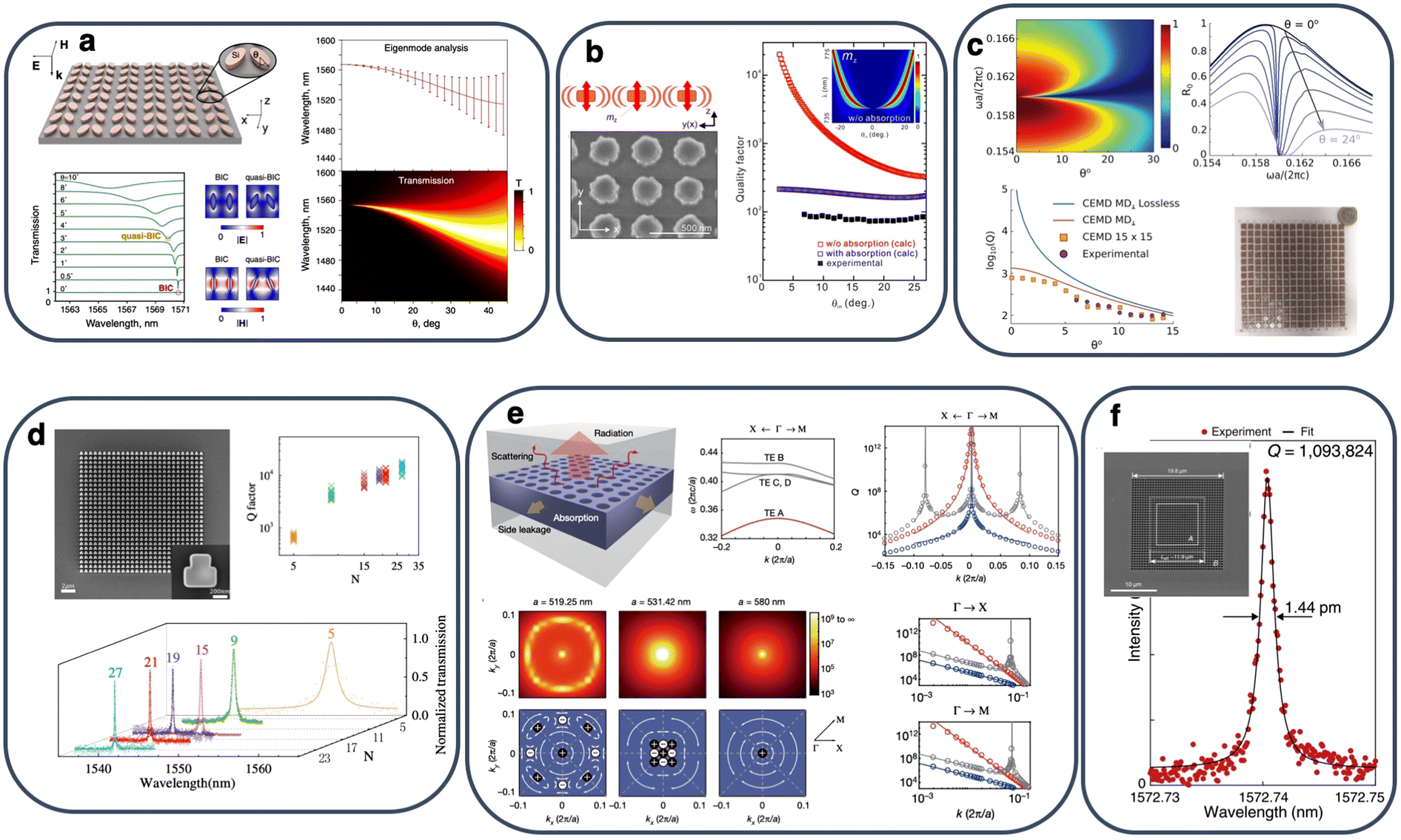 | ||
Fig. 1 (a) A typical SP-qBIC dielectric metasurface composed of ellipsoid nanoparticles where symmetry breaking is controlled by tilting the particle long axis. Reprinted with permission from ref. 16. Copyright 2018 by the American Physical Society. (b) Experimental demonstration of a metasurface resonating with a perpendicular magnetic dipole qBIC mode in Si nanodisks. Adapted with permission from ref. 17. Copyright 2020, American Chemical Society. (c) Angle-resolved excitation of a SP-qBIC in a dielectric metasurface and an experimental demonstrator at microwave frequencies.55 (d) Q-factors above 20![[thin space (1/6-em)]](https://www.rsc.org/images/entities/char_2009.gif) 000 measured in a Si metasurface with symmetry-broken nanocuboids.29 (e) Robust qBIC modes with low dispersion stemming from the merging of a SP-BIC mode with several A-BIC modes with opposite topological charge. Adapted with permission from ref. 35. Copyright 2019, Nature Publishing Group. (f) Enhancing of a merging-BIC with lateral dielectric mirrors with measured Q > 106 for mini-BIC lasing with a very high Purcell factor. Adapted with permission from ref. 57. Copyright 2022, Elsevier. 000 measured in a Si metasurface with symmetry-broken nanocuboids.29 (e) Robust qBIC modes with low dispersion stemming from the merging of a SP-BIC mode with several A-BIC modes with opposite topological charge. Adapted with permission from ref. 35. Copyright 2019, Nature Publishing Group. (f) Enhancing of a merging-BIC with lateral dielectric mirrors with measured Q > 106 for mini-BIC lasing with a very high Purcell factor. Adapted with permission from ref. 57. Copyright 2022, Elsevier. | ||
A-BICs occur for particular geometrical configurations that lead to the mutual cancellation of all out-coupling channels, such as in Fabry–Perot systems or in so-called resonance-trapped systems (Friedrich-Wintgen), where avoided-resonance/destructive-interference among different bound or leaky radiation channels lead to zero coupling in the far field. They can be observed at arbitrary in-plane wavevectors, typically corresponding to oblique incidence,18,19 although A-BICs have been demonstrated also at the Γ-point.20,21 Stemming from different origins, their description is not as straightforward as SP-BIC, although analytical tools, such as the coupled electric/magnetic dipole model, have been developed to ad hoc design dielectric metasurfaces supporting polarization-independent A-BICs in the (ω,k) space.22 As a general rule, A-BICs are less dispersive and more robust in the face of geometrical perturbations compared with SP-BICs.
The high Q-factors of qBIC resonances are associated with very strong near-field confinement and intense light-matter interaction, which makes them appealing for numerous applications. Their resonant near-field field profile can be categorized in terms of Mie multipole resonances, as investigated by means of appropriate decomposition methods.23,24 A plethora of resonant field profiles has been demonstrated in qBIC dielectric metasurfaces, including more particular wave configurations such as toroidal dipole modes,25 antiferromagnetic,26,27 and antitoroidal supermodes.14 In terms of light-matter interaction, the qBIC resonant field can be mainly concentrated in the high-index dielectric meta-atoms, favoring applications such as higher harmonic generation from semiconductor particles,28,29 at the interface, enabling biosensing and integration with 2D materials,30 or in slotted regions15,31 or the overlayer via delocalized modes for, e.g., refractometry.32,33
2.1 Quest for high quality factors
The inverse square law provides a handy tool for the accurate engineering of the radiation losses in a SP-BIC system. Despite the fact that they do not follow analytical rules, geometry-tuning can similarly control Qr in A-BIC systems. Nevertheless, the linewidth and Q-factor of the qBIC resonance is determined by both radiative and non-radiative losses according to Q−1 = Qr−1 + Qnr−1.34 On top of that, other factors, e.g., the finite metasurface size, may contribute to resonance broadening and modify the final response of the system. In what follows, the effect of these factors is briefly discussed.The effective loss coefficient of a dielectric material can be increased by adding scattering losses stemming from surface roughness, which inevitably results from the etching process to define the metasurface elements. The effect of absorption/scattering losses can be taken into account in simulations, estimating the saturation of the Q-factor in the low-asymmetry limit, where Qr > Qnr. When losses are the dominant quenching factor, the experimental spectra can closely reproduce the Q-factor saturation trend, with maximum achievable Q-factor values not higher than 1000. Two such examples in the near-IR17 and microwave55 spectra are shown in Fig. 1(b) and (c), respectively.
 | (1) |
 .12 The dispersion analysis, coupled with simulations considering the absorption losses of the metasurface constituent materials and the statistical analysis of the metasurface stochastic imperfections may provide an estimate on the limiting factor in terms of resonance broadening in a given qBIC metasurface.
According to the above discussion, material quality and fabrication precision are, as expected, decisive factors in the fabrication of qBIC metasurfaces with ultrasharp resonances. However, optimizing the metasurface design in terms of minimizing the dispersion is equally important, as resonance broadening factors, such as finite size, beam angular content and geometrical variations all translate in wavevector spread. A parametric study of the metasurface geometry, e.g. pitch, dielectric layer thickness, resonator dimensions, can minimize the qBIC mode dispersion (quantified by the term b in eqn (1)) without altering the symmetry of the mode.12,63
SP-BICs are generally more dispersive than A-BICs, which show higher robustness in small variations of the optimal geometry or the angle of incidence.20,64 The presence of relatively closely spaced BICs can also easily reduce the dispersion by maintaining high Q-factor values in a significant part of the k-space. Engineering multiple BIC in metasurfaces is thus another tool toward ultrahigh Q-factors. One such approach has been recently demonstrated to provide the highest up-to-date measured Q-factor. The design platform is the photonic crystal slab structure shown in Fig. 1(e), which is shown to support 9 BIC modes: a SP-BIC at the Γ point and eight A-BICs at off-Γ points that create a constellation in the k-vector space.35 As generally proven for this kind of systems, these BIC modes are topologically protected; each BIC appears as a topological vortex in the corresponding far-field polarization plot.65 By fine-tuning the pitch of the structure, the eight A-BIC modes shift towards the SP-BIC in the k-space before being mutually annihilated due to opposite topological charge. However, in the regime where the 9 BIC modes are closely spaced they merge into a single BIC mode whose Q-factor depends on the wavevector as Q ∝ k−6 instead of the quadratic law Q ∝ k−2 for the isolated SP-BIC. This improvement allowed for the experimental demonstration of value of Q = 4.9 × 10⁵, which is more than one order of magnitude higher than the previous record-high Q = 18511 value measured in a single SP-qBIC metasurface.29
Based on the same concept, a similar system was designed for light trapping in all three dimensions, by adding a lateral dielectric mirror that blocks transverse leakage, whereas vertical radiation is suppressed by the merging-BIC effect, as shown in Fig. 1(f).57 A Q-factor of 1.09 × 10⁶ with a modal volume as low as V = 17.74(λ0/n)3 = 3.56 μm3 was demonstrated at telecom near-IR wavelengths in what was termed as a mini-BIC mode, by optimizing the cavity design also in terms of its length and modal quantum number.
2.2 Non-linear applications
Dielectric metasurfaces with strong qBIC resonances provide a natural platform for the enhancement of non-linear applications at the subwavelength scale. Thanks to their compact thickness, they relax or eliminate the need for phase matching among the beams involved in optical mixing nonlinear processes while they provide the required large near-field enhancement factors. Moreover, engineering of the metasurface resonators and lattice provides extra degrees of freedom in terms of controlling the directionality of the non-linearly generated light beams. Finally, through current nanofabrication techniques, qBIC metasurfaces can be integrated with advanced materials, such as 2D transition metal dichalcogenides (TMD), and boost the performance of emerging devices based on 2D nonlinear optics.The precise control of the radiative losses offered by qBIC metasurfaces is crucial to maximize the efficiency of nonlinear effects. On one hand, geometrical tuning of Qr allows the critical coupling (CC) condition Qr = Qnr to be achieved, which ensures maximum energy coupled in the resonators and hence local field enhancement.28,30,67 On the other hand, the linewidth of the qBIC resonance can be further matched to the spectral content of the pump in pulsed operation, which is the most common case in order to achieve high pump intensity.29
Third harmonic generation (THG) has been widely demonstrated in Si qBIC metasurfaces with very high conversion efficiencies. Operating at CC, THG with an efficiency η = P3ω/Pω = 10−6 for an average pump power Pω = 130 mW was measured in a metasurface with asymmetric Si bars.28 A similar efficiency, albeit at a much lower average pump power of 3.2 mW, was demonstrated in a broken-symmetry nanocuboid Si metasurface with very high Q-factor (Q ∼ 9000) with a matched linewidth to the employed 5 ps pulsed pump laser.29 Xu et al.68 showed THG in a metasurface with symmetry-broken Si nanodisks supporting a qBIC magnetic dipole, achieving an efficiency in the order of 10−5 for Pω = 60 mW. The THG experienced a 500-fold increase with respect to the reference symmetric nanodisk metasurface. In addition, dynamic nonlinear image tuning was shown by controlling the polarization of the wavelength of the pump beam. Yang et al.69 explored recently an alternative way of exciting qBIC in a symmetric metasurface of Si nanopillars, by introducing a reflecting mirror below the metasurface. The evolution from BIC to qBIC was controlled by the dielectric spacer thickness and the size of the nanopillars, thus easing the fabrication tolerance. A conversion efficiency η = 1.8 × 10⁻⁶ for Pω = 5.3 mW was achieved.
In THG experiments it is typically observed that the cubic law P3ωvs. Pω saturates at large pump intensities. This is due to laser pulse self-action effects, like ultrafast two-photon absorption carrier generation in Si and nonlinear refraction that changes the resonant wavelength, linewidth, and the power dependence of the THG efficiency.70 As a consequence, the conversion efficiency can be reduced71 and this is a factor that needs to be taken into account in the design. The effect is stronger for higher harmonic generation (HHG), as experimentally studied in a mid-IR qBIC asymmetric Si nanobar metasurface operating at CC for generation up to the 11th harmonic,72 where the generated plasma at high intensities shifted both the resonant wavelength and Qnr, thus changing the CC conditions. Despite that, this work demonstrated the potential of qBIC metasurfaces for emerging applications, such as solid-state attosecond spectroscopy and novel extreme UV sources.
Apart from enhancing the efficiency of the THG process, the extensive degrees of freedom in terms of designing a metasurface allow for additional functionalities. Through appropriate design of the asymmetric bars in a Si qBIC metasurface so that the resonance is lightspin-dependent, highly efficient THG with large circular dichroism was theoretically demonstrated.73 Moreover, although metasurfaces operate in the non-diffractive regime at the fundamental frequency, the THG wave will be diffracted by the metasurface periodic lattice if the pitch does not remain subwavelength at the 3ω frequency (note that, for instance, graphene plasmons with a very short propagation wavelength can help avoid this, if so desired74). Thus, the diffraction efficiency/directionality of the emitted THG wave can be controlled, e.g., by engineering the hybridization between Mie and qBIC modes as recently demonstrated.66 In particular, by switching the angle of incidence of the pump laser beam the distribution of the THG wave among the various diffraction orders is significantly modified, as shown in Fig. 2(a). Finally, a dual-band, qBIC Si metasurface was theoretically proposed for polarization-sensitive, efficient third- and fifth-harmonic generation, the latter by a direct or cascaded, through degenerate four-wave mixing (DFWM), process.75 Efficient DFWM has also been recently demonstrated in a qBIC Si dimer-hole membrane metasurface with pump and signal wavelengths (peak intensity) at 840 nm (Ip = 0.33 GW cm−2) and 1565 nm (Is = 0.17 GW cm−2), respectively.76 The metasurface supported two qBIC resonances at the pump and signal wavelengths, yielding a conversion efficiency ηFWM = PFWM/Ps = 0.76 × 10⁻⁶.
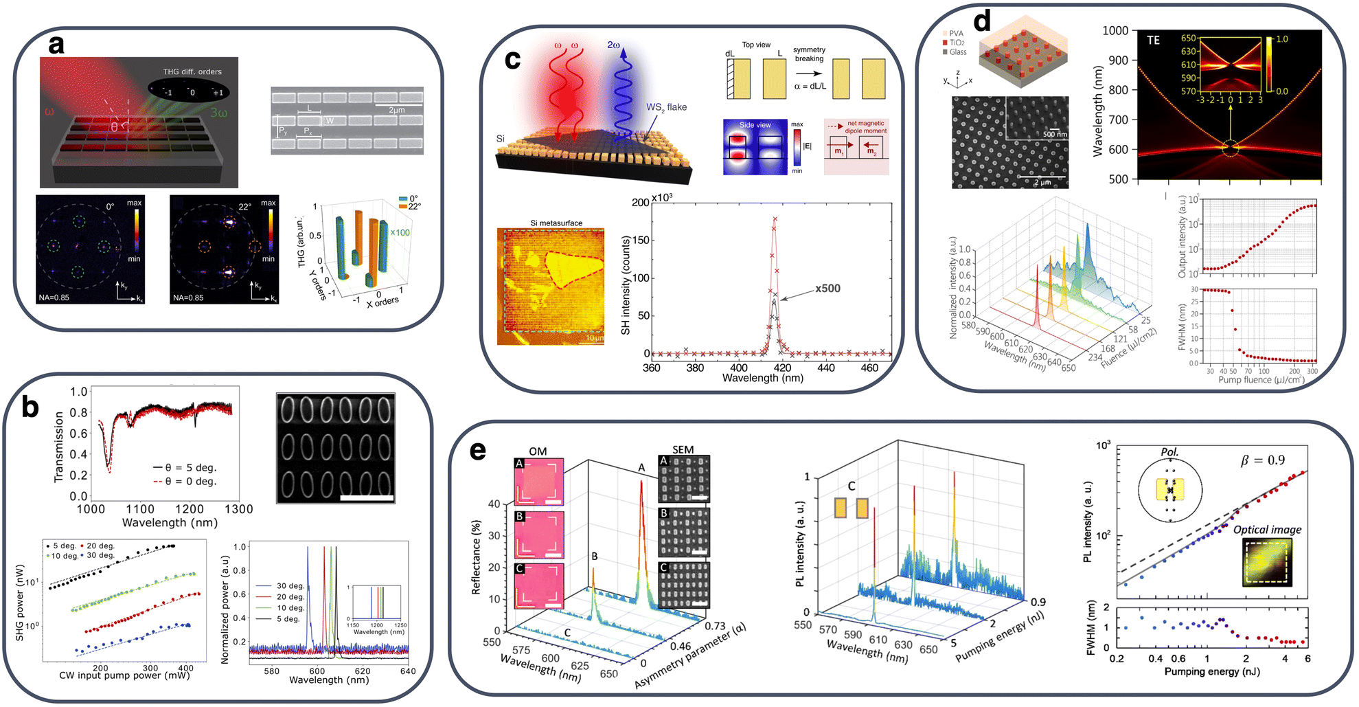 | ||
| Fig. 2 (a) Nonlinear wavefront control through third harmonic generation in qBIC Si metasurfaces. Adapted with permission from ref. 66. Copyright 2021 American Chemical Society. (b) GaP metasurface supporting qBIC resonances for enhanced continuous-wave second harmonic generation. Adapted with permission from ref. 42. Copyright 2020 American Chemical Society. (c) Strong light-matter interaction in WS2 monolayers coupled with qBIC resonances for enhanced second harmonic generation. Adapted with permission from ref. 30. Copyright 2020 American Chemical Society. (d) Low-threshold, directional lasing from organic dye coatings on a TiO2 metasurface supporting qBIC resonances in the visible range. Adapted with permission from ref. 50. Copyright 2021, Wiley-VCH. (e) Silicon nitride metasurfaces with lattice resonant qBIC for low-threshold lasing from rhodamine 6G as the gain material. Reprinted with permission from ref. 48. Copyright 2021, Wiley-VCH. | ||
Being centrosymmetric, Si is not suitable for second harmonic generation (SHG), even though SHG can be exceptionally observed in qBIC Si metasurfaces, stemming from symmetry-breaking-induced surface nonlinearity.29 Instead, SHG has been intensely investigated in III–V semiconductor qBIC metasurfaces. A proof-of-concept experimental demonstration employed a qBIC metasurface composed of GaAs/AlGaAs/AlGaO asymmetric cuboids and achieved a SHG efficiency 6 × 10⁻⁶ or 1000-fold increase with respect to a similar metasurface with a bright magnetic dipole resonance. The 11 nm linewidth of the 130 fs pump laser pulses was not matched to the qBIC resonance linewidth of 2 nm, which decreased the efficiency of the process. Anthur et al.42 employed a GaP tilted ellipsoid qBIC metasurface, measuring a high efficiency of 4 × 10⁻⁵ at a low pump intensity of 10 MW cm−2 in pulsed operation, as well as an efficiency of 2 × 10⁻⁷ under a continuous-wave (CW) intensity of 1 kW cm−2, reaching a SHG signal power around 70 nW for 360 mW of input pump power. Fig. 2(b) shows a SEM photo of the fabricated metasurface and the progressive enhancement of SHG for smaller tilt angles of the ellipsoids, which lead to higher Q-factors of the qBIC resonance. SHG was also demonstrated in a GaP-on-sapphire asymmetric bar qBIC metasurface with an experimental Q∼ 100.77
Theoretically, much higher SHG efficiencies are predicted, as in the case of a proposed LiNbO3 tilted ellipsoid qBIC metasurface assuming the realistic value of Q ∼ 8 × 10⁴, for which a 4.9 × 10⁻³ efficiency at Ip = 3.3 kW cm−2 was calculated.78 Metasurface engineering can also provide additional functionalities; Mobini et al.79 theoretically proposed a bianisotropic qBIC metasurface where the asymmetry was introduced by partially etching holes in AlGaAs nanodisks. This generates a mismatch in the multipole distribution of the resonator fields and phase profile between backward and forward illumination, which leads to around four order of magnitude ratio of the SHG signal power for opposite illumination.
Although Si metasurfaces are not suitable for SHG, they can be used as the tool to provide local field enhancement and boost the SHG efficiency in adjacent 2D sheets of TMD materials. To maximize this effect, the near-field profile should provide adequate overlap with the TMD layer, namely strong enhancement of the in-plane electric field components at the metasurface/TMD interface. Various experimental works have successfully demonstrated this potential. Lochner et al.45 demonstrated an SHG efficiency above 10−9 for pump power in the range of a few mW in a qBIC Si metasurface coupled with a monolayer of MoS2. The SHG signal was enhanced 35 times with respect to a non-patterned Si slab of the same thickness. Higher metasurface-induced enhancement was shown for an asymmetric bar qBIC metasurface coupled with a WS2 monolayer (1140 times).30Fig. 2(c) shows the structure and the strong field confinement of the qBIC resonant mode at the Si cuboid/WS2 flake interface, which enhances the SHG efficiency. Finally, a 9400-fold improvement was demonstrated in a strongly qBIC resonant (Q > 8000) asymmetric Si cuboid metasurface coupled with a few layer GaSe.37
HHG has been thus far the main, but not single, focus in qBIC metasurface-enhanced nonlinear optics. In a recent experimental work, Hu et al.80 demonstrated qBIC-induced 17-fold enhancement of broadband THz generation in a LiNbO3 on top of which a metasurface of symmetry-broken silica cuboids was patterned. This approach exploits the excellent non-linear properties of LiNbO3 while avoiding its non-trivial etching by patterning the metasurface in an additional low-index dielectric layer. The intensity of the THz signal was comparable to thin standard ZnTe emitters without limitation on the pump wavelength and it was successfully applied to conduct THz time-domain spectroscopic measurements.
2.3 Light emission and lasing
The subwavelength resonator dimensions and the high Q-factors of qBIC dielectric metasurfaces also make them ideal candidates for light emission platforms, as the low mode volume/strong resonances lead to a high Purcell factor. Although these features are shared by nanolasers based on single nanoresonators, in the latter case the low emission volume, output power, and nondirectional emission limit their application. In contrast, qBIC metasurfaces offer a scalably high emission volume and, by appropriate engineering, highly directional radiation.The enhancement of light emission in qBIC metasurfaces can be readily demonstrated in the context of photoluminescence (PL) measurements. Yuan et al.81 studied an embedded with Ge quantum dots (QD) Si-on-insulator (SOI) metasurface with slightly asymmetric holes, pumped by a diode laser at 532 nm. A 1000-fold PL enhancement with respect to a nonpatterned reference sample was observed, stemming from the near-field coupling of individual resonator oscillations in the metasurface. The emitted light inherited the polarization-properties of the qBIC modes, thus highlighting the connection between the qBIC mode properties and the far-field emitted radiation. A similar level of PL enhancement was demonstrated in a Si metasurface with symmetry-broken nanorods.36 The spontaneous emission from embedded Ge QDs was enhanced and outcoupled by the qBIC effect showing a narrow linewidth, up to Q = 1946 among the various qBIC modes, and directional emission. Again, it was shown that by controlling the position of the defect hole in the nanorods, which may lead to qBIC mode overlap, the emission pattern can be adjusted. Emission pattern control was also demonstrated through dispersion engineering in a GaAs metasurface with symmetry-broken nanocuboids and a single layer of epitaxially grown InAs QDs. The PL emission featured a linewidth of 3 nm and its brightness was enhanced by more than two orders of magnitude with respect to the nonpatterned reference, whereas the presence of the metasurface also significantly reduced the PL far-field divergence.82 In particular, the emission pattern depended strongly on the qBIC modal dispersion, with flat dispersion leading to intense spot-like with parabolic-type to ring-shaped radiation. In a more fundamental from the physics standpoint experiment, qBIC symmetry-broken metasurfaces were shown to strongly enhance the radiative recombination and thus PL of G-centers in crystalline Si, achieving a ∼40 times PL enhancement with zero threshold at cryogenic temperatures.83
In parallel, significant effort has been directed to the development of BIC lasers, as they represent versatile beam sources key to numerous applications, such as optical trapping, quantum computing, near-field spectroscopy and sensing, and topological photonics.84 The first optically pumped BIC laser operating at room temperature was demonstrated in 2017, using a suspended membrane of InGaAsP multiple QD supporting a robust A-BIC inside the gain spectrum.20 By employing a 12 ns pulsed laser pump at 1064 nm, lasing was observed at near-IR telecom wavelengths with a threshold power (power density) of 56 μW (140 mW mm−2) and down to a metasurface size of only 8 × 8 unit cells. A proof-of-concept directional BIC laser was shortly after investigated based on a GaAs nanopillar array on a fused SiO2 substrate embedded in a spin-on-glass, working at 77° K to avoid surface recombination in GaAs, which severely limits its gain at room temperature.40 The GaAs nanopillar was symmetric and resonating with a vertical dipole inhibiting in-plane radiation. To open a radiation channel, the periodicity of the metasurface was increased along one axis in order to allow for a diffractive channel.85 The BIC laser was pumped with 200 fs pulses at 780 nm and emitted narrowband (0.3 nm) radiation at 830 nm with a lasing threshold ∼14 μJ cm−2. Lasing occurred only at the specific angle of 3 °C, which corresponds to the crossing point of the leaky channels with the kx axis in the emission plane, thus demonstrating its highly directive nature.
A more versatile approach is based on the decoupling of the gain medium from the qBIC dielectric metasurface, such that the properties of the two can be independently tailored to meet a target application. Wu et al.49 studied optically pumped lasing from a colloidal film of CdSe/CdZnS core–shell nanoplatelets placed on top of a TiO2 nanocylinder metasurface supporting magnetic dipole and quadrupole BIC modes. Pumping was achieved by 200 fs pulses at 530 nm and lasing was observed above the threshold of 36 μJ cm−2 at ∼650 nm with a very narrow linewidth Q > 2590. Very interestingly, lasing was observed even though the symmetry of the metasurface was not broken, which in the case of an infinite structure would inhibit any radiation outcoupling. However, the finite size of the metasurface introduced a certain wavevector spread, as previously discussed, which translated in an emission with a small angular width around the normal direction. In the particular case of the investigated TiO2 metasurface the lasing intensity was maximum at 0.8° with respect to the normal. BIC lasing in a nanopillar TiO2 metasurface was also demonstrated using a solution of rhodamine 101 in poly(vinyl alcohol) as the gain medium. The qBIC was engineered by merging electric and magnetic dipoles close to the Rayleigh anomaly and lasing was observed at ∼614 nm with a threshold of 40 μJ cm−2, as demonstrated in Fig. 2(d).50 Furthermore, rhodamine 6G in dimethyl sulfoxide was used as the gain medium over a qBIC metasurface of asymmetric Si3N4 bars supporting a pair of antiphase surface lattice resonances. The BIC laser had a low threshold of ∼1.25 nJ and a spontaneous emission coupling factor β value of ∼0.9 at room temperature, as outlined in Fig. 2(e).48
BIC lasers allow for advanced functionalities owing to the particular physical properties that govern BIC modes. For instance, as already mentioned, BIC modes are topologically protected, manifesting as vortex centers in the polarization directions of far-field radiation.65 By exploiting such winding topologies of BIC resonances, the generation of optical vortices (OV) was demonstrated in photonic crystal slabs, featuring ring-like profiles in momentum space and thus behaving as quasi-Bessel beams with diffraction-resistant behaviour.86 Building on this concept, Huang et al.87 developed a lead bromide perovskite (MAPbBr3) metasurface with an array of circular holes capable of OV beam lasing, measuring emitted beams with the characteristic doughnut shape with a far-field angle of θ = 2°. More importantly, it was shown that by using a two-beam pump, lasing can be switched between OV to a linearly polarized beam with picosecond switching times and record-low energy consumption, paving the way for new applications in topological and quantum photonics.
Pushing the performance of BIC lasers to the extreme, Hwang et al.38 exploited the concept of merging BIC and the associated increase in the obtainable Q-factors thanks to the reduced dispersion of the qBIC mode. An InGaAsP free-standing membrane was patterned with a square nanohole lattice and its periodicity was optimized to work in the merging-BIC regime. The finite sample accommodated 40 × 40 unit cells and it was pumped by a 980 nm pulsed laser diode. Lasing was observed at the threshold peak power (density) of ∼340 μW (∼14.7 μW μm−2), which is by far lower than a previous demonstration of BIC nanolasers. The laser emitted at ∼1600 nm with an ultrahigh Q-factor of at least 7300, as the measurement was resolution limited, and a measured decay time of <138 ps, which is fast enough for high-speed modulation.
2.4 Refractometry and biosensing
The main performance metrics of micro- and nano-fluidic resonant refractometric sensors that ultimately determine their detection limit are their sensitivity S = Δλres/Δna, where λres and na are the resonant wavelength and analyte refractive index, respectively, and the figure of merit (FoM) defined as FoM = S/FWHM, where FWHM is the full-width at half maximum of the resonant mode linewidth. Although S can reach very high values in plasmonic sensors, the associated ohmic losses inherently limit the achievable Q-factor, and hence the FoM, as well as introduce heating, which can be detrimental in sensing biological materials. The ultrahigh achievable Q-factors together with the absence of Joule heating, an easy free-space coupling probing scheme, and planar geometry typically patterned with a single lithographic step, highlight the suitability of all-dielectric qBIC metasurfaces as the resonant probing mechanism in emerging refractometric and biological sensors.These favorable traits were demonstrated in one of the first studies on qBIC-metasurface sensing, which employed a Si3N4 metasurface supporting A-BICs in both the near-IR and the visible spectrum.46 The metasurface was integrated in a polydimethylsiloxane (PDMS) microfluidic chamber for the introduction of the analyte over a large sensing area. The sensor exhibited a very high performance (S = 178 nm RIU−1, Q = 2000, FoM = 445) and thanks to the strong near-field confinement and absence of heating it was also able to detect ultralow-molecular-weight molecules. Moreover, operation with an A-BIC mode increased the sensor's robustness to slight misalignments of the probing beam. Following this demonstration, it was shown that here there is much space for optimization in the proposed qBIC-SiN sensing platform towards much larger S by reducing the refractive index contrast between substrate and analyte at the expense of lower linearity and the larger required analyte volumes.47 Thanks to the strong field confinement, high Q-factors and absence of local heating, this A-BIC-SiN metasurface platform was also shown to enhance biosensing-relevant spectroscopic tools, such as surface-enhanced Raman and fluorescence spectroscopy. This was demonstrated by measuring fluorescence and Raman scattering signals from rhodamine-6G and the Raman analyte crystal violate, respectively, with more than a 1000-fold increase in signal intensity with respect to the reference nonpatterned Si3N4 slab,88 as shown in Fig. 3(a).
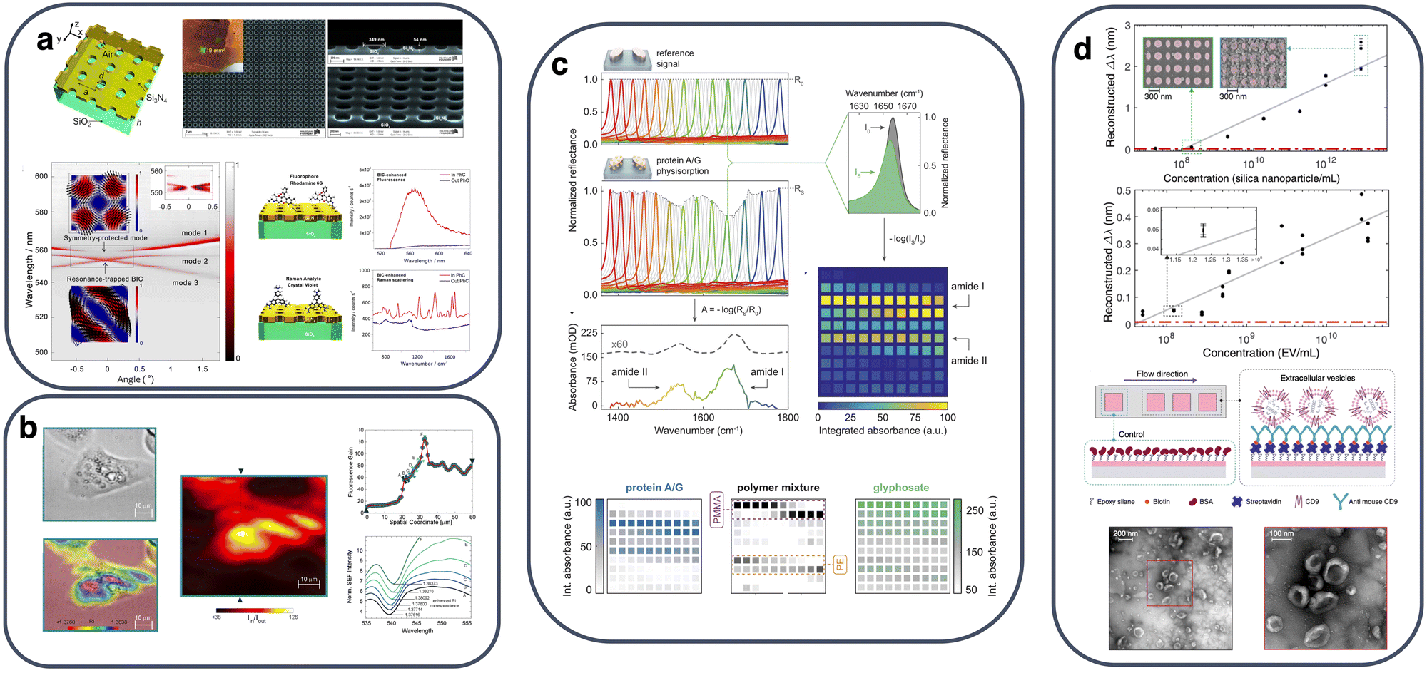 | ||
| Fig. 3 All-dielectric qBIC metasurfaces for refractometry and biosensing: (a) surface-enhanced fluorescence and Raman spectroscopy in qBIC-resonant Si nitride metasurfaces. Adapted with permission from ref. 88. Copyright 2018 American Chemical Society. (b) Hyperspectral refractometric imaging by combining SER and refractometric sensing by Fano interference of qBIC and fluorescence emission. Adapted with permission from ref. 18. Copyright 2020 American Chemical Society. (c) Mid-infrared molecular absorption reconstruction based on imaging through spectrally modulated pixelated qBIC-resonant metasurfaces. Reprinted with permission from ref. 51. Copyright 2018, American Association for the Advancement of Science. (d) Single-wavelength imaging biosensing in pixelated qBIC dielectric metasurfaces coupled with a microfluidic system for the real-time monitoring of extracellular vesicles.89 | ||
In other approaches, Wang et al.90 exploited a SOI nanodisk metasurface with an embedded PDMS probing chamber for both bulk refractometry and cancer biomarker (ErbB2) detection upon functionalizing the metasurface. Thanks to the large interaction of the near electric field of the exploited resonant BIC mode a high sensitivity of 720 nm RIU−1 was measured at ∼1.55 μm. The metasurface maintained its symmetry and it was probed by changing the angle of incidence of the input beam for a maximum measured Q = 270 at an angle of 1°. In terms of biomarker sensing, the metasurface featured a sensitivity of 2 nm nM−1 and a limit of detection of 0.7 ng mL−1, demonstrating the capacity of integrating the proposed CMOS-compatible metasurfaces in lab-on-chip components for biosensing and diagnosis. In a similar approach, a SOI metasurface of the titled nanoellipsoids functionalized for the detection of the biotoxin microcystin-LR (MC-LR) yielded a bulk sensitivity S = 788 nm RIU−1, measured Q ∼ 170 (FoM ∼ 100) and a very low detection limit for MC-LC of 0.002 ng mL−1.91 Label-free biosensing of DNA was demonstrated by functionalizing an A-BIC-SiN metasurface, detecting a concentration of 20 mol μm−2 paving the way for a single-molecule regime.92 Moreover, Wang et al.93 introduced a new type of Si-on-glass qBIC metasurface composed of asymmetric crescent-shapes meta-atoms, experimentally measuring a bulk sensitivity of 326 nm RIU−1 for a Q ∼ 120, as well as biomolecular layer sensing of streptavidin at sub-nM concentrations after biotin functionalization of the metasurface. In another recent experimental study of an asymmetric Si nanopillar qBIC metasurface bulk sensitivity and FoM values of 608 nm RIU−1 and 46 were demonstrated.94 Finally, Chen et al.95 proposed a qBIC metasurface composed of chiral TiO2 nanoposts patterned on a gold film, exploiting an A-BIC stemming from the destructive interference of a narrowband toroidal dipole mode and a surface lattice resonance. Simultaneous refractometric and chiral sensing was demonstrated, with S = 80.6 nm RIU−1 (FoM = 80.6) and a 59-fold enhancement of the circular dichroism signal, which enables integrated molar chiral sensing for enantiomer-specific analysis.
In the aforementioned approaches, sensing was performed at a single-pixel level, meaning that the optical beam probed the entire metasurface and provided information on the refractive index of the bulk overlayer or molecular layers captured to the metasurface by means of functionalization. However, the large sensing area offered by metasurfaces readily enables more advanced imaging functionalities. Romano et al.18 combined surface-enhanced fluorescence in a dye-covered A-BIC-SiN metasurface with qBIC resonances in a dual-mechanism correlative hyperspectral imaging platform where the peak resonant wavelength shift due to the refractive index variation was converted in a more sensitive readout based on photoemission intensity. This approach enabled the recording of a surface-enhanced correlative refractometric map with resolution in the order of 10−5 RIU within fL-scale sampling volumes. The system was successfully applied for mapping the spatially variant surface refractive index of live cells grown on the metasurface in microscopy configuration, as demonstrated in the results presented in Fig. 3(b).
Tittl et al.51 introduced a pixelated qBIC metasurface based on the Si tilted ellipsoid archetypal design, resonating in the mid-IR with an average Q ∼ 200. The structure was scaled 25 times, such that it sampled the target spectral range from 1350 to 1750 cm−1 at a resolution of 4 cm−1. When covered with a protein monolayer, this CMOS-compatible, multi-pixel qBIC metasurface chip provided an absorption map with a single measurement and without the need for complex instrumentation, based on which the absorption spectrum of the sample molecule is retrieved, as shown in the individual spectra and spectral maps of Fig. 3(c). By employing advanced recognition algorithms, the technique also allows for measuring the relative ratios in multi-substance samples.
Further expanding the concept, the same group demonstrated hyperspectral imaging for the massive parallel sensing of trace biomolecules or 2D materials.44 The sensor array can operate either with a high-resolution tunable source in order to generate a datacube whose post-processing yields the resonance shift map across the sampling area or by employing a modulated metasurface chip (demonstrated by a fabricated sensor of 275 × 275 pixels) and recording only intensity measurements, which are then decoded in pseudo-spectra. Digital sensing of mouse-derived immunoglobulin solutions was demonstrated with an extremely low concentration level of less than 3 mol μm−2, as well as single-layer graphene mapping over an area of 3.3 mm2. As a next step, single-wavelength biosensing imaging with spectral shift reconstruction was combined with microfluidic monitoring in an advanced sensing platform based on a qBIC metasurface of Si broken-symmetry dimer nanodisks, whose main aspects are summarized in Fig. 3(d). The resulting optofluidic chip was coupled to a CMOS camera collecting data over a large field of view. The sensing performance of the device was demonstrated in the real-time measurements of extracellular vesicles binding from down to 204 fM solutions, enabling detection of on average 0.41 nanoparticle μm−2.89
2.5 Other qBIC-enhanced metasurface functionalities
The fundamental difference between qBICs and bright resonances in dielectric metasurfaces is their asymptotically infinite radiative lifetime under symmetry protection in SP-BIC and radiation channel cancellation in A-BIC, and not in terms of their multipole nature and resonant fields. Therefore, qBICs can be employed in a variety of wave resonant phenomena, as a means to push their operation towards narrow bandwidths. A distinctive example of this approach is the coupling of qBIC physics with Huygens' metasurfaces in order to achieve highly-dispersive transmission-phase modulation over a 2π range with near-unity transmittance.96 A tilted-ellipsoid metasurface was engineered such that two qBIC resonances with matched Q-factors but opposite mode parities spectrally overlap, thus satisfying the Huygens' condition in a controllably small bandwidth and, hence, high effective group index. The concept was also experimentally demonstrated with a Q-factor around 75, as demonstrated in Fig. 4(a).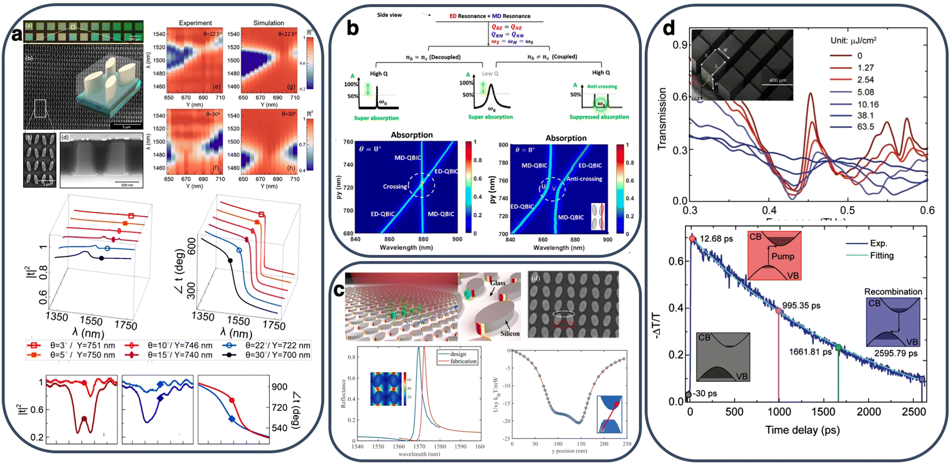 | ||
| Fig. 4 (a) Huygens' metasurface for phase control with adjustable narrowband operation based on the coupling of electric and magnetic qBIC. Adapted with permission from ref. 96. Copyright 2018 American Chemical Society. (b) Super- and suppressed narrowband absorption in critically-coupled metasurfaces supporting electric and magnetic dipole qBIC. The operation mode is controlled by the index contrast between substrate and background medium. Adapted with permission from ref. 97. Copyright 2020 American Chemical Society. (c) All-dielectric nanotweezers by leveraging trapping sites in the electromagnetic hot spots of qBIC-resonant Si metasurfaces. Adapted with permission from ref. 39. Copyright 2021 American Chemical Society. (d) Tunable terahertz qBIC dielectric metasurface through optically pumped carrier photogeneration in high-resistivity Si. Adapted with permission from ref. 53. Copyright 2019, Wiley-VCH. | ||
Using the tilted-ellipsoid metasurface paradigm, Tian et al.97 theoretically proposed a narrowband critical absorber, where two degenerate CC qBIC resonances with opposite symmetry account for 100% absorbance within a narrow spectral band (Q ∼ 640). Furthermore, it was shown that when operating at high-Q regime, an index asymmetry between the substrate and overlayer leads to suppressed absorption due to the anti-crossing of the two qBIC modes, as described in Fig. 4(b). Control by means of qBIC resonances of the CC bandwidth was also proposed in graphene-coupled qBIC metasurfaces, by matching the radiative rate of a MD qBIC resonance with the dissipative loss rate in graphene. The absorption bandwidth can be tuned over two orders of magnitude (∼1–100 nm) by adjusting the asymmetry factor of the proposed perturbed Si nanodisk metasurface and the Fermi level and number of graphene layers.98 In the same context, Yu et al. theoretically demonstrated that narrowband critical absorption can also occur in systems with non-orthogonal resonant modes through breaking of parity-time symmetry and engineering the system such that the coupling-induced mode splitting is suppressed.99 This approach provides larger degrees of freedom in terms of the mode losses as demonstrated in the example of a qBIC metasurface composed of tilted Si–Ge–Si ellipsoids. Another way to achieve high-Q superabsorption in all-dielectric systems is by employing a qBIC metasurface as a dispersive metamirror, which enhances the absorption at the thin film, as recently demonstrated in ref. 100. The metamirror consisted in a silicon tilted-ellipsoid metasurface supporting an electric qBIC mode and it was separated from a weakly absorbing Ge film by a silica quarter-wavelength spacer that induced coupling between the qBIC and Fabry–Perot resonant modes. An absorptance of 66.5% with Q = 282 was experimentally demonstrated at λ = 1242.3 nm.
In a different context, qBIC resonances were applied to control the bandwidth of the metasurface chiral response. By judiciously arranging tilted dielectric bars, it was shown that maximum artificial chirality can be achieved in a controllably narrow spectrum, where only one circular polarization is transmitted and without any polarization conversion. The concept is scalable and it was experimentally demonstrated in the microwave range.101 Similar chiral effects were theoretically investigated in SP-qBIC metasurfaces employing other planar geometries with broken in-plane inversion and mirror symmetry.102
Furthermore, an asymmetric nanobar qBIC metasurface was theoretically proposed as a means to enhance the Goos–Hänchen (GH) shift, which results from the phase variation over the angle of incidence in metasurfaces illuminated by a lightbeam with sufficient beam waist.103 By employing a MD-qBIC resonance, the asymmetry factor of the metasurface was translated into the resulting GH shift, demonstrating values above three orders of magnitude of wavelength, easily detectable at the reflection peak.
Finally, the tilted ellipsoid qBIC metasurface was also proposed as a nanotweezers platform for optically trapping nanoparticles, where the enhanced near-field among the ellipsoids leads to strong optical gradient forces, with negligible heating.39 Interestingly, it was shown that particle trapping can improve the resonant mode confinement in a positive feedback scheme, which enhances the trapping process. Experimentally measured Q-factor and field enhancement values of 2000 and 140, respectively, demonstrated the feasibility of the proposed application, as summarized in Fig. 4(c).
2.6 Dynamically tunable qBIC dielectric metasurfaces
Boosting metasurfaces with tunable functionalities has constantly been a key goal in view of the engineering of novel devices such as modulators, beam steerers, and adaptive metalenses, to name but a few. Following the rapidly expanding research in static qBIC dielectric metasurfaces, various approaches towards dynamically tunable components have started to be explored, leveraging the know-how in consolidated techniques employed in tunable/reconfigurable electromagnetic devices.One such approach relies on the free carrier generation in semiconductors, which modifies both their refractive index and loss coefficient through the free carrier dispersion effect. Terahertz HR-Si metasurfaces provide an ideal platform as HR-Si shows extremely low absorption losses, which can be modulated by carrier photogeneration through optical pumping, e.g. to dynamically control CC and modulate the metasurface transmittance.104 Han et al.53 experimentally measured Q-factors in the order of 250 in qBIC HR-Si. Resonance damping was dynamically controlled by increasing the intensity of the optical pump, achieving saturation at a low fluence of 10.16 μJ cm−2. The relaxation time of the metasurface was 2.6 ns, as shown in Fig. 4(d), which enables sub-GHz modulation. Similarly, Fan et al.52 investigated a THz qBIC metasurface of suspended interconnected HR-Si disks with a maximum Q = 8700 bound by nonradiative losses, showing that carrier-induced absorption is the dominant effect and saturating the qBIC resonance at moderate estimated doping values of ∼1015 using a photodoping power of 100 mW at 980 nm.
In the telecom relevant near-IR spectrum, electro-optical phase modulation was theoretical proposed in a metasurface of Si nanoellipsoids in a connected zigzag configuration with multijunction p–n structures that allow for multigate biasing. The metasurface is designed to operate at the Huygens' regime, where the carrier accumulation in the multijunction scheme allows for phase-only tuning of 240° at an average transmittance of 77% by a weak electro-refraction index modulation of 4 × 10⁻³ thanks to the strong qBIC resonances. Dynamic polarization control and tunable pulse compression and expansion were studied as enabled applications.105
Tunable phase modulation in Huygens' qBIC metasurfaces was also theoretically proposed recently by employing an overlayer of nematic liquid crystal (LC).106 Thanks to their inherent large optical anisotropy and electro-optic response, as well as the mature display and LC-on-Si technology, LC has been demonstrated as a versatile tunable medium in a large number of metadevices for applications where millisecond switching times are acceptable.107–109 A tilted-ellipsoid qBIC metasurface was considered in contact with a LC overlayer between two indium-tin-oxide electrodes for the application of bias voltage. Phase-only tuning was calculated in the full 2π range with a tuning bandwidth of around 3.5 nm, limited by the different shifting rates of the ED and MD qBIC resonances as a function of the anisotropic index tensor components. In a different approach, tunable notch filtering over 20 nm around 1.55 μm independent of the Q-factor was theoretically demonstrated in a Si nanocuboid metasurface supporting a delocalized qBIC resonance coupled with a planar LC cell in the overlayer.33
Other approaches for tunable qBIC dielectric metasurfaces have been proposed employing a variety of materials with tunable optical properties. Mikheeva et al.110 investigated an asymmetric bar qBIC metasurface made of photosensitive chalcogenide glass (CG) As2S3. Upon illumination, the CG refractive index showed a maximum index variation of 0.08 achievable at a pump fluence of 20 J cm−2, which resulted in the experimental shift of the qBIC resonance (Q ∼ 110) by 12 nm around 780 nm. Ge2Sb2Te5, another phase-change CG, was proposed theoretically to induce tunability in a qBIC metasurface, as a thin layer on top of the constituent Si asymmetric nanodisks. Switchable transmittance modulation was investigated, which can be applied in reconfigurable imaging.111 Furthermore, the electro-optical tuning of graphene's Fermi level was theoretically shown to tune the coupling between asymmetric Si split rings and a graphene layer, achieving 81% modulation depth in transmittance by exploiting the CC condition as the off-state.112 Magneto-optic tuning was proposed in a metasurface operating at the Brewster qBIC regime at specified angles of incidence, where the switchable excitation of the qBIC mode is controlled by reversing the applied magnetic field direction, as demonstrated theoretically in a Bi:YIG nanodisk metasurface.113 Finally, GHz electro-optical modulation was recently experimentally demonstrated by combining qBIC dielectric metasurfaces and the Si-organic-hybrid (SOH) platform, which has been extensively used for electro-optical modulation in integrated Si photonics. The qBIC resonance had a narrow linewidth (Q = 550 at λres = 1594 nm) and significant field overlap with the electro-optical polymer, thus achieving tuning of Δλres = 11 nm at a 3 dB modulation speed of 5 GHz.114
3 Recent advances in gradient all-dielectric metasurfaces
Gradient (or graded) metasurfaces for wavefront manipulation are composed of dissimilar meta-atoms, appropriately arranged in order to provide a purposeful spatial modulation of the phase delay supplied by the metasurface. This phase delay can be exploited for a broad range of wavefront manipulation operations, such as beam steering (linear spatial phase profile), beam focusing and splitting, general wavefront transformation (e.g. plane-wave to Bessel beam), and in- and out-coupling to surfaces states, to name just a few. As a result, they have an enormous practical application perspective in the important fields of communications, imaging and holography. Conventional versions of steering and focusing metasurfaces can be thought of as the flat, ultrathin counterparts of blazed gratings and Fresnel lenses, respectively. A notable difference is that in resonant metasurfaces the required phase is not being accumulated via propagation inside a bulk dielectric medium of variable thickness, but, rather, by controlling the phase delay supplied by the resonant meta-atom via shifting its resonant frequency with respect to the operating wavelength. In addition, metasurfaces are composed of discrete entities (meta-atoms) and thus lead to a discretized local phase profile. As long as the lattice constant is deeply subwavelength and the spatial phase profile finely discretized, the metasurface still behaves as a homogenizable medium and the underlying structure does not impact the response. Note, however, that the discrete nature is ultimately necessarily associated with spatial dispersion.All-dielectric versions of gradient metasurfaces are being investigated for the entire electromagnetic spectrum, ranging from microwave frequencies (e.g. using ceramic materials), all the way to infrared (e.g. using silicon) and visible frequencies (e.g. using TiO2). They are particularly important in higher frequencies (from the infrared to the visible), where they can offer reduced resistive loss compared to metallic counterparts. They have been predominantly implemented by exploiting geometry-dependent Mie resonances of dielectric particles. A broad range of particle shapes has been examined including disks,115 disks with a partially etched center hole (bianisotropic response),116 rods,117 C-shapes,118etc.
3.1 Evolution of gradient metasurface theory
Gradient metasurfaces witnessed a surge of research activity, following the formulation of the generalized Snell's laws of reflection and refraction, modified to include phase jumps imposed by a metasurface at the interface between bulk media.131 A phase discontinuity of a linear spatial profile amounts to an additional (constant) parallel wavevector contribution, leading to “anomalous reflection” (i.e., deviating from the specular reflection/refraction of Snell's law). The similarities with standard blazed grating theory have been discussed.132The prescription of a linear phase profile for anomalous reflection is based on a ray-optics approach; it has been also termed the “phase-shift approach”.10 It was soon realized that this approach has certain limitations. For large deflection angles, the diffraction efficiency decreases as the input and output impedance cannot be concomitantly matched.133 Moreover, deviating from the designated input angle has been shown to result in power coupling to other diffraction orders, also limiting the efficiency.134 Regarding practical design methodologies, it is frequently assumed that neighboring meta-atoms are only slightly dissimilar and almost uncoupled (acting as independent “secondary” sources with different phase shifts). Thus, each unit of the gradient metasurface is specified by considering a uniform periodic expansion and a look-up table is constructed to be used for implementing any arbitrary phase profile. However, in reality there can be strong near-field and far-field coupling, limiting the success of the design process in terms of the resulting performance, especially when a strong spatial modulation along the metasurface is required. One workaround for these practical difficulties is to start from a ray-optics prescription as the initial state/prediction of the design and subsequently perform numerical optimization.135
A different approach, frequently termed the “surface impedance approach”,10 determines the required electric and magnetic surface conductivities (or impedances) along the metasurface for performing a specific steering (or other wavefront manipulation) operation by stipulating the desired fields in the two semi-infinite spaces and applying the boundary conditions.10,136 It has been shown that for perfect beam deflection to a specific angle without any spurious diffraction in reflection or transmission (including the specular direction), the exact solution requires surface conductivities with locally active regions (or, equivalently, spatial dispersion), which are impractical to implement.133,137,138 The local reflection/transmission coefficient can exceed unity amplitude and the associated phase profile strongly deviates from being linear, especially for large deflection angles.138 By allowing for some controllable coupling to other diffraction orders, e.g., allowing some specular reflection, more practical surface conductivity prescriptions can be obtained, such as “passive-lossless” and “passive-lossy” designs.10,136,138 The characteristic example of the passive-lossless implementation leads to a tangent spatial modulation of the surface conductivities along the metasurface. The period of the tangent modulation is λ/(sinθout − sinθin) and depends on the operating wavelength. This conductivity profile can be recovered by the ray optics (or phase shift) approach, revealing a connection between the two methods.139
In recent years, significant effort has been devoted to addressing the limitations of the early versions of gradient metasurfaces. These include the (i) limited efficiency for large deflection angles, (ii) the practical complexity of designing and fabricating deeply-subwavelength and tightly-confining meta-atoms, especially for higher frequencies, and (iii) the inherently narrowband operation of resonant implementations. Some of the proposed approaches are discussed in the following sections, along with physical mechanisms for obtaining a tunable response.
3.2 Metagratings
Metagratings were proposed as a means of lifting some of the limitations of conventional gradient metasurfaces, namely, the limited efficiency for large deflection angles and the practical complexity of a dense meta-atom array required for a finely-discretized phase profile. They were first presented by Radi et al.145 and the underlying theory was further established shortly after.146,147 Instead of discretizing the phase profile, metagratings rely on the standard grating principle of periodically arranging (identical) scatterers at a distance greater than the operating wavelength. As such, they can open several diffraction channels and diffract incident radiation to different directions depending on the diffraction order. In contrast to conventional gratings, the inclusions are elaborate meta-atom scatterers with engineered radiation patterns. Metagratings use the scattering properties of the individual scatterers to nullify scattering towards the unwanted (propagating) diffraction orders and allow beam deflection towards one (the desired) diffraction order/deflection angle. In general, bianisotropic scatterers are needed to cancel out more than one direction. The concept was initially illustrated with metallic omega particles; however, it is naturally suited to dielectric structures and high frequencies, where metasurface periodicities typically cannot be deeply subwavelength and the available resolution in fabrication becomes more restrictive.Following the spirit of the metagrating concept, various dielectric metasurfaces appeared shortly in the literature for improving efficiency at higher deflection angles and relaxing size constraints. The designs were mostly based on multi-resonant and/or multi-part scatterers, periodically arranged at a super-wavelength distance. For example, in ref. 143 two dissimilar dielectric-rod particles are placed in a dimer configuration; the rod pair is periodically extended to form a metagrating. Incidence takes place on a plane that includes the rods' axes, i.e., the rods are positioned parallel to the optical axis. Rod pairs are also exploited in ref. 117 and 148, but their axes are perpendicular to the plane of incidence. In ref. 149 dissimilar dielectric (silicon) spheres are placed in a dimer configuration. Other rectangular shapes140 or even free-form geometries have also been proposed using topology optimization and inverse design.141 In most cases, the ability of exciting and coupling between different electric and magnetic dipole modes, as well as their higher-order multipoles,117,140,143 is the underlying physical mechanism that provides the required degrees of freedom for engineering the radiation pattern of the meta-atom scatterer.
Representative works on all-dielectric metagratings are compiled in Fig. 5, focusing on experimentally-verified designs. Fig. 5(a) depicts a silicon metasurface for operation at mid-infrared frequencies (6.5 μm).140 The metagrating pattern was carved in the 2.7 μm-thick device layer of a silicon wafer using HBr plasma dry etching. It was shown that a two-part, bianisotropic meta-molecule supporting four resonances of the appropriate symmetry can effectively channel the output radiation into a single selected diffraction order (the “+1”), while suppressing all other transmission/reflection radiation channels. Highly efficient light-bending for large deflection angles has been demonstrated: above 90% efficiency has been reported experimentally for a deflection angle of 45° and up to 85° via simulations. Freeform geometries have also been proposed with the help of inverse design and adjoint optimization [Fig. 5(b)].141 In a physically similar manner to Fig. 5(a), multiple modes need to be supported within the unit cell to allow for shaping the radiation pattern and promoting a single diffraction order among the six available (considering both transmission and reflection). Diffraction efficiencies above 80% for a deflection angle of 75° have been experimentally reported for both TE and TM polarizations at near-infrared wavelengths (∼1000 and ∼1300 nm). Besides beam deflection, beam splitting has been also demonstrated. Other dielectric materials have been also used for different frequency regimes, such as titanium dioxide for visible wavelengths (∼500 nm) [Fig. 5(c)].142 Two variants of asymmetric meta-atoms have been exploited for light-bending at ∼55° and ∼80° with efficiencies reaching ∼90% and ∼50%, respectively. More specifically, a two rod dimer was considered in the former case [upper panel in Fig. 5(c)], and a “fish-shape” design formed by the intersection of a ring and a triangle in the latter [lower panel in Fig. 5(c)].
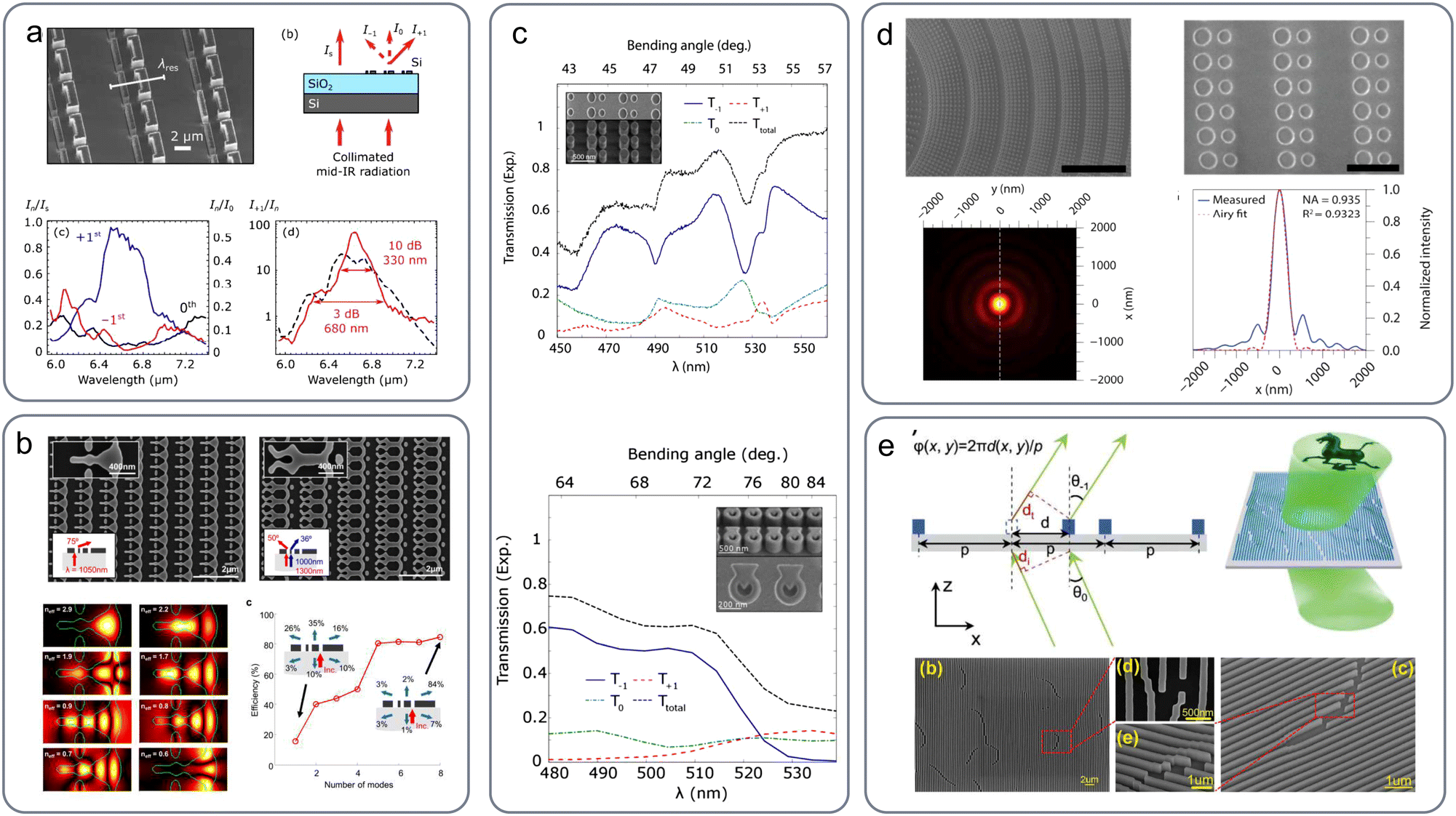 | ||
| Fig. 5 Dielectric implementations of metagratings. (a) Silicon-based metagrating for high-angle light bending at mid-infrared frequencies (6.5 μm).140 A two-part bianisotropic metamolecule supporting four resonances is proposed to selectively promote only one of the available radiation channels. Adapted with permission from ref. 140. Copyright 2018, American Chemical Society. (b) Silicon-based metagrating for light bending and beam splitting at near-infrared frequencies.141 A freeform geometry has been proposed based on inverse design and adjoint optimization. Adapted with permission from ref. 141. Copyright 2017, American Chemical Society. (c) Titanium dioxide metagrating for high-angle light bending at visible wavelengths (∼500 nm).142 Adapted with permission from ref. 142. Copyright 2017, American Chemical Society. (d) Spatially-modulated metagrating for a metalens with near-unity numerical aperture, enabled by the ability to efficiently bend light at high angles.143 The material is amorphous silicon and the operation wavelength is 715 nm. Adapted with permission from ref. 143. Copyright 2018, American Chemical Society. (e) SiNx-based metagrating with a spatially-modulated period for aribtrary wavefront manipulation in the visible region.144 Adapted with permission from ref. 144. Copyright 2020, Royal Society of Chemistry. | ||
By varying the period of the metagrating along the metasurface, i.e., extending the metagrating concept to non-uniform metasurfaces, the available output angles can be spatially varied and arbitrary wavefront manipulation can be achieved. This principle has been exploited for constructing a metalens with near-unity numerical aperture [Fig. 5(d)],143 enabled by the ability to efficiently bend light at angles as large as 82°. The proposed metalens is operating at a wavelength of 715 nm and possesses a subwavelength thickness of ∼λ/3. In order to fabricate the lens, thin films of amorphous silicon were deposited on fused silica substrates via chemical vapor deposition and subsequently patterned using electron beam lithography. Note that the lens design is based on a hybrid combination of the metagrating concept (for outer parts requiring large deflection angles) and the conventional “phase-shift approach” for inner parts. When small deflection angles are required out of the first diffraction order, large grating periods are needed resulting in the opening of many diffraction channels and making it difficult in practice to suppress all but one. The same concept of a metagrating with a modulated period is exploited in ref. 144 for enabling arbitrary wavefront shaping and demonstrating a meta-hologram with a continuously modulated phase profile [Fig. 5(e)]. The meta-grating was fabricated on a 300 nm-thick SiNx film by using reactive ion etching.
3.3 Achromatic metasurfaces
Conventional gradient metasurfaces for beam deflection, as well as metagratings, are periodic structures. They are inherently diffractive elements, which promote a single diffraction order by virtue of e.g. the “blazing” principle, or by positioning nulls in the radiation pattern of the constituent meta-atom, respectively. Due to their diffractive nature, they cannot sustain the same output angle (or more generally their functionality) over a broad wavelength range, i.e., they are inherently narrowband. This can be easily seen by the fact that the periodicity of the required phase profile would have to be different for each operating wavelength, according to φ(r + D,ω) = φ(r,ω) + m2π → D = mλ/(sinθout − sinθin). Even in the case of metalenses for e.g. beam focusing, which do not exhibit a periodic phase profile, the temporal bandwidth is still limited. This is because flat metalenses base their operation on resonant phase delay, which is inherently dispersive. Since typically a strong resonance response is desired, the temporal bandwidth can be very limited. In contrast, classical bulk lenses rely on propagating phase accumulation inside a dielectric material of variable thickness; in the complete absence of material dispersion, this would lead to dispersionless operation. While the narrowband character is not a problem for academic examples of continuous-plane-wave scattering, it is rather restrictive for real-world signals, which necessarily have significant temporal (and spatial) bandwidth. As a result, a new generation of research on achromatic gradient metasurfaces has been recently established, aiming to increase their temporal bandwidth and render them more suited to practical applications.124,150–152,154–158 Fundamental limits for the bandwidth of achromatic metalenses have been discussed based on the time-bandwidth limit in any time-invariant system.159
Dielectric achromatic metasurfaces were first demonstrated in the context of beam steering, where it was realized that to achieve the same deflection angle for different wavelengths the metasurface can no longer be periodic.154 Initially, Aieta et al.154 demonstrated achromatic operation (same deflection angle) for three discrete wavelengths. Subsequent demonstrations focused on a continuous wavelength range.124,151,152 The main enabling factor for these demonstrations proved to be the ability to independently control the phase delay and group delay (its spectral derivative). In dielectric implementations, one popular approach towards achromatic wavefront manipulation is phase accumulation within vertical waveguide segments.124,150–152 The waveguide cross-sections are engineered in order to allow for covering a broad range of different phase and group delays. An additional degree of freedom that can help tune the phase and group delay separately is the exploitation of the PB phase;152 however, in such cases the operation is not independent of polarization.
Representative works on all-dielectric achromatic gradient metasurfaces are compiled in Fig. 6, focusing on experimentally-verified designs. Arbabi et al.150 proposed a metasurface made of dielectric nano-posts of square cross-section [Fig. 6(a)] that can offer control over the accumulated phase and its derivative. The nano-posts function as multi-mode waveguide segments; by varying the dimensions of the cross-section the dispersion of the different supported modes is tuned. Using this approach, they have demonstrated the ability to switch from beam steering with negative dispersion (characteristic of diffraction gratings) all the way to achromatic beam steering and beam steering with positive dispersion, if so desired. The posts (vertical waveguide segments) are made of amorphous silicon and they reside on top of a silicon dioxide substrate backed by an aluminum reflector to operate in reflection. Besides achromatic beam steering, a focusing mirror with corrected chromatic aberrations has been demonstrated, exhibiting a constant focal length in the wavelength range 1450–1600 nm.
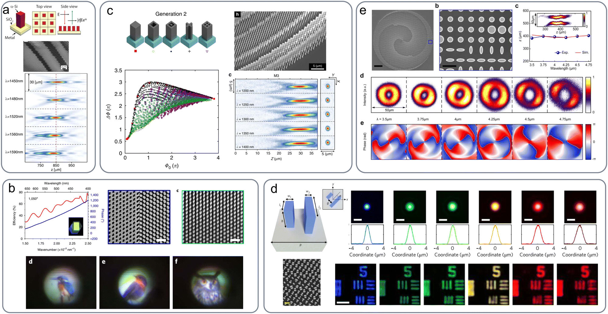 | ||
| Fig. 6 Dielectric implementations of achromatic metasurfaces. (a) Amorphous silicon nano-posts (vertical waveguide segments) of rectangular cross-sections supporting multiple waveguide modes for achromatic beam steering and focusing in reflection mode at near infrared frequencies.150 Adapted with permission from ref. 150. Copyright 2017, The Optical Society. (b) GaN nanopillars of rectangular cross-sections for achromatic metalenses at visible frequencies.151 The pillars and voids (complementary structures) are arranged in a hexagonal lattice and rotated to exploit the PB phase in addition to the accumulated propagation phase. Adapted with permission from ref. 151. Copyright 2018, Springer Nature Publishing Group. (c) Silicon nanopillars of various, elaborate cross-sections and varying dimensions enabling a broad range of achievable phase and group delays.124 An achromatic metalens (constant focal length) in the near infrared (λ= 1200–1650 nm) and efficiencies up to 50% have been experimentally demonstrated. Adapted from ref. 124. Copyright 2018, Author(s), licensed under a CC BY 4.0 License. (d) TiO2 coupled nano-fins for achromatic focusing at visible frequencies (470–670 nm).152 The nano-fin pair is rotated to exploit the PB phase in addition to the accumulated propagation phase. An efficiency of about 20% at 500 nm has been demonstrated. Adapted with permission from ref. 152. Copyright 2018, Springer Nature Publishing Group. (e) Elliptical silicon rods for achromatic focusing of an optical vortex beam at mid-infrared frequencies (3–5 μm).153 Adapted with permission from ref. 153. Copyright 2021, Wiley-VCH. | ||
An additional degree of freedom in engineering the phase and group delay independently can be offered by rotating meta-atoms which are rotationally asymmetric and utilizing the PB phase in addition to the accumulated propagation phase. Exploiting this strategy, Wang et al.151 demonstrated an achromatic metalens operating in the visible region [Fig. 6(b)]. Measurements with circularly polarized light have revealed an efficiency of 40% (power in focal spot over incident power on the metalens aperture) in transmission mode across the entire range 400–660 nm. For physical implementation of the metalens they have used GaN nanopillars of rectangular cross-section, as well as their complementary structures (rectangular voids). The meta-atoms were arranged in a hexagonal lattice and reside on top of a sapphire substrate.
The available span of achievable phase and group delay values can be significantly expanded if different, elaborate waveguide cross-sections are allowed. This has been successfully demonstrated by Shrestha et al.124 with silicon pillars of various cross-sections and dimensions [Fig. 6(c)]. The suggested pillar cross-sections all retain a four-fold rotational symmetry to allow for polarization-independent operation. A broad range of phase and group delay values is achieved leading to the experimental demonstration of a transmission-mode metalens with a near-constant focal length over the continuous near infrared frequency range λ = 1200–1650 nm exhibiting efficiencies up to 50%. The silicon on insulator material system used in this case is technologically favorable due to the CMOS electronics industry. Similar waveguide cross-sections but with TiO2 instead of Si have been utilized by Wang et al.160 for metalenses targeted at visible frequencies. In order to improve the process of expanding and selecting within the achievable span of phase and group delay, a backpropagation neural network and particle swarm optimization were utilized.
Coupled waveguides inside the unit cell is an alternative degree of freedom that can help enlarge the phase span. Chen et al.152 used coupled nano-fins of rectangular cross-section [Fig. 6(d)]. The operation principle is based both on propagating and PB phase (by rotating the fin pair). Achromatic imaging from 470 to 670 nm with an efficiency of about 20% at 500 nm has been demonstrated. Since the lens is targeted at the visible range, TiO2 was the material of choice for the nano-fins, exhibiting low loss and a high refractive index at these frequencies.
Besides the visible and near-infrared frequencies, interest exists for the mid-infrared range as well. Ou et al.153 demonstrated an all-silicon metalens for operation in the 3–5 μm wavelength range [Fig. 6(e)]. They have used silicon posts of a general elliptic cross-section and demonstrated focusing of optical vortex beams featuring a doughnut beam intensity and a helical phase distribution.
Alternative approaches towards providing large phase and group delays are also worth mentioning. In principle, one can avoid phase accumulation altogether and base the design solely on resonant phase delay.139 This approach can lead to even thinner metalens realizations (a finite thickness to allow for implementing magnetic polarizability without magnetic materials is still necessary). However, it necessitates the implementation of multiple resonances within the unit cell of both electric and magnetic nature.161,162 Each resonance can contribute a phase span of π and many of them are needed to provide the required phase delay. Through a specific combination of resonances, the individual dispersive phase delays of each resonance can merge into an aggregate, dispersionless phase profile (i.e., linear in frequency, resulting in a constant group delay) and enable achromatic operation. In a different approach, many electrically-polarizable metasurfaces are concatenated, distanced by spacers of non-negligible electric thickness, in order to provide dispersionless operation.155 This design approach capitalizes on standard filter design principles.
3.4 Tunability and reconfigurability
Gradient metasurfaces have started out as static structures with a fixed output (e.g. the deflection angle or the focal length). The ability to dynamically switch and/or continuously tune the characteristics of the output radiation is, naturally, a highly desirable goal. The most straightforward form of tuning is global tuning, i.e., controlling the unit cells of the gradient metasurface all at the same time with a single control signal. This can lead to on/off switching of the metasurface functionality, e.g., switching between anomalous and specular refraction.163 Additional freedom (and complexity) is introduced with local tuning, e.g., allowing each unit cell to be configured differently. This can lead to e.g. continuous tuning of the deflection angle120,165 and even allow for switching between different functionalities with the same structure (reconfigurability).128To enable tunability, materials with a strong response to an external control (bias voltage, temperature, static electric/magnetic field, etc.) are required. Such materials include liquid crystals (LCs),163,168–171 which constitute a mature technology even after the LCD-TFT displays. They are being used primarily for global tuning (see e.g. ref. 163). Local tuning is also realized at lower (e.g. microwave or THz) frequencies,169 but is challenging at optical frequencies, due to the subwavelength resolution required. Phase change materials167,172–175 are better suited to on–off switching rather than continuous tuning. They typically lead to a relatively slow response (μs timescale, or ns at best).176 Faster response times (ps timescale in principle) can be obtained via the electro-optic effect in semiconductors164 and transparent conducting oxides.129 Finally, carrier injection in semiconductors166 and micro-electromechanical systems (MEMS)165 have also been considered. Note that in microwave frequency ranges, lumped electronic elements and tunable integrated chips constitute a promising approach.177,178
In Fig. 7 we compile representative works on tunable gradient metasurfaces for beam deflection (as the fundamental wavefront manipulation functionality), mainly focusing on experimentally-demonstrated designs. Komar et al.163 proposed a gradient metasurface based on silicon-nanodisks forming a supercell of six disks of varying radius in order to enable beam steering at an angle of 12°. The metasurface is infiltrated with liquid crystals which can shift from the nematic to the isotropic state by varying the temperature [Fig. 7(a)]. When the LC is in the isotropic state, radiation is steered into the +1 diffraction order and light is transmitted into an angle of 12°. In the nematic state, the functionality is broken allowing for specular transmission. Apart from tunable beam steering, LCs have enabled switchable varifocal lenses based on amorphous Si170,179 or TiO2171,180 dielectric particles. The different focal lengths are accessed by electrically switching the orientation of the nematic LC molecules. Another application is in holographic metasurfaces with a switchable visual output, designed to act as gas sensors or temperature/pressure monitors.181,182
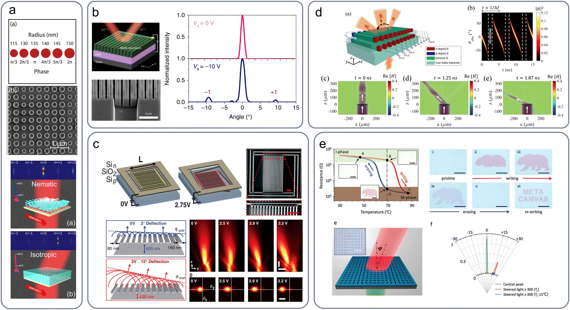 | ||
| Fig. 7 Physical mechanisms for switchable/tunable beam deflection with dielectric metasurfaces. (a) Silicon-nanodisk metasurfaces infiltrated with liquid crystals for switchable beam steering.163 A supercell of six disks is formed, designed to steer the beam into the +1 diffraction order (angle of 12°) when the LC is at the isotropic state. Adapted with permission from ref. 163. Copyright 2018, American Chemical Society. (b) Electro-optic effect in III–V multiple-quantum-wells (MQWs) for switchable beam steering between specular reflection and anomalous reflection to the ±1 diffraction orders (±10°).164 A bias voltage of −10 V is applied locally in order to produce a binary diffraction grating. Adapted from ref. 164. Copyright 2019, Author(s), licensed under a CC BY 4.0 License. (c) Tunable beam steering based on micro-electromechanical systems.165 A metasurface consisting of silicon nanowires is suspended above a reflective substrate; by controlling the distance from the substrate the reflection phase can be tuned and beam tilting up to 12° has been demonstrated (bias of 3.2 V). Adapted with permission from ref. 165. Copyright 2019, American Association for the Advancement of Science. (d) Carrier injection in silicon-nanobars configured into p–i–n junctions for tuning the refractive index of silicon (affecting the imaginary part as well).166 Tunable beam steering at the operating wavelength of 7 μm by varying the carrier density in the range of 1016–1019 cm−3. Adapted with permission from ref. 166. Copyright 2019, Wiley-VCH. (e) Reconfigurable (volatile) writing of a gradient metasurface pattern on a VO2 layer by exploiting the phase transition and switching local regions into the metallic phase. Reconfigurable beam steering at an angle of ∼20° is demonstrated.167 Adapted with permission from ref. 167. Copyright 2017, Wiley-VCH. | ||
In a different approach, the electro-optic effect in III–V multiple-quantum-wells (MQWs) can be exploited [Fig. 7(b)].164 A 1230 nm-thick MQW layer resides on a GaAs substrate followed by a distributed Bragg reflector to allow for operation in reflection; the MQWs were patterned into subwavelength elements supporting a hybrid Mie-guided mode resonance. The quantum-confined Stark effect is used to actively modulate the resonance properties, and can result in a reflection amplitude modulation of 270% and a reflection phase shift from 0° to ∼70°. The MQW metasurface is locally addressed in order to form a binary supercell; when the bias voltage reaches −10 V, radiation into the ±1 diffraction orders (angle of ±10°) emerges.
Holsteen et al.165 demonstrated tunable beam steering at visible frequencies using micro-electromechanical systems (MEMS) [Fig. 7(c)]. Their design, created in standard silicon-on-insulator technology, is based on a suspended metasurface made of silicon nanowires, which support Mie resonances. By controlling the height of the silicon wires (beams) through height deformation, the interaction between the particle resonances and the Fabry–Perot cavity that is formed vertically between the silicon-wire metasurface and the reflective substrate is tuned offering local control over the reflection phase. By applying low voltages, tunable beam steering between 2° (0 V) and 12° (3.2 V) is experimentally demonstrated. Moreover, they have also extended the supported functionality to beam focusing with a tunable focal length between 10 and 40 μm. The devices can operate dynamically with a speed reaching 1 MHz.
Carrier injection is another approach for tuning the refractive index and thus enabling tunability. Salary et al.166 theoretically proposed a doublet of silicon-nanobar arrays configured into p–i–n junctions [Fig. 7(d)]; each constituent layer is designed to support a high-quality-factor guided mode resonance. Carrier injection into the intrinsic region under forward bias allows for tuning the refractive index of silicon (affecting the imaginary part as well) and tuning the resonant properties. The required refractive index change of Δn = −0.42 in order to allow for complete control (0–2π) over the transmission phase can be obtained at the operating wavelength of 7 μm by varying the carrier density in the range 1016–1019 cm−3 (at the cost of carrier-induced optical loss). Fast dynamic modulation of the metasurface properties can enable spatiotemporal beam scanning and allow for frequency generation and mixing, degrees of freedom that otherwise require the exploitation of nonlinear materials.
Phase change materials can experience a phase transition in response to external stimuli. Transition metal oxides, such as VO2, can reversibly switch between a “dielectric” and a “metallic” phase. Utilizing this principle, Dong et al.167 proposed a reconfigurable (volatile) gradient metasurface, by writing the desired pattern on a VO2 layer via switching certain regions in the metallic phase [Fig. 7(e)]. This is achieved by a 532 nm continuous laser with a power around 1 mW in order to heat the respective regions (below 90 °C). The VO2 films were deposited onto double-side polished, undoped Si substrates via sputtering. Reconfigurable beam steering in transmission at an angle of ∼20° is experimentally demonstrated. Moreover, polarizer and concentric ring grating structures were realized. Besides transition metal oxides, chalcogen-based alloys such as the ternary germanium-antimony-tellurium (GST) compound Ge2Sb2Te5, have been also used for realizing tunable metasurfaces.183,184 Such compounds undergo an amorphous-to-crystalline (structural) transition and are prime candidates for non-volatile operation. In ref. 185, Chu et al. propose an anomalous reflection metasurface that can steer the output beam in a different direction by switching some of the GST rods comprising the supercell from the amorphous to the crystalline state. They show switching from a reflection angle of 0° to −20° and −40° at 1550 nm.
4 Conclusion and outlook
The performance of BIC metasurface components is expected to be boosted through the improvement of fabrication techniques and the exploitation of concepts such as ultralow-dispersion or merging BICs for record-high experimentally achievable Q-factors. This breakthrough can push the conversion efficiency in BIC nonlinear metasurfaces to unprecedented values and provide a powerful tool for the development of novel applications based on non-linear and/or exciton physics in emerging 2D materials. More exotic non-linear effects can also be enabled, such as the theoretically predicted strongly enhanced generation of photon pairs with narrow frequency spectra and sharp angular correlations through spontaneous parametric down-conversion in BIC metasurfaces towards a new paradigm of miniaturized quantum light sources.186,187Although the basic principles of lasing from BIC metasurfaces have been established, demonstrating versatile control of the emission angle, polarization, and even topological charge of the emitted lightbeam, their true potential is yet to be unveiled as the thus far proof-of-concept demonstrations were based on optical pumping. Electrically pumped BIC metasurface lasers will provide the missing element towards their integration as light sources in numerous photonic architectures. In addition, BIC dielectric metasurfaces can be used to enhance the efficiency of other light generation mechanisms, such as BIC-enhanced Smith-Purcell radiation by coupling free electrons to qBIC states.188
Biosensing has perhaps reached the most advanced level of maturity among the various BIC metasurface-based applications, with very high FoM sensors demonstrated for both bulk and monolayer sensing at extremely low concentration levels. In addition, various imaging platforms have been successfully demonstrated based on coupled effects, such as surface-enhanced fluorescence and qBIC resonances, or by engineering CMOS-compatible chips with multipixel probes and powerful retrieval algorithms for reconstructing molecular absorbance, analyzing multi-substance samples, and mapping the properties of single-layer 2D materials. Further progress is expected to push the detection limits to record-low concentrations and provide integrated lab-on-chip architectures for parallel sensing, potentially also combined with nanoparticle trapping.
Moreover, as they are based on a general wave resonant phenomenon, BIC metasurfaces can in principle achieve the functionalities of their counterparts based on bright mode resonances. As such, it is envisaged that BIC metasurfaces can push the performance of standard metasurface response types, such as manipulation of a propagating wave's amplitude, phase, polarization, beamshape, towards ultra-narrowband operation with extreme variations and strongly dispersive behaviour. This has already been demonstrated in BIC metasurface narrowband critical absorbers, phase modulation at the Hyugens' regime, and artificially chiral metasurfaces.
Finally, integrating BIC dielectric metasurfaces with dynamically tunable media shows extreme potential, as several enabling technologies for electro-optic, mechanical, or all-optical are technologically mature, whereas tunability in BIC metasurfaces is still in its first steps of exploration. Carrier photogeneration in HR-Si THz metasurfaces, optical phase change in photosensitive CG near-IR metasurfaces and electro-optical transmission modulation in SOH BIC near-IR metasurfaces are a few already experimentally proven concepts for the development of novel tunable components operating in different parts of the electromagnetic spectrum. A promising degree of freedom to dynamically adjust the metasurface response is the mechanical tuning of its periodicity by employing a stretchable polymeric substrate as demonstrated in non-BIC dielectric metasurface examples.107 Carrier injection, the Pockels or Kerr effect and the use of LC or phase-change materials can complete the picture and significantly broaden the spectrum of BIC metasurface functionalities for the engineering of novel devices spanning a broad range of emerging applications.
Gradient metasurfaces are expected to further mature in the following years, by addressing the remaining performance issues and aligning with the limitations of large-scale fabrication techniques in order to offer compact, lightweight, and fabrication-friendly alternatives to conventional bulky optical components. The ability to efficiently bend light at near-grazing angles with metagratings has already allowed for designing metalenses with a record-high NA approaching unity.143 On a different front, achromatic metalenses based on vertical waveguide segments have shown the potential for impressive operation bandwidths with a constant focal length and minimal chromatic aberrations. Implementations at both infrared and visible frequencies have been demonstrated.124,152 In visible frequencies where the available refractive index contrast is weaker, more elaborate designs in order to further increase the efficiency and the bandwidth are desirable. Another worthy challenge concerns the ability to combine the attributes of high NA/large-angle bending and achromatic response in a single metalens implementation (being periodic structures, metagratings are inherently dispersive and, thus, narrowband).
The possibility to extend the temporal bandwidth of metasurfaces, despite their resonant nature, is highly desirable also in other functionalities besides wavefront manipulation. Characteristic examples are pulse delay without distortion162 (frequently termed “true time delay”) and pulse compression or broadening for dispersion compensation or chirped pulse amplification, respectively.189 More generally, the ability to arbitrarily control the shape and chirp (instantaneous frequency) of a short input pulse, depends on being able to freely engineer the spectral profile of the phase (and amplitude) of the reflection/transmission coefficient over a broad frequency range. The angular (spatial) bandwidth of metasurfaces also remains a point of interest, since their discrete nature is ultimately necessarily accompanied by spatial dispersion.
In terms of dynamic tunability, all-dielectric gradient metasurfaces have a long way to go towards meeting the ultimate goal of locally addressed and continuously tunable reconfigurable structures that can provide multiple functionalities with high efficiency and are able to quickly switch between (short response time). To this end, different materials/approaches may be necessitated for different frequency regimes (microwave, THz, optical frequencies). In addition, the possibility of fast temporal modulation opens up a window into general spatiotemporal metasurfaces190 and enables a broad range of additional possibilities.191,192 For example, it allows combining wavefront manipulation operations with frequency generation and mixing, offering an interesting alternative to nonlinear metasurfaces. Furthermore, temporal modulation can break time-reversal and therefore realize nonreciprocal wave propagation.
Author contributions
Both authors planned the work, drafted and proof-read the manuscript. O. T. and D. C. Z. prepared the sections on gradient and strongly resonant metasurfaces, respectively.Conflicts of interest
There are no conflicts to declare.Acknowledgements
This work was supported by the Hellenic Foundation for Research and Innovation (H.F.R.I.) under the “2nd Call for H.F.R.I. Research Projects to support Post-doctoral Researchers” (Project No. 916, PHOTOSURF). The authors acknowledge the COST Action Symat (CA18223), supported by COST (European Cooperation in Science and Technology), and are grateful for the support received from the CNR Short Term Mobility program 2021. D. C. Z. acknowledges the support from the CNR-FAPESP biennial (2022–2023) bilateral project StReAM “Strongly Resonant All-dielectric Metasurfaces based on quasi-dark and toroidal modes”.Notes and references
- C. M. Soukoulis and M. Wegener, Nat. Photonics, 2011, 5, 523–530 CrossRef CAS.
- S. B. Glybovski, S. A. Tretyakov, P. A. Belov, Y. S. Kivshar and C. R. Simovski, Phys. Rep., 2016, 634, 1–72 CrossRef CAS.
- H.-T. Chen, A. J. Taylor and N. Yu, Rep. Prog. Phys., 2016, 79, 076401 CrossRef PubMed.
- Q. He, S. Sun and L. Zhou, et al. , Research, 2019, 2019, 1849272 CAS.
- S. Sun, Q. He, J. Hao, S. Xiao and L. Zhou, Adv. Opt. Photonics, 2019, 11, 380–479 CrossRef.
- A. E. Minovich, A. E. Miroshnichenko, A. Y. Bykov, T. V. Murzina, D. N. Neshev and Y. S. Kivshar, Laser Photonics Rev., 2015, 9, 195–213 CrossRef.
- K. Koshelev, A. Bogdanov and Y. Kivshar, Sci. Bull., 2019, 64, 836–842 CrossRef.
- S. I. Azzam and A. V. Kildishev, Adv. Opt. Mater., 2020, 9, 2001469 CrossRef.
- M.-S. Hwang, K.-Y. Jeong, J.-P. So, K.-H. Kim and H.-G. Park, Commun. Phys., 2022, 5, 106 CrossRef.
- A. Epstein and G. V. Eleftheriades, J. Opt. Soc. Am. B, 2016, 33, A31–A50 CrossRef CAS.
- N. M. Estakhri and A. Alù, J. Opt. Soc. Am. B, 2016, 33, A21–A30 CrossRef CAS.
- A. C. Overvig, S. C. Malek, M. J. Carter, S. Shrestha and N. Yu, Phys. Rev. B, 2020, 102, 035434 CrossRef CAS.
- P. Yu, A. S. Kupriianov, V. Dmitriev and V. R. Tuz, J. Appl. Phys., 2019, 125, 143101 CrossRef.
- V. Dmitriev, D. Zografopoulos, S. D. Silva Santos and G. F. da Silva Barros, J. Phys. D: Appl. Phys., 2022, 55, 205104 CrossRef.
- J. F. Algorri, F. Dell'Olio, P. Roldán-Varona, L. Rodríguez-Cobo, J.-M. López-Higuera, J. Sánchez-Pena, V. Dmitriev and D. C. Zografopoulos, Opt. Express, 2022, 30, 4615–4630 CrossRef CAS PubMed.
- K. Koshelev, S. Lepeshov, M. Liu, A. Bogdanov and Y. Kivshar, Phys. Rev. Lett., 2018, 121, 193903 CrossRef PubMed.
- S. Murai, D. R. Abujetas, G. W. Castellanos, J. A. Sánchez-Gil, F. Zhang and J. G. Rivas, ACS Photonics, 2020, 7, 2204–2210 CrossRef CAS.
- S. Romano, M. Mangini, E. Penzo, S. Cabrini, A. C. D. Luca, I. Rendina, V. Mocella and G. Zito, ACS Nano, 2020, 14, 15417–15427 CrossRef PubMed.
- S. Han, P. Pitchappa, W. Wang, Y. K. Srivastava, M. V. Rybin and R. Singh, Adv. Opt. Mater., 2021, 9, 2002001 CrossRef CAS.
- A. Kodigala, T. Lepetit, Q. Gu, B. Bahari, Y. Fainman and B. Kanté, Nature, 2017, 541, 196–199 CrossRef CAS PubMed.
- A. I. Ovcharenko, C. Blanchard, J.-P. Hugonin and C. Sauvan, Phys. Rev. B, 2020, 101, 155303 CrossRef CAS.
- D. R. Abujetas, J. Olmos-Trigo and J. A. Sánchez-Gil, Adv. Opt. Mater., 2022, 2200301 CrossRef CAS.
- S. Li, C. Zhou, T. Liu and S. Xiao, Phys. Rev. A, 2019, 100, 063803 CrossRef CAS.
- Z. Sadrieva, K. Frizyuk, M. Petrov, Y. Kivshar and A. Bogdanov, Phys. Rev. B, 2019, 100, 115303 CrossRef CAS.
- Y. He, G. Guo, T. Feng, Y. Xu and A. E. Miroshnichenko, Phys. Rev. B, 2018, 98, 16112(R) Search PubMed.
- V. R. Tuz, P. Yu, V. Dmitriev and Y. S. Kivshar, Phys. Rev. Appl., 2020, 13, 044003 CrossRef CAS.
- D. C. Zografopoulos, J. F. Algorri, J. M. López-Higuera, H. E. Hernandez-Figueroa and V. Dmitriev, Sci. Rep., 2022, 12, 12975 CrossRef CAS PubMed.
- K. Koshelev, Y. Tang, K. Li, D.-Y. Choi, G. Li and Y. Kivshar, ACS Photonics, 2019, 6, 1639–1644 CrossRef CAS.
- Z. Liu, Y. Xu, Y. Lin, J. Xiang, T. Feng, Q. Cao, J. Li, S. Lan and J. Liu, Phys. Rev. Lett., 2019, 123, 253901 CrossRef CAS PubMed.
- N. Bernhardt, K. Koshelev, S. J. White, K. W. C. Meng, J. E. Fröch, S. Kim, T. T. Tran, D.-Y. Choi, Y. Kivshar and A. S. Solntsev, Nano Lett., 2020, 20, 5309–5314 CrossRef CAS PubMed.
- J. F. Algorri, F. Dell'Olio, P. Roldán-Varona, L. Rodríguez-Cobo, J. M. López-Higuera, J. M. Sánchez-Pena and D. C. Zografopoulos, Opt. Express, 2021, 29, 10374 CrossRef CAS PubMed.
- A. S. Kupriiannov, K. L. Domina, V. V. Khardikov, A. B. Evlyukhin and V. R. Tuz, Opt. Lett., 2020, 45, 1527–1531 CrossRef CAS PubMed.
- D. C. Zografopoulos and V. Dmitriev, J. Lightwave Technol., 2021, 39, 6985–6993 CAS.
- T. Christopoulos, O. Tsilipakos, G. Sinatkas and E. E. Kriezis, Opt. Express, 2019, 27, 14505–14522 CrossRef CAS PubMed.
- J. Jin, X. Yin, L. Ni, M. Soljačić, B. Zhen and C. Peng, Nature, 2019, 574, 501–504 CrossRef CAS PubMed.
- C. Cui, C. Zhou, S. Yuan, X. Qiu, L. Zhu, Y. Wang, Y. Li, J. Song, Q. Huang, Y. Wang, C. Zeng and J. Xia, ACS Photonics, 2018, 5, 4074–4080 CrossRef CAS.
- Z. Liu, J. Wang, B. Chen, Y. Wei, W. Liu and J. Liu, Nano Lett., 2021, 21, 7405–7410 CrossRef CAS PubMed.
- M.-S. Hwang, H.-C. Lee, K.-H. Kim, K.-Y. Jeong, S.-H. Kwon, K. Koshelev, Y. Kivshar and H.-G. Park, Nat. Commun., 2021, 12, 4135 CrossRef CAS PubMed.
- S. Yang, C. Hong, Y. Jiang and J. C. Ndukaife, ACS Photonics, 2021, 8, 1961–1971 CrossRef CAS.
- S. T. Ha, Y. H. Fu, N. K. Emani, Z. Pan, R. M. Bakker, R. Paniagua-Domínguez and A. I. Kuznetsov, Nat. Nanotechnol., 2018, 13, 1042–1047 CrossRef CAS PubMed.
- S. Campione, S. Liu, L. I. Basilio, L. K. Warne, W. L. Langston, T. S. Luk, J. R. Wendt, J. L. Reno, G. A. Keeler, I. Brener and M. B. Sinclair, ACS Photonics, 2016, 3, 2362–2367 CrossRef CAS.
- A. P. Anthur, H. Zhang, R. Paniagua-Dominguez, D. A. Kalashnikov, S. T. Ha, T. W. W. Maß, A. I. Kuznetsov and L. Krivitsky, Nano Lett., 2020, 20, 8745–8751 CrossRef CAS PubMed.
- P. P. Vabishchevich, S. Liu, M. B. Sinclair, G. A. Keeler, G. M. Peake and I. Brener, ACS Photonics, 2018, 5, 1685–1690 CrossRef CAS.
- F. Yesilkoy, E. R. Arvelo, Y. Jahani, M. Liu, A. Tittl, V. Cevher, Y. Kivshar and H. Altug, Nat. Photon., 2019, 13, 390–396 CrossRef CAS.
- F. J. F. Löchner, A. George, K. Koshelev, T. Bucher, E. Najafidehaghani, A. Fedotova, D.-Y. Choi, T. Pertsch, I. Staude, Y. Kivshar, A. Turchanin and F. Setzpfandt, ACS Photonics, 2020, 8, 218–227 CrossRef.
- S. Romano, G. Zito, S. Torino, G. Calafiore, E. Penzo, G. Coppola, S. Cabrini, I. Rendina and V. Mocella, Photon. Res., 2018, 6, 726–733 CrossRef CAS.
- S. Romano, G. Zito, S. N. L. Yépez, S. Cabrini, E. Penzo, G. Coppola, I. Rendina and V. Mocellaark, Opt. Express, 2019, 27, 18776 CrossRef CAS PubMed.
- J.-H. Yang, Z.-T. Huang, D. N. Maksimov, P. S. Pankin, I. V. Timofeev, K.-B. Hong, H. Li, J.-W. Chen, C.-Y. Hsu, Y.-Y. Liu, T.-C. Lu, T.-R. Lin, C.-S. Yang and K.-P. Chen, Laser Photon. Rev., 2021, 15, 2100118 CrossRef CAS.
- M. Wu, S. T. Ha, S. Shendre, E. G. Durmusoglu, W.-K. Koh, D. R. Abujetas, J. A. Sánchez-Gil, R. Paniagua-Domínguez, H. V. Demir and A. I. Kuznetsov, Nano Lett., 2020, 20, 6005–6011 CrossRef CAS PubMed.
- S. I. Azzam, K. Chaudhuri, A. Lagutchev, Z. Jacob, Y. L. Kim, V. M. Shalaev, A. Boltasseva and A. V. Kildishev, Las. Photon. Rev., 2021, 15, 2000411 CrossRef CAS.
- A. Tittl, A. Leitis, M. Liu, F. Yesilkoy, D.-Y. Choi, D. N. Neshev, Y. S. Kivshar and H. Altug, Science, 2018, 360, 1105–1109 CrossRef CAS PubMed.
- K. Fan, I. V. Shadrivov and W. J. Padilla, Optica, 2019, 6, 169–173 CrossRef CAS.
- S. Han, L. Cong, Y. K. Srivastava, B. Qiang, M. V. Rybin, A. Kumar, R. Jain, W. X. Lim, V. G. Achanta, S. S. Prabhu, Q. J. Wang, Y. S. Kivshar and R. Singh, Adv. Mater., 2019, 31, 1901921 CrossRef PubMed.
- A. S. Kupriianov, Y. Xu, A. Sayanskiy, V. Dmitriev, Y. S. Kivshar and V. R. Tuz, Phys. Rev. Appl., 2019, 12, 014024 CrossRef CAS.
- D. R. Abujetas, Á. Barreda, F. Moreno, A. Litman, J.-M. Geffrin and J. A. Sánchez-Gil, Laser Photonics Rev., 2020, 15, 2000263 CrossRef.
- D. C. Zografopoulos, J. F. Algorri, W. Fuscaldo, J. M. López-Higuera, R. Vergaz, J. M. Sánchez-Pena, I.-A. Karolos, R. Beccherelli, V. E. Tsioukas, T. V. Yioultsis and E. E. Kriezis, Adv. Opt. Mater., 2021, 9, 2002143 CrossRef CAS.
- Z. Chen, X. Yin, J. Jin, Z. Zheng, Z. Zhang, F. Wang, L. He, B. Zhen and C. Peng, Sci. Bull., 2022, 67, 359–366 CrossRef.
- D. C. Zografopoulos, A. Ferraro, J. F. Algorri, P. Martín-Mateos, B. García-Cámara, A. Moreno-Oyervides, V. Krozer, P. Acedo, R. Vergaz, J. M. Sánchez-Pena and R. Beccherelli, Adv. Opt. Mater., 2019, 7, 1900777 CrossRef CAS.
- J. Kühne, J. Wang, T. Weber, L. Kühner, S. A. Maier and A. Tittl, Nanophotonics, 2021, 10, 4305–4312 CrossRef.
- A. Taghizadeh and I.-S. Chung, Appl. Phys. Lett., 2017, 111, 031114 CrossRef.
- E. Yeganegi, A. Lagendijk, A. P. Mosk and W. L. Vos, Phys. Rev. B: Condens. Matter Mater. Phys., 2014, 89, 045123 CrossRef.
- M. S. Mohamed, Y. Lai, M. Minkov, V. Savona, A. Badolato and R. Houdré, ACS Photonics, 2018, 5, 4846–4853 CrossRef CAS.
- A. C. Overvig, S. Shrestha and N. Yu, Nanophotonics, 2018, 7, 1157–1168 CAS.
- C. W. Hsu, B. Zhen, J. Lee, S.-L. Chua, S. G. Johnson, J. D. Joannopoulos and M. Soljačić, Nature, 2013, 499, 188–191 CrossRef CAS PubMed.
- B. Zhen, C. W. Hsu, L. Lu, A. D. Stone and M. Soljačić, Phys. Rev. Lett., 2014, 113, 257401 CrossRef PubMed.
- K. I. Okhlopkov, A. Zilli, A. Tognazzi, D. Rocco, L. Fagiani, E. Mafakheri, M. Bollani, M. Finazzi, M. Celebrano, M. R. Shcherbakov, C. D. Angelis and A. A. Fedyanin, Nano Lett., 2021, 21, 10438–10445 CrossRef CAS PubMed.
- E. Almpanis and N. Papanikolaou, J. Appl. Phys., 2013, 114, 083106 CrossRef.
- L. Xu, K. Z. Kamali, L. Huang, M. Rahmani, A. Smirnov, R. Camacho-Morales, Y. Ma, G. Zhang, M. Woolley, D. Neshev and A. E. Miroshnichenko, Adv. Sci., 2019, 6, 1802119 CrossRef PubMed.
- G. Yang, S. U. Dev, M. S. Allen, J. W. Allen and H. Harutyunyan, Nano Lett., 2022, 22, 2001–2008 CrossRef PubMed.
- I. S. Sinev, K. Koshelev, Z. Liu, A. Rudenko, K. Ladutenko, A. Shcherbakov, Z. Sadrieva, M. Baranov, T. Itina, J. Liu, A. A. Bogdanov and Y. Kivshar, Nano Lett., 2021, 21, 8848–8855 CrossRef CAS PubMed.
- T. Ning, X. Li, Z. Zhang, Y. Huo, Q. Yue, L. Zhao and Y. Gao, Opt. Express, 2021, 29, 17286–17294 CrossRef CAS PubMed.
- G. Zograf, K. Koshelev, A. Zalogina, V. Korolev, R. Hollinger, D.-Y. Choi, M. Zuerch, C. Spielmann, B. Luther-Davies, D. Kartashov, S. V. Makarov, S. S. Kruk and Y. Kivshar, ACS Photonics, 2022, 9, 567–574 CrossRef CAS.
- M. Gandolfi, A. Tognazzi, D. Rocco, C. D. Angelis and L. Carletti, Phys. Rev. A, 2021, 104, 023524 CrossRef CAS.
- A. Theodosi, O. Tsilipakos, C. M. Soukoulis, E. N. Economou and M. Kafesaki, Opt. Express, 2022, 30, 460–472 CrossRef CAS PubMed.
- S. Xiao, M. Qin, J. Duan, F. Wu and T. Liu, Phys. Rev. B, 2022, 105, 195440 CrossRef CAS.
- L. Xu, D. A. Smirnova, R. Camacho-Morales, R. A. Aoni, K. Z. Kamali, M. Cai, C. Ying, Z. Zheng, A. E. Miroshnichenko, D. N. Neshev and M. Rahmani, New J. Phys., 2022, 24, 035002 CrossRef.
- D. Khmelevskaia, D. I. Markina, V. V. Fedorov, G. A. Ermolaev, A. V. Arsenin, V. S. Volkov, A. S. Goltaev, Y. M. Zadiranov, I. A. Tzibizov, A. P. Pushkarev, A. K. Samusev, A. A. Shcherbakov, P. A. Belov, I. S. Mukhin and S. V. Makarov, Appl. Phys. Lett., 2021, 118, 201101 CrossRef CAS.
- L. Kang, H. Bao and D. H. Werner, Opt. Lett., 2021, 46, 633 CrossRef PubMed.
- E. Mobini, R. Alaee, R. W. Boyd and K. Dolgaleva, ACS Photonics, 2021, 8, 3234–3240 CrossRef CAS.
- L. Hu, B. Wang, Y. Guo, S. Du, J. Chen, J. Li, C. Gu and L. Wang, Adv. Opt. Mater., 2022, 10, 2200193 CrossRef CAS.
- S. Yuan, X. Qiu, C. Cui, L. Zhu, Y. Wang, Y. Li, J. Song, Q. Huang and J. Xia, ACS Nano, 2017, 11, 10704–10711 CrossRef CAS PubMed.
- S. Liu, A. Vaskin, S. Addamane, B. Leung, M.-C. Tsai, Y. Yang, P. P. Vabishchevich, G. A. Keeler, G. Wang, X. He, Y. Kim, N. F. Hartmann, H. Htoon, S. K. Doorn, M. Zilk, T. Pertsch, G. Balakrishnan, M. B. Sinclair, I. Staude and I. Brener, Nano Lett., 2018, 18, 6906–6914 CrossRef CAS PubMed.
- L. Zhu, S. Yuan, C. Zeng and J. Xia, Adv. Opt. Mater., 2020, 8, 1901830 CrossRef CAS.
- R.-M. Ma and R. F. Oulton, Nat. Nanotechnol., 2019, 14, 12–22 CrossRef CAS PubMed.
- Z. F. Sadrieva, I. S. Sinev, K. L. Koshelev, A. Samusev, I. V. Iorsh, O. Takayama, R. Malureanu, A. A. Bogdanov and A. V. Lavrinenko, ACS Photonics, 2017, 4, 723–727 CrossRef CAS.
- B. Wang, W. Liu, M. Zhao, J. Wang, Y. Zhang, A. Chen, F. Guan, X. Liu, L. Shi and J. Zi, Nat. Photonics, 2020, 14, 623–628 CrossRef CAS.
- C. Huang, C. Zhang, S. Xiao, Y. Wang, Y. Fan, Y. Liu, N. Zhang, G. Qu, H. Ji, J. Han, L. Ge, Y. Kivshar and Q. Song, Science, 2020, 367, 1018–1021 CrossRef CAS PubMed.
- S. Romano, G. Zito, S. Managò, G. Calafiore, E. Penzo, S. Cabrini, A. C. D. Luca and V. Mocella, J. Phys. Chem. C, 2018, 122, 19738–19745 CrossRef CAS.
- Y. Jahani, E. R. Arvelo, F. Yesilkoy, K. Koshelev, C. Cianciaruso, M. D. Palma, Y. Kivshar and H. Altug, Nat. Commun., 2021, 12, 3246 CrossRef CAS PubMed.
- Y. Wang, M. A. Ali, E. K. Chow, L. Dong and M. Lu, Biosens. Bioelectron., 2018, 107, 224–229 CrossRef CAS PubMed.
- B. Ma, A. Ouyang, J. Zhong, P. A. Belov, R. K. Sinha, W. Qian, P. Ghosh and Q. Li, Electronics, 2021, 10, 1363 CrossRef CAS.
- G. Zito, G. Sanità, B. G. Alulema, S. N. L. Yépez, V. Lanzio, F. Riminucci, S. Cabrini, M. Moccia, C. Avitabile, A. Lamberti, V. Mocella, I. Rendina and S. Romano, Nanophotonics, 2021, 10, 4279–4287 CrossRef CAS.
- J. Wang, J. Kühne, T. Karamanos, C. Rockstuhl, S. A. Maier and A. Tittl, Adv. Funct. Mater., 2021, 31, 2104652 CrossRef CAS.
- H.-H. Hsiao, Y.-C. Hsu, A.-Y. Liu, J.-C. Hsieh and Y.-H. Lin, Adv. Opt. Mater., 2022, 2200812 CrossRef CAS.
- Y. Chen, C. Zhao, Y. Zhang and C. Wei Qiu, Nano Lett., 2020, 20, 8696–8703 CrossRef CAS PubMed.
- M. Liu and D.-Y. Choi, Nano Lett., 2018, 18, 8062–8069 CrossRef CAS PubMed.
- J. Tian, Q. Li, P. A. Belov, R. K. Sinha, W. Qian and M. Qiu, ACS Photonics, 2020, 7, 1436–1443 CrossRef CAS.
- X. Wang, J. Duan, W. Chen, C. Zhou, T. Liu and S. Xiao, Phys. Rev. B, 2020, 102, 155432 CrossRef CAS.
- J. Yu, B. Ma, A. Ouyang, P. Ghosh, H. Lao, A. Pattanayak, S. Kaur, M. Qiu, P. Belov and Q. Li, Optica, 2021, 8, 1290–1295 CrossRef.
- J. Yu, B. Ma, R. Qin, P. Ghosh, M. Qiu and Q. Li, ACS Photonics, 2022, 9, 3391–3397 CrossRef CAS.
- M. V. Gorkunov, A. A. Antonov, V. R. Tuz, A. S. Kupriianov and Y. S. Kivshar, Adv. Opt. Mater., 2021, 9, 2100797 CrossRef CAS.
- K.-H. Kim and J.-R. Kim, Adv. Opt. Mater., 2021, 9, 2101162 CrossRef CAS.
- Z. Zheng, Y. Zhu, J. Duan, M. Qin, F. Wu and S. Xiao, Opt. Express, 2021, 29, 29541 CrossRef CAS PubMed.
- X. Zhao, Y. Wang, J. Schalch, G. Duan, K. Cremin, J. Zhang, C. Chen, R. D. Averitt and X. Zhang, ACS Photonics, 2019, 6, 830–837 CrossRef CAS.
- M. M. Salary and H. Mosallaei, ACS Photonics, 2020, 7, 1813–1829 CrossRef CAS.
- Z. Yang, M. Liu, A. Komar, L. Xu and D. N. Neshev, Adv. Opt. Mater., 2021, 10, 2101893 CrossRef.
- R. Kowerdziej, A. Ferraro, D. C. Zografopoulos and R. Caputo, Adv. Opt. Mater., 2022, 10, 2200750 CrossRef CAS.
- B. Vasić, G. Isić, R. Beccherelli and D. C. Zografopoulos, IEEE J. Sel. Top. Quantum Electron., 2020, 26, 7701609 Search PubMed.
- B. Vasić, D. C. Zografopoulos, G. Isić, R. Beccherelli and R. Gajić, Nanotechnology, 2017, 28, 124002 CrossRef PubMed.
- E. Mikheeva, K. Koshelev, D.-Y. Choi, S. Kruk, J. Lumeau, R. Abdeddaim, I. Voznyuk, S. Enoch and Y. Kivshar, Opt. Express, 2019, 27, 33847 CrossRef CAS PubMed.
- C. Zhou, X. Qu, S. Xiao and M. Fan, Phys. Rev. Appl., 2020, 14, 044009 CrossRef CAS.
- T.-Y. Zeng, G.-D. Liu, L.-L. Wang and Q. Lin, Opt. Express, 2021, 29, 40177 CrossRef CAS PubMed.
- D. R. Abujetas, N. de Sousa, A. García-Martín, J. M. Llorens and J. A. Sánchez-Gil, Nanophotonics, 2021, 10, 4223–4232 CrossRef CAS.
- I.-C. Benea-Chelmus, S. Mason, M. L. Meretska, D. L. Elder, D. Kazakov, A. Shams-Ansari, L. R. Dalton and F. Capasso, Nat. Commun., 2022, 13, 3170 CrossRef CAS PubMed.
- M. Decker, I. Staude, M. Falkner, J. Dominguez, D. N. Neshev, I. Brener, T. Pertsch and Y. S. Kivshar, Adv. Opt. Mater., 2015, 3, 813–820 CrossRef CAS.
- V. Asadchy, M. Albooyeh and S. Tretyakov, J. Opt. Soc. Am. B, 2016, 33, A16–A20 CrossRef CAS.
- W. Liu and A. E. Miroshnichenko, ACS Photonics, 2017, 5, 1733–1741 CrossRef.
- A. Forouzmand and H. Mosallaei, Adv. Opt. Mater., 2017, 1700147 CrossRef.
- C. Pfeiffer and A. Grbic, Phys. Rev. Lett., 2013, 110, 197401 CrossRef PubMed.
- O. Tsilipakos, A. C. Tasolamprou, T. Koschny, M. Kafesaki, E. N. Economou and C. M. Soukoulis, Adv. Opt. Mater., 2018, 6, 1800633 CrossRef CAS PubMed.
- K. Achouri and O. J. F. Martin, 2021, arXiv:2103.10345.
- C. Gigli, Q. Li, P. Chavel, G. Leo, M. L. Brongersma and P. Lalanne, Laser Photonics Rev., 2021, 15, 2000448 CrossRef CAS.
- J. P. Balthasar Mueller, N. A. Rubin, R. C. Devlin, B. Groever and F. Capasso, Phys. Rev. Lett., 2017, 118, 113901 CrossRef CAS PubMed.
- S. Shrestha, A. C. Overvig, M. Lu, A. Stein and N. Yu, Light: Sci. Appl., 2018, 7, 85 CrossRef PubMed.
- J. Billuart, S. Héron, B. Loiseaux, C. Amra and M. Lequime, Opt. Express, 2021, 29, 32764 CrossRef CAS PubMed.
- A. McClung, M. Mansouree and A. Arbabi, Light: Sci. Appl., 2020, 9, 93 CrossRef CAS PubMed.
- J.-S. Park, S. Zhang, A. She, W. T. Chen, P. Lin, K. M. A. Yousef, J.-X. Cheng and F. Capasso, Nano Lett., 2019, 19, 8673–8682 CrossRef CAS PubMed.
- O. Tsilipakos, A. C. Tasolamprou, A. Pitilakis, F. Liu, X. Wang, M. S. Mirmoosa, D. C. Tzarouchis, S. Abadal, H. Taghvaee, C. Liaskos, A. Tsioliaridou, J. Georgiou, A. Cabellos-Aparicio, E. Alarcón, S. Ioannidis, A. Pitsillides, I. F. Akyildiz, N. V. Kantartzis, E. N. Economou, C. M. Soukoulis, M. Kafesaki and S. Tretyakov, Adv. Opt. Mater., 2020, 8, 2000783 CrossRef CAS.
- A. Forouzmand, M. Salary, G. K. Shirmanesh, R. Sokhoyan, H. A. Atwater and H. Mosallaei, Nanophotonics, 2019, 8, 415–427 CAS.
- J. Cheng, S. Inampudi, F. Fan, X. Wang, S. Chang and H. Mosallaei, Opt. Express, 2018, 26, 12547 CrossRef CAS PubMed.
- N. Yu, P. Genevet, M. A. Kats, F. Aieta, J.-P. Tetienne, F. Capasso and Z. Gaburro, Science, 2011, 334, 333–337 CrossRef CAS PubMed.
- S. Larouche and D. R. Smith, Opt. Lett., 2012, 37, 2391–2393 CrossRef PubMed.
- A. Daz-Rubio, V. S. Asadchy, A. Elsakka and S. A. Tretyakov, Sci. Adv., 2017, 3, e1602714 CrossRef PubMed.
- A. Epstein and G. V. Eleftheriades, Phys. Rev. B: Condens. Matter Mater. Phys., 2014, 90, 235127 CrossRef.
- F. Liu, O. Tsilipakos, A. Pitilakis, A. C. Tasolamprou, M. S. Mirmoosa, N. V. Kantartzis, D.-H. Kwon, J. Georgiou, K. Kossifos, M. A. Antoniades, M. Kafesaki, C. M. Soukoulis and S. A. Tretyakov, Phys. Rev. Appl., 2019, 11, 044024 CrossRef CAS.
- M. Selvanayagam and G. V. Eleftheriades, Opt. Express, 2013, 21, 14409–14429 CrossRef PubMed.
- A. Epstein and G. V. Eleftheriades, Phys. Rev. Lett., 2016, 117, 256103 CrossRef PubMed.
- N. M. Estakhri and A. Alù, Phys. Rev. X, 2016, 6, 041008 Search PubMed.
- O. Tsilipakos, M. Kafesaki, E. N. Economou, C. M. Soukoulis and T. Koschny, Adv. Opt. Mater., 2020, 8, 2000942 CrossRef CAS.
- Z. Fan, M. R. Shcherbakov, M. Allen, J. Allen, B. Wenner and G. Shvets, ACS Photonics, 2018, 5, 4303–4311 CrossRef CAS.
- D. Sell, J. Yang, S. Doshay, R. Yang and J. A. Fan, Nano Lett., 2017, 17, 3752–3757 CrossRef CAS PubMed.
- E. Khaidarov, H. Hao, R. Paniagua-Domínguez, Y. F. Yu, Y. H. Fu, V. Valuckas, S. L. K. Yap, Y. T. Toh, J. S. K. Ng and A. I. Kuznetsov, Nano Lett., 2017, 17, 6267–6272 CrossRef CAS PubMed.
- R. Paniagua-Domínguez, Y. F. Yu, E. Khaidarov, S. Choi, V. Leong, R. M. Bakker, X. Liang, Y. H. Fu, V. Valuckas, L. A. Krivitsky and A. I. Kuznetsov, Nano Lett., 2018, 18, 2124–2132 CrossRef PubMed.
- Z.-L. Deng, X. Ye, H.-Y. Qiu, Q.-A. Tu, T. Shi, Z.-P. Zhuang, Y. Cao, B.-O. Guan, N. Feng, G. P. Wang, P. Kapitanova, A. Alù, J.-W. Dong and X. Li, Nanoscale, 2020, 12, 20604–20609 RSC.
- Y. Ra’di, D. L. Sounas and A. Alù, Phys. Rev. Lett., 2017, 119, 067404 CrossRef PubMed.
- H. Chalabi, Y. Ra’di, D. L. Sounas and A. Alù, Phys. Rev. B, 2017, 96, 075432 CrossRef.
- A. Epstein and O. Rabinovich, Phys. Rev. Appl., 2017, 8, 054037 CrossRef.
- T.-J. Huang, L.-Z. Yin, J. Zhao and P.-K. Liu, Nanophotonics, 2021, 10, 2859–2873 CrossRef.
- E. Panagiotidis, E. Almpanis, N. Stefanou and N. Papanikolaou, J. Appl. Phys., 2020, 128, 093103 CrossRef CAS.
- E. Arbabi, A. Arbabi, S. M. Kamali, Y. Horie and A. Faraon, Optica, 2017, 4, 625–632 CrossRef.
- S. Wang, P. C. Wu, V.-C. Su, Y.-C. Lai, M.-K. Chen, H. Y. Kuo, B. H. Chen, Y. H. Chen, T.-T. Huang, J.-H. Wang, R.-M. Lin, C.-H. Kuan, T. Li, Z. Wang, S. Zhu and D. P. Tsai, Nat. Nanotechnol., 2018, 13, 227 CrossRef CAS PubMed.
- W. T. Chen, A. Y. Zhu, V. Sanjeev, M. Khorasaninejad, Z. Shi, E. Lee and F. Capasso, Nat. Nanotechnol., 2018, 13, 220–226 CrossRef CAS PubMed.
- K. Ou, F. Yu, G. Li, W. Wang, J. Chen, A. E. Miroshnichenko, L. Huang, T. Li, Z. Li, X. Chen and W. Lu, Laser Photonics Rev., 2021, 15, 2100020 CrossRef CAS.
- F. Aieta, M. A. Kats, P. Genevet and F. Capasso, Science, 2015, 347, 1342–1345 CrossRef CAS PubMed.
- S. M. A. M. H. Abadi, K. Ghaemi and N. Behdad, IEEE Trans. Antennas Propag., 2015, 63, 534–542 Search PubMed.
- S. Wang, P. C. Wu, V.-C. Su, Y.-C. Lai, C. Hung Chu, J.-W. Chen, S.-H. Lu, J. Chen, B. Xu, C.-H. Kuan, T. Li, S. Zhu and D. P. Tsai, Nat. Commun., 2017, 8, 187 CrossRef PubMed.
- A. A. Fathnan and D. A. Powell, Opt. Express, 2018, 26, 29440–29450 CrossRef PubMed.
- A. A. Fathnan, A. E. Olk and D. A. Powell, J. Phys. D: Appl. Phys., 2020, 53, 495304 CrossRef.
- F. Presutti and F. Monticone, Optica, 2020, 7, 624–631 CrossRef CAS.
- F. Wang, G. Geng, X. Wang, J. Li, Y. Bai, J. Li, Y. Wen, B. Li, J. Sun and J. Zhou, Adv. Opt. Mater., 2022, 10, 2101842 CrossRef CAS.
- O. Tsilipakos, T. Koschny and C. M. Soukoulis, ACS Photonics, 2018, 5, 1101–1107 CrossRef CAS PubMed.
- O. Tsilipakos, L. Zhang, M. Kafesaki, C. M. Soukoulis and T. Koschny, ACS Photonics, 2021, 8, 1649–1655 CrossRef CAS.
- A. Komar, R. Paniagua-Domínguez, A. Miroshnichenko, Y. F. Yu, Y. S. Kivshar, A. I. Kuznetsov and D. Neshev, ACS Photonics, 2018, 5, 1742–1748 CrossRef CAS.
- P. C. Wu, R. A. Pala, G. K. Shirmanesh, W.-H. Cheng, R. Sokhoyan, M. Grajower, M. Z. Alam, D. Lee and H. A. Atwater, Nat. Commun., 2019, 10, 3654 CrossRef PubMed.
- A. L. Holsteen, A. F. Cihan and M. L. Brongersma, Science, 2019, 365, 257–260 CrossRef CAS PubMed.
- M. M. Salary, S. Farazi and H. Mosallaei, Adv. Opt. Mater., 2019, 7, 1900843 CrossRef CAS.
- K. Dong, S. Hong, Y. Deng, H. Ma, J. Li, X. Wang, J. Yeo, L. Wang, S. Lou, K. B. Tom, K. Liu, Z. You, Y. Wei, C. P. Grigoropoulos, J. Yao and J. Wu, Adv. Mater., 2017, 30, 1703878 CrossRef PubMed.
- A. Komar, Z. Fang, J. Bohn, J. Sautter, M. Decker, A. Miroshnichenko, T. Pertsch, I. Brener, Y. S. Kivshar, I. Staude and D. N. Neshev, Appl. Phys. Lett., 2017, 110, 071109 CrossRef.
- M. Sazegar and R. Stevenson, 2020 IEEE International Symposium on Antennas and Propagation and North American Radio Science Meeting, 2020.
- M. Bosch, M. R. Shcherbakov, K. Won, H.-S. Lee, Y. Kim and G. Shvets, Nano Lett., 2021, 21, 3849–3856 CrossRef CAS PubMed.
- Y. Hu, X. Ou, T. Zeng, J. Lai, J. Zhang, X. Li, X. Luo, L. Li, F. Fan and H. Duan, Nano Lett., 2021, 21, 4554–4562 CrossRef CAS PubMed.
- C. H. Chu, M. L. Tseng, J. Chen, P. C. Wu, Y.-H. Chen, H.-C. Wang, T.-Y. Chen, W. T. Hsieh, H. J. Wu, G. Sun and D. P. Tsai, Laser Photonics Rev., 2016, 10, 986–994 CrossRef CAS.
- Q. Wang, E. T. F. Rogers, B. Gholipour, C.-M. Wang, G. Yuan, J. Teng and N. I. Zheludev, Nat. Photonics, 2015, 10, 60–65 CrossRef.
- F. Ding, S. Zhong and S. I. Bozhevolnyi, Adv. Opt. Mater., 2018, 6, 1701204 CrossRef.
- F. Ding, Y. Yang and S. I. Bozhevolnyi, Adv. Opt. Mater., 2019, 7, 1801709 CrossRef.
- G. Sinatkas, T. Christopoulos, O. Tsilipakos and E. E. Kriezis, J. Appl. Phys., 2021, 130, 010901 CrossRef CAS.
- A. Pitilakis, O. Tsilipakos, F. Liu, K. M. Kossifos, A. C. Tasolamprou, D.-H. Kwon, M. S. Mirmoosa, D. Manessis, N. V. Kantartzis, C. Liaskos, M. A. Antoniades, J. Georgiou, C. M. Soukoulis, M. Kafesaki and S. A. Tretyakov, IEEE Trans. Antennas Propag., 2021, 69, 1440–1454 Search PubMed.
- A. Pitilakis, M. Seckel, A. Tasolamprou, F. Liu, A. Deltsidis, D. Manessis, A. Ostmann, N. Kantartzis, C. Liaskos, C. Soukoulis, S. Tretyakov, M. Kafesaki and O. Tsilipakos, Phys. Rev. Appl., 2022, 17, 064060 CrossRef CAS.
- T. Badloe, I. Kim, Y. Kim, J. Kim and J. Rho, Adv. Sci., 2021, 8, 2102646 CrossRef PubMed.
- A. Lininger, A. Y. Zhu, J.-S. Park, G. Palermo, S. Chatterjee, J. Boyd, F. Capasso and G. Strangi, Proceedings of the National Academy of Sciences, 2020, 117, 20390–20396 CrossRef CAS PubMed.
- I. Kim, M. A. Ansari, M. Q. Mehmood, W.-S. Kim, J. Jang, M. Zubair, Y.-K. Kim and J. Rho, Adv. Mater., 2020, 32, 2004664 CrossRef CAS PubMed.
- I. Kim, W.-S. Kim, K. Kim, M. A. Ansari, M. Q. Mehmood, T. Badloe, Y. Kim, J. Gwak, H. Lee, Y.-K. Kim and J. Rho, Sci. Adv., 2021, 7, eabe9943 CrossRef CAS PubMed.
- Z. Xu, H. Luo, H. Zhu, Y. Hong, W. Shen, J. Ding, S. Kaur, P. Ghosh, M. Qiu and Q. Li, Nano Lett., 2021, 21, 5269–5276 CrossRef CAS PubMed.
- Y. Wang, P. Landreman, D. Schoen, K. Okabe, A. Marshall, U. Celano, H.-S. P. Wong, J. Park and M. L. Brongersma, Nat. Nanotechnol., 2021, 16, 667–672 CrossRef CAS PubMed.
- C. C. Chu, M. L. Tseng, J. Chen, P. C. Wu, Y.-H. Chen, H.-C. Wang, T.-Y. Chen, W. T. Hsieh, H. J. Wu, G. Sun and D. P. Tsai, Laser Photonics Rev., 2016, 10, 1600106 Search PubMed.
- M. Parry, A. Mazzanti, A. Poddubny, G. D. Valle, D. N. Neshev and A. A. Sukhorukov, Adv. Photon., 2021, 3, 055001 Search PubMed.
- A. Mazzanti, M. Parry, A. N. Poddubny, G. D. Valle, D. N. Neshev and A. A. Sukhorukov, New J. Phys., 2022, 24, 035006 CrossRef.
- Y. Yang, A. Massuda, C. Roques-Carmes, S. E. Kooi, T. Christensen, S. G. Johnson, J. D. Joannopoulos, O. D. Miller, I. Kaminer and M. Soljačić, Nat. Phys., 2018, 14, 894–899 Search PubMed.
- S. Divitt, W. Zhu, C. Zhang, H. J. Lezec and A. Agrawal, Science, 2019, 364, 890–894 CrossRef CAS PubMed.
- L. Zhang, X. Q. Chen, S. Liu, Q. Zhang, J. Zhao, J. Y. Dai, G. D. Bai, X. Wan, Q. Cheng, G. Castaldi, V. Galdi and T. J. Cui, Nat. Commun., 2018, 9, 4334 CrossRef PubMed.
- C. Caloz and Z.-L. Deck-Léger, IEEE Trans. Antennas Propag., 2020, 68, 1569–1582 Search PubMed.
- C. Caloz and Z.-L. Deck-Léger, IEEE Trans. Antennas Propag., 2020, 68, 1583–1598 Search PubMed.
| This journal is © The Royal Society of Chemistry 2023 |