
 Open Access Article
 This Open Access Article is licensed under a Creative Commons Attribution-Non Commercial 3.0 Unported Licence
Impact of polymer chemistry on the application of polyurethane/ureas in organic thin film transistors
Youbing
Mu
*,
Qian
Sun
and
Xiaobo
Wan
*
Key Laboratory of Optoelectronic Chemical Materials and Devices, Ministry of Education, School of Optoelectronic Materials & Technology, Jianghan University, Wuhan 430056, P. R. China. E-mail: muyb@jhun.edu.cn; wanxb@jhun.edu.cn
First published on 12th September 2023
Abstract
Polymeric thin-film transistor materials have attracted much attention because of their excellent mechanical properties, good low-temperature solution processability and thermodynamic stability. Among many polymers, polyurethane/urea (PUU) is widely used in the construction of organic thin film transistors (OTFTs) due to its excellent mechanical properties, good compatibility with organic semiconductors, high dielectric constant and wide adjustable range of performance. Compared with common polymers, PUU has a significant effect on improving the flexibility of devices and optimizing the threshold voltage and operation voltage of OTFTs. Herein, we summarize the recent progress in using PUU as a semiconductor layer or insulation layer in OTFTs and forecast its future development prospects, hoping to provide helpful guide in the design, synthesis and fabrication of high-performance wearable/stretchable electronic devices.
1. Introduction
Organic thin film transistors (OTFTs) are a class of devices that use small molecular or polymeric films as the active layer on the insulating layer and control their conductive properties by adjusting the voltages on the insulating layer (Fig. 1). In the early stage, the fabrication of OTFTs was similar to that of amorphous-silicon thin film transistors, which was mainly completed on rigid substrates such as silicon wafers coated with a SiO2 layer. In recent years, with the rapid development of printing technology and soft electronics, OTFTs based on flexible substrates have gradually become a research hotspot, and many wearable, foldable and stretchable devices have emerged,1,2 although there is still large room to improve their performance. Specifically, OTFTs that can maintain high mobility after thousands of mechanical cycles are still rare but a permanent goal for soft electronic skins and low-cost flexible displays.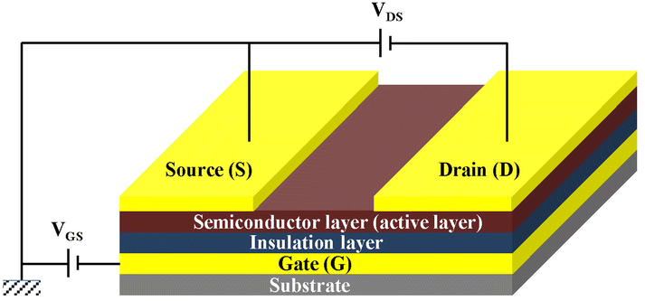 | ||
| Fig. 1 Schematic diagram of the typical architecture of an OTFT. | ||
Compared with small molecular thin-film transistor materials, polymeric thin film transistor materials are being actively explored because of their excellent mechanical properties, good solution processability and suitability for large area flexible production.3,4 Recently, driven by the trend of “flexibility” of electronics, flexible OTFTs with balanced electrical performance and mechanical stability constructed from polymers are acutely desired for applications in next-generation OTFTs. Polyurethane/ureas (PUUs) are a versatile class of organic polymers with repeated urethane (–NHCOO–) and/or urea (–NHCONH–) groups on the main chain that are formed by reacting polyols and/or polyamines with polyisocyanates in the presence of suitable catalysts and additives. In recent years, PUUs have been paid more attention by researchers in the field of OTFTs due to their excellent mechanical properties, good compatibility with organic semiconductors, high dielectric constant and wide adjustable performance range. For example, by using polyurethane (PU) as the insulation layer, Cremona et al. improved effectively the charge performance of OTFTs based on regioregular poly(3-hexyl thiophene) (rrP3HT), which showed a good hole mobility of up to 1.37 cm2 V−1 s−1 and an operating voltage as low as 10 V.5 Bao et al. prepared stretchable OTFTs which can bear up to 200% external strain using the PU elastomer as the insulation layer.6–8 Furthermore, the H-bonding between the characteristic groups in PUUs, i.e., urea and/or urethane bonds, and the unique phase separation structure derived from hard and soft segments are also powerful means to optimize the structure of the semiconducting layer of OTFTs. For example, Zhang et al. improved significantly the semiconducting performance of a diketopyrrolopyrrole (DPP)-based conjugated polymer through side-chain engineering via H-bonding derived from urea groups.9
Although a lot of reviews related to OTFTs have been published,4,10–17 a comprehensive summary of the recent progress of PUUs in OTFTs and their structure–function relationship is still scarce. In this review, the applications of PUUs in OTFTs are categorized according to the type of function of the device. In detail, the applications of PUUs in the semiconductor layer and insulation layer were systematically summarized and discussed separately. Meanwhile, the challenges of applying PUU to OTFTs were also emphasized. We hope that this review will not only become a resource summarizing what has been achieved in this field, but also provide effective guidance for future development of high-performance wearable/stretchable electronic devices.
2. Research of PUU in semiconductors
As a key component of OTFTs, the molecular structure and the molecular alignment of the semiconductor layer play a decisive role in charge transport. Most of the organic semiconductors consist of organic molecules with an extended π-conjugated structure, which lack flexibility due to their rigid backbone and semicrystalline nature. To improve the ductility of semiconductors, many strategies have been reported, such as reducing backbone regioregularity,18,19 inserting nonconjugated breaker into the backbone,20,21 introducing flexible fragments or side chains,22–24 blending with elastomers,16,25,26etc. Among them, PUUs have been widely investigated to regulate the properties of semiconductors due to their largely adjustable mechanical flexibility, which are based on their kaleidoscopic chemical structures and the special soft/hard phase separation in their microstructures. This work could be traced back to Zhang's publication on the use of urea chemistry to regulate semiconductor properties through side chain engineering via H-bonding.9The research of PUU in semiconductors could be divided into two categories. One is to implement PUU segments or the characteristic groups (–NHCOO– or –NHCONH–) of PUU into conjugated polymers, either in the backbone or on the sidechain, which greatly alters the structure and phase separation behavior of the semiconducting layer, hence their mechanical properties. The other is to modify the conjugated polymers during the semiconducting-layer deposition process, including physical blending of PUU with conjugated polymers and chemical cross-linking of conjugated polymers using urea/urethane chemistry.
2.1 Strategies based on structural alterations in conjugated polymers
Side chain engineering is one of the important strategies to optimize the performance of organic semiconductors.27 Previous studies have revealed that apart from the conjugated backbones, the side chains can dictate the self-organization of the polymer owing to the need for the side chains to form low-energy, space-filling structures.9,28,29 In many cases, the interactions between the side chains can exert an important influence on the inter-chain packing and backbone conformation, and as a result the thin-film microstructure and charge transport are affected.9In 2016, Zhang et al. introduced urea groups into side-chain engineering of conjugated polymers for the first time, and thus effectively improved the performance of DPP-quaterthiophene conjugated polymers (Fig. 2A, PDPP4T) in virtue of the H-bonding effect of the urea moiety.9 The research manifest that the incorporation of urea groups in the alkyl side chain not only promotes the lamellar packing of alkyl chains for thin films of polymers, but also induces better inter-chain π–π stacking of neighbouring conjugate backbones (Fig. 2B and C). These multiple effects facilitate the assemblies of PDPP4T into relatively long and wide nanofibers, which are well inter-connected within their thin films, and as a result a significant improvement in charge transport can be realized. In comparison with PDPP4T-0 without urea groups in the alkyl side chains, PDPP4T with urea-containing alkyl chains exhibits higher hole mobilities: thin-film mobility increases with the increase of urea group's content, and the highest hole mobility can reach 13.1 cm2 V−1 s−1. PDPP4T with a higher urea group content (>10 mol%) was not discussed, however, which might be due to that the strong H-bonding effect of urea moiety greatly decreased the solubility of polymer. Meanwhile, the presence of urea groups in the alkyl side chains also has a positive effect on the photovoltaic performances of PDPP4 after blending with PC71BM, which is mainly due to the microphase separation between the conjugated polymer and fullerene caused by the H-bonding between the urea groups in the side chains. Subsequently, this strategy was applied to thiazole-containing DPP-based polymers to further explore the effect of the urea groups on ambipolar semiconductors (Fig. 2D, PDPPTz2T).30 The results showed that the formation of hydrogen bonding derived from urea-containing side-chains enhanced the ambipolar semiconducting properties, both the mobilities and on/off ratios. Based on a similar strategy, Rondeau-Gagné et al. also demonstrated that urea-containing side-chains could significantly improve the semiconducting properties of isoindigo-based conjugated polymers (Fig. 2E).31 Unfortunately, these authors did not study the effect of the introduction of urea groups on the mechanical properties of semiconductors.
 | ||
| Fig. 2 (A and B) Chemical structures and assembly schematic of PDPP4T, (C) GIXRD patterns of PDPP4T deposited on OTS-modified SiO2/Si substrates (top) after thermal annealing at 100 °C, (D) chemical structures of PDPPTz2T, and (E) chemical structures of isoindigo-based conjugated polymers and average hole mobility for OTFTs fabricated from P1 to P4 with different urea contents after thermal annealing at 100 °C. Adapted with permission from ref. 9 Copyright (2016) American Chemical Society. Reprinted from ref. 30 Copyright (2018) American Chemical Society and ref. 31 Copyright (2018) the Royal Society of Chemistry. | ||
Aside from the urea group, the urethane group, another characteristic group of PUU, was also incorporated into the side chains of DPP-based polymers (PDPPurethane, Fig. 3A) by Yang and Oh, and the electrical performances and mechanical properties of semiconductors are discussed in detail.32 Compared with the urea group, the H-bonding strength between urethane groups is milder, which can be used as a dynamic bond to endow semiconductor thin films with good ductility and self-healing properties. Meanwhile, this softer H-bonding can also avoid the introduction of additional alkyl side chains to ensure the solubility of conjugated polymers, and thus facilitate the regular arrangement of H-bonding sites along the polymer backbone. The donor units have a great influence on the electrical performances and mechanical properties. Compared with thieno[3,2-b]thiophene (TT) and 2,2′-bithiophene (BT), the copolymer with 2-(2-(thiophen-2-yl)-vinyl)thiophene (TVT) as the donor showed better charge transport and ductility due to its better molecular planarity and the resultant stronger H-bonding and better lamellar packing of alkyl chains (Fig. 3B). The highest hole mobility reached 3.90 × 10⁻² cm2 V−1 s−1 and the polymer thin film maintained its original charge transport up to 100% external strain. This study further confirms that H-bonding side chain engineering is beneficial for improving the electrical performance and ductility of semiconductors, but the mobility and deformability, as well as the stability under stretching/releasing cycles still demand for continuous improvement.
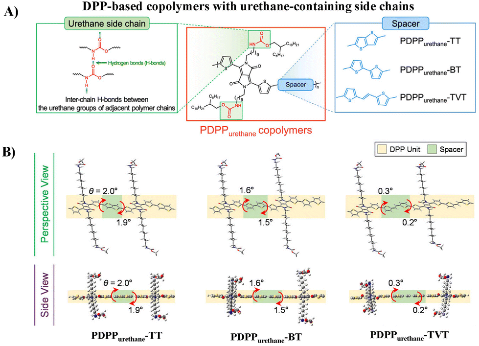 | ||
| Fig. 3 (A) Molecular structures of PDPPurethane copolymers and (B) perspective and side views of the calculated optimized geometries of the dimers of PDPPurethane copolymers using DFT computation. Adapted with permission from ref. 32 Copyright (2020) American Chemical Society. | ||
Similar to side-chain engineering, incorporation of soft nonconjugated segments into conjugate backbones is another common strategy to improve the ductility of semiconductors. For example, conjugated polymers containing polysiloxane or polyolefin coblocks endow semiconductor films with good stretchability up to 100% external strain.20,24,33 The key to this method lies in how to realize effective π–π stacking of conjugate backbones to ensure good charge transport. PUU is a multiblock copolymer composed of soft segments and hard segments arranged alternately along the macromolecular chain, in which soft segments and hard segments can be self-aggregated to form a special microphase separation. Once the hard segments, e.g. rigid conjugated domains, are well-connected, effective charge transport in both stretched and released states can be ensured.34 Inspired by this, Lipomi et al. reported a class of stretchable semiconducting block polymers (PDPP-b-PCL), in which the semiconducting blocks are based on the DPP unit flanked with furan rings and the soft nonconjugated blocks are poly(ε-caprolactone) (PCL) for the first time (Fig. 4A).35 The combination of stiff conjugated segments with flexible aliphatic polyesters produces materials that can be stretched >100% (Fig. 4B). The block polymer with more rigid PDPP segments exhibits better electronic behavior and can maintain its original field-effect mobility (∼1.0 cm2 V−1 s−1) even when the content of insulating PCL is up to 90 wt% (Fig. 4C). By optimizing the structure, Geng et al. synthesized the PU multiblock copolymer PU(DPP), containing a DPP-based rigid block and hydrogenated polybutadiene flexible block via a urethane linkage (Fig. 4D).36 The hard domains were formed by the aggregation of DPP blocks, which was enhanced by hydrogen bonds, whereas the flexible blocks provided a large free volume for deformability. Thus, a highly stretchable semiconductor with an elastic recovery (ER) of 82% at 175% strain, a crack onset strain (COS) of over 300% (Fig. 4E and F) and a maximum mobility of 0.19 cm2 V−1 s−1 was obtained, as the highest values of block copolymer-based stretchable semiconductors. Moreover, blending PU(DPP) with the fully conjugated polymer PDPP showed enhanced mobility (1.28 cm2 V−1 s−1) and good fatigue resistance (no obvious degradation of mobility at ε = 150% after 100 cycles of strain). This better performance is mainly attributed to the structural similarity of both components, enabling the blended film to form a uniform and stable microstructure against mechanical deformation and thermal treatment. These results confirm that the PU multiblock copolymers that provide proper phase separation are feasible to design intrinsically stretchable semiconductors, which provides a new idea for high performance stretchable semiconductors.
 | ||
| Fig. 4 (A) Synthetic strategy of PDPP-b-PCL, (B) determination of the effect of the PCL content in PDPP-b-PCL on mechanical properties (stress–strain curves were obtained from films suspended on water), (C) schematic illustration of the OTFT structure and relationships between the charge-carrier mobility and the PCL content, (D) synthetic route to the PU block copolymers PU(DPP), (E) mechanical properties of PU(DPP)x (X represents the content of DPP), and (F) cyclic tensile test under strain from 25% to 175% of PU(DPP). Reprinted from ref. 35 and 36 Copyright (2018, 2022) American Chemical Society. | ||
Müller et al. inverted the design principle and used a “soft” conjugated segment, polythiophenes with oligoethylene glycol side chains (P(g42T-T)), and a hard urethane segment to build stretchable semiconducting block polymers (Fig. 5A) P[P(g42T-T)-co-U], as shown in Fig. 4A.37 Copolymerization of P(g42T-T) and urethane segments results in a ductile material with a storage modulus of 25 MPa and an elongation at break of 95% due to the formation of a reversible H-bonding network derived from urethane-based blocks which reduces the ordering ability of the conjugated segment (Fig. 5B and C). Moreover, incorporation of hard urethane blocks only slightly reduces the electrical and electrochemical properties, yielding a material with a mobility of 0.2–0.7 cm2 V−1 s−1 when chemically doped or electrochemically oxidized, and a conductivity of about 20 S cm−1 was obtained when the material was doped with 2,3,5,6-tetrafluoro-7,7,8,8-tetracyanoquinodimethane (F4TCNQ). This report confirmed that the introduction of reinforcing segments is a promising strategy for modifying the mechanical and electrochemical properties of polar conjugated polymers. However, further study to create materials that do not show any trade-off between mechanical and electrochemical properties is still in high demand in this field.
 | ||
| Fig. 5 (A) Synthesis scheme of the copolymer P[P(g42T-T)-co-U], (B) WAXS diffractograms of a piece of P(g42T-T) (orange) and a free-standing film of P[P(g42T-T)-co-U] (blue) normalized to the intensity of the amorphous halo at 1.6 Å−1, and (C) tensile stress–strain curve of a free-standing P[P(g42T-T)-co-U] film (inset: photograph of a knotted P[P(g42T-T)-co-U] ribbon). Adapted with permission from ref. 37 Copyright (2021) John Wiley and Sons. | ||
2.2 Strategies based on postpolymerization modification
The aforementioned strategy has been mainly devoted to synthesize intrinsically semiconducting materials with both durable mechanical stability and excellent electrical performance, either by side-chain engineering or π-conjugated backbone engineering. However, this is a rather difficult goal to achieve, since (1) a careful balance must be found between H-bonding in the side chains and π–π stacking between the backbones, as they are two different types of interactions; if not well-balanced, this will result in insoluble materials that are hard to process; (2) the introduction of flexible but insulating segments in the backbone will lead to deteriorated electric performance. Dealing with such conflicting material design principles for good electronic properties and robust mechanical properties is still a challenge. Postpolymerization modification is an alternative strategy to optimize the mechanical properties of polymeric semiconductors. The reported methods include physical blending of the conjugated polymer with elastomeric polymers or small molecular additives, such as chemical cross-linkers.38,39Even though crosslinking of polymers typically leads to an increase in elastic modulus, studies have shown that crosslinking in conjugated polymers can suppress crystallization by reducing polymer chain rearrangement and aggregation and thus improve the ductility of polymer semiconductors.40,41 In 2016, Bao et al. first reported a stretchable DPP-based polymeric system through covalently crosslinking the polymer with flexible oligo-siloxane.41 The cross-linked film can maintain a steady hole mobility (0.4 cm2 V−1 s−1) after 500 strain-release cycles at 20% strain. Based on these results, they further investigated the effect of the “hardness” of cross-linkers on the electronic performance and mechanical properties of the DPP-based polymer via systematic tuning the cross-linker's crystallinity (Fig. 6).42 They synthesized four cross-linkers, using perfluorophenyl azide (PFPA) as the terminal reactive group, which can release nitrogen gas and form a singlet nitrene upon thermal or photoactivation to attack available sp3 C–H bonds on the alkyl side chains to form covalent cross-links (Fig. 6B). Compared with the linear cross-linker containing ester groups, the linear cross-linker containing carbamate groups are more crystalline; by introducing alkyl branches, both cross-linkers become amorphous (Fig. 6C, Linear-H, Linear, Branch-H and Branch). Partially formed hydrogen bonding was observed for Branch-H, while fully formed hydrogen bonding was observed for Linear-H. Compared to uncrosslinked polymers, all crosslinked polymers exhibited better mechanical properties, with both improved fracture strain and crack onset strain (COS). Among them, the DPP polymer crosslinked by Branch-H showed the best COS over 100%. On the other hand, the polymer crosslinked by Linear-H readily underwent phase separation to form cross-linked domains that obstructed the strain distribution of the polymer film and formed a rougher surface (Fig. 6D), which resulted in the worst COS of 75%, but still better than that of the un-crosslinked one (25%). This implies that decreasing the crystallinity of the crosslinker but still maintaining its ability to form hydrogen bonding is important to obtain polymers with excellent mechanical properties. Among the polymers, polymers crosslinked by Branch-H and Branch exhibited the robustest mobility against mechanical deformation, with μh values remaining >0.1 cm2 V−1 s−1 at 2000 cycles with ε = 25% (Fig. 6E). However, it should be pointed out that the crosslinkers with the urethane group did not exhibit obviously better electric/mechanical performance than their ester counterparts, illustrating the complexity of energy dissipation via H-bonding in polymer films.
 | ||
| Fig. 6 (A) Chemical structure of the DPP-based polymer, (B) the simplified scheme of the perfluorophenyl azide (PFPA) cross-linking reaction, (C) the structures of four cross-linkers, (D) bright field optical microscopy (top) and atomic force microscopy (bottom) images of cross-linked polymer films (the left panel of 5Linear-H displays the morphology of the precured film, whereas the right panel shows the cross-linked film morphology), and (E) average mobility of relaxed polymer films after various stretching cycles. Adapted with permission from ref. 42 Copyright (2019) American Chemical Society. | ||
Blending with elastomers is another effective strategy for preparing stretchable semiconductors. Studies have shown that, despite the presence of an insulating polymer phase, the blend system can possess good semiconductor properties under controlled conditions.43–47 For example, Cho et al. prepared a flexible OTFT device based on P3HT/PMMA or P3HT/PS blend films, which exhibited similar charge transport compared to that of neat P3HT films.48,49 In 2019, Lee et al. constructed OTFT devices by a bottom-contact top gate architecture, using blended P3HT/thermoplastic polyurethane (TPU) elastomer films as the semiconductor active layer (Fig. 7A).50 The results show that the Young's modulus and tensile strength of the blended films increase with the increase of TPU content (from 1![[thin space (1/6-em)]](https://www.rsc.org/images/entities/char_2009.gif) :1 to 7:3, w:w), but the elongation at break and charge transport decreases gradually (Fig. 7B). When the blending ratio is 1:1, the film shows the highest average mobility (1.46 × 10⁻³ cm2 V−1 s−1) while possessing adequate mechanical strength (21 MPa) with an elongation strain (∼120%) (Fig. 7C). Moreover, stretchable fabric transistors based on P3HT/TPU were fabricated using graphene/Ag composites as zigzag fabric source/drain electrodes, an elastic ionic-gel polymer as the dielectric material, an ionic liquid as the transporter, together with PDMS/EGaIn as the flexible gate electrode, on the surface of a filament TPU substrate. The devices exhibited excellent stretchability (∼50%) while maintaining good electrical properties (the average charge carrier mobility of 1.74 cm2 V−1 s−1, the on/off current ratio of 104) and showed good electrical stability up to 1000 cycles of stretch/release testing (Fig. 7D–F). This good stability is mainly due to the similarity in the elasticity and flexibility of all the components in the device, which enables synchronized deformation of the substrate and channel layer. This implies that the similarity of all components in the structure or mechanical properties is the key to obtain high performance stretchable devices.
:1 to 7:3, w:w), but the elongation at break and charge transport decreases gradually (Fig. 7B). When the blending ratio is 1:1, the film shows the highest average mobility (1.46 × 10⁻³ cm2 V−1 s−1) while possessing adequate mechanical strength (21 MPa) with an elongation strain (∼120%) (Fig. 7C). Moreover, stretchable fabric transistors based on P3HT/TPU were fabricated using graphene/Ag composites as zigzag fabric source/drain electrodes, an elastic ionic-gel polymer as the dielectric material, an ionic liquid as the transporter, together with PDMS/EGaIn as the flexible gate electrode, on the surface of a filament TPU substrate. The devices exhibited excellent stretchability (∼50%) while maintaining good electrical properties (the average charge carrier mobility of 1.74 cm2 V−1 s−1, the on/off current ratio of 104) and showed good electrical stability up to 1000 cycles of stretch/release testing (Fig. 7D–F). This good stability is mainly due to the similarity in the elasticity and flexibility of all the components in the device, which enables synchronized deformation of the substrate and channel layer. This implies that the similarity of all components in the structure or mechanical properties is the key to obtain high performance stretchable devices.
 | ||
| Fig. 7 (A) Device configuration of the thin-film transistor based on the P3HT/TPU blend film, (B) charge carrier mobility as a function of the P3HT content, (C) typical strain–stress curves of P3HT/TPU blend films with blending ratios of 5/5, 4/6, and 3/7, (D) schematic illustration of the fiber transistor based on buckled hybrid fiber electrodes, (E) changes in the μ and VT values of the device as a function of strain, and (F) changes in the μ and VT values of the device obtained after cyclic stretching tests at ∼50% strain. Adapted with permission from ref. 50 Copyright (2019) Elsevier. | ||
3. Research of PUU in the insulation layer
The insulation layer is another important component of OTFTs. The structure of the insulation layer has a decisive influence on the operating voltage, current switching ratio and subthreshold swing of the device, which is usually evaluated with the capacitance or dielectric constant of the insulator. In addition, because the conductive channel of OTFTs is mainly located in several molecular layers within the semiconductor layer close to the interface between the insulator layer and the semiconductor layer, the growth quality of the semiconductor on the interface has a great impact on charge transport. The properties of the insulator layer, such as its smoothness, the functional group on its surface and its interactions with the organic semiconductors, may determine the quality of the crystalline domains of the organic semiconductors to a large extent. Therefore, the performance of the device can be optimized and improved significantly by proper design of the insulating material and its surface properties.Compared with the traditional inorganic dielectric, the polymeric dielectric has better contact with the organic semiconductor layer and a similar Young's modulus to the organic semiconductor layer, which is suitable for large-area solution-processing for flexible electronics. Furthermore, the structure of polymeric dielectric can be easily modified, leaving large room for performance improvement. Reported polymer dielectrics include polymethyl methacrylate (PMMA), polyfluorinated olefin (e.g. CYTOP), polyvinyl alcohol (PVA), polystyrene (PS), polyimide (PI), poly(vinylphenyl) (PVP), PUU, etc.51–55 Among them, PUU has gained increasing attention from researchers as an insulating layer in OTFTs recently, due to its excellent mechanical properties, high dielectric constant and wide adjustable performance. This work could be traced back to the related report of Murata et al. in 2007, which used dipole-polarized PUA as the gate insulator layer to regulate the threshold voltage of OTFTs.56
3.1 Polyurethane (PU)
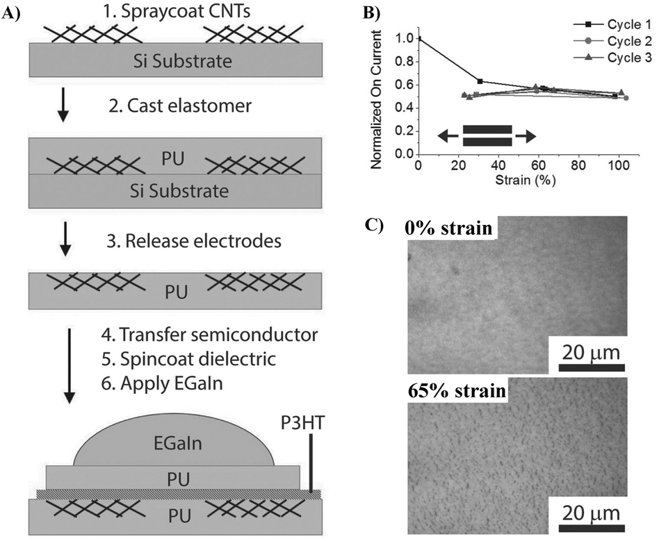 | ||
| Fig. 8 (A) Schematic of the device fabrication process, (B) normalized ION for three cycles to 100% strain demonstrating reproducible strain-independent characteristics, and (C) effect of strain on the structure and morphology of the PU/P3HT/PU film under different strains. Adapted with permission from ref. 8 Copyright (2014) John Wiley and Sons. | ||
The good compatibility of PU with the fabric and the capability to form a smooth surface of PU make it a good candidate to fabricate flexible OFETs, since the smoothness of the gate dielectric is an essential factor in obtaining good performance. Otherwise, a thicker semiconductor layer should be employed to mitigate the degradation caused by rough gate dielectric surfaces. For example, a surface-smoothing process reported by Song et al. endows the fabricated OTFTs based on PU-coated polyethylene terephthalate (PET) fabric substrates with improved charge transport properties and good flexibility, which could be used as driving devices for active matrix organic light emitting diode (AMOLED) display panels (Fig. 9A–C).58,59 PU as an additional dielectric layer on the inorganic gate dielectric (SiO2) reported by Busnaina et al. also imparts the printed OTFTs with a high ON/OFF ratio and decent mobility (Fig. 9).60 OTFTs were fabricated on a PU coated silicon substrate using an electrophoretic directed assembly based inking process (Fig. 9D), which shows an on/off ratio of approximately 105 and a field effect mobility of 6.4 × 10⁻³ cm2 V−1 s−1 (Fig. 9E).
 | ||
| Fig. 9 (A) The structure of polymer coating layers and OTFTs fabricated on fabric substrates (the first layer (PU) to reduce the large surface roughness of the fabric substrates and the second layer (PA) to enhance the compatibility of the first layer with OTFT processes) and (B) picture of cotton cloth attached with PET fabric containing OTFTs (the fabric was naturally bent and folded along the winkles of the cloth). Reprinted from ref. 58 and 59 Copyright (2014, 2016) Elsevier. (C) Pictures of SEM and AFM of the bare PET fabric and the PU/PET fabric coated by PU, (D) schematic illustration of the electrophoretic directed assembly based inking of the Damascene template and the subsequent transfer printing of the CNT patterns, and (E) transfer and output characteristics of the fabricated OTFT device with transfer printed CNT source/drain electrodes. Reprinted from ref. 60 Copyright (2019) American Institute of Physics. | ||
3.1.2.1 PU with specially-designed functional groups. Cross-linking is regarded as a promising approach to enhancing the dielectric properties of polymers.61 For example, Kim et al. increased the dielectric constant of PVA from 6.2 to 12.6 by a cross-linking method.62 Furthermore, crosslinking can facilitate the formation of dense films and thus reduce the thickness of the dielectric layer, which is conducive to improving the performance of OTFT devices. Generally, fabricating an ultrathin polymer gate dielectric layer with a non-pinhole structure over large areas is very difficult.61,63 By introducing olefin groups into the side chain, a crosslinked PU dielectric layer could be obtained when exposed to UV light (Fig. 10A), and the corresponding para-sexiphenyl (p-6P)/vanadyl-phthalocyanine (VOPc) OTFT device (Fig. 10B) exhibits an ultra-low leakage current (less than 1 × 10⁻⁵ A cm−2) as well as a decent mobility (0.13 cm2 V−1 s−1) and a high on/off ratio (104).64 The conspicuous improvement in decreasing the leakage current was attributed to the lower free volume and non-pinhole surface morphology of the polymer film after crosslinking (Fig. 10C). However, the threshold voltage of the device was high (−13 V) since the dielectric constant of the developed PU insulating layer was relatively low (3.2). Subsequently, inorganic ZrO2 was integrated into the crosslinked PU insulation layer by the same research group to improve the dielectric constant (Fig. 10D).65 An organic–inorganic hybrid gate insulation layer with a dielectric constant of 3.9 was obtained and the fabricated p-6P/VOPc OTFTs showed improved device performances with a mobility of 0.56 cm2 V−1 s−1 and a threshold voltage of −6 V. However, the incompatibilities between the organic and inorganic components might lead to microphase separation, resulting in an increased leakage current. Further optimization includes introducing the polar cyano group into the side chain of PU to obtain crosslinked PU with a higher dielectric constant (7.3) (Fig. 10E); however, the induced dipoles derived from polar groups under gate voltage also act as carrier traps and deteriorate charge transport.66
 | ||
| Fig. 10 (A) The fabrication and UV curable process of photosensitive PU, (B) schematic of a bottom-gate top-contact p-6P/VOPc OTFT device geometry, (C) the tapping mode AFM image of the photosensitive PU, (D) schematic of the cross-linked PU containing cyanogroup, and (E) synthesis of the ZrO2/PU composite. Reprinted from ref. 64 and 66 Copyright (2016, 2018) the Royal Society of Chemistry and ref. 65 Copyright (2012) Elsevier. | ||
To improve the dielectric constant, the Pei group synthesized a new PU-PEG copolymer consisting of a PU-co-PEG main chain and PEG side chains (Fig. 11A).67 PEG was selected as the main chain for its high flexibility, low monomer viscosity which is important for printing, high dielectric constant and semicrystalline structure of its homopolymer. PEG was selected to introduce side chains with its high polarity and chain mobility at room temperature. Such an engineering design strategy endows the resulting elastomeric dielectric copolymer with the optimal overall performance, including a high dielectric constant (as high as ∼13 at 12 Hz), high optical transmittance (>90% at 550 nm), and sufficient elongation at break (>50%) (Fig. 11B). A stretchable device using this PU-PEG copolymer as the insulating layer showed significant improvement in device performance. The devices can be stretched with up to 50% strain and subjected to 500 cycles of repeated stretching with 20% strain without significant loss in electrical properties (Fig. 11C and D). However, the device still exhibited hysteresis in the transfer curve due to the thick film thickness (∼1.1 μm) of the dielectric layer used to repress the gate leakage current.61 Based on the same strategy, Earmme et al. synthesized PU triblock copolymers comprising polycarprolactone diol (PCL), 1,6-hexam-ethylene diisocyanate (HMDI) and PEG, in which PCL with high crystallinity was used to stabilize the total interfacial polarization of the resulting dielectric films (Fig. 11E).68 Thin films of the resulting PU gate dielectrics exhibited excellent insulating properties (∼7 × 10⁻⁷ A cm−2 at 1 V) as well as large areal capacitance (170 nF cm−2) with a film thickness of ∼50 nm. The fabricated OTFTs using N,N‘-ditridecylperylene-3,4,9,10-tetracarboxylic diimide as the organic semiconductor show decent n-channel activity (0.023 ± 0.014 cm2 V−1 s−1) with negligible hysteresis at a low operating voltage of 1 V (Fig. 11F and G). However, the stability of such engineering devices in atmospheric environments is still questionable due to the high hydrophilicity of PEG. In contrast, Cremona et al. declared that reducing the content of electric dipoles (low polarity) in PU is also beneficial for improving the charge transport performance of OTFTs.5 They obtained p-type OTFTs using P3HT as the semiconductor and low polarity PU as the dielectric layer. A high hole mobility of up to 1.37 cm2 V−1 s−1 was observed together with an ON/OFF current ratio higher than 103 and an operating threshold voltage as low as −10 V (Fig. 12A and B).
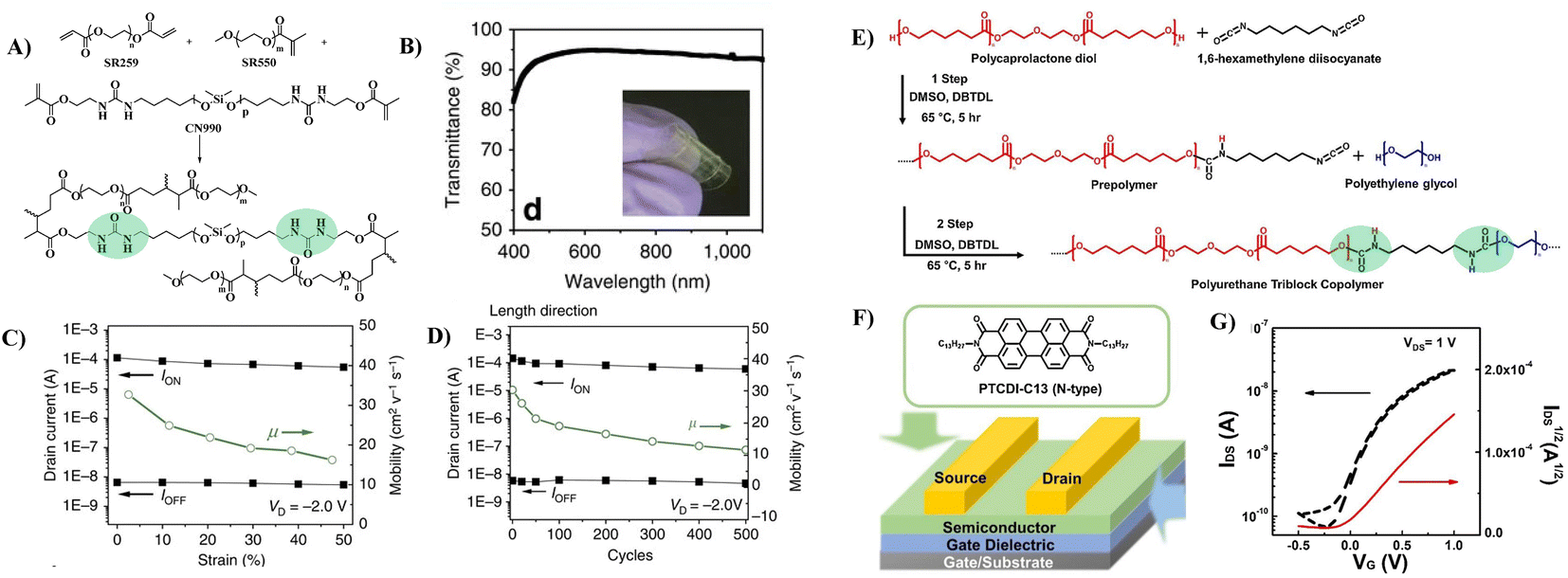 | ||
| Fig. 11 (A) Schematic illustration of the PU-PEG copolymer, (B) optical transmittance of a constructed transistor array, (C) ION, IOFF and mobility as a function of applied strain along the channel length direction, (D) plots of ION and IOFF at 0% strain during 500 cycles of continuous stretching–relaxation between 0 and 20% strains along the channel length direction, (E) synthesis of the polyurethane triblock copolymer, (F) schematic of the top-contact/bottom-gate OTFT and chemical structures of organic semiconductors, and (G) transfer characteristics of OTFT devices. Reprinted from ref. 67 Copyright (2015) Springer Nature and ref. 68 Copyright (2019) Elsevier. | ||
 | ||
| Fig. 12 (A) OTFTs in the bottom contact-top gate configuration, (B) the chemical structure of PU and the regioregular poly-(3-hexylthiophene) (rrP3HT), (C) synthesis of polyurethane containing terphenyl, (D) device configuration and performance with p-6p as a semiconductor, and (E) AFM topography images of a p-6P layer on PU with different terphenyl contents. Reprinted from ref. 5 and 70 Copyright (2018, 2014) Elsevier. | ||
The surface of the dielectric material layer can be further functionalized, which can have an impact on the growth of the semiconductor crystals and thus have an unneglectable effect on the carrier mobility of the devices.66,69 Cui et al. explored the influence of surface functionalization of the PU dielectric layer on the grain size and the charge carrier mobility.66,70 For this purpose, triphenyl groups were incorporated into the side chain of PU (Fig. 12C).70 The crystal size of the p-6P semiconductor layer can be adjusted due to the presence of triphenyl in the insulating layer, which has a similar structure to p-6P and thus provides a crystal nucleus for p-6P and induces its crystallization on the surface (Fig. 12D and E). Increasing the amount of the triphenyl in the PU dielectric resulted in a significant decrease in the crystal size of the p-6P semiconductor (Fig. 12E). The result illustrates that p-6P OTFTs with a suitable grain size of the p-6P semiconductor exhibit improved charge carrier mobility. A similar phenomenon was also observed when benzene was incorporated into the side chain of PU (Fig. 10E).66
3.1.2.2 Strategies based on complex technology. Combining elastic dielectrics with compounds that have high capacitances to improve their dielectric properties is the widely used strategy for the fabrication of stretchable low-voltage OTFTs. One of the typical cases is ionic glue, where an ionic conducting liquid is immobilized inside a polymer matrix. Ionic glue exhibits large specific capacitance due to the production of an electrical double layer (EDL) at ion-gel/semiconductor and ion-gel/gate electrode interfaces under an electric field. Kim et al. first reported the utilization of an ionic PU as a stretchable dielectric for stretchable OTFTs.71 An ion-gel dielectric consisting of PU and 1-ethyl-3-methylimidazolium bis(trifluoromethylsulfonyl)imide ([EMIM][TFSI]) ionic liquid was fabricated onto the channel material made of poly[4,8-bis(5-(2-ethylhexyl)-thiophen-2-yl)benzo[1,2-b;4,5-b′]dithiophene-2,6-diyl-alt-(4-(2-ethylhexyl)-3-fluorothieno[3,4-b]thiophene)-2-carboxylate-2-6-diyl] (PTB7-Th) (Fig. 13A). The ionic PU is transparent and stretchable and exhibits a large specific capacitance of 5.5 μF cm−2 (Fig. 13B and C). The developed free-standing ionic PU-based coplanar OTFTs exhibited a hole mobility as high as 7.9 cm2 V−1 s−1 and operated in the low-voltage regime (VDS = 1.0 V, VGS = 2.5 V) and demonstrated high bendability (radius of curvature: 7.2 mm) (Fig. 13D–F). Moreover, by introducing a poly(3,4-ethylenedioxythiophene):polystyrene sulfonic acid layer (PEDOT:PSS) as the electrode, they fabricated free-standing, fully stretchable, coplanar-type all-organic OTFTs with a high mobility of up to 17.8 cm2 V−1 s−1 (Fig. 13G). These all-organic devices withstand stretching up to 80% tensile strain and the mobility was decreased only by 15%–20%, even after 1000 cycles under a tensile strain of 20% (Fig. 13H and I). Meanwhile, they optimized the preparation process of the insulation layer and developed a bilayer dielectric with a neat polyurethane top layer and a bottom ionic PU layer, which further increased the capacitance of the insulation layer (30 μF cm−2) and reduced the operating voltage of the device (2 V) (Fig. 14A and B).72 The formation of a combined electric double layer and dipole polarization in the ionogel/PU layers account for these excellent dielectric properties. The ionic PU was also used as the gate dielectric to construct indium gallium zinc oxide (IGZO)-based thin film transistors.73,74 The large capacitance of the ionic PU allowed one to operate the transistor at a very low threshold voltage (0.3 V). While an ion-gel dielectric can offer large capacitance, the microphase separation caused by physical blending still leads to high leakage current. Meanwhile, the switching speeds of thin film transistors are often limited by the relatively slow movement speed of the ionic molecules, which ultimately limits the frequency at which the devices can operate reliably.75 Furthermore, the ions are liable to aggregate into large ionic domains which cannot follow high frequency alternating electric fields, resulting in a much lower-than-expected increase in dielectric constant.76
 | ||
| Fig. 13 (A) Molecular structures to form a solid-state ionic PU elastomer electrolyte, (B) optical characteristics of a transparent ionic PU film, (C and D) schematic diagram and optical microscopy image of ionic PU-based free-standing, coplanar OTFT with Au source, drain, and gate electrodes, (E) transfer (IDS–VGS) characteristics of ionic PU electrolyte-gated OTFTs under each bending radius (Rc) (effective strains of each Rc correspond to 0%, 1.4%, 2.1%, 2.6%, 3.0%, and 3.4%, respectively), (F) mobility and threshold-voltage variation under various Rcs along the convex direction in the ionic PU electrolyte-gated OTFTs, (G) schematic and optical microscopy image of free-standing coplanar type all-organic transistors fabricated by forming the PEDOT:PSS electrode and PTB7-Th semiconducting polymer film onto the ionic PU electrolyte film, (H) normalized mobility (μ/μ0) measured under various tensile strains applied in the vertical and horizontal directions, and (I) reliability characteristics investigated by measuring the mobilities after repeated stretching cycles with 20% strain up to 1000 cycles. Reprinted from ref. 71 Copyright (2019) John Wiley and Sons. | ||
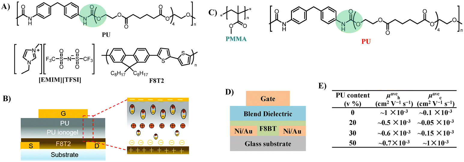 | ||
| Fig. 14 (A) Chemical structures of the PU elastomer, [EMIM][TFSI] ionic liquid, and the F8T2 polymer semiconductor, (B) schematic diagram of the top-gate bottom-contact OTFT architecture (left) and polarization mechanism of PU ionogel/PU bilayer gate dielectrics (right), (C) chemical structures of the polymer blend dielectrics used in this study: PMMA and PU, (D) cross-sectional diagram of top-gate bottom-contact OTFT, and (E) PU content dependence mobility of F8BT OTFTs with PMMA–PU blends in p- and n-channels. Reprinted from ref. 72 Copyright (2020) the Royal Society of Chemistry. | ||
Noh et al. developed ambipolar poly(9,9-dioctylfluorene-alt-benzothiadiazole) (F8BT) OTFTs employing polymer dielectric blends of PMMA and the PU elastomer (Fig. 14C and D).77 With the increase of PU (0–50 v%) in the PMMA–PU blend dielectrics, the electron mobility increases significantly, resulting in nearly perfect ambipolar characteristics with hole and electron mobilities of 6.0 ± 0.7 × 10⁻⁴ and 9.7 ± 0.4 × 10⁻⁴ cm2 V−1 s−1, respectively, in a PU:PMMA blend of 50:50 v% (Fig. 14E). The remarkable trend ensues from trapping of hole carriers at the dielectric/semiconductor by the –N–H– and carbonyl group (C![[double bond, length as m-dash]](https://www.rsc.org/images/entities/char_e001.gif) O) interface dipoles in the PU dielectric.
O) interface dipoles in the PU dielectric.
3.2 Polyurea (PUA)
Compared to PUs with a dielectric constant of above 3.0, PUAs have a higher dielectric constant of above 5.0 due to the strong polarity of urea moieties.78 Moreover, strong intermolecular hydrogen bonding between the urea bonds in the polymer backbone endows PUA materials with high insulating properties by producing dense films with a suppressed free volume. However, a trade-off between the dielectric properties of PUA materials and their solubility needs to be optimized carefully.In 2007, Murata et al. first reported utilizing PUA as a gate dielectric for OTFTs (Fig. 15A).56 PUA was polarized by corona poling to generate uniformly oriented dipoles, and thus formed an internal electric field, which induced the mobile charge carrier in the semiconductor layer at the semiconductor–dielectric interface (Fig. 15B and C). As a result, the operation voltage shifts to a lower voltage (less than 6 V). However, the mobility of pentacene OTFTs using dipole-polarized PUA as a gate dielectric (0.044 cm2 V−1 s−1) was about half of that obtained with a non-polarized PUA gate dielectric (0.077 cm2 V−1 s−1), which was attributed to the larger Coulombic interaction between charge carriers and induced dipoles of gate dielectrics. In another study, Jang and Kim et al. investigated the effect of hydrogen bonding of PUA on the insulating properties by varying the types of comonomers (Fig. 15D).79 They found that as the number of substituted alkyl groups increases, the dielectric constant and insulation properties decreased (Fig. 15E). This is due to the weakened hydrogen-bonding, as the size of the alkyl groups increases, hydrogen bonding is more difficult to form. It should be noted that DI-2 (1.4-phenylene diisocyanate) based PUA with stronger hydrogen-bonding and a better packing structure did not dissolve in common polar aprotic solvents. Because of the strong hydrogen bonding between the PUA main chains, non-pinholes and a densely thin PUA film (60 nm) were successfully fabricated through a solution process and showed a high dielectric constant of >5.8, a capacitance of 88 nF cm−2 and excellent insulating characteristics (leakage current less than 10−9 A cm−2 at 2 MV cm−1). Although a high dielectric constant was realized, the urea group present on the surface of the gate insulator acts as a charge-carrier trap to degrade charge transport (Fig. 15E). Alternatively, this negative effect could be suppressed through surface treatment, and the excellent device characteristics of OTFTs could be obtained (Fig. 15E). To avoid excessive hydrogen bonding, the Zhang group used PUU as the dielectric and fabricated an intrinsically stretchable thin film transistor device using semiconducting single-walled carbon nanotubes (SWNTs) as the channel material.80 The realized devices achieved excellent electrical and mechanical properties simultaneously.
 | ||
| Fig. 15 (A) Reaction scheme of PUA by vapor deposition polymerization, (B and C) schematic representations of the corona poling process of PUA gate dielectrics and OTFTs with polarized gate dielectrics, (D) molecular structure of a variety of DI and DA and synthesized PUAs, and (E) dielectric and insulating properties of PUA thin films (60 nm-thick) and electrical characteristics of OTFTs with PUAs and surface treated-PUA gate insulators. Reprinted from ref. 56 Copyright (2007) American Institute of Physics and ref. 79 Copyright (2018) American Chemical Society. | ||
4. Conclusion and outlook
The design and development of electronic devices must meet the main needs of society, where energy-saving and flexibility are the current requirements. In addition, the rapid development of the times has also given more stringent requirements for energy-saving and flexibility. Flexibility means that the materials need to meet both high deformation and excellent fatigue resistance; energy-saving means that not only the energy consumption of the device should be considered, but energy that is consumed during the production process for both the materials and the devices should be included. Thus, developing flexible OTFTs with low energy consumption or low operating voltage has become extremely critical. PUUs have inherent advantages in the preparation of flexible and low operating voltage OTFTs due to their excellent mechanical toughness, solution-processability, high dielectric constant and variability for structural design. Therefore, we summarized the application of PUUs in OTFTs in this review.Enhancing the capacitance or dielectric constant of PUU dielectrics is an effective way to achieve low operating voltage OTFFs. The published reports have well proved the effectiveness of this method. However, it is very challenging to achieve a low operating voltage of the device while maintaining the original charge transport properties. In this respect, the authors believe that ionic PUU has a bright future, but the reported molecular structure still needs further optimization. For semiconductors, a trade-off between high deformation (>100%), solution-processability and high charge transport is still a stumbling block for researchers. Although side chain engineering is an effective strategy for improving the solubility and charge transport of semiconductors, it is difficult to achieve a deformation of more than 100%. In contrast, regulating the conjugated backbone of semiconductors by PU chemistry, such as the introduction of a microphase separation structure, will be an effective way to solve the trade-off. Relevant contributions have only been reported in recent years. Therefore, the authors believe that the research in this area will also be a very promising research direction for stretchable high performance semiconductors.
In addition, the synergistic design of OTFT components, including electrodes, the substrate, the semiconductor layer and the insulator layer, is also critical to the improvement of the overall device performance. For example, interface stripping caused by asymmetric deformation between the semiconductor and the insulator layer, and high contact resistance caused by incompatibility between the electrode and the insulator layer are important reasons for the deterioration of the device performance. Therefore, the authors believe that, based on the variability of the structural design of PUU, all the components of the device are designed to have similar deformability and similar structural composition will be a significant, profound and worth exploring direction to obtain stretchable OTFTs with low operating voltages and high electronic performances.
This review shows that only a part of the huge variety of possible OTFT structures has been explored hitherto. There is enormous potential in this field awaiting exploration, which may lead to new synthetic methods and new materials with interesting properties and practical applications.
Author contributions
Y. M. wrote the article. Q. S. edited the manuscript before submission. X. W. contributed to the discussion and wrote the article.Conflicts of interest
The authors declare no competing interests.Acknowledgements
This work was supported by the Hubei Provincial Natural Science Foundation of China (2023AFB1030), the National Natural Science Foundation of China (NSFC 22075105 and 51603223) and the start-up funding from Jianghan University.References
- Y. Qian, X. W. Zhang, L. H. Xie, D. P. Qi, B. K. Chandran, X. D. Chen and W. Huang, Adv. Mater., 2016, 28, 9243–9265 CrossRef CAS PubMed.
- T. Q. Trung and N. E. Lee, Adv. Mater., 2017, 29, 1603167 CrossRef PubMed.
- D. Kim and F. S. Kim, Chem. Mater., 2021, 33, 7572–7594 CrossRef CAS.
- S. E. Root, S. Savagatrup, A. D. Printz, D. Rodriquez and D. J. Lipomi, Chem. Rev., 2017, 117, 6467–6499 CrossRef CAS PubMed.
- H. C. Avila, P. Serrano, A. R. J. Barreto, Z. Ahmed, C. D. Gouvea, C. Vilani, R. B. Capaz, C. F. N. Marchiori and M. Cremona, Org. Electron., 2018, 58, 33–37 CrossRef CAS.
- D. Kong, R. Pfattner, A. Chortos, C. Lu, A. C. Hinckley, C. Wang, W.-Y. Lee, J. W. Chung and Z. Bao, Adv. Funct. Mater., 2016, 26, 4680–4686 CrossRef CAS.
- A. Chortos, G. I. Koleilat, R. Pfattner, D. Kong, P. Lin, R. Nur, T. Lei, H. Wang, N. Liu, Y.-C. Lai, M.-G. Kim, J. W. Chung, S. Lee and Z. Bao, Adv. Mater., 2016, 28, 4441–4448 CrossRef CAS PubMed.
- A. Chortos, J. Lim, J. W. F. To, M. Vosgueritchian, T. J. Dusseault, T.-H. Kim, S. Hwang and Z. Bao, Adv. Mater., 2014, 26, 4253–4259 CrossRef CAS PubMed.
- J. Yao, C. Yu, Z. Liu, H. Luo, Y. Yang, G. Zhang and D. Zhang, J. Am. Chem. Soc., 2016, 138, 173–185 CrossRef CAS PubMed.
- X. W. Yin, J. L. Yang and H. B. Wang, Adv. Funct. Mater., 2022, 32, 2202071 CrossRef CAS.
- J. Lee, B. L. Zambrano, J. Woo, K. Yoon and T. Lee, Adv. Mater., 2020, 32, 1902532 CrossRef CAS PubMed.
- F. M. Wu, Y. X. Liu, J. Zhang, S. M. Duan, D. Y. Ji and H. Yang, Small Methods, 2021, 5, 1700429 Search PubMed.
- X. M. Wang, Y. Q. Liu, Q. Z. Chen, Y. J. Yan, Z. C. Rao, Z. X. Lin, H. P. Chen and T. L. Guo, J. Mater. Chem. C, 2021, 9, 7796–7828 RSC.
- M. Ashizawa, Y. Zheng, H. Tran and Z. A. Bao, Prog. Polym. Sci., 2020, 100, 101181 CrossRef CAS.
- Q. Zhang, J. Y. Huang, K. Wang and W. Huang, Adv. Mater., 2022, 34, 2110639 CrossRef CAS PubMed.
- L. Janasz, M. Borkowski, P. W. M. Blom, T. Marszalek and W. Pisula, Adv. Funct. Mater., 2022, 32, 2105456 CrossRef CAS.
- J. Y. Chen, J. Yang, Y. L. Guo and Y. Q. Liu, Adv. Mater., 2022, 34, 2104325 CrossRef CAS PubMed.
- Y.-C. Lin, Y.-W. Huang, C.-C. Hung, Y.-C. Chiang, C.-K. Chen, L.-C. Hsu, C.-C. Chueh and W.-C. Chen, ACS Appl. Mater. Interfaces, 2020, 12, 50648–50659 CrossRef CAS PubMed.
- H. Park, B. S. Ma, J.-S. Kim, Y. Kim, H. J. Kim, D. Kim, H. Yun, J. Han, F. S. Kim, T.-S. Kim and B. J. Kim, Macromolecules, 2019, 52, 7721–7730 CrossRef CAS.
- J. Mun, G.-J. N. Wang, J. Y. Oh, T. Katsumata, F. L. Lee, J. Kang, H.-C. Wu, F. Lissel, S. Rondeau-Gagné, J. B.-H. Tok and Z. Bao, Adv. Funct. Mater., 2018, 28, 1804222 CrossRef.
- J. Y. Oh, S. Rondeau-Gagné, Y. C. Chiu, A. Chortos, F. Lissel, G. N. Wang, B. C. Schroeder, T. Kurosawa, J. Lopez, T. Katsumata, J. Xu, C. Zhu, X. Gu, W. G. Bae, Y. Kim, L. Jin, J. W. Chung, J. B. Tok and Z. Bao, Nature, 2016, 539, 411–415 CrossRef CAS PubMed.
- L. A. Galuska, M. U. Ocheje, Z. C. Ahmad, S. Rondeau-Gagné and X. Gu, Chem. Mater., 2022, 34, 2259–2267 CrossRef CAS.
- H.-C. Yen, Y.-C. Lin and W.-C. Chen, Macromolecules, 2021, 54, 1665–1676 CrossRef CAS.
- K. Ditte, J. Perez, S. Chae, M. Hambsch, M. Al-Hussein, H. Komber, P. Formanek, S. C. B. Mannsfeld, A. Fery, A. Kiriy and F. Lissel, Adv. Mater., 2021, 33, 2005416 CrossRef CAS PubMed.
- S. Zhang, Y.-H. Cheng, L. Galuska, A. Roy, M. Lorenz, B. Chen, S. Luo, Y.-T. Li, C.-C. Hung, Z. Qian, P. B. J. St Onge, G. T. Mason, L. Cowen, D. Zhou, S. I. Nazarenko, R. F. Storey, B. C. Schroeder, S. Rondeau-Gagné, Y.-C. Chiu and X. Gu, Adv. Funct. Mater., 2020, 30, 2000663 CrossRef CAS.
- J. Xu, S. Wang, G.-J. N. Wang, C. Zhu, S. Luo, L. Jin, X. Gu, S. Chen, V. R. Feig, J. W. F. To, S. Rondeau-Gagné, J. Park, B. C. Schroeder, C. Lu, J. Y. Oh, Y. Wang, Y.-H. Kim, H. Yan, R. Sinclair, D. Zhou, G. Xue, B. Murmann, C. Linder, W. Cai, J. B.-H. Tok, J. W. Chung and Z. Bao, Science, 2017, 355, 59–64 CrossRef CAS PubMed.
- S. Y. Lv, L. Li, Y. B. Mu and X. B. Wan, Polym. Rev., 2021, 61, 520–552 CrossRef CAS.
- J. Mei and Z. Bao, Chem. Mater., 2014, 26, 604–615 CrossRef CAS.
- N. E. Jackson, K. L. Kohlstedt, B. M. Savoie, M. O. de la Cruz, G. C. Schatz, L. X. Chen and M. A. Ratner, J. Am. Chem. Soc., 2015, 137, 6254–6262 CrossRef CAS PubMed.
- J. Ma, Z. Liu, J. Yao, Z. Wang, G. Zhang, X. Zhang and D. Zhang, Macromolecules, 2018, 51, 6003–6010 CrossRef CAS.
- B. P. Charron, M. U. Ocheje, M. Selivanova, A. D. Hendsbee, Y. Li and S. Rondeau-Gagné, J. Mater. Chem. C, 2018, 6, 12070–12078 RSC.
- M. Y. Lee, S. Dharmapurikar, S. J. Lee, Y. Cho, C. Yang and J. H. Oh, Chem. Mater., 2020, 32, 1914–1924 CrossRef CAS.
- E. L. Melenbrink, K. M. Hilby, M. A. Alkhadra, S. Samal, D. J. Lipomi and B. C. Thompson, ACS Appl. Mater. Interfaces, 2018, 10, 32426–32434 CrossRef CAS PubMed.
- Z. Ding, D. Liu, K. Zhao and Y. Han, Macromolecules, 2021, 54, 3907–3926 CrossRef CAS.
- F. Sugiyama, A. T. Kleinschmidt, L. V. Kayser, M. A. Alkhadra, J. M. H. Wan, A. S. C. Chiang, D. Rodriquez, S. E. Root, S. Savagatrup and D. J. Lipomi, Macromolecules, 2018, 51, 5944–5949 CrossRef CAS PubMed.
- D. D. Pei, C. B. An, B. Zhao, M. K. Ge, Z. L. Wang, W. J. Dong, C. Wang, Y. F. Deng, D. P. Song, Z. Ma, Y. Han and Y. H. Geng, ACS Appl. Mater. Interfaces, 2022, 14, 33806–33816 CrossRef CAS PubMed.
- S. Zokaei, R. Kroon, J. Gladisch, B. D. Paulsen, W. Sohn, A. I. Hofmann, G. Persson, A. Stamm, P. O. Syren, E. Olsson, J. Rivnay, E. Stavrinidou, A. Lund and C. Müller, Adv. Sci., 2021, 8, 2002778 CrossRef CAS PubMed.
- S. H. Yu, S. Z. Hassan, S. Lee, B. Lim and D. S. Chung, J. Mater. Chem. C, 2023, 11, 1560–1568 RSC.
- W. Y. Chou, P. H. Fang, F. C. Wu, Y. C. Tien, H. S. Sheu, H. L. Cheng and J. Ruan, Cryst. Growth Des., 2022, 22, 3760–3769 CrossRef CAS.
- A. R. Davis, J. A. Maegerlein and K. R. Carter, J. Am. Chem. Soc., 2011, 133, 20546–20551 CrossRef CAS PubMed.
- G. J. N. Wang, L. Shaw, J. Xu, T. Kurosawa, B. C. Schroeder, J. Y. Oh, S. J. Benight and Z. A. Bao, Adv. Funct. Mater., 2016, 26, 7254–7262 CrossRef CAS.
- G. J. N. Wang, Y. Zheng, S. Zhang, J. H. O. Kang, H. C. Wu, A. Gasperini, H. Y. Zhang, X. D. Gu and Z. N. Bao, Chem. Mater., 2019, 31, 6465–6475 CrossRef CAS.
- Q. Chen, Z. Gao, L. Bai, Z. Xu and J. Gu, Ind. Crops Prod., 2021, 171, 113845 CrossRef CAS.
- G. J. N. Wang, A. Gasperini and Z. A. Bao, Adv. Electron. Mater., 2018, 4, 1700429 CrossRef.
- D. Choi, H. Kim, N. Persson, P. H. Chu, M. Chang, J. H. Kang, S. Graham and E. Reichmanis, Chem. Mater., 2016, 28, 1196–1204 CrossRef CAS.
- S. Savagatrup, A. D. Printz, D. Rodriquez and D. J. Lipomi, Macromolecules, 2014, 47, 1981–1992 CrossRef CAS.
- S. W. Lee, H. J. Lee, J. H. Choi, W. G. Koh, J. M. Myoung, J. H. Hur, J. J. Park, J. H. Cho and U. Jeong, Nano Lett., 2010, 10, 347–351 CrossRef CAS PubMed.
- J. Kim, G. Zhang, M. Shi and Z. Suo, Science, 2021, 374, 212–216 CrossRef CAS PubMed.
- X. H. Wang, W. H. Lee, G. B. Zhang, X. H. Wang, B. Kang, H. B. Lu, L. Z. Qiu and K. Cho, J. Mater. Chem. C, 2013, 1, 3989–3998 RSC.
- W. Lee, Y. Kim, M. Y. Lee, J. H. Oh and J. U. Lee, Org. Electron., 2019, 69, 320–328 CrossRef CAS.
- Q. Sun, Y. Y. Zhu, D. Han, C. X. Wang, Y. Q. Zhang, C. Liu, L. Wang and L. J. Wang, Solid-State Electron., 2022, 189, 108194 CrossRef CAS.
- L. C. Hsu, T. Isono, Y. C. Lin, S. Kobayashi, Y. C. Chiang, D. H. Jiang, C. C. Hung, E. Ercan, W. C. Yang, H. C. Hsieh, K. Tajima, T. Satoh and W. C. Chen, ACS Appl. Mater. Interfaces, 2021, 13, 2932–2943 CrossRef CAS PubMed.
- L. J. Tang, B. Watts, L. Thomsen and C. R. McNeill, Macromolecules, 2021, 54, 11134–11146 CrossRef CAS.
- H. Ye, H. J. Kwon, X. Tang, C. E. Park, T. K. An and S. H. Kim, Org. Electron., 2020, 87, 105942 CrossRef CAS.
- H. J. Kwon, X. Tang, S. Shin, J. Hong, W. Jeong, Y. Jo, T. K. An, J. Lee and S. H. Kim, ACS Appl. Mater. Interfaces, 2020, 12, 30600–30615 CrossRef CAS PubMed.
- H. Sakai, Y. Takahashi and H. Murata, Appl. Phys. Lett., 2007, 91, 113502 CrossRef.
- D. T. Gazioglu, F. Dumludag, M. Coskun, S. Berber and M. Y. Seyidov, Semiconductors, 2022, 56, 288–309 CrossRef CAS.
- G. S. Ryu, S. H. Jeong, B. C. Park, B. Park and C. K. Song, Org. Electron., 2014, 15, 1672–1677 CrossRef CAS.
- J. S. Kim and C. K. Song, Org. Electron., 2016, 30, 45–51 CrossRef.
- Z. M. Chai, H. Jeong, S. A. Abbasi and A. A. Busnaina, Appl. Phys. Lett., 2019, 114, 103301 CrossRef.
- X. Ren, Z. Lu, X. Zhang, S. Grigorian, W. Deng and J. Jie, ACS Mater. Lett., 2022, 4, 1531–1546 CrossRef CAS.
- S. H. Kim, S. Y. Yang, K. Shin, H. Jeon, J. W. Lee, K. P. Hong and C. E. Park, Appl. Phys. Lett., 2006, 89, 183516 CrossRef.
- S. Guo, Z. Wang, X. Chen, L. Li, J. Li, D. Ji, L. Li and W. Hu, Nano Sel., 2022, 3, 20–38 CrossRef CAS.
- Y. Li, H. Wang, X. H. Zhang, Q. Zhang, X. S. Wang, D. F. Cao, Z. S. Shi, D. H. Yan and Z. C. Cui, RSC Adv., 2016, 6, 5377–5383 RSC.
- C. Y. Zhang, H. Wang, Z. S. Shi, Z. C. Cui and D. H. Yan, Org. Electron., 2012, 13, 3302–3309 CrossRef CAS.
- X. S. Wang, H. Wang, Y. Li, T. Xu, W. Wang, J. Cheng, Z. S. Shi, D. H. Yan and Z. C. Cui, New J. Chem., 2018, 42, 10969–10975 RSC.
- J. Liang, L. Li, D. Chen, T. Hajagos, Z. Ren, S.-Y. Chou, W. Hu and Q. Pei, Nat. Commun., 2015, 6, 7647 CrossRef CAS PubMed.
- D. Kim, C. Kim and T. Earmme, J. Ind. Eng. Chem., 2019, 71, 460–464 CrossRef CAS.
- Y. Li, H. Wang, X. Wang, Z. Shi, D. Yan and Z. Cui, Polym. Chem., 2016, 7, 2143–2150 RSC.
- C. Y. Zhang, Z. C. Cui, H. Wang, D. H. Yan, Y. Li, Z. S. Shi, A. H. Wu, Z. Zhao and S. J. Luan, Org. Electron., 2014, 15, 2295–2301 CrossRef CAS.
- D. H. Park, H. W. Park, J. W. Chung, K. Nam, S. Choi, Y. S. Chung, H. Hwang, B. Kim and D. H. Kim, Adv. Funct. Mater., 2019, 29, 1808909 CrossRef.
- G. D. Tabi, J. S. Kim, B. Nketia-Yawson, D. H. Kim and Y.-Y. Noh, J. Mater. Chem. C, 2020, 8, 17107–17113 RSC.
- D. Lee, Y. Kim, S. Y. Kim, D. H. Kim and H. Lee, Adv. Electron. Mater., 2019, 5, 1900359 CrossRef CAS.
- N. K. Cho, J. Cho, G. Yoo, J. E. Huh, S. Lee, S. Kim, S. Y. Yoon, J. Yoo and Y. S. Kim, Appl. Phys. Express, 2019, 12, 101004 CrossRef CAS.
- J. Liang, K. Tong, H. Sun and Q. Pei, MRS Bull., 2017, 42, 131–137 CrossRef.
- M. Zhang, B. Li, J.-J. Wang, H.-B. Huang, L. Zhang and L.-Q. Chen, Adv. Mater., 2021, 33, 2008198 CrossRef CAS PubMed.
- G. D. Tabi, B. Nketia-Yawson, J. W. Jo and Y. Y. Noh, Macromol. Res., 2020, 28, 1248–1252 CrossRef CAS.
- S. Wu, Q. Burlingame, Z.-X. Cheng, M. Lin and Q. M. Zhang, J. Electron. Mater., 2014, 43, 4548–4551 CrossRef CAS.
- S. Yoo, D. G. Kim, T. Ha, J. C. Won, K. S. Jang and Y. H. Kim, ACS Appl. Mater. Interfaces, 2018, 10, 32462–32470 CrossRef CAS PubMed.
- W. H. Huang, H. X. Jiao, Q. Y. Huang, J. N. Zhang and M. Zhang, Nanoscale, 2020, 12, 23546–23555 RSC.
| This journal is © The Royal Society of Chemistry 2023 |