
 Open Access Article
 This Open Access Article is licensed under a Creative Commons Attribution-Non Commercial 3.0 Unported Licence
Probing membrane hydration in microfluidic polymer electrolyte membrane electrolyzers via operando synchrotron Fourier-transform infrared spectroscopy†
Kevin
Krause
 a,
Marine
Garcia
a,
Dominique
Michau
b,
Gérald
Clisson
c,
Brant
Billinghurst
d,
Jean-Luc
Battaglia
a and
Stéphane
Chevalier
*a
a,
Marine
Garcia
a,
Dominique
Michau
b,
Gérald
Clisson
c,
Brant
Billinghurst
d,
Jean-Luc
Battaglia
a and
Stéphane
Chevalier
*a
aArts et Métiers Institut de Technologie, CNRS, Université de Bordeaux, Bordeaux INP, Institut de mécanique et d'ingénierie (I2M), 33405 Talence, France. E-mail: stephane.chevalier@u-bordeaux.fr
bUniversité de Bordeaux, CNRS, Bordeaux INP, Institut de Chimie de la Matière Condensée de Bordeaux (ICMCB), F-33600 Pessac, France
cSolvay, LOF, UMR 5258, CNRS, Université de Bordeaux, 33600 Pessac, France
dCanadian Light Source Far-Infrared Beamline, 44 Innovation Blvd, Saskatoon, SK S7N 2V3, Canada
First published on 7th August 2023
Abstract
Polymer electrolyte membrane (PEM) electrolyzers are renewable energy storage systems that produce high purity hydrogen fuel from electrochemical water splitting. The PEM in particular is a key component that acts as a solid electrolyte between electrodes and separates the reactants, but despite these benefits, its internal ion transport mechanisms are not fully understood. Here, the first microfluidic PEM electrolyzer that is semi-transparent in the infrared (IR) spectrum is developed as a platform for characterizing the PEM hydration during operation. The electrochemical performance of the chip is compared to its PEM hydration, which is measured via synchrotron Fourier-transform infrared (FTIR) spectroscopy. The PEM water content is directly probed in the operating electrolyzer by measuring the transmitted light intensity at wavelengths around 10 μm. By supplying the electrolyzer with reactant starving flow rates, mass transport driven cell failure is provoked, which coincides with membrane dehydration. Furthermore, higher operating temperatures are observed to improve the stability in membrane hydration through increasing the membrane water uptake. The methods presented here prove the viability of IR techniques for characterizing membrane hydration, and future extension towards imaging and thermography would enable further quantitative studies of internal membrane transport behaviors.
1 Introduction
Polymer electrolyte membrane (PEM) electrolyzers are an attractive method of energy storage when coupled with sustainable energy technologies (e.g. solar and wind), as the excess electrical energy that is produced can be converted to chemical energy. However, the high material costs of PEM electrolyzers have significantly slowed their commercialization. One solution to increase the commercial viability is higher current density operation, but this is accompanied with increased overpotentials and the risk of accelerating material degradation.1 Consequently, diagnosing the mechanisms that cause material degradation in the corrosive reaction environment will contribute to future optimizations and is essential towards realizing commercialization.The PEM is the core component in water splitting electrolyzers, and utilizes perfluorosulfonate ionomers as a solid electrolyte to facilitate product separation (>99.95% product H2 purity) and ion transport while being electrically insulative.2 Research of the PEM has also focused on the inter-relations between its transport mechanisms, such as its water uptake (i.e. the number of water molecules per sulfonic acid site of the PEM), the electro-osmotic drag coefficient (i.e. the number of water molecules transported through the PEM per proton), and the protonic conductivity.3–7 The comprehension and impact of such transport mechanisms have triggered extensive research efforts focused on characterizing the PEM in operating electrolyzers and fuel cells.8–12 For example, a few works from Zawodzinski et al. highlight the relationship between the water uptake of a Nafion 117 membrane and its electro-osmotic drag of water and protonic conductivity.13,14 Ito et al. summarize various literature findings of improved electrochemical performance with reference to product gas solubility and the aforementioned PEM transport properties (e.g. increase of membrane water uptake with increased temperatures).15 While these works primarily use ex situ techniques, other researchers have implemented characterization techniques of the PEM during electrochemical operation. Panchenko et al. utilize neutron spectroscopy to characterize the PEM water content in an electrolyzer and find that membrane drying occurs concurrently with declining cell performance.16 Ge et al. characterize PEM dehydration in a fuel cell via synchrotron X-ray radiography and determine changes in ohmic resistance for various reactant relative humidities and current densities.17 Despite these advances in characterizing membrane transport mechanisms, these mechanisms are still not fully understood.
Utilizing microfluidics to study the PEM during electrolyzer operation enables access to characterization tools that have yet to be adopted into the field. Current PEM hydration research commonly employs X-ray and neutron imaging techniques to visualize the PEM hydration in operando,16,17 but extended use of these techniques can damage the PEM due to the high energy levels of the beam.18,19 Lower energy techniques such as infrared (IR) spectroscopy can also be used to determine the PEM water content as water is highly absorbed by IR light,20,21 but the high absorption of water and the low energy of IR beams significantly reduces effective path lengths to the micro-scale. However, this difficulty can be overcome when combined with microfluidics. Microfluidic fuel cells and electrolyzers are already widely researched in the membraneless configuration, as integrating the PEM increases the cost of and complicates fabrication.22–24 While the integration of PEMs into microfluidic fuel cells and electrolyzers is not considered ideal for optimizing the cost to performance ratio, it can be used as a platform for operando PEM characterization.25,26 By coupling these platforms with novel techniques to the field, such as Fourier-transform infrared (FTIR) spectroscopy, the operating PEM water content can be probed to clarify the poorly understood membrane transport mechanisms.
In this work, a microfluidic PEM electrolyzer is developed specifically for membrane water content characterization. Specifically, membrane hydration is characterized via operando synchrotron FTIR spectroscopy in the through-plane direction relative to the membrane. The electrochemical performance and ohmic resistance of the electrolyzer are concurrently assessed over a range of temperature conditions and for two flow rates. The flow rates are intentionally selected to trigger cell failure through either ohmic or mass transport dominated overpotentials. In comparison to chips using similar architectures, competitive current densities of >25 mA cm−2 at 2.5 V are achieved (lit.,26,27 17.5 mA cm−2 at 2.5 V). The PEM water content is compared to the electrochemical performance of the electrolyzer, where membrane drying is observed to accompany low flow rates that drive mass transport overpotentials, and the PEM operating temperature strongly affects the change in membrane water content.
2 Methods
Fabrication of microfluidic chip
A custom microfluidic electrolyzer is developed as a platform to characterize water transport in the PEM via FTIR spectroscopy. The electrolyzer design (Fig. 1) is inspired from the chip presented by Modestino et al., but utilizes different materials and fabrication methods to fulfill the challenging constraint of semi-transparency in the IR spectral range. This allows us to isolate the spectral response of the PEM.26 To do so, we utilize double-side polished silicon wafers (279 μm thickness, Siegert Wafer), a commercially available polydimethylsiloxane (PDMS) film (PF-40/1.5-X0, 38 μm thickness, Gel-Pak), and a commercially available PEM (Aquivion E87-05S, Solvay). IR transmission bands for water exist in the mid-IR range (e.g. at 3300 cm−1 [2.9 μm] and 1650 cm−1 [6 μm]); however, these transmission bands do not coincide with the transmission windows of the materials used (i.e. between 3333 cm−1 [3 μm] and 2000 cm−1 [5 μm]) as light in the water transmission bands is attenuated by the PEM. Consequently, the common transmission range presented in Fig. 1c is used (e.g. between 880 cm−1 and 960 cm−1 wavenumbers or 10.4 μm and 11.3 μm wavelengths), where the transmittance for each material is shown.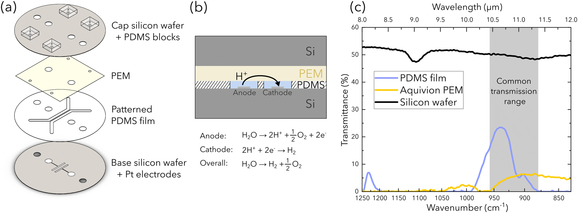 | ||
| Fig. 1 Schematic of the microfluidic PEM electrolyzer: (a) exploded view of the electrolyzer assembly, (b) section view showing the path of proton transport. (c) The IR transmission of each material used to fabricate the chip. Light transmits through all materials for wavenumbers from 880 cm−1 to 960 cm−1 (10.4 μm to 11.3 μm wavelengths). | ||
The chip is comprised of four layers assembled in a sandwich stack as shown in Fig. 1a. The base layer is a double-side polished silicon wafer with two sputter-coated electrodes that are deposited with titanium adhesion layers (∼60 nm thickness), then subsequently with platinum (∼300 nm thickness). The active area of each electrode is 0.08 cm2 (1 cm length × 0.08 cm width) and the space between electrodes is 1.2 mm. The second layer is a PDMS film with the microfluidic channels and electrode ports removed via a plotter cutter (Graphtec). The removed features are open to the top and bottom surfaces of the PDMS film such that the channel thickness is the same as the thickness of the PDMS film (38 μm). The third layer is the PEM that caps the patterned PDMS film. The final layer is another double-side polished silicon wafer with holes for electrode and tubing connections. The distance between the channels is 500 μm and each channel is 1.8 mm in width, 15 mm in length, and 38 μm in height. With this configuration, the protons that are produced at the anode will transfer from the bottom of the channels, to and then across the PEM capping the channels, down to the cathode (Fig. 1(b)).
The chip assembly procedure requires four-steps. First, the PDMS film is adhered to the base silicon wafer. Isopropanol is used to swell the PDMS film, which reduces the friction between the PDMS film and bottom silicon wafer, simplifying alignment between the channels on the PDMS film and the electrodes on the silicon wafer. After alignment, these components are inserted into a degassing chamber for 30 min to create adhesion between these two layers. Additionally, the degassing process removes any remaining isopropanol in the PDMS film or bubbles between the PDMS film and silicon wafer. Second, the PEM is adhered to the cap silicon wafer. The PEM is pre-swelled with a perfluorinated resin solution (Nafion 1100 W resin, Sigma-Aldrich), and is then firmly pressed for adhesion to the cap silicon wafer. PEM swelling/shrinkage is particularly challenging design constraint for the fabrication of this device, as excessive membrane swelling/shrinking can introduce delamination sites that cause leaks in the chip. The resin solution is used as the wetting agent to improve adhesion between the PEM and the silicon wafer, and to reduce the effects of membrane swelling/shrinkage that leads to the delamination of these layers. The PEM is then air-dried before cutting around the holes in the cap silicon wafer to create the electrode and tubing connections. Both the wafer-PDMS and PEM-wafer subassemblies are then inserted into an oven set to 65 °C overnight. Third, each subassembly is chemically bonded together through the following method prepared by Pham and Barz.28 Specifically, a 4.0 wt% aqueous solution of vinyltriethoxysilane (VTES) in ethanol containing 10 vol% water is prepared and stirred for 1 h at room temperature to create silanol groups. The PDMS surface is air plasma treated, then immersed in the VTES solution for 2 min to allow silanes to migrate to the PDMS surface. The PDMS is then air dried and heated at 100 °C for 15 min to graft the silanes to the PDMS through siloxane linkages. Towards the end of the 15 min PDMS heating step, the PEM is prepared with air plasma treatment. The plasma-treated surface of the PEM is firmly pressed onto the PDMS surface between two acrylic plates, and is then inserted into the oven set to 65 °C to create a chemical bond between the silane-grafted PDMS surface and the PEM. Finally, air plasma treatment is used again to attach four PDMS blocks with punched-holes to the cap silicon wafer of the chip for tubing ports, and then the completed chip is inserted into an oven set to 65 °C overnight.
Experimental procedure
The PEM water content is evaluated in the chip for a range of varied operating conditions while IR spectra are concurrently acquired. Specifically, the chip is operated for three temperature conditions (20°C, 40 °C, and 60 °C) to observe the effect on the PEM water content, and for two flow rate conditions (20 μL min−1 and 100 μL min−1) which are intentionally selected to observe the relationship between PEM water content and the ohmic/mass transport failure mechanisms. A custom copper thermistor (ring with 35 mm inner diameter and 50.8 mm outer diameter, Captec) is developed to measure the temperature of the chip and to heat it through an externally connected PID temperature controller. The thermistor is inserted and compressed between the chip and an adapter plate. Dilute sulfuric acid (0.5 mol L−1) is supplied to the cell to perform water splitting under acidic conditions. While a parasitic reaction is known to occur between sulfuric acid and platinum, this reaction is only expected to occur at potentials lower than the equilibrium potential (Erev = 1.23 V at standard conditions).29 Reactants are delivered to the chip with a syringe pump (Cetoni Nemesys) at the prescribed flow rate for 5 min before applying current and throughout the experiment. The electrolyzer is operated under galvanostatic control from a potentiostat (BioLogic SP-300) beginning at open circuit voltage (OCV) and is increased in increments of 25 mA cm−2 until cell failure for each operating condition. Cell failure is defined at a cell potential of E > 5 V to avoid excessive damage to the microfluidic chip from the corrosive reaction environment. Each constant current is held for 20 min. Between each galvanostatic current density, electrochemical impedance spectroscopy (EIS) is performed through the staircase galvanostatic method in increasing 2.5 mA cm−2 current density steps.30 The full range of experimental conditions tested are shown in Table 1.| Flow rate Q (μL min−1) | Temperature T (°C) | Current density i (mA cm−2) |
|---|---|---|
| 20 | 20 | OCV, 25, 50, 75 |
| 40 | ||
| 60 | ||
| 100 | 20 | OCV, 25, 50, 75, 100, 125 |
| 40 | OCV, 25, 50, 75, 100, 125, 150, 175 | |
| 60 | OCV, 25, 50, 75, 100, 125, 150, 175, 200, 225 |
Synchrotron FTIR spectroscopy
Experiments are performed with the IR beam positioned between the two channels of the electrolyzer (Fig. 2). The experiment is performed using the Bruker IFS125HR spectrometer at the far-infrared beamline at the Canadian Light Source in Saskatoon, Canada (Fig. 2a). IR light is extracted from one of the bending magnets of the synchrotron using a split mirror and is directed to the entrance aperture (set to 2 mm) of a Bruker IFS125HR spectrometer equipped with a KBr beamsplitter via a series of optic elements. Optics within the sample compartment of the spectrometer collimate the beam and direct it through a diamond window to a Cassegrain objective, which focus the beam to a 90 μm spot on the electrolyzer (Fig. 2b–d). Light that is transmitted by the electrolyzer is collected by the second objective and is recollimated. Finally the light is focused into a detector using a gain of 500 (Ge:Cu element with a range of 335–1300 cm−1 wavenumbers or 7.69–30 μm wavelengths, QMC Instruments).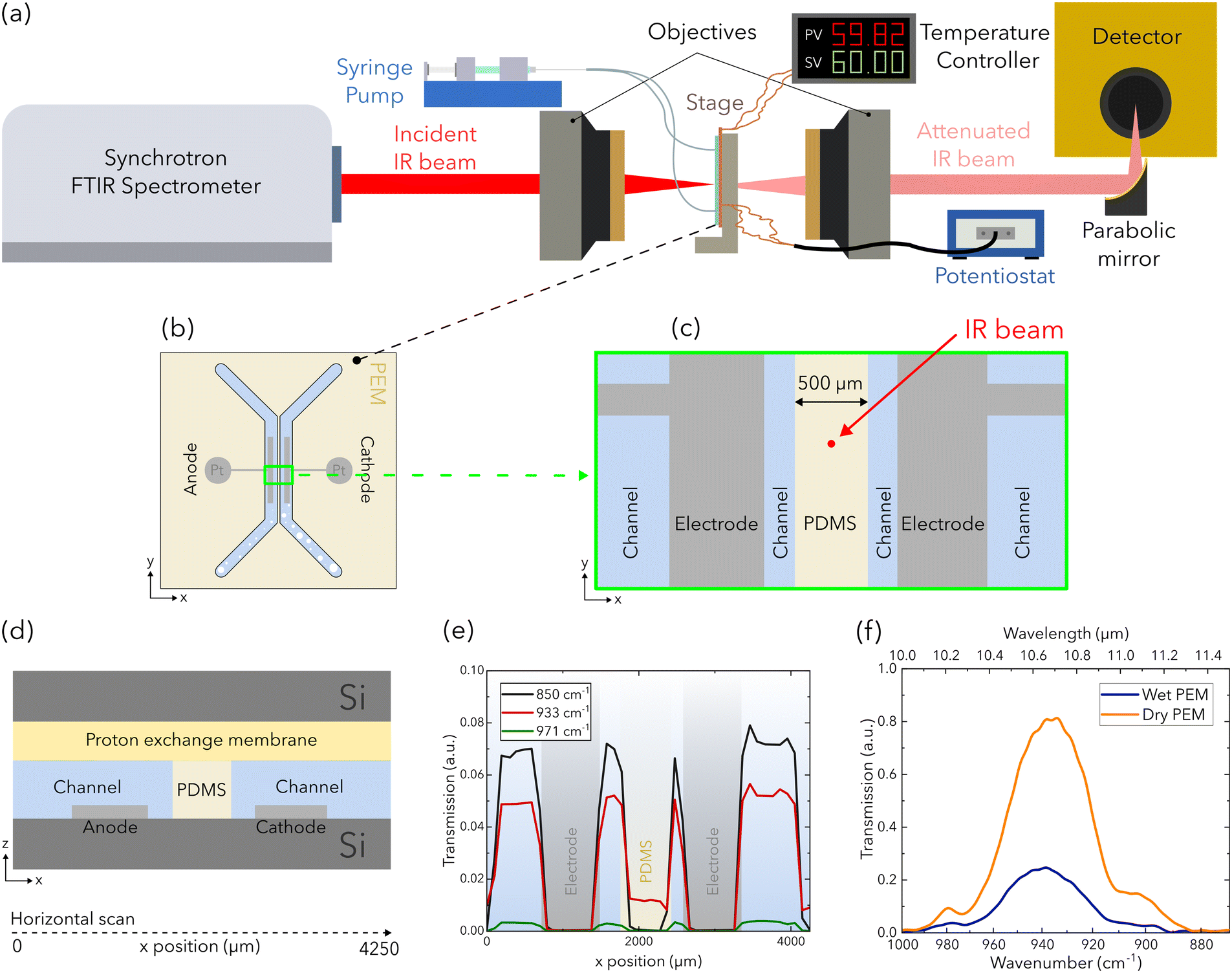 | ||
| Fig. 2 (a) Schematic of the experimental setup for infrared spectroscopy used at the synchrotron facility and (b) a schematic of the electrolyzer. Horizontal scans across both channels are performed with schematics of the (c) beam position and (d) a rotated view shown. (e) The corresponding transmissions of three wavenumbers near the common transmission range of each attenuating material are evaluated to position the beam. Centered on the PDMS strip, the attenuated IR beam produces (f) higher transmissions for the PEM when dry compared to wet. | ||
Due to the absence of any beam-alignment features in the microfluidic PEM electrolyzer, each feature of the chip had to be manually identified using individually acquired IR spectra. The chip was aligned to the beam, and then a series of horizontal scans across the chip were acquired using a monochromatic beam. The correspondingly acquired scans are presented at wavenumbers of 850 cm−1 (11.76 μm), 933 cm−1 (10.72 μm), and 971 cm−1 (10.30 μm) in Fig. 2e, where the transmission of each component is labeled. At the beam position between the channels as shown in Fig. 2c, the beam is only attenuated by the PEM, the PDMS film, and each silicon wafer. As a result, the change in beam attenuation can be attributed to water content change in the PEM and PDMS film over the experiment duration (Fig. 2f). For each temperature and flow rate condition, IR spectra are acquired for the final 120 s of OCV and at each constant current to allow stabilization of the potential response. Each IR spectrum is an average of 300 measurements acquired with a spectral resolution of 4 cm−1.
PEM water content
The acquired IR spectra are processed through the Beer Lambert law to determine the change in membrane water content from a reference state. Here, the IR spectrum acquired during OCV is used as the reference hydrated state. The Beer Lambert law is described through the following equation: | (1) |
 ) over wavelengths surrounding the IR transmission peak of interest (10.4–10.9 μm wavelengths, ESI†). The following relation converts
  to the percent change in water saturation (ΔS):
 | (2) |
3 Results and discussion
The electrochemical performance of the chip is monitored to examine the performance of the PEM during operation. Polarization curves for all operating conditions are presented in Fig. 3a, where each point on the polarization curve is averaged from the final 120 s of constant current operation. Each flow rate is chosen to target either ohmic or mass transport dominated overpotential. Specifically, the lower flow rate conditions (20 μL min−1) are chosen for mass transport dominated overpotential and exhibit exponential increases in the potential followed immediately by cell failure. This is confirmed by each lower flow rate condition failing after an applied current density of 75 mA cm−2. In contrast, the higher flow rate conditions (100 μL min−1) are chosen to target ohmic dominated overpotentials. Considering the polarization curves with the higher flow rate, a linear trend is observed for each temperature condition, confirming ohmic dominated overpotentials. Additionally, higher temperatures enable higher current density operation and exhibit reduced slopes (Fig. 3a), indicating either reduced ohmic overpotentials or improved reaction kinetics.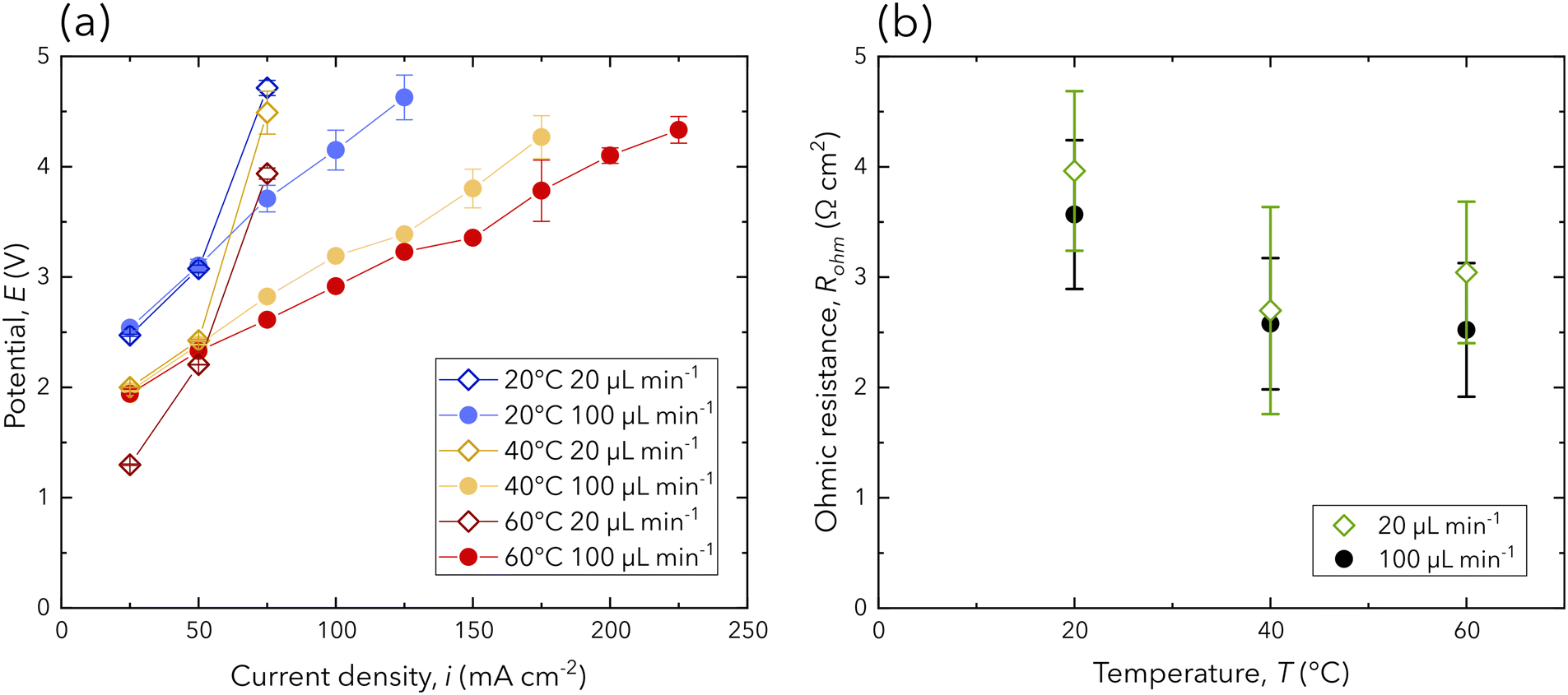 | ||
| Fig. 3 (a) The polarization curve of all experimental conditions, where each point is presented as the average potential from the final 120 s of galvanostatic operation. (b) The ohmic resistance averaged over each current density from staircase galvanostatic EIS. Individual ohmic resistance values presented in (b) can be found in the ESI.† Error bars are reported as the standard deviation. | ||
Given the novel design presented in this work, a comparison of the electrochemical performance to similar designs and industrial grade PEM electrolyzers needs to be evaluated to assess its viability. The ohmic resistance of the operating chip is extracted through a combination of EIS and fitting the equivalent electrical circuit used by Chevalier et al. (ESI†).31Fig. 3b shows the ohmic resistance for each experimental condition, which is averaged over each current density from staircase galvano EIS. While this design excels in its transparency in the IR domain bordering mid- and far-IR, the ohmic resistance is an order of magnitude higher than conventional electrolyzer and fuel cell stacks.11,17 Additionally, ohmic resistance measurements are highly unstable due to the chip's high sensitivity to gas formation, residence, and removal at the small active area (0.08 cm2). The high ohmic resistance and instability are due to the large path of ion transport. Ions must traverse from the anode through 38 μm of 0.5 mol L−1 sulfuric acid to the PEM, through it (inter-electrode distance of 1.2 mm), then back through the sulfuric acid to the cathode. Nevertheless, the chip is able to achieve competitive current density operation (>25 mA cm−2 at 2.5 V) with other chips using similar designs (lit.,26,27 17.5 mA cm−2 at 2.5 V).
The PEM hydration in the operating chip is quantified and compared to the respective potential response at each operating condition. The PEM hydration is expressed as change in water saturation from the reference state (OCV), as calculated in eqn (2). In Fig. 4a, the change in water saturation for each current density at a flow rate of 20 μL min−1 is shown, where mass transport overpotential is the cause of cell failure. At this flow rate, the PEM water content shows insignificant changes until the highest achieved current density (75 mA cm−2), when a reduction in the membrane water content occurs. This behavior is observed for each temperature condition with the largest decrease of −0.57% in water saturation at cell failure can be interpreted as membrane drying. Specifically, at the lower flow rate, product gas is less likely to be removed from the channel, drying the membrane and increasing mass transport overpotentials that induce cell failure. This behavior is confirmed in the literature using X-ray and neutron based techniques,16,17,32 and we provide further confirmation as the first using FTIR spectroscopy to discriminate the cause of cell failure based on the hydration of the PEM.
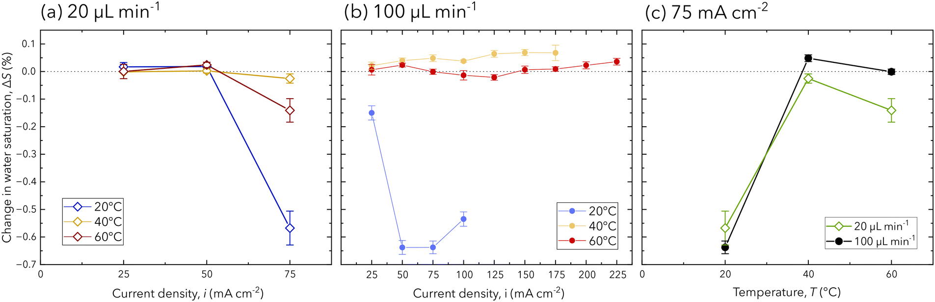 | ||
| Fig. 4 The change in PEM water saturation for each operating condition at a flow rate of (a) 20 μL min−1, (b) 100 μL min−1, and (c) for both flow rates and at a current density of 75 mA cm−2. Error bars are reported as the standard deviation for each measurement in the cropped IR spectrum (ESI†). | ||
At a flow rate of 100 μL min−1, the change in PEM water saturation shows both increases and decreases, for which no concurrent changes in the electrochemical performance (Fig. 3a) are observed. Comparable membrane drying to the low flow rate condition is observed to occur at 20 °C for current densities from 50 mA cm−2 to 100 mA cm−2; however, the higher flow rate of 100 μL min−1 is able to sustain electrochemical performance up to a failing current density of 125 mA cm−2. This behavior is expected, as the higher flow rate is able to provide sufficient reactant delivery and product removal, enabling improved current density operation that is dominated by ohmic losses. However, at temperatures of 40 °C and 60 °C, membrane drying is not observed, and changes in the PEM water saturation are within 0.1% for all current densities. The difference in measurements across all temperature conditions at 100 μL min−1 is attributed to the nature of FTIR spectroscopy, as the area for characterization is limited to the 90 μm beam spot size.
For both flow rates, the change in membrane water saturation is significantly lower for higher temperatures. In Fig. 4b, the relationship between the change in water saturation and temperature is presented for a current density of 75 mA cm−2, for which the largest reductions in the membrane water content are observed at 20 °C. At higher temperatures (40 °C and 60 °C), all experimental conditions (flow rate and current densities) show changes in membrane water content within −0.2% to 0.1%, which is attributed to the PEM's higher water uptake for higher temperatures. This is supported by the literature, which reports higher temperatures in PEMs being associated with higher electro-osmotic drag coefficients, water uptake, and protonic conductivity.3,5,15,33 Additionally, further increases in membrane hydration from its reference state do not occur, despite the performance increase from 40 °C to 60 °C (Fig. 3a). Therefore, the performance increase is attributed to improved ohmic performance or reaction kinetics at higher temperatures.
4 Conclusions
Here, the first microfluidic PEM electrolyzer that is semi-transparent in the IR domain (bordering mid- and far-IR) is developed as a platform for characterizing the operando PEM water content. Two modes of electrochemical failure are explored to observe the membrane water content over a range of applied temperatures. The lower flow rate drives mass transport-dominated cell failure up to current densities of 75 mA cm−2, for which a reduction in membrane water content occurs, while the higher flow rate drives ohmic-dominated cell failure and can sustain improved current densities of up to 225 mA cm−2. The electrochemical performance of this chip is comparable to similar architectures presented in the literature but is specifically designed to be semi-transparent in IR, enabling the membrane water content measurements. While the ohmic resistance of the chip is an order of magnitude higher than a conventional full-scale fuel cell or electrolyzer, this can be reduced by optimizing the large path of ion transport.For the first time, membrane hydration is characterized via operando synchrotron FTIR spectroscopy, where the change in water saturation is measured while current is applied. A reduction in water saturation is observed immediately before cell failure for the lower flow rate conditions (largest reduction of ΔS is −0.57%), demonstrating membrane drying with cell failure. Furthermore, the change in water saturation and temperature was observed for both flow rates, where the improved water uptake with higher temperatures (i.e. 40 °C and 60 °C) causes the least variation in the membrane water content (ranging from −0.2% to 0.1%). These results validate our methods for using FTIR spectroscopy to determine how membrane hydration affects improved electrochemical performance or cell failure.
This study acts as a first step to evaluating the PEM in an operating electrolyzer using IR techniques. Further investigation focused on the impact of this cell design (specifically the chemical bonding method) on membrane performance may further clarify internal membrane mechanisms. Additionally, the insights gained from operando FTIR spectroscopy in this configuration is limited to local information at the IR beam's position on the chip. Coupling the microfluidic chip presented here with a suitable IR source and camera will allow visualization of global water transport through the PEM. If the IR camera is also capable of thermography, it can also be used to capture any sites of membrane cracking/deformation that may occur during operation. These imaging techniques may unveil water gradients across the PEM, allowing us to clarify how operating conditions affect electro-osmotic drag and protonic conductivity. The insights gained by coupling operando IR techniques with these devices are invaluable to the field for elucidating real-time membrane behaviors in these devices.
Author contributions
K. K. and S. C. contributed to the research project conceptualization. K. K. designed the microfluidic chip. K. K., M. G., and G. C. contributed to the electrolyzer fabrication. D. M. performed the metal deposition onto the base silicon wafer. K. K., M. G., B. B., and S. C. performed calibrations and experiments at the synchrotron facility. S. C. and J. L. B. supervised the research project. K. K. wrote the original draft of the manuscript. All authors were involved in the reviewing and editing of the manuscript.Conflicts of interest
There are no conflicts of interest to declare.Acknowledgements
Part or all of the research described in this paper was performed at the Canadian Light Source, a national research facility of the University of Saskatchewan, which is supported by the Canada Foundation for Innovation (CFI), the Natural Sciences and Engineering Research Council (NSERC), the National Research Council (NRC), the Canadian Institutes of Health Research (CIHR), the Government of Saskatchewan, and the University of Saskatchewan. S. C. and M. G. gratefully acknowledge the French National Research Agency (ANR) for its support through project I2MPAC, grant number ANR-20-CE05-0018-01.Notes and references
- A. S. Gago, J. Bürkle, P. Lettenmeier, T. Morawietz, M. Handl, R. Hiesgen, F. Burggraf, P. A. Valles Beltran and K. A. Friedrich, ECS Meet. Abstr., 2018, vol. MA2018-02, p. 1607 Search PubMed.
- M. Carmo, D. L. Fritz, J. Mergel and D. Stolten, Int. J. Hydrogen Energy, 2013, 38, 4901–4934 CrossRef CAS.
- A. Z. Weber, R. L. Borup, R. M. Darling, P. K. Das, T. J. Dursch, W. Gu, D. Harvey, A. Kusoglu, S. Litster, M. M. Mench, R. Mukundan, J. P. Owejan, J. G. Pharoah, M. Secanell and I. V. Zenyuk, J. Electrochem. Soc., 2014, 161, F1254–F1299 CrossRef.
- A. Z. Weber and J. Newman, J. Electrochem. Soc., 2003, 150, A1008 CrossRef CAS.
- S. Ge, B. Yi and P. Ming, J. Electrochem. Soc., 2006, 153, A1443 CrossRef CAS.
- G. Karimi and X. Li, J. Power Sources, 2005, 140, 1–11 CrossRef CAS.
- Y. H. Park and J. A. Caton, Int. J. Hydrogen Energy, 2008, 33, 7513–7520 CrossRef CAS.
- H. S. Shin and B. S. Oh, Int. J. Hydrogen Energy, 2020, 45, 56–63 CrossRef CAS.
- M. Chandesris, V. Médeau, N. Guillet, S. Chelghoum, D. Thoby and F. Fouda-Onana, Int. J. Hydrogen Energy, 2015, 40, 1353–1366 CrossRef CAS.
- F. M. Sapountzi, M. Lavorenti, W. Vrijburg, S. Dimitriadou, B. Tyburska-Pueschel, P. Thüne, H. Niemantsverdriet, T. V. Pfeiffer and M. N. Tsampas, Catalysts, 2022, 12, 1–13 CrossRef.
- M. Watanabe, H. Uchida, Y. Seki, M. Emori and P. Stonehart, J. Electrochem. Soc., 1996, 143, 3847–3852 CrossRef CAS.
- L. Ma, S. Sui and Y. Zhai, Int. J. Hydrogen Energy, 2009, 34, 678–684 CrossRef CAS.
- T. A. Zawodzinski, J. Davey, J. Valerio and S. Gottesfeld, Electrochim. Acta, 1995, 40, 297–302 CrossRef CAS.
- T. A. Zawodzinski, C. Derouin, S. Radzinski, R. J. Sherman, V. T. Smith, T. E. Springer and S. Gottesfeld, J. Electrochem. Soc., 1993, 140, 1041–1047 CrossRef CAS.
- H. Ito, T. Maeda, A. Nakano and H. Takenaka, Int. J. Hydrogen Energy, 2011, 36, 10527–10540 CrossRef CAS.
- O. Panchenko, E. Borgardt, W. Zwaygardt, F. J. Hackemüller, M. Bram, N. Kardjilov, T. Arlt, I. Manke, M. Müller, D. Stolten and W. Lehnert, J. Power Sources, 2018, 390, 108–115 CrossRef CAS.
- N. Ge, R. Banerjee, D. Muirhead, J. Lee, H. Liu, P. Shrestha, A. K. C. Wong, J. Jankovic, M. Tam, D. Susac, J. Stumper and A. Bazylak, J. Power Sources, 2019, 422, 163–174 CrossRef CAS.
- J. Roth, J. Eller and F. N. Büchi, J. Electrochem. Soc., 2012, 159, F449–F455 CrossRef CAS.
- J. Eller and F. N. Büchi, J. Synchrotron Radiat., 2014, 21, 82–88 CrossRef CAS PubMed.
- G. M. Hale and M. R. Querry, Appl. Opt., 1973, 12, 555 CrossRef CAS PubMed.
- M. N. Polyanskiy, Refractive index database, https://refractiveindex.info, (accessed 29 June 2023).
- E. Kjeang, R. Michel, D. A. Harrington, N. Djilali and D. Sinton, J. Am. Chem. Soc., 2008, 130, 4000–4006 CrossRef CAS PubMed.
- D. V. Esposito, Joule, 2017, 1, 651–658 CrossRef CAS.
- J. W. Lee and E. Kjeang, Int. J. Hydrogen Energy, 2012, 37, 9359–9367 CrossRef CAS.
- Y. A. Song, C. Batista, R. Sarpeshkar and J. Han, J. Power Sources, 2008, 183, 674–677 CrossRef CAS.
- M. A. Modestino, C. A. Diaz-Botia, S. Haussener, R. Gomez-Sjoberg, J. W. Ager and R. A. Segalman, Phys. Chem. Chem. Phys., 2013, 15, 7050–7054 RSC.
- M. A. Modestino, M. Dumortier, S. M. Hosseini Hashemi, S. Haussener, C. Moser and D. Psaltis, Lab Chip, 2015, 15, 2287–2296 RSC.
- M. H. Pham and D. P. J. Barz, J. Membr. Sci., 2017, 537, 310–314 CrossRef CAS.
- F. Kodera, Y. Kuwahara, A. Nakazawa and M. Umeda, J. Power Sources, 2007, 172, 698–703 CrossRef CAS.
- R. Attias, B. Dlugatch, M. S. Chae, Y. Goffer and D. Aurbach, Electrochem. Commun., 2021, 124, 106952 CrossRef CAS.
- S. Chevalier, N. Ge, J. Lee, M. G. George, H. Liu, P. Shrestha, D. Muirhead, N. Lavielle, B. D. Hatton and A. Bazylak, J. Power Sources, 2017, 352, 281–290 CrossRef CAS.
- C. Immerz, B. Bensmann, P. Trinke, M. Suermann and R. Hanke-Rauschenbach, J. Electrochem. Soc., 2018, 165, F1292–F1299 CrossRef CAS.
- T. A. Zawodzinski, T. E. Springer, J. Davey, R. Jestel, C. Lopez, J. Valerio and S. Gottesfeld, J. Electrochem. Soc., 1993, 140, 1981–1985 CrossRef CAS.
Footnote |
| † Electronic supplementary information (ESI) available. See DOI: https://doi.org/10.1039/d3lc00380a |
| This journal is © The Royal Society of Chemistry 2023 |