
 Open Access Article
 This Open Access Article is licensed under a Creative Commons Attribution-Non Commercial 3.0 Unported Licence
Protruding cantilever microelectrode array to monitor the inner electrical activity of cerebral organoids†
Oramany
Phouphetlinthong‡
 ac,
Emma
Partiot‡
bc,
Corentin
Bernou
bc,
Audrey
Sebban
ac,
Raphael
Gaudin§
*bc and
Benoit
Charlot§
*ac
ac,
Emma
Partiot‡
bc,
Corentin
Bernou
bc,
Audrey
Sebban
ac,
Raphael
Gaudin§
*bc and
Benoit
Charlot§
*ac
aIES, Institut d'Electronique et des Systèmes, UMR 5214 CNRS, Montpellier, France
bIRIM, Institut de Recherche en Infectiologie de Montpellier, UMR 9004 CNRS, Montpellier, France
cUniversity of Montpellier, Montpellier, France. E-mail: raphael.gaudin@irim.cnrs.fr; benoit.charlot@umontpellier.fr
First published on 17th July 2023
Abstract
Stem cell-derived cerebral organoids are artificially grown miniature organ-like structures mimicking embryonic brain architecture. They are composed of multiple neural cell types with 3D cell layer organization exhibiting local field potential. Measuring the extracellular electrical activity by means of conventional planar microelectrode arrays is particularly challenging due to the 3D architecture of organoids. In order to monitor the intra-organoid electrical activity of thick spheroid-shaped samples, we developed long protruding microelectrode arrays able to penetrate the inner regions of cerebral organoids to measure the local potential of neurons within the organoids. A new microfabrication process has been developed which, thanks to the relaxation of internal stresses of a stack of materials deposited over a sacrificial layer, allows one to build a protruding cantilever microelectrode array placed at the apex of beams which rise vertically, over two hundred microns. These slender beams inserted deeply into the organoids give access to the recording of local field potential from neurons buried inside the organoid. This novel device shall provide valuable tools to study neural functions in greater detail.
Introduction
Organoids1 are composed of multiple cell types from a given organ, exhibiting a self-organized three-dimensional architecture, and differentiated from stem cells. They originate either from embryos (human embryonic stem cells: hESCs) or from differentiated adult cells that are dedifferentiated through reprogramming (induced pluripotent stem cells: iPSCs). Stem cells are naïve and exhibit the unique ability to differentiate into virtually any kind of cell type in vitro, such as neurons, hepatocytes, intestinal cells, myoblasts, or airway epithelia. Although it started as the 2D differentiation of cell monolayers, the stem cell research field quickly started to grow the cells in 3D and direct cell differentiation not to a unique cell type, but rather a panel of cells coexisting within the same organ. As such, the term “organoid” was coined to refer to these 3D cell cultures containing various cell types and exhibiting complex, yet highly organized, architectures.The development of organoids mimicking an embryonic human brain cortex was initiated less than a decade ago,2 and since then tremendous efforts have been devoted to further characterize these systems. Moreover, cerebral organoids have been employed to investigate major conundrums in a wide range of fields.3,4 Besides the obvious importance of cerebral organoids to study neurodevelopment and disease modeling,5 the last couple of years highlighted that cerebral organoids can also provide unique access to functional studies in non-animal models through the measurement of local field potential.6–11
Cerebral organoids form a complex and organized 3D architecture of multiple cell types, including neural progenitor cells, astrocytes and post-mitotic neurons. As such, they are increasingly employed to model brain disorders, such as neuroinfection and neurodevelopmental diseases.12–17
This field has been growing very quickly, but the adaptation of existing microelectrode arrays,18 commonly used for the measurement of electrical activity from 2D neuron monolayers, does not suit the 3D structure of cerebral organoids. A major technical challenge to overcome is therefore to be able to record the large amount of electrical information buried into the inner part of cerebral organoids with high sensitivity.
Several studies employed calcium indicators to optically probe the calcium intakes in cells as a surrogate to measure electrical activity patterns in organoids;19,20 although this technique may be practical and efficient, it suffers from a lack of temporal resolution, complexity in measuring the fluorescence of the cells in 3D over large size samples and a possible bias due to phototoxicity inherent to the high power beam required for fluorophore excitation.
Planar microelectrode arrays (MEAs) are increasingly used for recording in parallel the electrical activity from many excitable cells,21 and they are now used in combination with microfluidics to monitor and stimulate reconstructed neuronal junctions22,23 even in multiwell devices.24 However, extracellular potentials are in the small-amplitude range of a few hundreds of microvolts and, as a general feature, their amplitude tends to become smaller the farther away is the recording electrode from the neuronal ensemble generating them;25 hence, a good electrical coupling between the recording electrode and the neuronal ensemble is highly desirable. When growing cerebral organoids on a planar MEA6,26,27 extracellular potential measurement is restricted to the cell layer on the surface (few tens of microns), which only provides a partial picture of the organoid network activity; further, superficial recording via planar MEA has proved somewhat difficult in terms of reproducibility, possibly because the majority of electrically active neurons populate the inner layers of the organoid. As a result, a systematic assessment of the electrical activity of brain organoids has been so far very challenging.
From a technological point of view, in vitro devices have been developed specifically either for 2D cultures of dissociated cells or for slices (planar MEA), or to measure electrical activities in the brain in vivo with the installation of implantable electrode arrays. Measuring the internal electrical activity of organoids takes place at an intermediate millimeter scale, between cells and organs, where for the moment there is no technical solution that has been widely adopted by the community. However, several solutions have been investigated in the literature28 to overcome this problem without a truly effective and reliable solution emerging.
A first approach was to use conventional planar MEAs and cut the organoids in half to expose the active cells directly on the electrode array.6 In a similar way to slicing, i.e. using a microtome, it is possible to obtain 0.5 mm organoid slices and apply them to the microelectrode array. It proved efficient in the past, but this approach necessarily comes with neuronal damage, loss of organoid integrity, and impaired neural network organization.
Another solution explored is the use of conical electrodes, originally developed by M. Heuschkel,29 for brain slices that were designed to penetrate deeper into the tissue than planar electrodes, up to 60 μm deep. While this technique is effective for slices, these electrodes are not sharp enough to penetrate deep into the interior of an organoid.
On a smaller scale, vertical nanoelectrode arrays30–33 or mushroom-shaped electrodes34 have been developed to monitor intracellular potential with the use of sharp nano-sized electrodes able to enter the intracellular compartment. However, these devices were designed to penetrate inside a cell, i.e. the tips rise a few microns above the surface and this distance is not sufficient to locate the sensitive area of the electrodes inside a spheroid which can be up to 5 mm in diameter.
Another possibility is to take advantage of the malleability of organoid tissues by growing them on a suspended mesh containing the electrode array.35,36 By growing the organoid for a few months, the cells will progressively deform around the mesh until the grid is embedded into the organoid. This technique is effective to measure the electrical activity inside organoids at the cost of a relative technological complexity of manufacturing and a long culture duration onto the mesh electrodes.
An interesting approach has been made by A. Soscia et al.37 to obtain vertically pointed and slender microelectrodes. The technique is based on flat fabrication of the electrodes on a deformable polyimide substrate. However, the technique for straightening the electrodes is done by hand, by bending the microbeam with a micromanipulator, which makes the process tedious and impossible to scale up.
A particular solution has been implemented by several labs,27,38–40 which consists in surrounding the spheroid with a deformable structure, also made on a polyimide substrate. These structures, folded around the spheroid, place microelectrodes on the outer surface of the organoid, an elegant method that cannot however record the inner electrical activity of organoids.
Finally, another technique that has been developed is the use of 3D microelectrode arrays,28,41 such as Utah array42,43 or Neuropixel,44 originally developed for in vivo implantation but can be used to probe electrical activities of organoids in vitro. Although the use of these devices in vivo benefits from the very great technological advance offered by these devices, the fact remains that they are poorly adapted in terms of size and specifications to the case of cerebral organoids.
In addition to passive microelectrode arrays, there are many developments based on CMOS technologies45–47 that integrate row and column transistors as well as decoders and amplifiers and thus allow the integration of a very large number of electrodes. In particular, the company 3Brain is developing protruding metallic microelectrode technology (4096 electrodes, 20 μm × 20 μm square section, 60–100 μm high) based on a CMOS sensor.46 Also some studies are done using high-density CMOS MEAs47,48 to decipher the electrical activity of cells in slices hundreds of microns away from the surface of the MEA. However, the very high integration of CMOS arrays, which offer high density with tens of thousands of small electrodes, is not really compatible with the establishment of a 3D network that allows potentials to be probed far from the surface. In addition, the use of a CMOS substrate, which is opaque to light, prohibits the use of transmission fluorescence techniques and forces the use of immersible lenses, which greatly complicates experiments.
In this paper we will present a microfabrication technique (Fig. 1 and 2) that allows us to produce an array of sharp, pointed microelectrodes (called csMEA for curvy and spiky MEA) that stand several hundred microns from the surface and are able to penetrate deep into the tissue (Fig. 2 and 4) of a hESC-derived cerebral organoid to sensitively record local field potentials, opening new avenues to investigate neural functions from within. The paper will focus on the design and microfabrication techniques we employed to build such devices with a demonstration of its effectiveness to record the extracellular electrical activity of a cerebral organoid impaled on it.
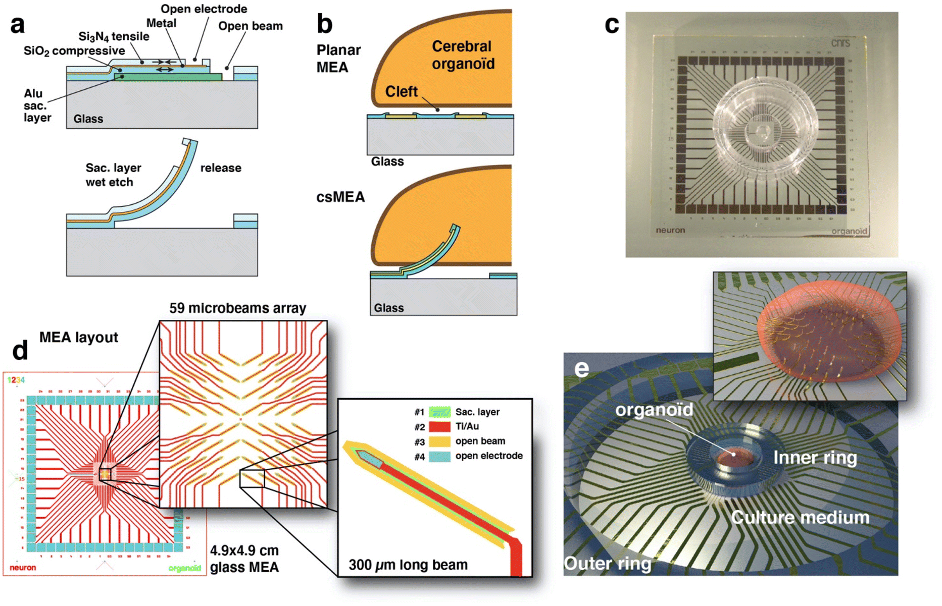 | ||
| Fig. 1 (a) Technological cross section of the MEA (not to scale, thicknesses have been exaggerated for the schematic) showing the layer stack before and after sacrificial layer etching and beam displacement. (b) Schematic of the placement of a cerebral organoid on top of a conventional planar MEA showing the cleft layer between cells and electrodes and a schematic representation of an organoid inserted on a spiky microelectrode. (c) Photograph of the functional MEA showing the PDMS inner and outer rings. (d) Layout of the MEA showing the 4 different levels corresponding to actual photolithography masks; inset: close-up view of the 59 microelectrode arrangement and a close-up view of one beam. (e) 3D schematic representation of a cerebral organoid impaled on the MEA and kept in place with the PDMS ring. | ||
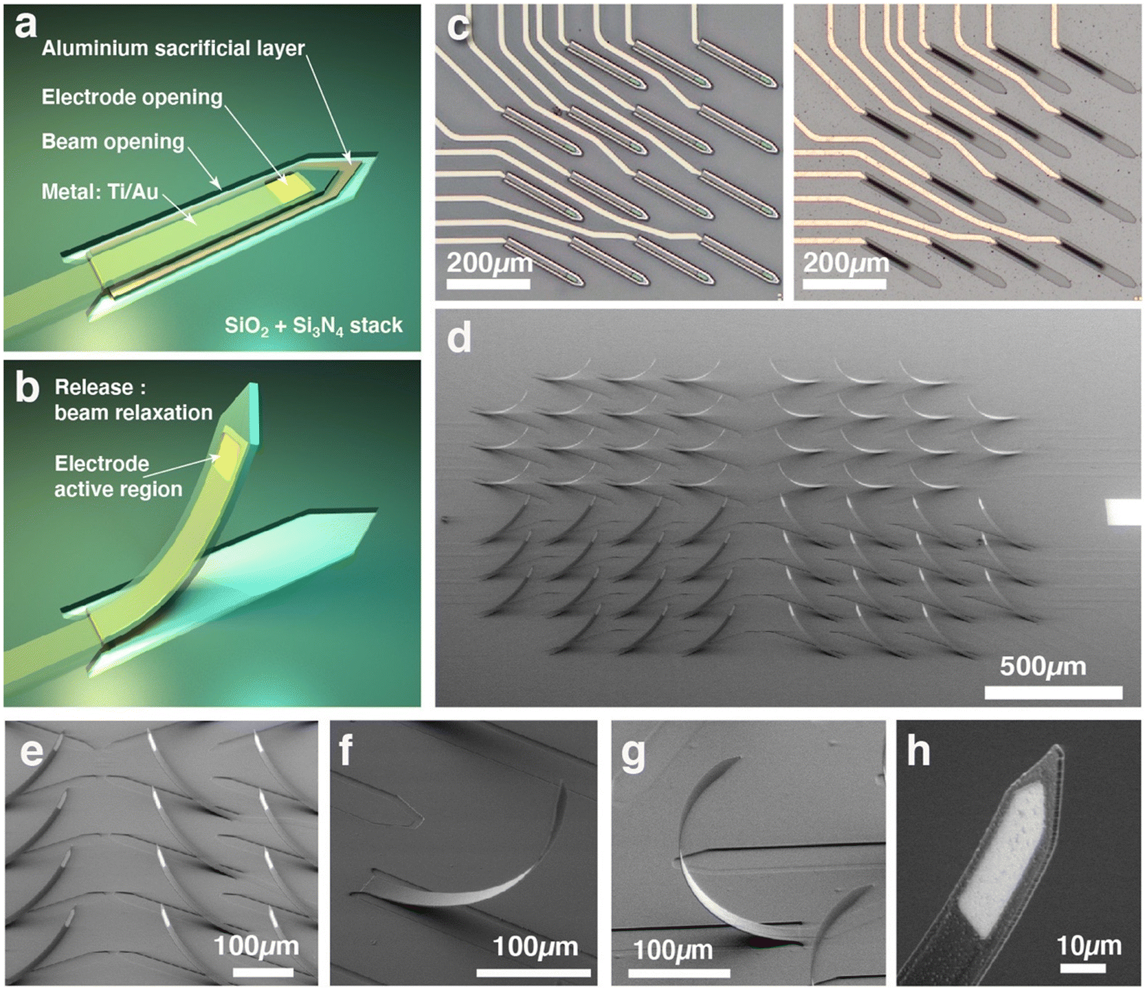 | ||
| Fig. 2 Schematic of the principle of microfabrication of the spiky electrodes; the deposition and patterning of the materials is made on the surface of a glass substrate over an aluminum sacrificial layer (a). Once etched, the beam sporting one electrode relaxes its internal stress and straightens (b). (c) Optical photograph of the array of microbeams before and after beam release. (d) SEM image of the whole array and (e) detail of the beams showing the active region on each beam. Example of correct (f) and over (g) curvature of a beam. (h) Detail of the active region at the end of one cantilever. | ||
Results and discussion
MEA design
The conception and design of our system had to face several constraints. Cantilevers that form the pointed electrodes are manufactured horizontally, so they occupy a large surface area, and as the electrical routing is done on a single level of metal, the layout of the beams must allow for the passage of the associated electrode routing wires. Furthermore, the electrodes must be placed on a limited surface area that corresponds to the average diameter of an organoid, i.e. approximately 3 mm. The organization we have chosen therefore consists of four quadrants of 15 electrodes, each one oriented toward the center and tilted at an angle of 30° (Fig. 1(c) and 2(d)). This configuration has been made in order to leave some room for the routing passing in between the beams (Fig. 1(c)) and also to generate an array of tilted beams, allowing the organoid to be impaled on it without sliding on one side. The pitch between electrode sites is 240 μm and a shift has been introduced between four quadrants in order to consider the change of position of the electrode with the release of the beam. The final result is a square array of vertical electrodes with a regular pitch.The beams are 320 μm long and 20 μm wide and are designed with a sharp end in order to easily penetrate tissues. A rounded shape is included at the base of each beam in order to minimize the stress at the location of maximum stress. The electrode site is located near the tip apex (Fig. 1(d) and 2(b and h)) with a 12 μm wide routing layer going along the beam and connecting one pad, expanding its width along the way to the pad to minimize the electrical resistance. The electrode site area is 470 μm2, and the impedance shows a value around 500 kΩ at 1 kHz for a 500 mV peak-to-peak signal measured in saline buffer (PBS 1×), as shown in Fig. ESI2.† This impedance can be lowered to increase the signal-to-noise ratio by growing porous gold49 or growing PEDOT:PSS50 at the electrode active sites.
Microfabrication of the cantilever MEA
The technique we propose here produces an array of microelectrodes that are sufficiently sharp and slender to penetrate directly into the organoid to operate the measurement of local field potentials several hundred microns away from the organoid surface. For this purpose, we have developed a relatively straightforward microfabrication process based on standard techniques and materials. The device is made on transparent glass substrates (Fig. 1(c)), and not on silicon, which allows the organoid to be also monitored by confocal fluorescence microscopy or to couple electrical recording and optical calcium imaging.23,51Fabricating an out-of-plane microstructure using photolithography and material deposition/etching techniques is not easy since typical deposited layer thicknesses rarely exceed one micrometer. Deep reactive ion etching techniques allow for high depth (>100 μm) and large aspect ratios but are limited to opaque silicon and at the cost of high complexity and cost of the microfabrication process. The process presented here is then based on planar fabrication of microbeams on a sacrificial layer which, once removed by wet etching, will straighten to an upward facing shape. The microfabrication process is an adaptation of the standard process we developed for fabricating planar MEA.22,23 In order to obtain vertical tips several hundred microns high, we used the bimetal strip effect, although we did not use metals but silicon compounds. This mechanical effect allows us to obtain straightened structures from flat material layers. We therefore took advantage of the internal stresses of materials (silicon oxide and nitride) deposited by plasma enhanced chemical vapor deposition (PECVD). Indeed, these materials have different internal stresses, compressive for silicon oxide (measured at −284 MPa) and tensile for silicon nitride (measured at +246 MPa). By depositing a sandwich of silicon nitride on top of silicon dioxide (Fig. 1(a and b) and 2(a)) we have formed a structure that has internal stresses, resulting in a push–pull effect when attached to the substrate and that will straighten when released by the etching of the sacrificial aluminum layer below thanks to the relaxation of internal stresses. The result, visible in Fig. 2, is a beam that is twisted to the vertical direction, presenting a circular deformed shape with a curvature radius of about 200 μm.
The thickness of the material stack (typically 500–1200 nm for each layer) influences the deformation of released cantilevers and hence the angle at the apex that we want to be as close as possible to 90°. The relation of the curvature radius as a function of cantilever thickness will be discussed in the next section. The metal layer, consisting of 150 nm gold deposited on a 20 nm titanium adhesion layer, which is used for the active part of the electrode and the electrical routing, is placed between the oxide layer and the nitride layer. The aim of this is to locate the metal layer close to the neutral fiber of the beam in order to minimize the deformation of the metal so as not to cause cracks and also to avoid disturbing the stress relaxation that causes the beam to deform.
Beam release
Microfabrication results are shown in Fig. 2, where we can observe the shape of the beams after release. The first thing we observe is that the beams do indeed stand upright and that the stress relaxation in the stacking of the layers does produce a deformation of the beam in the vertical direction. We can notice the almost circular shape of the beams and the angle of the apex approaching 90° (Fig. 2(f)) versus the surface plane (Fig. ESI3†). Different ratios of SiO2/Si3N4 film thicknesses have been tested with different results, from a 70° (Fig. 2(e)) angle to more than 110° (Fig. 2(g)).The beam release steps and especially the drying of the MEA after the final step, although prone to break some beams, can give 100% yield if special care is taken during nitrogen gun drying and the use of low-pressure gas flux. Capillary effects caused by liquid surface tension can induce beam deformation and sticking during dewetting and drying; that is why we immerse devices in a lower surface tension liquid such as isopropyl alcohol before N2 drying. As can be observed in Fig. 3, cantilevers after release show the same circular shape that does not depend on their length, which will be discussed in the next section.
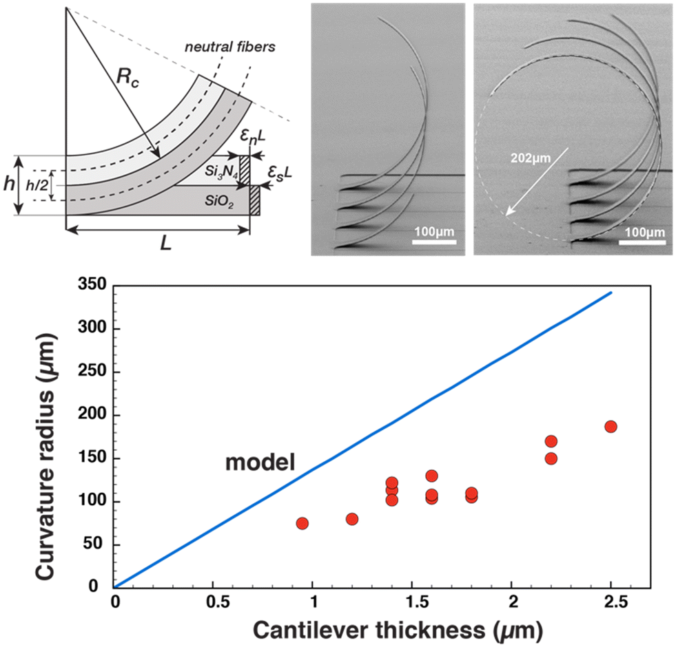 | ||
| Fig. 3 (Top) Schematic of the analytical mechanical problem and SEM pictures of relaxed cantilever beams of increasing lengths (200 to 800 μm by steps of 100 μm, width 40 μm) showing the circular deformed shape as well as a measurement of the radius of curvature. (Bottom) Curvature radius vs. cantilever thickness, comparison between analytical model (blue line) and measurement (red dots). | ||
Mechanical modeling
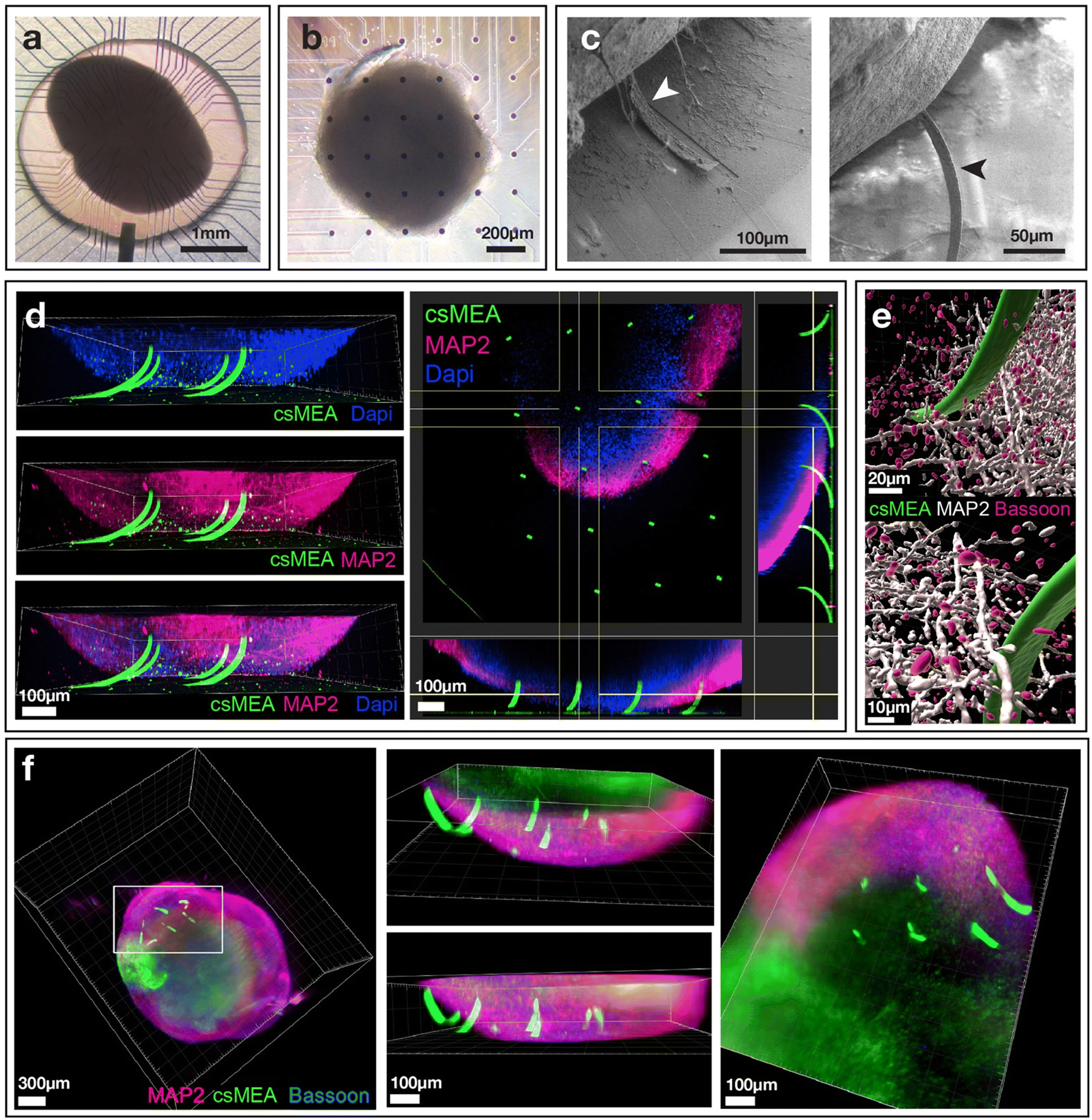 | ||
| Fig. 4 Characterization of hESC-derived cortical organoids and their csMEA impalement. (a) Transmission light microscopy of a cortical organoid placed on the center of a cantilever MEA held in place with a 3 mm PDMS ring and (b) of a cortical organoid placed on top of a conical shaped MEA. (c) Scanning electron microscopy of a cerebral organoid impaled onto a cantilever MEA after desiccation. (d) Confocal image acquisition of organoid impaled onto the csMEA. Green: PLL-FITC marks the cantilevers, pink MAP2 marks the neurons, blue DAPI marks cell nuclei. (e) Confocal imaging of cells in the vicinity of a cantilever; green PLL-FITC marks the cantilevers, white MAP2 marks the neurons and pink Bassoon marks the synapses. (f) Light sheet imaging of organoids detached from the csMEA but still with the cantilevers inside. | ||
We find that our problem is close to the bimetallic strip case that has been derived by Timoshenko.52 The main differences lie in the fact that the dilatation of the strip is caused by internal stresses rather than thermal dilatation of metals and that we have a push–pull effect that is not present in the thermal bimetal model.
To start, we used Hooke's law to calculate the strain of a beam subjected to an internal stress
| σ = εE |
The expression of the radius of curvature as a function of internal stresses, Young's modulus and thickness of the beam can be obtained with some geometrical considerations, as depicted in Fig. 3. Let us consider two beams under compressive and tensile stresses, respectively, which will expand or contract according to their modulus of elasticity.
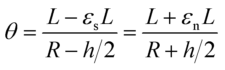
If we then consider that these two beams are attached without sliding to each other and that the deformation is a circle of radius Rc, as we observed experimentally, it is possible to say that the arc of the circle that describes them shows the same angle theta. Thus,
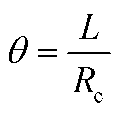
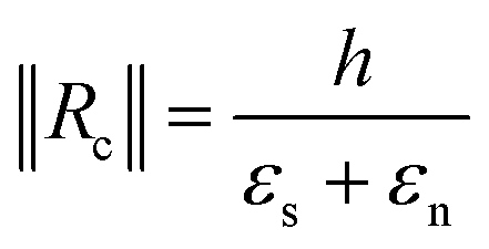
By developing this equation, we realize that the initial length of the beam L disappears and that we can isolate the radius of curvature Rc as a function of both the strains (εs and εn) and the height of the stack h:
Considering finally that the dilatations are very small, we can simplify the equation as:

By injecting the measured values of the mechanical stresses of the layers and by taking average values of Young's modulus for silicon dioxide and nitride (70 and 150 GPa, respectively) we obtain the line that is plotted in Fig. 4. The plot contains also the measurement of curvature radius made on cantilevers with different thicknesses and measured by SEM (Fig. ESI4†). We can observe that we have a linear variation of the curvature radius with the cantilever thickness and that it is lower than that computed with the analytical model.
Of course, this model is simplistic and does not only consider many mechanical effects such as the Poisson modulus, the effective distribution of stresses in the section of the beam, the presence of rounded sections at the base of cantilevers, and the thin layer of metal in between silicon dioxide and nitride layers but also relies on measurement of stresses with low precision and with Young's modulus values of PECVD deposited layers taken from the literature. However, it does account for both the observed circular shape of the cantilevers and the linear relation and the order of magnitude of the radius of curvature which is directly proportional to the total thickness of the composite cantilever. This allows us, at the time of cantilever fabrication, to adjust the total height of the deposited layers so that, for a given length of the beam defined by the photomask, the cantilever is pointed vertically, forming a quarter circle, so that the tip of the beam is normal to the surface and the organoid impales itself effectively on the cantilever electrode array.
To gain further insights into the spatial insertion of the beams into the organoids, confocal and light sheet microscopy analyses of cantilever-impaled organoids were performed. For this, cantilevers were tagged with PLL-FITC, allowing fluorescein to be bonded to the cantilevers through the attachment of polylysine on SiO2 and Si3N4 in order to be able to observe them with fluorescence microscopy. Three-dimensional observations clearly showed that the beams were inserted into the organoids (Fig. 4(d and f)). Depending on the position of the cantilevers in the array and especially their position in relation to the center of the spheroidal tissue, we can observe that some cantilevers are inserted by only about ten microns, placing the active zone of the electrodes within the first cell layers of the tissue, whereas others are inserted over more than a hundred microns, i.e. over more than half their nominal length (300 μm). We were also able to observe MAP2-expressing neurons as well as presynaptic structures in contact (or very close proximity) with the cantilever (Fig. 4(e)). These structures being critical for electrical signal propagation within the organoid, our data indicate that the electrodes would be able to readily record the electrical activity of neurons deep into the organoid.
Confocal microscope (Fig. 4(d and e)) and light sheet images (Fig. 4(f)) clearly show the insertion of the cantilevers inside the tissue, with some of the cantilevers penetrating more than two-thirds of their length. We also note that due to the rounded shape of the organoids, some cantilevers do not penetrate the tissue, especially those located on the edges of the organoid. Of note, despite the use of a light sheet microscope, the center of the organoid was mostly unstained, probably because our procedure did not allow deep penetration of the antibodies used for the staining.
Next, the impaled organoids on the cantilevers were observed with scanning electron microscopy (SEM). For SEM analysis, the organoids were used without any special treatment apart from fixation and drying. This lack of specific sample preparation resulted in the organoids losing water during drying and shrinking, finally losing volume. Because the organoids were impaled on the microbeams, this shrinkage tore the microbeams apart, which can be seen in Fig. 4(c). Although a specific treatment is required to maintain the integrity of the organoid for SEM imaging under vacuum, we were still able to observe the presence of the microbeams having penetrated the tissue. This confirms that the microbeams do penetrate the organoids.
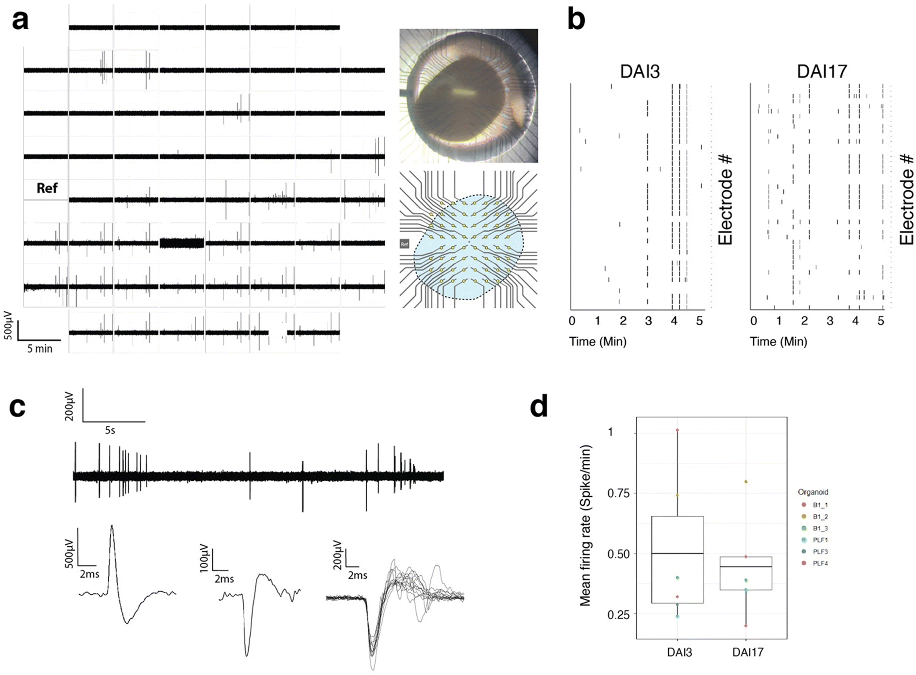 | ||
| Fig. 5 Cantilever microelectrodes reveal spontaneous intra-organoid electrical activity. (a) 5 min of electrical recording of the whole arrays of csMEA and representative photo and schematic of the csMEA array superposed to the position of the organoid showing the location of recording sites. (b) Measurement of detected spontaneous activity spikes of a single organoid impaled on csMEA at 3 and 17 days after impalement (DAI). (c) Traces and cut-outs of signal recorded with one electrode at 24 h and 4 days after impalement of the organoid. 30 s long acquisition and superposition of several detected spikes and examples of generic positive and negative typical signals. The recorded signal becomes stronger with time and goes up to several hundreds of μV. (d) Mean firing rate of cerebral organoids impaled on csMEA 3 and 17 DAI. | ||
Only a fraction (around 50–60%) of the electrodes where organoids were impaled showed electrical activity of high amplitude (>200 μV), with typical action potential shapes isolated from those, one reason being that the organoids do not fill the entire surface of the MEA, leaving some electrodes out. The rest are probably electrodes inserted in areas of the tissue where there are no active cells. Fig. 5 shows examples of traces recorded over 30 s and showing typical spontaneous activity. Fig. 5 also shows the superposition (cut out) of several spikes showing the typical shape of an extracellular recording of an action potential with depolarization and hyperpolarization and duration in the order of milliseconds. It also shows a typical recording of positive and negative signals with the same range of amplitude and dynamics.
The amplitude of the signals measured is higher than that usually measured with dissociated cells. This can be explained by the fact that the electrodes are placed close to the active cells, showing less leakage current, and by the strong compaction of the cells in the vicinity of the electrodes such as can be seen in Fig. 4(e), resulting from a reorganization of the cells over time after the insertion of the electrodes. The compaction of the cells around the electrodes could create a spatial limitation to the diffusion of ions expelled from ion channels in the intercellular space, which would have the effect of increasing the electric potential locally. This effect is also observed in potential measurement experiments around axons transiting in microtunnels, where the spatial confinement results in an increase in measured extracellular potentials,54,55 We also can notice some synchronous events that arise on several electrodes as noted on the raster plot of Fig. 5(b).
These results demonstrate that the use of microelectrodes positioned in a cantilever inserted inside a cerebral organoid is capable of measuring local potentials due to the electrical activity of electrically active cells with amplitudes of several hundred μV and typical shapes of extracellular recording.
Materials and methods
Microfabrication process
The manufacturing process for planar MEAs includes two lithography masks, one for the metal tracks, the other for the openings in the passivation layer. Here, we have added two additional levels of masking (4 levels in total), one to define the aluminum sacrificial layer shape and another to define the shape of the tip. The mask layout can be seen in Fig. 1(d). The microfabrication process is detailed in the process chart in Table ESI1.† It starts with a 4.9 cm × 4.9 cm, 500 μm thick glass blade (Paul Marienfeld GmbH) that is cleaned using the piranha process (sulfuric acid and peroxide) and dried with a nitrogen gun. Next, a 300 μm thick layer of aluminum is deposited by evaporation on the whole plate. The first lithography (mask #1) is made on the aluminum layer to define the sacrificial layer patterns, 2.5 inch masks are used on a Karl Suss MJB4 photomasker. A positive photoresist (PR) AZ 1518 (Microchemicals GmbH, Germany) is used to protect the metal during the aluminum wet etching step that is made using a mixture of H3PO4, HNO3, CH3COOH, and H2O (80/5/5/10%) at 40 °C. Etching control is made by optical inspection of the blade transparency.Next, the sandwich of compressive/metal/tensile materials is made. The deposition of silicon dioxide is made first by plasma enhanced chemical vapour deposition (PECVD) (Corial D250, Corial, France) at 280 °C using a mixture of SiH4, N2, O2 and Ar gases after a short process of surface cleaning. The silicon dioxide layer with compressive stress is deposited over 300 s for a thickness of about 800 nm.
After the SiO2 deposition, the metal that defines the electrode sites, routing and connection pads is deposited and patterned. For this we used the lift-off technique. Mask #2 is used to transfer the pattern using a negative lift-off photoresist (Microchemicals AZ nLOF 2020) that is slightly overdeveloped to create an undercut. Then, the metal thin layer (Ti 10 nm adhesion layer and Au 150 nm) is deposited by electron gun evaporation (Univex 450, Leybold). Gold is here preferred over platinum, which we usually use, because of its malleability that prevents the appearance of cracks in the metal, especially in the curvy beam location. After metal deposition on the whole plate, the photoresist is stripped using Remover PG at 80 °C and thoroughly cleaned to eliminate metal particles, followed by an additional piranha etch to remove resist residues. The second layer of stressed material, the tensile silicon nitride, is then deposited, also by PECVD at 280 °C over 300 s for a thickness of 800 nm. This layer also acts as an electrical insulation layer for the routing metal lines.
Finally, the last masks #3 and #4 are used to produce the openings that define the electrodes active sites and pads as well as the cantilevers. These steps are made by protecting the patterns with negative photoresist (AZ 2020, Microchemicals GmBH) and etching through the top silicon nitride down to the metal for the electrode and pads openings and through the stack of silicon nitride and silicon dioxide for the cantilever openings. Both of these steps are made using inductive plasma reactive ion etching (ICP-RIE) (Corial 200 L, Corial, France) with a mixture of CHF3, Ar and O2 gases. Etch control and end detection is made using a laser interference system. Note that these steps can be made in any order since these masks are non-overlapping. After these two plasma etch steps, the photoresist is stripped with an oxygen plasma step and the glass blades are additionally cleaned using a piranha wet etch. MEAs are fabricated by batch of 12 samples for some operations such as material deposition and processed one by one for photolithography. The result at this stage, i.e. before release, can be observed in Fig. 2(c). We usually obtain fabrication yields of around 80%.
Beam release and drying
The release of cantilevers is made by wet etching of the sacrificial layer, a 300 nm thick aluminum layer. The etching is made by using the same aluminum etch solution as described in the previous section. The etching of the sacrificial layer progresses from the edges of the beams and must therefore etch over about ten microns between the glass surface and the stack of layers that make up the beam; the etching time is of the order of a few tens of minutes and an optical control of the etching progress can be done optically by observing the etching front through the rear face of the substrate which is transparent. Beams can withstand large mechanical loads and displacements as long as they are applied along the beam axis and show large displacement amplitudes, but they are sensitive to loads when these are made off the beam axis. The drying stage at the end of the sacrificial layer etching is a delicate step since the capillary forces induced by the movement of the liquid and the meniscus can break the beams. To avoid this, we use a liquid with low surface tension, typically isopropanol, before the final nitrogen drying step. By using low nitrogen pressure and taking precautions for this drying phase we can easily obtain MEAs where all beams are intact. Also, we experienced no sticking of the released beams on the substrate.Culture rings
Cerebral organoids are compact millimeter-scale tissues and they need to be maintained at a location on top of the arrays of protruding beams. For this we use a piece of PDMS in the shape of a ring that is made by punching a 3 mm thick layer of PDMS using an 8 mm and 3 mm diameter punch (KAI Medical, Japan). This ring is then aligned under binoculars and plasma bonded around the beam region. This allows the cerebral organoid to be easily inserted and aligned on top of the active region. An outer ring is also used and bonded to the MEA in order to maintain the medium liquid. Both of these rings can be observed in Fig. 2(c).Stress measurement
Stress measurement is made by profilometry using a Veeco Dektak mechanical stylus profilometer with the bending plate method.56 SiO2 and Si3N4 layers are deposited using the exact same process as that used to produce the MEAs on two pieces of 2 inch silicon wafers. A profile of these wafers has been previously made with the stylus profilometer. The change in the radius of curvature between the wafer with and without the thin film layer allows the computation of the film stress. Surface profiles of these wafers can be observed in Fig. ESI1.†Organoid culture
Cortical organoids were derived from hESC H9 cells (female, WA09, WiCell) as previously described.53 The hESCs were cultured at 37 °C and 5% CO2 on Matrigel in mTeSR plus medium (Stemcell Technologies) supplemented with 1× penicillin–streptomycin (Thermo Fisher Scientific). For organoid production, cells were cultured on mitomycin-C-treated MEF feeder cell layers in DMEM/F12, L-glutamine, 20% KnockOut serum replacement, 1× NEAA, 100 μM β-mercaptoethanol and 1× penicillin–streptomycin, all purchased from Thermo Fisher Scientific. The medium was changed every day and supplemented with 8 ng mL−1 β-FGF (Sigma-Aldrich). After cell scooping using a cell lifter, embryonic bodies were transferred to a 60 mm ultra-low attachment dish (Corning) and cultured in differentiation medium: hESC medium supplemented with 1× sodium pyruvate (Thermo Fisher Scientific) and incubated at 37 °C and 5% CO2 on a rocker. After 24 h, half of the medium was changed with differentiation supplements: 3 μM IWR-1-Endo, 1 μM dorsomorphin, 10 μM SB-431542, and 1 μM cyclopamine, all reagents being purchased from Sigma-Aldrich. The medium was next fully changed every other day. The hESC differentiation medium was replaced at day 18 with Neurobasal medium (Thermo Fisher Scientific) complemented with 1× N2 supplement, 2 mM L-glutamine, 1× penicillin–streptomycin, and 1 μM cyclopamine. At day 24, cyclopamine was removed. Mature cortical organoids were gently transferred on top of the cantilever MEA. Slight pressure was exerted on top of the spheroids and gravity allowed the impalement on the electrodes. The medium was changed twice a week.Confocal microscopy
Cerebral organoids were fixed with 4% paraformaldehyde (PFA), permeabilized with 1% Triton X-100 and 0.5% BSA in PBS overnight and stained with anti-Pax6 (BioLegend), anti-GFAP (Novus Biologicals), anti-MAP2 (GeneTex), and anti-Bassoon (Abcam) antibodies for 12 h and then with fluorophore-coupled secondary antibodies and DAPI overnight. They were clarified overnight with RapiClear 1.52 reagent (Sunjin Lab) prior to image acquisition. Images were acquired using a spinning-disk confocal microscope (Dragonfly, Oxford Instruments) equipped with an ultrasensitive 1024 × 1024 EMCCD camera (iXon Life 888, Andor) and four laser lines (405, 488, 561, and 637 nm). A 20× air objective with a numerical aperture (NA) of 0.8 was used for whole-organoid imaging and a 100× oil-immersion objective with a NA of 1.45 (Nikon) was used for synapse imaging. For the 3D reconstruction, a stack of z steps with 1 μm interval was used for 20× images, and 0.3 μm for the 100× images. Images were processed by using Imaris ×64 (Bitplane) version 9.2 and 9.7. For the light sheet imaging, after the staining, the organoids were detached for the csMEA by cutting the cantilevers at the base. The imaging was done with the Miltenyi Light Sheet Ultramicroscope Blaze equipped with a 2560 × 2160 sCMOS camera and three laser lines (488, 561 and 637 nm). A 2× objective with a NA of 0.5 was used (MVPLAPO Olympus).Electrophysiology
The csMEA has been designed for use with the MEA2100-Mini-60-System (Multichannel Systems Gmbh, MCS). The MEA has been designed to fit this particular machine that comprises 60 channels. For extracellular electrophysiology experiments, MEAs with cerebral organoids impaled for 3 or 17 days were placed on the head stage and incubated at 37 °C and 5% CO2 with an aluminum foil wrap for electrical insulation. The medium was replaced >2 h prior to recording. Spontaneous electrical activity was recorded at a sampling rate of 20 kHz, amplified with the MEA2100-Mini-60-Sytem amplifier, and raw electrical data were recorded using the MCS experimenter software. For analysis, raw data were filtered with a 200–1000 Hz bandpass Butterworth filter using the MCS Analyzer software. Spikes were detected when the recorded voltage crossed a bidirectional threshold of 5 SDs, calculated over a 5 ms moving window. Mean firing rate (spikes per minute) was calculated for each recording and normalized to the number of active electrodes. Custom R scripts for threshold calculation and spike detection are available upon request.Conclusions
This paper has shown the development of a technique to produce curvy and spiky cantilever microelectrode arrays that are used to monitor the extracellular electrical activity inside cerebral organoids. Our specifications were to produce an array of cantilevers supporting microelectrodes that are much longer than usual (several hundredths of a micron) using conventional microfabrication techniques and without having to use complex deep etching steps, and moreover on a glass substrate. The solution we have proposed meets these conditions and we have demonstrated its ability to measure local potentials inside cerebral organoids. This work has demonstrated the ability of cantilever MEAs to measure action potentials with relatively strong signals while retaining the benefit of a transparent substrate that also allows fluorescence analyses such as calcium imaging, for example.With the increase in studies of brain organoids, which are a much more relevant model than dissociated cell cultures, this device provides an effective solution for measuring the internal extracellular electrical activity of these 3D cell clusters. This work has been made with cerebral organoids, but other electrically active organoids can be involved such as heart-forming organoids or muscle tissues. In the future, these devices could be used to monitor the electrical activity of organoids following, for example, virus infection with neurological effects in a biologically relevant model or to screen neuroactive drugs.
The continuation of this work will include the design and manufacture of devices comprising several electrodes per cantilever to adapt to the problem of the location of active cells deep within the organoid. The width of the beams will allow the integration of several electrodes and routing wires along them, allowing measurement of LFPs at different depths regarding the surface of the tissue. We will also be investigating the use of coatings on cantilevers to make them more resistant to mechanical deformations and to study their long-term biocompatibility.
Author contributions
BC and OP imagined the concept, designed the device, developed the microfabrication process and participated in the electrophysiology experiments. AS participated in the clean room microfabrication of the devices. EP and RG participated in the concept and carried out the organoid cultures, produced the confocal microscopy images and performed the electrophysiology experiments. CB participated in electrophysiology recordings and analysis. BC and RG wrote the manuscript.Conflicts of interest
The authors declare no competing financial interests.Acknowledgements
A part of this work was supported by the Isite MUSE of the University of Montpellier (BC), the ANR Agence Nationale de la Recherche (ANR-21-CE33-0007-03 to BC and RG), Sidaction (#21-1-AEQ-12958 to RG), a CBS2 doctoral school fellowship (EP), and the “ANRS-MIE/FRM” program (#MIE202207016212 to EP and RG). Authors thanks the MRI microscopy facilities and CTM university cleanroom in Montpellier for technical support.References
- J. Kim, B.-K. Koo and J. A. Knoblich, Nat. Rev. Mol. Cell Biol., 2020, 21, 571–584 CrossRef CAS PubMed.
- M. A. Lancaster, M. Renner, C.-A. Martin, D. Wenzel, L. S. Bicknell, M. E. Hurles, T. Homfray, J. M. Penninger, A. P. Jackson and J. A. Knoblich, Nature, 2013, 501, 373–379 CrossRef CAS PubMed.
- X. Qian, H. Song and G. Ming, Development, 2019, 146, dev166074 CrossRef CAS PubMed.
- N. V. Ayala-Nunez and R. Gaudin, PLoS Pathog., 2020, 16, e1008434 CrossRef CAS PubMed.
- I. Chiaradia and M. A. Lancaster, Nat. Neurosci., 2020, 23, 1496–1508 CrossRef CAS PubMed.
- S. L. Giandomenico, S. B. Mierau, G. M. Gibbons, L. M. D. Wenger, L. Masullo, T. Sit, M. Sutcliffe, J. Boulanger, M. Tripodi, E. Derivery, O. Paulsen, A. Lakatos and M. A. Lancaster, Nat. Neurosci., 2019, 22, 669–679 CrossRef CAS PubMed.
- A. M. Yakoub, Neural Regener. Res., 2019, 14, 757–761 CrossRef CAS PubMed.
- S. R. Fair, D. Julian, A. M. Hartlaub, S. T. Pusuluri, G. Malik, T. L. Summerfied, G. Zhao, A. B. Hester, W. E. Ackerman, E. W. Hollingsworth, M. Ali, C. A. McElroy, I. A. Buhimschi, J. Imitola, N. L. Maitre, T. A. Bedrosian and M. E. Hester, Stem Cell Rep., 2020, 15, 855–868 CrossRef CAS PubMed.
- S. Ghatak, N. Dolatabadi, D. Trudler, X. Zhang, Y. Wu, M. Mohata, R. Ambasudhan, M. Talantova and S. A. Lipton, eLife, 2019, 8, e50333 CrossRef PubMed.
- A. Kathuria, K. Lopez-Lengowski, S. S. Jagtap, D. McPhie, R. H. Perlis, B. M. Cohen and R. Karmacharya, JAMA Psychiatry, 2020, 77, 745–754 CrossRef PubMed.
- C. A. Trujillo, R. Gao, P. D. Negraes, J. Gu, J. Buchanan, S. Preissl, A. Wang, W. Wu, G. G. Haddad, I. A. Chaim, A. Domissy, M. Vandenberghe, A. Devor, G. W. Yeo, B. Voytek and A. R. Muotri, Cell Stem Cell, 2019, 25, 558–569.e7 CrossRef CAS PubMed.
- O. L. Eichmüller and J. A. Knoblich, Nat. Rev. Neurol., 2022, 18, 661–680 CrossRef PubMed.
- H. Wang and R. Balice-Gordon, Front. Synaptic Neurosci., 2022, 14, 846099 CrossRef PubMed.
- R. M. Marton and S. P. Paşca, Trends Cell Biol., 2020, 30, 133–143 CrossRef CAS PubMed.
- J. Antonucci and L. Gehrke, ACS Infect. Dis., 2019, 5, 1976–1979 CrossRef CAS PubMed.
- A. Ramani, A.-I. Pranty and J. Gopalakrishnan, Stem Cell Rep., 2021, 16, 373–384 CrossRef CAS PubMed.
- Brain organoids: advances, applications and challenges|Development|The Company of Biologists, https://journals.biologists.com/dev/article/146/8/dev166074/19861/Brain-organoids-advances-applications-and, (accessed October 27, 2021) Search PubMed.
- C. Forro, D. Caron, G. N. Angotzi, V. Gallo, L. Berdondini, F. Santoro, G. Palazzolo and G. Panuccio, Micromachines, 2021, 12, 124 CrossRef PubMed.
- R. A. Samarasinghe, O. A. Miranda, J. E. Buth, S. Mitchell, I. Ferando, M. Watanabe, T. F. Allison, A. Kurdian, N. N. Fotion, M. J. Gandal, P. Golshani, K. Plath, W. E. Lowry, J. M. Parent, I. Mody and B. G. Novitch, Nat. Neurosci., 2021, 1–13 Search PubMed.
- H. Sakaguchi, Y. Ozaki, T. Ashida, T. Matsubara, N. Oishi, S. Kihara and J. Takahashi, Stem Cell Rep., 2019, 13, 458–473 CrossRef CAS PubMed.
- Y. Nam and B. C. Wheeler, Crit. Rev. Biomed. Eng., 2011, 39, 45–61 CrossRef PubMed.
- P. Duc, M. Vignes, G. Hugon, A. Sebban, G. Carnac, E. Malyshev, B. Charlot and F. Rage, Lab Chip, 2021, 21, 4223–4236 RSC.
- E. Moutaux, B. Charlot, A. Genoux, F. Saudou and M. Cazorla, Lab Chip, 2018, 18, 3425–3435 RSC.
- D. Kim, H. Kang and Y. Nam, Lab Chip, 2020, 20, 3410–3422 RSC.
- O. Herreras, Front. Neural Circuits, 2016, 10, 101 Search PubMed.
- K. Tasnim and J. Liu, J. Mol. Biol., 2022, 434, 167165 CrossRef CAS PubMed.
- A. P. Passaro and S. L. Stice, Front. Neurosci., 2021, 14, 622137 CrossRef PubMed.
- T. Sharf, T. van der Molen, S. M. K. Glasauer, E. Guzman, A. P. Buccino, G. Luna, Z. Cheng, M. Audouard, K. G. Ranasinghe, K. Kudo, S. S. Nagarajan, K. R. Tovar, L. R. Petzold, A. Hierlemann, P. K. Hansma and K. S. Kosik, Nat. Commun., 2022, 13, 4403 CrossRef CAS PubMed.
- M. O. Heuschkel, M. Fejtl, M. Raggenbass, D. Bertrand and P. Renaud, J. Neurosci. Methods, 2002, 114, 135–148 CrossRef PubMed.
- A. Casanova, L. Bettamin, M.-C. Blatche, F. Mathieu, H. Martin, D. Gonzalez-Dunia, L. Nicu and G. Larrieu, J. Phys.: Condens. Matter, 2018, 30, 464001 CrossRef CAS PubMed.
- M. Dimaki, P. Vazquez, M. H. Olsen, L. Sasso, R. Rodriguez-Trujillo, I. Vedarethinam and W. E. Svendsen, Sensors, 2010, 10, 10339–10355 CrossRef CAS PubMed.
- A. P. Alivisatos, A. M. Andrews, E. S. Boyden, M. Chun, G. M. Church, K. Deisseroth, J. P. Donoghue, S. E. Fraser, J. Lippincott-Schwartz, L. L. Looger, S. Masmanidis, P. L. McEuen, A. V. Nurmikko, H. Park, D. S. Peterka, C. Reid, M. L. Roukes, A. Scherer, M. Schnitzer, T. J. Sejnowski, K. L. Shepard, D. Tsao, G. Turrigiano, P. S. Weiss, C. Xu, R. Yuste and X. Zhuang, ACS Nano, 2013, 7, 1850–1866 CrossRef CAS PubMed.
- J. T. Robinson, M. Jorgolli, A. K. Shalek, M.-H. Yoon, R. S. Gertner and H. Park, Nat. Nanotechnol., 2012, 7, 180–184 CrossRef CAS PubMed.
- J. C. Mateus, C. D. F. Lopes, M. Cerquido, L. Leitão, D. Leitão, S. Cardoso, J. Ventura and P. Aguiar, J. Neural Eng., 2019, 16, 036012 CrossRef PubMed.
- P. Le Floch, Q. Li, Z. Lin, S. Zhao, R. Liu, K. Tasnim, H. Jiang and J. Liu, Adv. Mater., 2022, 34, 2106829 CrossRef CAS PubMed.
- M. McDonald, D. Sebinger, L. Brauns, L. Gonzalez-Cano, Y. Menuchin-Lasowski, M. Mierzejewski, O.-E. Psathaki, A. Stumpf, J. Wickham, T. Rauen, H. Schöler and P. D. Jones, Biosens. Bioelectron., 2023, 228, 115223 CrossRef CAS PubMed.
- D. A. Soscia, D. Lam, A. C. Tooker, H. A. Enright, M. Triplett, P. Karande, S. K. G. Peters, A. Paula Sales, E. K. Wheeler and N. O. Fischer, Lab Chip, 2020, 20, 901–911 RSC.
- A. Kalmykov, J. W. Reddy, E. Bedoyan, Y. Wang, R. Garg, S. K. Rastogi, D. Cohen-Karni, M. Chamanzar and T. Cohen-Karni, J. Neural Eng., 2021, 18, 055005 CrossRef PubMed.
- A. Kalmykov, C. Huang, J. Bliley, D. Shiwarski, J. Tashman, A. Abdullah, S. K. Rastogi, S. Shukla, E. Mataev, A. W. Feinberg, K. J. Hsia and T. Cohen-Karni, Sci. Adv., 2021, 7(12), eabf9153 CrossRef PubMed.
- K. Tasnim and J. Liu, J. Mol. Biol., 2022, 434, 167165 CrossRef CAS PubMed.
- H. Shin, S. Jeong, J.-H. Lee, W. Sun, N. Choi and I.-J. Cho, Nat. Commun., 2021, 12, 492 CrossRef CAS PubMed.
- J. C. Williams, R. L. Rennaker and D. R. Kipke, Brain Res. Protoc., 1999, 4, 303–313 CrossRef CAS PubMed.
- M. A. L. Nicolelis, D. Dimitrov, J. M. Carmena, R. Crist, G. Lehew, J. D. Kralik and S. P. Wise, Proc. Natl. Acad. Sci. U. S. A., 2003, 100, 11041–11046 CrossRef CAS PubMed.
- J. J. Jun, N. A. Steinmetz, J. H. Siegle, D. J. Denman, M. Bauza, B. Barbarits, A. K. Lee, C. A. Anastassiou, A. Andrei, Ç. Aydın, M. Barbic, T. J. Blanche, V. Bonin, J. Couto, B. Dutta, S. L. Gratiy, D. A. Gutnisky, M. Häusser, B. Karsh, P. Ledochowitsch, C. M. Lopez, C. Mitelut, S. Musa, M. Okun, M. Pachitariu, J. Putzeys, P. D. Rich, C. Rossant, W. Sun, K. Svoboda, M. Carandini, K. D. Harris, C. Koch, J. O'Keefe and T. D. Harris, Nature, 2017, 551, 232–236 CrossRef CAS PubMed.
- M. Malerba, H. Amin, G. N. Angotzi, A. Maccione and L. Berdondini, in Cell-Based Microarrays: Methods and Protocols, ed. P. Ertl and M. Rothbauer, Springer, New York, NY, 2018, pp. 147–157 Search PubMed.
- L. Muzzi, M. Falappa, A. Maccione, D. di Lisa, M. Frega and S. Martinoia, in 2021 10th International IEEE/EMBS Conference on Neural Engineering (NER), 2021, pp. 123–127 Search PubMed.
- M. E. Obien, K. Deligkaris, T. Bullmann, D. J. Bakkum and U. Frey, Front. Neurosci., 2015, 8, 423 Search PubMed.
- V. Emmenegger, M. E. J. Obien, F. Franke and A. Hierlemann, Front. Cell. Neurosci., 2019, 13, 159 CrossRef CAS PubMed.
- J.-H. Kim, G. Kang, Y. Nam and Y.-K. Choi, Nanotechnology, 2010, 21, 085303 CrossRef PubMed.
- K. Janzakova, M. Ghazal, A. Kumar, Y. Coffinier, S. Pecqueur and F. Alibart, Adv. Sci., 2021, 8, 2102973 CrossRef CAS PubMed.
- A. Virlogeux, E. Moutaux, W. Christaller, A. Genoux, J. Bruyère, E. Fino, B. Charlot, M. Cazorla and F. Saudou, Cell Rep., 2018, 22, 110–122 CrossRef CAS PubMed.
- S. Timoshenko, J. Opt. Soc. Am., 1925, 11, 233–255 CrossRef CAS.
- N. V. Ayala-Nunez, G. Follain, F. Delalande, A. Hirschler, E. Partiot, G. L. Hale, B. C. Bollweg, J. Roels, M. Chazal, F. Bakoa, M. Carocci, S. Bourdoulous, O. Faklaris, S. R. Zaki, A. Eckly, B. Uring-Lambert, F. Doussau, S. Cianferani, C. Carapito, F. M. J. Jacobs, N. Jouvenet, J. G. Goetz and R. Gaudin, Nat. Commun., 2019, 10, 4430 CrossRef PubMed.
- L. Pan, S. Alagapan, E. Franca, T. DeMarse, G. J. Brewer and B. C. Wheeler, IEEE Trans. Neural Syst. Rehabilitation Eng, 2014, 22, 453–459 Search PubMed.
- M. K. Lewandowska, D. J. Bakkum, S. B. Rompani and A. Hierlemann, PLoS One, 2015, 10, e0118514 CrossRef PubMed.
- R. J. Jaccodine and W. A. Schlegel, J. Appl. Phys., 1966, 37, 2429–2434 CrossRef CAS.
Footnotes |
| † Electronic supplementary information (ESI) available. See DOI: https://doi.org/10.1039/d3lc00294b |
| ‡ Co-first author. |
| § Co-last author. |
| This journal is © The Royal Society of Chemistry 2023 |