 Open Access Article
 This Open Access Article is licensed under a Creative Commons Attribution-Non Commercial 3.0 Unported Licence
Iontronic microscopy of a tungsten microelectrode: “seeing” ionic currents under an optical microscope†
Zhu
Zhang
 * and
Sanli
Faez
* and
Sanli
Faez
Nanophotonics, Debye Institute for Nanomaterials Science, Utrecht University, 3584CC Utrecht, The Netherlands. E-mail: z.zhang@uu.nl
First published on 6th April 2023
Abstract
Optical methods for monitoring electrochemical reactions at an interface are advantageous because of their table-top setup and ease of integration into reactors. Here we apply EDL-modulation microscopy to one of the main components of amperometric measurement devices: a microelectrode. We present experimental measurements of the EDL-modulation contrast from the tip of a tungsten microelectrode at various electrochemical potentials inside a ferrocene-dimethanol Fe(MeOH)2 solution. Using the combination of the dark-field scattering microscope and the lock-in detection technique, we measure the phase and amplitude of local ion-concentration oscillations in response to an AC potential as the electrode potential is scanned through the redox-activity window of the dissolved species. We present the amplitude and phase map of this response, as such this method can be used to study the spatial and temporal variations of the ion-flux due to an electrochemical reaction close to metallic and semiconducting objects of general geometry. We discuss the advantages and possible extensions of using this microscopy method for wide-field imaging of ionic currents.
1 Introduction
Electroreflectance, electric field modulation of optical reflectivity, is a well-established method for investigating the nanoscale surface layer at metal–electrolyte interfaces.1–6 This signal is both sensitive to the carrier concentration on the metallic side as well as the ion concentration in the electric double layer.7 It has been used in the past to investigate band structures of the conducting side, as well as the electrochemical processes at the interface. The early measurements of electroreflectance used far-field reflection from flat surfaces, similar to ellipsometry, to measure the minuscule changes of the reflectance due to the restructuring of the interfacial layer. In those geometries, the spatial resolution is given by the illumination beam size, which is not suitable for investigating sub-ten-micrometer spatial variations. Obtaining real-space surface images of electrochemical activity using optical reflection was made possible using interferometric methods8–10 or using surface plasmon imaging.11 Plasmonic-enhanced measurements, however, are mainly suitable for the surface of noble metals such as gold.Adapting and applying this powerful optical method to nanoscale non-plasmonic structures and interfaces has proven difficult because of the optical diffraction limit and steep decrease of the scattering signal from sub-diffraction nano-objects. Metallic nanoparticles that exhibit a plasmonic resonance12–18 and some 2D materials,19 have been notable exceptions. In this domain, the resonance enhancement of scattering allows, for example, the investigation of nanorods as small as 20 nanometers.15,16 The signal in those investigations, however, is dominated by the electronic density inside the particle, and not all metallic particles exhibit a clear plasmon resonance in the visible range. Furthermore, as the carrier dynamics on the metallic side of the interface dominate the signal, investigation of the ionic currents in the electrolyte is only be possible via indirect interpretations and modeling.
Recently, our group demonstrated a new optical contrast mechanism for non-plasmonic or dielectric particles based on a periodic modulation of the substrate potential,20 relative to an electrode in the bulk of the liquid. In this method, modulating the EDL close to the surface results in scattering signals that are sensitive to both the local topography and electrochemical properties of the investigated region. Interestingly, the relative contrast in this interferometrically enhanced method increases with decreasing size of the particle. We have dubbed our method EDL-modulation microscopy, which can be categorized as a subclass of iontronic microscopy methods. Recent advances in interferometric scattering microscopy and computational modeling of the electric double layer formation indicate that sensing a single surface charge alteration is within technical reach.21 Merryweather et al. resolved nanoscopic lithium-ion dynamics in a solid-state battery based on interferometric scattering microscopy.22,23 Valavanis et al. demonstrated the combination of scanning electrochemical cell microscopy (SECCM) and interference reflection microscopy (IRM) to monitor electrochemically-driven phase formation phenomena with high spatial and temporal resolution.24 Utterback et al. spatiotemporally resolved an electrochemically-induced ion concentration gradient evolution in solution using IRM.25
In this contribution, we present experimental measurements of the EDL-modulation contrast from the tip of a tungsten microelectrode at various electrochemical potentials inside a ferrocene-dimethanol (Fe(MeOH)2) solution. This is possible as a unique feature of EDL-modulation microscopy because the observed signal does not depend on local resonances. Our main goal is to investigate the spatial extent of the electrochemical reaction zone close to the microelectrode tip, with optical imaging. Contrary to our previous measurements on transparent ITO substrates, measuring the microelectrode allows us to make a direct correlation between the electric current passing through the tip of the electrode and the observed optical modulation signal. While, in this paper, we use a confocal scanning method for building the image, this microscopy method is in principle compatible with wide-field imaging on a camera. Achieving a simultaneously high temporal and high spatial resolution is essential for filtering out the electrochemical noise caused by surface heterogeneity, which is a nuisance in conventional amperometry measurements. Furthermore, this dynamic and correlative measurement allows us to separate the contribution of surface ion absorption to the potentiodynamic scattering signal from that of the diffuse double layer, which in turn can provide new insights into the dynamics of complex surface electrochemical processes.
In the following, we first describe our measurement setup and experimental conditions. Next, we present the signal of the lock-in enhanced EDL-modulation optical imaging from the tip of the microelectrode and discuss its dependence on the concentration of reagents, the modulation frequency and the modulation amplitude. Finally, we present the confocal maps of the intensity and detected modulation phase around the tip. We will conclude by presenting our perspective on using the EDL-modulation microscopy method for electrochemical imaging.
2 Results
2.1 Measurement setup
The EDL-modulation microscopy setup is based on total-internal-reflection (TIR) illumination and scattering. The evanescent light field, incident on the interface, illuminates objects that are in the roughly 200 nm vicinity of the glass slide and inside the solution.Fig. 1(a) depicts the setup. A laser beam (ignis, 640 nm, Laser quantum) is focused off-axis in the back focal plane of an oil-immersion objective (Nikon, CFI Apochromat TIRF 60×, 1.4 NA), giving rise to TIR. The sensitive signal is derived from the scattering of the evanescent light field, which is imaged by a scientific complementary metal-oxide semiconductor (sCMOS) camera (ORCA-Flash 4.0 V3, Hamamatsu) and by a Photodetector (PD, PWPR-2K-SI, FEMOTO).
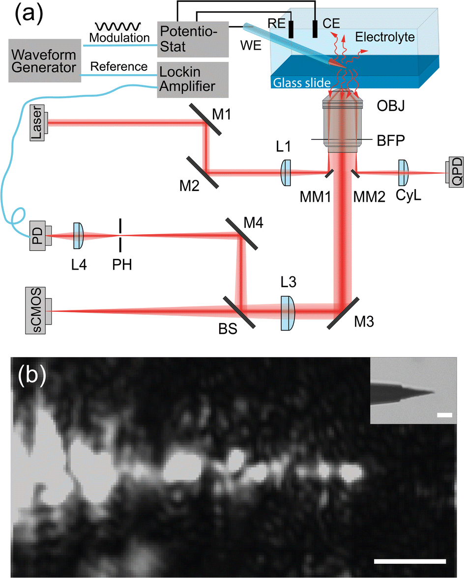 | ||
| Fig. 1 (a) Schematic of the setup. M1–M4: adjustable mirrors; L1 and L2: beam focus lens; L3 and L4: imaging lens; MM1, MM2: small prism mirrors; OBJ: microscope objective; BFP: back focal plane of the microscope objective; CyL: cylindrical lens; RE: reference electrode in the chemical cell; CE: the counter electrode in the chemical cell; BS: beam splitter; PH: pinhole; PD: photodiode; sCMOS: scientific complementary metal-oxide-semiconductor camera; QPD: quadrant photodiode. (b) Light-scattering image of the tungsten tip, inset: the bright-field image of the tungsten tip. Scale bar: 5 μm. | ||
This method is similar to total-internal-reflection-fluorescence (TIRF) microscopy, which excites the fluorescent objectives at the interface with an evanescent field and images the corresponding fluorescence emission light.26–28 Instead of imaging fluorescence emission light from objectives, the experimental instrument here detects the scattering light that reaches objectives. That means it allows us to image any dielectric object that is closer than roughly 200 nm to the interface. Meng et al. implemented this method to track single gold nanoparticles at oil–water interfaces29 and Namink et al. used this method to image electric double charging/discharging dynamics around small ITO nanoparticles during potential modulation.20 For this paper, we have improved the detection sensitivity of our setup by including a photodiode and a lock-in amplifier in the imaging path, which improves the detection sensitivity, modulation divided by net scattering, from 10−3 (ref. 20 and 29) to 10−5–10−6 using lock-in detection. This extra sensitivity comes at the cost of imaging speed as one needs to scan the sample to build an image.
We use a 3D piezo stage (P-611.3 Nanocube, Physik Instrumente) to hold the glass slide and the microelectrode, the piezo stage precisely scans the sample in the xy plane to get a 2D image. The microelectrode we used in the experiments is a tungsten microelectrode (Microelectrodes Ltd, Cambridge, UK). In the inset of Fig. 1(b), we show the bright field image of the microelectrode tip. The length of the exposed tip is about 15 μm with a tip diameter of 2 μm at the very end, with a diameter of 10 μm close to the glass insulation layer. The rest of the microelectrode is insulated by a thin glass layer with a thickness of 1 μm close to the tip and a thickness of 40 μm at the shank.
We use a high-precision waveform generator (33120 A, 15 MHz, HP) to generate a modulation signal and a reference. The modulated signal is sent to a potentiostat (E162 picostat, or EA362 Dual picostat, eDAQ), which accurately controls the cell potential during the experiments. The reference signal is sent to the lock-in amplifier. The corresponding potential and current signal from the electrochemical cell are recorded and amplified by a data recorder (e-corder 410, eDAQ). During the potential modulation, the variation in the scattering light intensity from the investigated objects is collected by the PD, which converts light to current and amplifies the current to voltage signal (with bandwidth 2 K and transimpedance gain of 109 Ω). The amplified light intensity is sent to a lock-in amplifier (SR830 DSP lock-in Amplifier, Stanford Research System). The lock-in amplifier calculates the amplitude of the light intensity variations caused by the potential modulation. We use a Data Acquisition card (DAQ, NIUSB-6212, National Instrument) to synchronize the waveform generator, lock-in amplifier, potentiostat and collect all the signals through a Python program.
It is possible to combine the lock-in method with wide-field imaging using an sCMOS camera and programming fast detection electronics.30 However, the discussion of such advanced imaging modalities is beyond the scope of this paper. To get a stable signal, the setup and illumination beam must be actively stabilized. These details are described elsewhere.31
2.2 The sample
We perform scanning EDL-modulation measurements on a tungsten microelectrode (Microelectrodes Ltd, Cambridge, UK) in Fe(MeOH)2, dissolved in 100 mM KCl solution as the support electrolyte.In the experiment, we add a potential modulation to the offset potential scanned with a triangular shape. In conventional amperometric measurements, this method is best known as AC-voltammetry (ACV). In ACV measurements, we refer to the offset as DC potential scan, and the potential modulation as AC potential, their corresponding currents are DC currents and AC currents.
As shown in Fig. 2(a), the pink line presents the potential applied to the tungsten electrode, which is the superposition of an AC sinusoidal modulation potential with amplitude of 50 mV, frequency of 75 Hz and a linear triangle offset potential altering from −0.25 V to 0.3 V. The currents from the redox reaction of Fe(MeOH)2 are shown by a grey line, we can see that the oscillation of the current is boosted in the Fe(MeOH)2 redox potential window (around the potential of 0.05 V). Because of the potential modulation to the tungsten electrode, the light scattering intensities oscillate with respect to the potential, and the oscillation amplitude of the optical signal is detected by the lock-in amplifier.
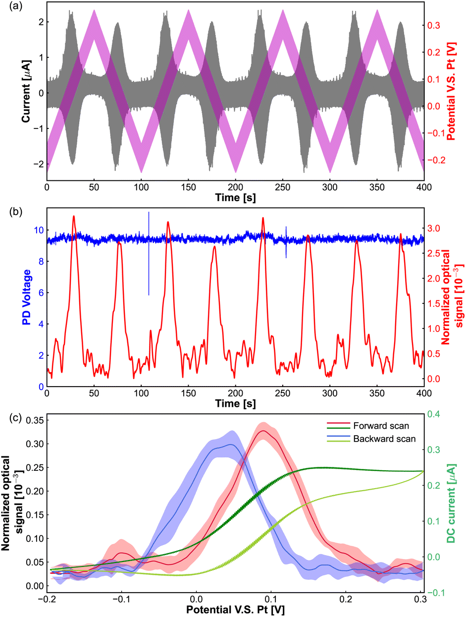 | ||
| Fig. 2 (a) Total AC current voltammogram (grey): the measured total electrical current through the microelectrode and the potential (pink) is scanned with a sine-modulated AC potential of 50 mV amplitude added to a gradually scanning DC offset. (b) Optical amplitude of lock-in signal (red) and the PD signal (blue). (c) Averaged optical amplitude of lock-in signal (blue and red) and the DC current component (green) extracted from total AC current voltammogram. DC potential scan from −200 mV to 300 mV with a scanning rate of 10 mV s−1, frequency of potential modulation is 75 Hz, the amplitude of potential modulation is 50 mV, and the concentration of Fe(MeOH)2 is 5 mM. | ||
The red curve in Fig. 2(b) shows the oscillation amplitude of the optical signal as a function of the DC scan potential. The blue curve in Fig. 2(b) represents the light scattering intensities collected by the PD during the ACV measurements. It is difficult to distinguish the changes or any trend by eye from the PD signal. However, with the lock-in amplifier, we can get the corresponding oscillation amplitude of the optical signal from the PD signal.
In the potential window of the electrochemical reactions, the oscillation amplitude of the optical signal goes up and returns back to the base value (around 0.05 × 10⁻³). Fig. 2(c) shows the optical signal as a function of applied DC potential, which is an average of 4 cycles from the red curve in Fig. 2(b) The dark green and light green lines are the (average) DC part extracted from the measured current passing through the microelectrode in Fig. 2(a).
Next, we use the piezo stage to scan the measurement spot. Fig. 3 (top panel) shows the 2D scanning image of the tungsten tip, which is reconstructed from the scattering light intensity while the DC potential was kept at 75 mV and −250 mV, in the potential modulation with a frequency of 95 Hz and modulation amplitude of 50 mV. The red dashed line shows the rough shape and direction of the tip. Note that because of the TIR configuration, only the parts of the tip that are in contact with the substrate can be visualized. The middle panel shows the reconstructed 2D image from the optical amplitude of lock-in signal. The bottom panel shows the reconstructed 2D image from the optical phase of lock-in signal. The optical lock-in signal is higher around the tungsten tip at the redox potential window of Fe(MeOH)2 (left middle panel), while the potential is out of the redox potential window, the optical lock-in signal is weaker (right middle panel).
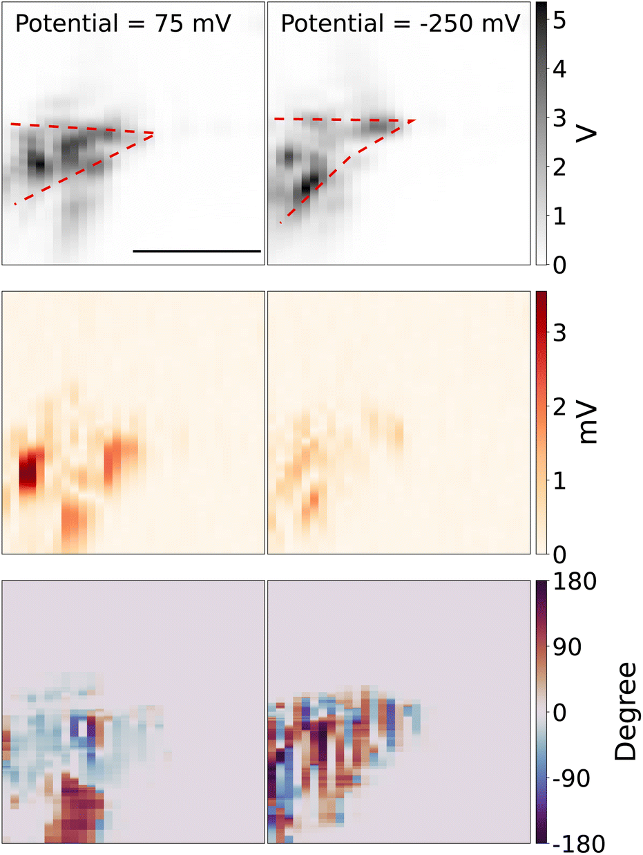 | ||
| Fig. 3 2D scan plot of the tip at potential 75 mV and −250 mV. Top panel: light intensity from the photodiode. Middle panel: optical signal from the lock-in amplifier. Bottom panel: phase plot. DC potential was kept at 75 mV (left) and −250 mV (right), in the potential modulation with a frequency of 95 Hz and modulation amplitude of 50 mV, the concentration of Fe(MeOH)2 is 15 mM. Scale bar: 5 μm. To avoid the random noise in the phase maps, the phase information is not displayed outside of the tip area, where the tip scattering light intensity is smaller than 10% of the maximum intensity. | ||
Note that the diffusion time of Fe(MeOH)20/+, K+ and Cl− around the tungsten microelectrode tip is given by τi = r2/Di, r is the mean diameter of the exposed tip of the tungsten microelectrode r = (10 + 2)/2 = 6 μm and Di denotes the diffusion coefficient of Fe(MeOH)20/+, K+ and Cl−. With the diffusion constant of DFc = 6.3 × 10⁻¹⁰ m2 s−1 and DK+ ≈ DCl− ≈ 2.0 × 10⁻⁹ m2 s−1,32,33 we can get the diffusion time τFc = 1/70 s and τK+ ≈ τCl− ≈ 1/200 s. In the 2D scanning experiments, the periodicity of the modulation (in a few hundred Hz) is shorter than the diffusion time τi, which indicates the modulated diffusion of Fe(MeOH)20/+ is indeed around the tip area. For the modulated diffusion of K+ and Cl−, they can diffuse slightly further away from the tip than Fe(MeOH)20/+.
We can see that the reconstructed 2D images are “blotchy”, the reason is that the surface of the tungsten microelectrode is heterogeneous which makes the contacts between the microelectrode tip and glass slides heterogeneous. Since the evanescent field strength at the surface is significant depends on the distance between the microelectrode and glass surface, the hetergenerous contacts makes the scattering light higher at the places where the tip surface is close to the glass surface and the scattering light weaker at the place where the tip surface is not well contacted with the glass surface. The tip shape changes due to the drift of the holder between these two measurements, which are taken about an hour apart. The bottom panel shows the phase of the lock-in response, which represents the delay between the local modulation of the scattering intensity and the applied potential to the tip.
Before discussing the two-dimensional scanning results, we discuss some control measurements obtained from the signal of the electrode tip.
In Fig. 4 we show the peak amplitude and phase of the modulation signal, observed in the middle of the redox-reactivity window, as a function of Fe(MeOH)2 concentration. The current response (containing AC component and DC components) as a function of Fe(MeOH)2 concentration is provided in ESI Fig. S2.† A close to a linear relationship is observed, testifying to the sensitivity of the modulation signal to the concentration of the electrochemically active species. Similarly, the measured signal scaled linearly with the modulation amplitude (Fig. S1 in ESI†). Both of these results are indications that the scattering modulation signal, for the conditions set in our experiments, is dominated by a first-order function of the analyte concentration in the solution adjacent to the electrode.
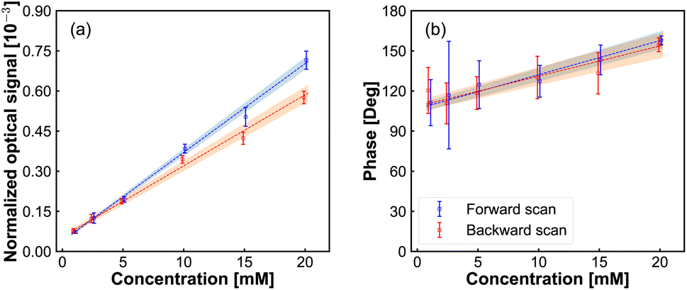 | ||
| Fig. 4 Normalized optical amplitude (a) and phase (b) signals from lock-in amplifier vs. Fe(MeOH)2 concentration. DC potential scan from −200 mV to 300 mV with a scanning rate of 40 mV s−1, frequency of potential modulation is 75 Hz, the amplitude of potential modulation is 50 mV. | ||
Next, we investigate the lock-in response dependence on the potential modulation frequency. These results are presented in Fig. 5. The lock-in signal decreases with increasing frequency, while the phase displays a semi-circle shape. Due to the limited bandwidth of our photodetector, we cannot be certain that the absolute phase lag at different frequencies is caused by the dynamics at the electrode tip and not by the response time of our photodetector when the frequency is higher than the bandwidth of our PD. To avoid that, we keep the modulation frequency below the bandwidth (2 kHz) of the PD. However, we still cannot exclude the effect of the RC circuit response of the chemical cell on the amplitude and phase. We then checked the electrical current response as a function of frequency modulation (Fig. S3 in ESI†). In Fig. S3† we show the current response as a function of modulation frequency. Fig. S3(a)† shows the amplitude of the AC current component, the slope of 1/2 of the amplitude versus modulation frequency in the double logarithmic plot, which is the Randles–Sevick electron transfer process involving freely diffusing redox species. Fig. S3(b)† shows the phase of the AC current component with respect to the phase of modulation potential, the dashed line is fitted to the data point to guide the eye. From the phase information of the AC current, we still cannot tell if the changes come from the modulation frequency difference or from the RC circuit. Fig. S3(c)† shows the DC current component, the DC current slowly increases with the increase of the modulation frequency.
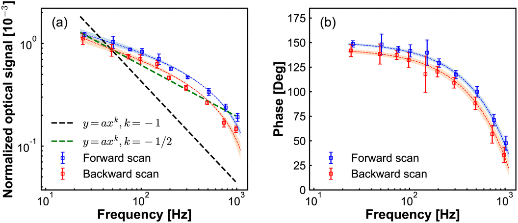 | ||
| Fig. 5 Normalized optical amplitude (a) and phase (b) signals from lock-in amplifier with different frequency of potential modulation. DC potential scan from −200 mV to 300 mV with a scanning rate6 of 50 mV s−1, the amplitude of potential modulation is 50 mV, and the concentration of Fe(MeOH)2 is 15 mM. | ||
In Fig. 5(a), the slope of −1/2 of modulation signal versus modulation frequency in the double logarithmic plot, resembles that for the Randles–Sevcik equation for cyclic voltammetry of electrochemically reversible electron transfer processes involving freely diffusing redox species.34 While the current increases proportional to the square root of the modulation frequency in conventional cyclic voltammetry (see Fig. S3(a) in ESI†), here the measured optical signal decreases. This difference can be understood by considering that the potentiodynamic signal in EDL-modulation microscopy originated from the ionic concentration variation at the electrode, as opposed to the ionic current variation in the conventional electrochemical measurement.
Following this analogy, if also theoretically verified, we can anticipate that our modulation frequency can also differentiate between the free diffusion effect on electrochemical processes and the influence of adsorbed species.
Next, we present and discuss the spatial variations of the modulation amplitude, and most significantly its lock-in phase. Fig. 6 displays the spatial map of the modulation signal around the tungsten tip as the sample stage is scanned over the objective. The left panel shows the 2D-scan images of the tungsten tip, which is reconstructed from the scattering light intensity while the DC potential was kept at a constant potential both in and out of the redox potential window of Fe(MeOH)2, in the potential modulation with the frequency of 95 Hz and modulation amplitude of 50 mV. The shape and direction of the tip are similar to the tip in Fig. 3. Since the tip is barely in contact with the slide, during measurements over hours, the tip gradually drifts on the slide surface, and hence changes the scattering pattern slightly. The sliding behavior caused the contact angle and contract position changes and can also result in discrepancies in the scattering light 2D images in different DC potentials.
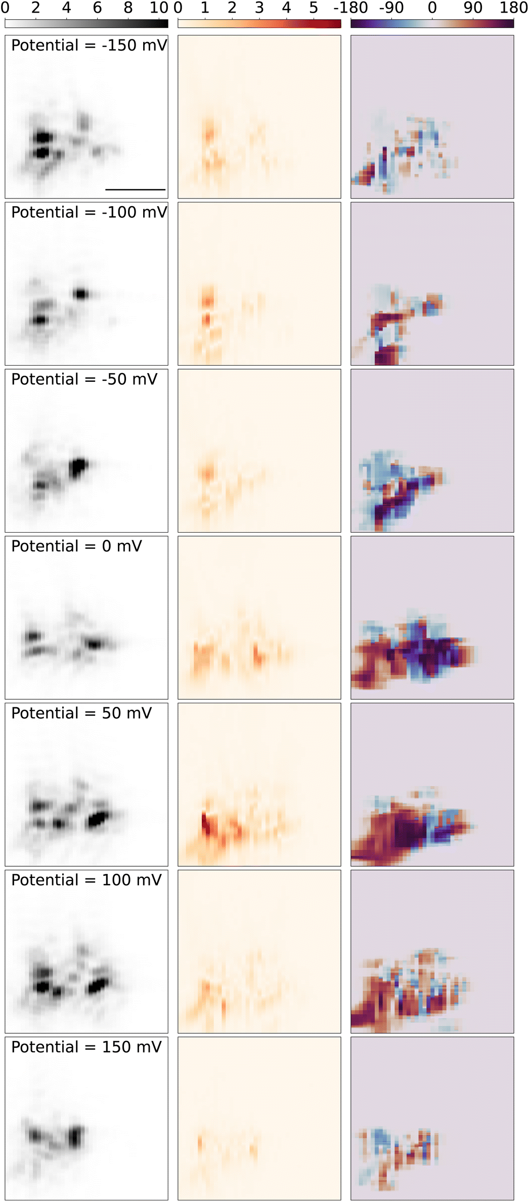 | ||
| Fig. 6 2D scan plot of the tip at different potentials. Left panel: scattering light intensity from PD, unit: V. Middle panel: optical signal from lock-in amplifier, unit: mV. Right panel: phase plot, unit: degrees. DC potential was kept at −150 mV (1st row), −100 mV (2nd row), −50 mV (3rd row) and 0 mV (4th row), 50 mV (5th row), 100 mV (6th row), 150 mV (7th row), in the potential modulation with the frequency of 95 Hz, and amplitude of 75 mV, the concentration of Fe(MeOH)2 was 15 mM. Scale bar: 5 μm. | ||
The middle panel in Fig. 6 shows the reconstructed 2D images from the optical PD signal, amplitude and phase from the lock-in response. When the DC potential is kept out of the redox potential window of Fe(MeOH)2 −150 mV (1st row), and hence there is no electrochemical reaction around the tip, the optical lock-in signal shows the light scattering variations only induced by the K+ and Cl− ions charging/discharging around the tungsten tip. While the DC potential is approaching from −150 mV to the redox potential of Fe(MeOH)2 at 50 mV, the oscillation amplitude of the optical signal increases. As the DC potential is closer to the redox potential, more Fe(MeOH)2 molecules are involved in the redox reactions. With more Fe(MeOH)2 molecule redox reactions around the tip, the variation of the optical signal is larger. When the DC potential is kept in the redox potential window of Fe(MeOH)2 50 mV (5th row), there are redox reactions of Fe(MeOH)2 and Fe(MeOH)+2, as well as the K+ and Cl− ions charging/discharging around the tip. The optical lock-in signal shows the light scattering variations both induced by the redox reaction of Fe(MeOH)2 and Fe(MeOH)2+, as well as K+ and Cl− ions charging/discharging around the tungsten tip.
The right panel in Fig. 6 shows the reconstructed 2D phase maps from the optical lock-in phase signal. As the tungsten tip is scanning out of the view of the PD detection, the low input signal (mostly from background scattering) results in a small lock-in component and the identified phase value show sporadic variations. To avoid the random noise in the phase maps, the phase information is not displayed outside of the tip area, where the tip scattering light intensity is smaller than 10% of the maximum intensity. As the frequency of the modulation is constant while scanning the measurement area over the tip, we can trust that the phase variation originates solely from the concentration dynamics of the redox-active species close to the electrode tip, and not the other electronic elements in the measurement circuit.
Fig. 7 shows the 2D scanning imaging around the tungsten with different modulation frequencies. The top panel shows the 2D scan images of the tungsten tip, which is reconstructed from the scattering light intensity while the DC potential was kept at close to the redox potential window of Fe(MeOH)2 50 mV, with the potential modulation amplitude of 75 mV. The shape and direction of the tip are similar to the tip shown in Fig. 3.
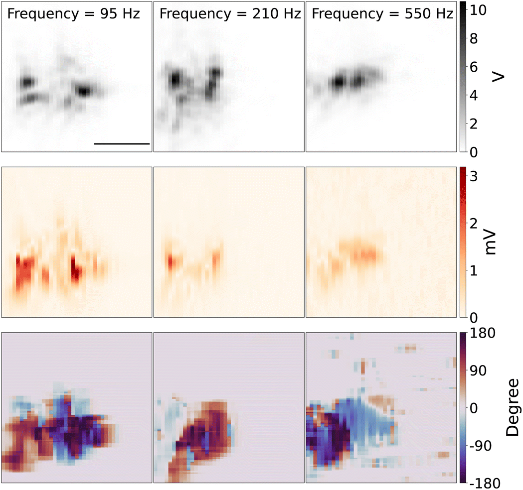 | ||
| Fig. 7 2D scan images of the tungsten tip at different modulation frequencies. Top panel: light intensity from the photodiode. Middle panel: optical signal from the lock-in amplifier. Bottom panel: phase plot. AC modulation frequency was 95 Hz (1st column), 210 Hz (2nd column), 550 Hz (3rd column), DC potential was kept at 0 mV, in the potential modulation with the amplitude of 75 mV, the concentration of Fe(MeOH)2 was 15 mM. Scale bar: 5 μm. | ||
The middle row panel in Fig. 7 shows the reconstructed 2D images from the optical PD signal, amplitude and phase of lock-in response. Since the DC potential was kept around the redox potential of Fe(MeOH)2, there are redox reactions of Fe(MeOH)2 and Fe(MeOH)2+, as well as the K+ and Cl− ions charging/discharging around the tungsten tip. The optical lock-in amplitude signal shows the light scattering variations, which is in this regime, linearly proportional to the ion concentration of the species with the highest optical polarisability. With lower modulation frequency, the optical lock-in signal is higher, and the signal area is larger. The redox species and K+ and Cl− can diffuse further away from the tungsten. With higher modulation frequency, the optical lock-in signal is weaker, and the 2D scanning signal area is smaller. The bottom row panel in Fig. 7 shows the reconstructed 2D images from the optical lock-in phase signal.
As the DC potential and the amplitude of the modulation is constant while scanning the measurement area over the tungsten tip, with the higher modulation frequency, the lock-in signal is smaller, which results in visible shrinking of the EDL-modulation image of the tip. One interpretation of this observation can be that the density variation of the species and K+ and Cl− can only diffuse to a limited distance away from the electrode surface. The refractive index variations around the tungsten tip caused by the concentration of molecules and ions is then smaller compared to low frequency modulation.
3 Discussion
By combining the dark-field scattering microscope and the lock-in detection technique, we introduce a label-free and operando method to measure the ion concentration variations during electrochemical reactions around a tungsten microelectrode with the equivalent of the AC-voltammetry technique. We have presented the alteration of this signal in the reversible electrochemical reaction window of Fe(MeOH)2. Since the dark-field scattering microscope is based on the principle of total-internal-reflection, the optical signal is only sensitive in the area where the tungsten tip contacts the glass slide, where it can scatter the evanescent field at the surface.We have measured the optical signal with different AC modulation amplitude, AC modulation frequency, DC potential and different concentrations of Fe(MeOH)2. We found that the dynamics of ion transport vary with both the AC modulation frequency and the concentration of Fe(MeOH)2. The dynamics of ion transport also highly varies based on the surface topography and the contact between the electrode glass cover and the glass slide.
In this paper, we have shown a proof of principle of obtaining dynamic images with EDL-modulation microscopy. We can foresee that the method is suited more to measuring structures fixed on the substrate, or by creating a pattern of nanoparticles as local transducers of the EDL-modulation signal. To quantitatively analyze the dynamics of ion transport, it is better to make a grid pattern of micro/nanoscopic objects on the surface, which can scatter light from the evanescent field close to the surface, such as nanoparticle array, nanodisk array35 and nanowire array.36,37 These well-defined structures also allow for stable measurements over a longer time-scale and can therefore be used for systematic measurements with a range of different experimental parameters.
Similar operando images of ion transport inside micro/nanoparticles, such as the diffusion of lithium-ions in single microparticles, is observed by monitoring the relative change of scattering light intensity of the microparticle during lithiation and delithiation processes,22,23 the lithium-ion diffusion kinetics of single LiCoO2 nanoparticles are imaged by surface plasmon resonance microscopy (SPRM),38,39 the electrochemical reaction kinetics of Prussian blue (PB) nanoparticles and K+ ion diffusion inside PB nanoparticles are captured by SPRM,40 total internal reflection microscopy41 and dark-field microscopy,42 and the monitoring and differentiating of the electrodeposition dynamics of metallic Ni and Ni(OH)2 nanoparticles on ITO slide are introduced by imaging their bright-field optical contrast.43 The ion transport during electrochemical reactions in such environments or inside a solution can be a complex process following coupled nonlinear differential equations of motion, for each charged species, coupled to the Laplace equation for the electric field distribution.8,25,44,45
At this point, the dynamics of our system seem to be too complex to model with a quasi-stationary or one-dimensional approximation46–48 and one has to solve the complete time-dependent equations to resolve the dynamics of ion transport temporally and spatially.25,49–53 However, the possibility of simultaneous measurements of the dynamic ion-density response around a micro- or nano-structure, as we have demonstrated in this paper, can be hugely beneficial for testing the validity of models proposed for the numerical simulation of such complex processes. Meanwhile, using semi-heuristic models and calibration relative to well-studied processes, one can also use this technique as a label-free tool for electrochemical measurements in ultra-small volumes and for ultra-low current levels.
Author contributions
Zhu Zhang: methodology, experimental measurements, investigation, visualization, writing original draft preparation. Sanli Faez: conceptualization, methodology, writing original draft preparation, writing, reviewing and editing, supervision.Conflicts of interest
There are no conflicts to declare.Acknowledgements
We thank Allard P. Mosk, Serge Lemay, Frédéric Kanoufi, Jean-François Lemineur, Louis Godeffroy and Haolan Tao for fruitful discussions. We thank Paul Jurrius, Dante Killian, Aron Opheij and Dave J. van den Heuvel for technical support. We thank Microelectrodes Ltd for providing the tungsten microelectrode. This research was supported by the Netherlands Organization for Scientific Research (NWO grant 680.91.16.03), China Scholarship Council (CSC 201806890015).Notes and references
- J. Feinleib, Phys. Rev. Lett., 1966, 16, 1200–1202 CrossRef CAS.
- A. Prostak and W. N. Hansen, Phys. Rev., 1967, 160, 600–601 CrossRef CAS.
- M. Stedman, Chem. Phys. Lett., 1968, 2, 457–460 CrossRef CAS.
- A. B. Buckman and N. M. Bashara, Phys. Rev., 1968, 174, 719–721 CrossRef CAS.
- B. J. Parsons, Phys. Rev., 1969, 182, 975 CrossRef CAS.
- A. Bewick and A. M. Tuxford, Symp. Faraday Soc., 1970, 4, 114–125 RSC.
- J. McIntyre, Surf. Sci., 1973, 37, 658–682 CrossRef CAS.
- Q. Li and H. S. White, Anal. Chem., 1995, 67, 561–569 CrossRef CAS.
- G. Flätgen, K. Krischer, B. Pettinger, K. Doblhofer, H. Junkes and G. Ertl, Science, 1995, 269, 668–671 CrossRef PubMed.
- O. Andersson, C. Ulrich, F. Björefors and B. Liedberg, Sens. Actuators, B, 2008, 134, 545–550 CrossRef CAS.
- X. Shan, U. Patel, S. Wang, R. Iglesias and N. Tao, Science, 2010, 327, 1363–1366 CrossRef CAS PubMed.
- S. R. Kirchner, K. W. Smith, B. S. Hoener, S. S. E. Collins, W. Wang, Y.-Y. Cai, C. Kinnear, H. Zhang, W.-S. Chang, P. Mulvaney, C. F. Landes and S. Link, J. Phys. Chem. C, 2018, 122, 6865–6875 CrossRef CAS.
- C. P. Byers, B. S. Hoener, W.-S. Chang, M. Yorulmaz, S. Link and C. F. Landes, J. Phys. Chem. B, 2014, 118, 14047–14055 CrossRef CAS PubMed.
- C. P. Byers, B. S. Hoener, W.-S. Chang, S. Link and C. F. Landes, Nano Lett., 2016, 16, 2314–2321 CrossRef CAS PubMed.
- B. S. Hoener, H. Zhang, T. S. Heiderscheit, S. R. Kirchner, A. S. De Silva Indrasekara, R. Baiyasi, Y. Cai, P. Nordlander, S. Link, C. F. Landes and W.-S. Chang, J. Phys. Chem. Lett., 2017, 8, 2681–2688 CrossRef CAS PubMed.
- B. S. Hoener, C. P. Byers, T. S. Heiderscheit, A. S. De Silva Indrasekara, A. Hoggard, W.-S. Chang, S. Link and C. F. Landes, J. Phys. Chem. C, 2016, 120, 20604–20612 CrossRef CAS.
- C. P. Byers, H. Zhang, D. F. Swearer, M. Yorulmaz, B. S. Hoener, D. Huang, A. Hoggard, W.-S. Chang, P. Mulvaney, E. Ringe, N. J. Halas, P. Nordlander, S. Link and C. F. Landes, Sci. Adv., 2015, 1, e1500988 CrossRef PubMed.
- B. S. Hoener, S. R. Kirchner, T. S. Heiderscheit, S. S. E. Collins, W.-S. Chang, S. Link and C. F. Landes, Chem, 2018, 4, 1560–1585 CAS.
- H. Zhu, F. Zhang, H. Wang, Z. Lu, H.-y. Chen, J. Li and N. Tao, ACS Nano, 2019, 13, 2298–2306 CAS.
- K. Namink, X. Meng, M. T. M. Koper, P. Kukura and S. Faez, Phys. Rev. Appl., 2020, 13, 044065 CrossRef CAS.
- Z. Zhang, J. Yang, C. Lian and S. Faez, J. Phys. D: Appl. Phys., 2021, 54, 384005 CrossRef CAS.
- A. J. Merryweather, C. Schnedermann, Q. Jacquet, C. P. Grey and A. Rao, Nature, 2021, 594, 522–528 CrossRef CAS PubMed.
- A. J. Merryweather, Q. Jacquet, S. P. Emge, C. Schnedermann, A. Rao and C. P. Grey, Nat. Mater., 2022, 21, 1306–1313 CrossRef CAS PubMed.
- D. Valavanis, P. Ciocci, G. N. Meloni, P. Morris, J.-F. Lemineur, I. J. McPherson, F. Kanoufi and P. R. Unwin, Faraday Discuss., 2022, 233, 122–148 RSC.
- J. K. Utterback, A. J. King, L. Belman-Wells, D. M. Larson, L. M. Hamerlynck, A. Z. Weber and N. S. Ginsberg, arXiv, 2023, preprint arXiv:2301.07291 [physics.app-ph] DOI:10.48550/arXiv.2301.07291.
- D. Axelrod, J. Cell Biol., 1981, 89, 141–145 CrossRef CAS PubMed.
- N. L. Thompson, T. P. Burghardt and D. Axelrod, Biophys. J., 1981, 33, 435–454 CrossRef CAS PubMed.
- D. Axelrod, Traffic, 2001, 2, 764–774 CrossRef CAS PubMed.
- X. Meng, A. Sonn-Segev, A. Schumacher, D. Cole, G. Young, S. Thorpe, R. W. Style, E. R. Dufresne and P. Kukura, ACS Photonics, 2021, 8, 3111–3118 CrossRef CAS PubMed.
- J. Kurosu, K. Kanai and J. Tsutsumi, Sens. Actuators, B, 2023, 382, 133548 CrossRef CAS.
- Z. Zhang, PhD thesis, Utrecht University, 2023.
- M. J. J. van Megen, M. Odijk, J. Wiedemair, W. Olthuis and A. van den Berg, J. Electroanal. Chem., 2012, 681, 6–10 CrossRef CAS.
- M. A. G. Zevenbergen, B. L. Wolfrum, E. D. Goluch, P. S. Singh and S. G. Lemay, J. Am. Chem. Soc., 2009, 131, 11471–11477 CrossRef CAS PubMed.
- N. Elgrishi, K. J. Rountree, B. D. McCarthy, E. S. Rountree, T. T. Eisenhart and J. L. Dempsey, J. Chem. Educ., 2018, 95, 197–206 CrossRef CAS.
- S. Kasani, K. Curtin and N. Wu, Nanophotonics, 2019, 8, 2065–2089 CrossRef CAS.
- M. Liu, J. Lagdani, H. Imrane, C. Pettiford, J. Lou, S. Yoon, V. G. Harris, C. Vittoria and N. X. Sun, Appl. Phys. Lett., 2007, 90, 103105 CrossRef.
- B. Su, Y. Wu and L. Jiang, Chem. Soc. Rev., 2012, 41, 7832–7856 RSC.
- D. Jiang, Y. Jiang, Z. Li, T. Liu, X. Wo, Y. Fang, N. Tao, W. Wang and H.-Y. Chen, J. Am. Chem. Soc., 2017, 139, 186–192 CrossRef CAS PubMed.
- L. Sun, D. Jiang, M. Li, T. Liu, L. Yuan, W. Wang and H.-Y. Chen, Anal. Chem., 2017, 89, 6050–6055 CrossRef CAS PubMed.
- D. Jiang, L. Sun, T. Liu and W. Wang, Anal. Chem., 2017, 89, 11641–11647 CrossRef CAS PubMed.
- T. Yuan, W. Wei, W. Jiang and W. Wang, ACS Nano, 2021, 15, 3522–3528 CrossRef CAS PubMed.
- B. Niu, W. Jiang, B. Jiang, M. Lv, S. Wang and W. Wang, Nat. Commun., 2022, 13, 2316 CrossRef CAS PubMed.
- L. Godeffroy, P. Ciocci, A. Nsabimana, M. Miranda Vieira, J.-M. Noël, C. Combellas, J.-F. Lemineur and F. Kanoufi, Angew. Chem., Int. Ed., 2021, 60, 16980–16983 CrossRef CAS PubMed.
- H. J. Kragt, C. P. Smith and H. S. White, J. Electroanal. Chem., 1990, 278, 403–407 CrossRef CAS.
- W. Q. Boon, M. Dijkstra and R. van Roij, Phys. Rev. Lett., 2023, 130, 058001 CrossRef CAS PubMed.
- C. Lian, M. Janssen, H. Liu and R. van Roij, Phys. Rev. Lett., 2020, 124, 076001 CrossRef CAS PubMed.
- D. Bohra, J. H. Chaudhry, T. Burdyny, E. A. Pidko and W. A. Smith, Energy Environ. Sci., 2019, 12, 3380–3389 RSC.
- Y. Lin, C. Lian, M. U. Berrueta, H. Liu and R. van Roij, Phys. Rev. Lett., 2022, 128, 206001 CrossRef CAS PubMed.
- M. Liu, Y. Pang, B. Zhang, P. De Luna, O. Voznyy, J. Xu, X. Zheng, C. T. Dinh, F. Fan, C. Cao, F. P. G. de Arquer, T. S. Safaei, A. Mepham, A. Klinkova, E. Kumacheva, T. Filleter, D. Sinton, S. O. Kelley and E. H. Sargent, Nature, 2016, 537, 382–386 CrossRef CAS PubMed.
- J.-F. Lemineur, J.-M. Noël, A. Courty, D. Ausserré, C. Combellas and F. Kanoufi, J. Am. Chem. Soc., 2020, 142, 7937–7946 CrossRef CAS PubMed.
- J.-F. Lemineur, P. Ciocci, J.-M. Noël, H. Ge, C. Combellas and F. Kanoufi, ACS Nano, 2021, 15, 2643–2653 CrossRef CAS PubMed.
- J. Yang, M. Janssen, C. Lian and R. van Roij, J. Chem. Phys., 2022, 156, 214105 CrossRef CAS PubMed.
- H. Tao, C. Lian, H. Jiang, C. Li, H. Liu and R. van Roij, AIChE J., 2022, 68, e17549 CAS.
Footnote |
| † Electronic supplementary information (ESI) available. See DOI: https://doi.org/10.1039/d3fd00040k |
| This journal is © The Royal Society of Chemistry 2023 |