
 Open Access Article
 This Open Access Article is licensed under a
 Creative Commons Attribution 3.0 Unported Licence
Charge transfer complex formation between organic interlayers drives light-soaking in large area perovskite solar cells†
Charlie
Henderson
 a,
Joel
Luke
a,
Izabela S.
Bicalho
b,
Luiza
Correa
b,
Emily J.
Yang
a,
Martina
Rimmele
c,
Harry
Demetriou
d,
Yi-Chun
Chin
a,
Tianhao
Lan
a,
Sandrine
Heutz
d,
Nicola
Gasparini
c,
Martin
Heeney
ce,
Diego
Bagnis
b and
Ji-Seon
Kim
*a
a,
Joel
Luke
a,
Izabela S.
Bicalho
b,
Luiza
Correa
b,
Emily J.
Yang
a,
Martina
Rimmele
c,
Harry
Demetriou
d,
Yi-Chun
Chin
a,
Tianhao
Lan
a,
Sandrine
Heutz
d,
Nicola
Gasparini
c,
Martin
Heeney
ce,
Diego
Bagnis
b and
Ji-Seon
Kim
*a
aDepartment of Physics and Centre for Processable Electronics, Imperial College London, London SW7 2AZ, UK. E-mail: ji-seon.kim@imperial.ac.uk
bOninn, Av. José Cândido da Silveira 2000 - Horto Florestal, Belo Horizonte, MG31035-536, Brazil
cDepartment of Chemistry and Centre for Processable Electronics, Imperial College London, London W12 0BZ, UK
dDepartment of Materials and Centre for Processable Electronics, Imperial College London, London SW7 2AZ, UK
eKAUST Solar Center, Physical Science and Engineering Division, King Abdullah University of Science and Technology (KAUST), Thuwal, 23955-6900, Saudi Arabia
First published on 26th October 2023
Abstract
Light soaking (LS) is a well-known but poorly understood phenomenon in perovskite solar cells (PSCs) which significantly affects device efficiency and stability. LS is greatly reduced in large-area inverted PSCs when a PC61BM electron transport layer (ETL) is replaced with C60, where the ETL is commonly in contact with a thin bathocuproine (BCP) interlayer. Herein, we identify the key molecular origins of this LS effect using a combination of surface photovoltage, ambient photoemission spectroscopy, Raman spectroscopy, integrated with density functional theory simulations. We find that BCP forms a photoinduced charge-transfer (CT) complex with both C60 and PC61BM. The C60/BCP complex accelerates C60 dimer formation, leading to a favourable cascading energetic landscape for electron extraction and reduced recombination loss. In contrast, the PC61BM/BCP complex suppresses PC61BM dimer formation, meaning that PC61BM dimerisation is not the cause of LS. Instead, it is the slow light-induced formation of the PC61BM/BCP CT complex itself, and the new energetic transport levels associated with it, which cause the much slower and stronger LS effect of PC61BM based PSCs. These findings provide key understanding of photoinduced ETL/BCP interactions and their impact on the LS effect in PSCs.
Broader contextPerovskite solar cells have seen significant advances in power conversion efficiency (PCE) over the last decade. Inverted (p–i–n) structure perovskite solar cells (PSCs) have seen recent rapid increases in their PCEs and are approaching those of the best n–i–p devices. This has largely been driven by new self-assembled monolayer hole transport materials, whilst the traditional fullerene/bathocuproine (BCP) bilayer electron transport layers have remained unaltered. Despite its widespread use in both organic and perovskite optoelectronics, the mechanism by which BCP improves the performance of devices is still unclear. Using light soaking as a probe we shed light on the critical role BCP plays in electron extraction. We find that the electron-rich pyridyl rings in BCP donate electron density onto the electron-deficient fullerene cage, forming a charge-transfer (CT) complex. The formation rate of these CT complexes is affected by the molecular structure of the fullerene used, with evaporated C60 forming CT complexes with BCP spontaneously whilst solution processed PC61BM requires a period of illumination to form CT complexes with BCP. We find evidence for new electronic states associated with these CT complexes. These new states, which lie within the band gap of BCP, enable electron transport through this wide band gap semiconductor. |
Introduction
In the last decade, solar cells utilising metal halide perovskite photoactive layers have seen unprecedented improvements in device performance, with certified power conversion efficiencies now approaching 26%.1 Light soaking (LS), where the performance of a photovoltaic device improves over a period of illumination, is a known but poorly understood issue in perovskite solar cells (PSCs). LS can occur at greatly differing rates, taking from a few seconds to tens of minutes to saturate.2 There is no single mechanism to which LS can be universally attributed, with several competing mechanisms usually contributing. Despite its complexity, LS in PSCs is largely attributed to energetic and chemical changes at the perovskite/charge transport layer (CTL) interfaces, although migration of ions through the bulk of the perovskite photoactive layer is also thought to contribute.3–6 PSCs utilising PC61BM have been shown to be particularly susceptible to such LS effects.4,6 Understanding of LS mechanisms is crucial to develop PSC technology further towards real commercial applications. It also provides the two key advantages. Firstly, if the mechanism is interfacial, it can provide information on the nature of that interface (e.g. trap state density), enabling the design of improved interfaces. For example, Shao et al. showed that by replacing PC60BM with PTEG-1 (a PC61BM analogue incorporating a glycolated side chain) in MAPbI3−xClx based PSCs LS was almost completely eliminated, attributed to the higher dielectric constant of PTEG-1 suppressing interfacial recombination across the interface.6 Secondly, if the device is to be used in low-light instead of 1 Sun conditions, light soaking processes will occur either much more slowly or not at all – representing a key mode of performance loss.7 Here we investigate and identify the origins of such light soaking effects in large area PSCs utilising PC61BM and C60 electron transport layers (ETLs) capped with a thin layer of bathocuproine (BCP).The first solid state PSCs had an n–i–p structure, with the perovskite layer formed on a metal oxide (e.g. TiO2) ETL and below an organic (e.g. doped spiro-OMeTAD) hole transport layer (HTL).8 Historically the performance of PSCs using the reverse, p–i–n, architecture has lagged behind that of n–i–p PSCs due to constraints on suitable charge transport materials and the difficulty of forming high quality perovskite films on organic HTLs.9 However there has been increasing interest p–i–n PSCs due to lower the temperatures required for processing and good performance with dopant free CTLs. Recent advances in hole transport materials (HTMs) have led to p–i–n PSCs achieving PCEs in excess of 25%.10,11 The majority of p–i–n structure PSCs utilise a bilayer electron transport layer (ETL) consisting of a thick (20 nm) fullerene (PC61BM or C60) layer and a thin (<10 nm) BCP interlayer, where the thin BCP interlayer is placed between the fullerene and the cathode electrode (Fig. 1c).9 BCP is also widely applied in organic photovoltaics (OPV) and organic light emitting diodes (OLED).12,13 Despite its widespread use, the role of BCP in these devices is still unclear. BCP has a larger band gap (3.5 eV) than PC61BM (1.6 eV) or C60 (1.7 eV),14,15 with a Type I heterojunction being formed at a BCP/fullerene interface.16 This results in an energetic barrier to electron extraction from the fullerene lowest unoccupied molecular orbital (LUMO) to the BCP LUMO. Despite this undesirable interfacial energy level alignment, a substantial improvement in PSC performance is observed upon addition of a thin BCP interlayer between the fullerene ETL and cathode electrode.17 This performance enhancement has been attributed to suppression of recombination at the ETL/cathode interface,18,19 with electron transport taking place through the BCP via its mid-gap states formed by strong interactions between BCP and cathode metal atoms.16,20,21 Tunnelling of electrons through the thin insulating BCP layer may also occur.22
 | ||
| Fig. 1 (a) Chemical structures of C60, PC61BM and BCP; (b) change in VOC of PC61BM and C60 based devices between their first (S1) and second (S1 + 90 s) scans; (c) solar cell device structure where ‘Fullerene’ refers to PC61BM or C60; (d) schematic showing the blade coating process used for the printed layers of the devices; (e) and (f) representative J–V light soaking characteristics before and after 90 s of light soaking under 1 Sun illumination for ITO/NiO/MAPbI3/C60/BCP/Ag and ITO/NiO/MAPbI3/PC61BM/BCP/Ag solar cells. | ||
We compare the effects of LS on large area 5 × 5 cm (active area: 0.5 cm2) p–i–n PSCs fabricated with PC61BM or C60 ETLs. In this work PC61BM is viewed as the preferred electron transport material (ETM) due to its excellent solubility in common solvents making it compatible with roll-to-roll processing,23 as opposed to a C60 ETL which is best formed by evaporation. The efficiencies of large area devices manufactured using scalable techniques (e.g. blade coating, slot die printing etc.) currently lag behind those of their lab-scale counterparts.24 This is due to a number of complex factors including changes in perovskite crystallisation dynamics, inhomogeneity of layer thickness and morphology, and poorer quality of interfaces.24,25 If perovskite solar cells are to reach their commercial potential these challenges must be overcome, in part through deeper understanding of the interfaces in these devices.
Herein we show that photoinduced fullerene/BCP interactions lead to the light soaking effect in printed p–i–n perovskite solar cells. We demonstrate how the specific molecular structure of the fullerene (PC61BM vs. C60) determines such interactions with BCP. By applying a combination of advanced techniques including molecular vibrational Raman spectroscopy, ambient photoemission spectroscopy, and surface photovoltage, integrated with DFT simulations, we identify the molecular origins of photoinduced fullerene/BCP interactions where BCP promotes the formation of C60/C60 dimers, whilst it suppresses the formation of PC61BM/PC61BM dimers. We highlight the impact of these interactions on energetics and recombination loss in devices. Our work provides key insight into the photoinduced processes occurring at the organic ETL/interlayer interface, critical for the LS effect and highlights the importance of considering the chemical nature of interlayer materials when designing new device architectures.
Results and discussion
Light soaking effects in large area perovskite solar cells
Large area p–i–n type perovskite solar cells (5 × 5 cm, active area: 0.5 cm2) were fabricated with device architectures: ITO/NiO/MAPbI3/PC61BM/BCP/Ag and ITO/NiO/MAPbI3/C60/BCP/Ag. All layers were deposited by blade coating, except for the C60, BCP (C60 devices only) and Ag layers which were deposited by thermal evaporation. The blade coating procedures used are discussed in more detail by Castro-Hermosa et al.26Fig. 1e and f show the 1 Sun LS effect on the JV characteristics of both device architectures over ∼90 s of soaking. Fig. 1b shows the change in the VOC after 90 s of light soaking. The devices incorporating C60 ETLs show minimal LS effects (except for a small increase in FF by 0.02), whereas the PC61BM device shows significant LS resulting in a 150 mV increase in VOC. There are no significant changes in device fill factor (FF) or JSC (Table S1, ESI†), suggesting that the LS induced improvement in performance is caused mainly by a change in the energetic landscape within the device.27 Fig. S1 (ESI†) shows the change in VOC of devices tested repeatedly at intervals of 12 s under 1 Sun illumination in an N2 atmosphere. The VOC of the PC61BM based devices takes over 72 s to stabilise, compared to less than 12 s for the C60 based devices. These phenomena were also observed in multiple devices utilising both MAPbI3 and CsxFA(1−x)PbI3 photoactive layers (Fig. S2 and S5, ESI†).Isolating the origin of LS via surface photovoltage
First, we characterise the LS effect via surface photovoltage (SPV). SPV uses a Kelvin probe to measure the change in surface potential of a sample upon light illumination (in this work, white light with intensity 1/5 Sun). Surface potential changes occur due to the redistribution of photo-generated charge carriers, making SPV a powerful tool to probe photogeneration, charge redistribution and loss mechanisms in partial photovoltaic device stacks.7,27–29 We have previously demonstrated that SPV measurements can uncover the origin of light soaking in organic solar cells incorporating metal oxides ETLs.7 Analysis of the transient behaviour of an SPV response can yield information on slow photophysical processes taking place in the device on timescales >1 s and probe charge extraction from photoactive layers (PALs) into CTLs.27,30–32 Unlike other transient electrical measurements such as transient photovoltage (TPV) or photocurrent (TPC), SPV does not require a full device structure allowing samples to be built up layer by layer. This greater freedom in sample design allows for the contribution of each layer, and the corresponding interfaces, to loss mechanisms within the device to be isolated. As already discussed, previous work on light soaking in perovskite solar cells has focussed on the perovskite layer and its interfaces with CTLs.4–6 To investigate which layer or interface was responsible for the LS observed, SPV was carried out on a series of samples from MAPbI3 films on ITO/NiO substrates, up to near complete devices missing only the rear Ag cathode. SPV was performed using broad band white light excitation of intensity 1/5 Sun – therefore any light induced changes are expected to take place more slowly than under the 1 Sun device testing conditions.Fig. 2 shows the SPV response of a series of partial devices based on the architecture of the full solar cells. The positive SPV response of the ITO/NiO/MAPbI3 is a result of an increase in the magnitude of the contact potential difference (CPD) between the Kelvin probe and the sample. A positive SPV response is indicative of the redistribution of photogenerated charge carriers resulting in an increase of electrons at the sample surface, confirming the excellent charge selectivity of the NiO HTL. There is a slight decrease in the SPV magnitude of ITO/NiO/MAPbI3 sample during the light on/off cycles measured in air (Fig. 2a and d). Interestingly, no such SPV reduction was observed in other samples where the surface of MAPbI3 is covered by the ETL layer. Hence, the SPV reduction of MAPbI3 sample can be attributed to an oxygen-induced photochemical effect such as superoxide generation at the MAPbI3/air interface leading to changes to the surface chemistry,33 altering photocharge generation and extraction.
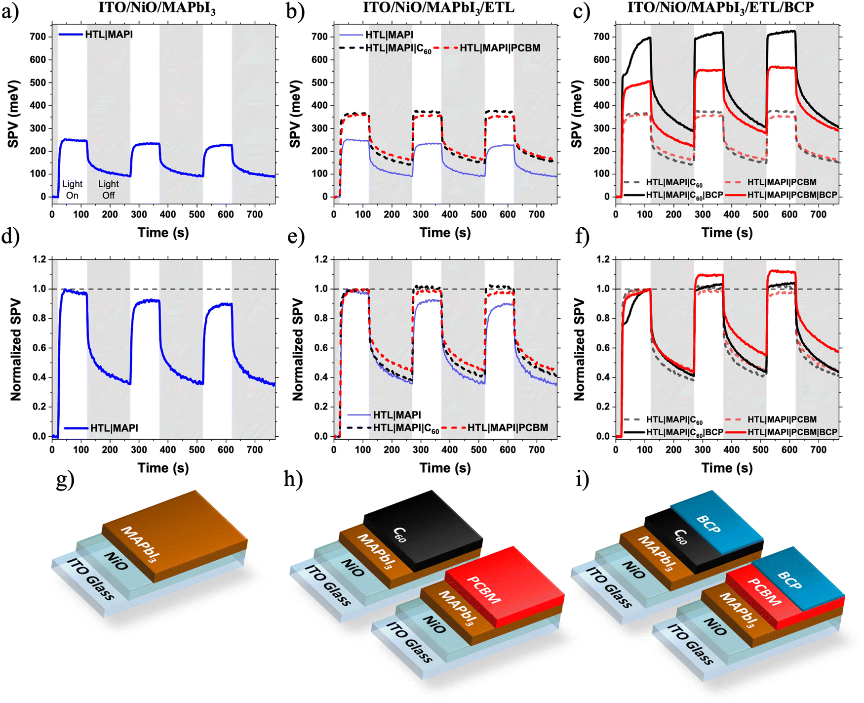 | ||
| Fig. 2 (a)–(c) Surface photovoltage plots, (d)–(f) normalised surface photovoltage plots and (g)–(i) corresponding sample structure diagrams. The white regions of the SPV plots indicate periods when the sample was illuminated (white light, 1/5 Sun), grey regions indicate periods the sample was not illuminated. | ||
There is a very little difference between the SPV responses of the ITO/NiO/MAPbI3/C60 and ITO/NiO/MAPbI3/PC61BM samples (Fig. 2b and e). The magnitude of SPV for both samples is similar (C60: 367 meV, PC61BM: 361 meV), consistent with the similar energetics of the two materials (Fig. S3, ESI†). Additionally, there are no significant differences in the SPV light turn-on or -off dynamics of the two samples, indicating similar slow photophysical processes such as charge trapping/de-trapping and/or chemical changes. This observation suggests that, in these devices, the perovskite/fullerene interface is not responsible for the observed LS effect in devices.
Surprisingly, upon addition of a very thin BCP layer (PC61BM/BCPsol-processed (10 nm), C60/BCPevaporated (5 nm)), the intensity of the SPV signal increases dramatically for both samples (C60/BCP: 696 meV, PC61BM/BCP: 506 meV at the end of the first illumination cycle). This suggests, in agreement with previous observations,34 that BCP is active (photophysically and/or energetically) in assisting efficient charge extraction from the fullerene layer, rather than simply acting as an insulating spacer layer between the ETL and Ag electrode. The reasons for the difference in SPV response magnitude between C60/BCP and PC61BM/BCP samples are discussed later. More importantly, there is a noticeable difference in the SPV dynamics during light on/off cycles (Fig. 2c and f). When the SPV intensities are normalised to their magnitude at the end of the first light-on cycle, a clear growth is observed in the PC61BM/BCP signal during further cycles, which is not observed in the C60/BCP signal. In the C60/BCP sample's SPV response, there is a fast increase observed in the first cycle, consistent with the small change in VOC at much shorter time scale in devices (Fig. S1, ESI†). However, the SPV signal of the C60/BCP sample stabilises much faster than the PC61BM/BCP, consistent with the rapid device LS shown in Fig. 1. To confirm if the differences in SPV response were due to the differing thicknesses or deposition methods of the BCP between the samples, the SPV response of an ITO/NiO/MAPbI3/PC61BM/BCPevaporated sample with BCP thickness of 5 nm was also measured (Fig. S4, ESI†). This sample showed similar SPV dynamics to the solution processed PC61BM/BCP sample, confirming that the PC61BM/BCP interface is responsible for the slow increase in SPV magnitude, matching with the slow LS effect observed in PC61BM/BCP devices.
To confirm the generality of this observation, devices and films with the MAPbI3 layer replaced with CsxFA1−xPbI3 were also fabricated. Again, the C60 based solar cells exhibited minimal light soaking behaviour and the PC61BM based solar cells exhibited strong light soaking behaviour (Fig. S5, ESI†). The same SPV experiment was performed. Although the CsxFA1−xPbI3 SPV shows much slower SPV response than MAPbI3 with the signal strength not saturating even after 100 s of illumination, a similar trend of slower SPV growth in the CsxFA1−xPbI3/PC61BM/BCP sample than in the CsxFA1−xPbI3/PC61BM sample being observed (Fig. S6, ESI†). In contrast, the CsxFA1−xPbI3/C60 and CsxFA1−xPbI3/C60/BCP samples’ SPV responses are much faster – similar to the SPV responses of the MAPbI3 samples shown in Fig. 2. This fast SPV response can be indicative of the thermally evaporated C60 passivating defects at the perovskite surface, which remain un-passivated by solution deposited PC61BM.35 These defects also appear to contribute to light soaking, as demonstrated by the slower LS and SPV responses of the CsxFA1−xPbI3/PC61BM PSCs compared to the MAPbI3/PC61BM PSCs (Fig. 1 and Fig. S5, ESI†). Further discussion and analysis of the CsxFA1−xPbI3 SPV data can be found in the ESI.† In summary, it is still clear that addition of the BCP to the CsxFA1−xPbI3/PC61BM sample slows the rate of SPV signal growth (Fig. S6b, ESI†), confirming that the PC61BM/BCP interface contributes to light soaking independently of the of the PAL used.
Revealing the molecular origin of light soaking
To probe the origin of the unexpected but critical role of the fullerene/BCP interface in light soaking, C60 and PC61BM films with and without BCP were characterised in detail as a function of illumination time. Mixed component PC61BM:BCP and C60:BCP films were prepared by spin-coating from mixed PC61BM![[thin space (1/6-em)]](https://www.rsc.org/images/entities/char_2009.gif) andBCP 1:1 (by weight) solutions or by co-evaporation of C60 and BCP. Blended films (fullerene:BCP) were chosen over bilayers (fullerene/BCP) in order to maximise the interaction between the fullerene and BCP molecules. Raman spectroscopy was employed to probe the vibrational states of the fullerene cage in both neat and blended films (Fig. 3a and b). PC61BM and C60 show characteristic Raman peaks at 1466 cm−1 and 1471 cm−1 respectively, associated with the Ag cage breathing vibrational mode.36–39
andBCP 1:1 (by weight) solutions or by co-evaporation of C60 and BCP. Blended films (fullerene:BCP) were chosen over bilayers (fullerene/BCP) in order to maximise the interaction between the fullerene and BCP molecules. Raman spectroscopy was employed to probe the vibrational states of the fullerene cage in both neat and blended films (Fig. 3a and b). PC61BM and C60 show characteristic Raman peaks at 1466 cm−1 and 1471 cm−1 respectively, associated with the Ag cage breathing vibrational mode.36–39
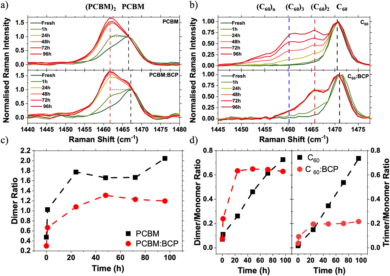 | ||
| Fig. 3 Raman spectra using 785 nm excitation of neat and blended fullerene films following 1 Sun illumination under N2. (a) Normalised Raman spectra of PC61BM (top) and PC61BM:BCP (bottom) films over 96 hours of 1 Sun illumination, (b) normalised Raman spectra of C60 (top) and C60:BCP (bottom) films over 96 hours of 1 Sun illumination. Raman spectra are normalised to the intensity of the higher energy, monomer peak. (c) Evolution of the dimer/monomer peak area ratio (i.e. a value of 1 indicates that monomer and dimer signals are of equal strength) for PC61BM (black) and PC61BM:BCP (red), (d) evolution of the dimer/monomer (left) and trimer/monomer peak area ratios for C60 (black) and C60:BCP (red). | ||
To simulate the light soaking in devices, films were exposed to 1 Sun conditions in an N2 atmosphere. Following illumination, the PC61BM spectrum shows the growth of a side peak at 1462 cm−1 (Fig. 3a, red dashed line), which is assigned to the formation of fullerene dimers via a [2+2] cycloaddition reaction by our DFT calculations (Fig. S8, ESI†) and existing literature.37 Upon blending the PC61BM with BCP the growth of a dimer side peak is also observed upon LS under 1 Sun conditions. By deconvoluting the contributions of the lower energy dimer signal and the higher energy monomer signal the relative ratios of the two species present can be quantified (see Fig. S10 for details, ESI†). In fresh samples the deconvoluted monomer:dimer ratio is 68:32 in the neat PC61BM and 77:23 in PC61BM:BCP film. Upon 1 Sun illumination, the rate of growth of the dimer side peak is slowed in the PC61BM:BCP blend film, with the final quantity of dimer being reduced by 40% in the blend compared to the neat PC61BM film. Illumination of films in an N2 atmosphere under 1 Sun followed by accelerated aging under 365 nm UV light shows the suppression of an optical absorption peak at 268 nm, coupled with an increase in absorption at around 320 nm (Fig. S9, ESI†). This observation is widely reported in the literature for neat PC61BM and is attributed to the formation of PC61BM dimers.37,40–42 These absorption changes are reduced in the PC61BM:BCP films compared to the neat PC61BM film, consistent with our Raman data and with previous observations.43 This data indicates that PC61BM is stabilised towards photoinduced changes (i.e. photodimerisation) by blending with BCP.
Photodimerisation is also known to occur between C60 molecules.44,45 Much of the work on photodimerisation of PC61BM has been driven by interest in its use as the acceptor phase in OPVs. However, due to C60's low solubility it has seen more limited use in OPV devices, and consequently literature on its photostability in photovoltaic devices is very limited. Fig. 3b shows the evolution of Raman spectra of evaporated C60 and co-evaporated C60:BCP blend films during following 1 Sun illumination in an N2 atmosphere. In the C60 Raman spectrum the growth of a low energy shoulder peak at 1466 cm−1 (red dashed line) is also observed upon illumination. This energy down-shift in the Ag peak is again associated with the formation of C60/C60 dimers (Fig. S7, ESI†).44,46 Oppositely to PC61BM, the growth of the dimer side peak is accelerated in the C60:BCP blend film as compared to the neat film (Fig. 3d). This acceleration occurs over short time scales, with the changes in the C60:BCP blend film spectra saturating at 60% dimer to monomer ratio after 24 h of light soaking. In contrast, in the neat C60 film the changes continue, although at a slower rate, for the full 96 h of light soaking without saturating and exceeding the percentage of dimer formed in the blend films. Additionally, a third peak at 1461 cm−1 (blue dashed line) is evident in the neat film, which is not observed in the C60:BCP blend. This peak at much lower energy is attributed to the formation of trimers (Fig. S8, ESI†).47 Therefore, in contrast to PC61BM, BCP promotes the formation of C60 dimers but suppresses the formation of longer oligomers. At short illumination timescales (∼1 h) little change is observed in the neat C60 film absorption – even after additional accelerated aging under a 365 nm UV light (Fig. S9, ESI†). In contrast, the C60:BCP blend film shows a significant decrease in the absorption maximum at 265 nm upon aging. This supports the interpretation of the Raman spectra and confirms that the photodimerisation rate of C60 is increased upon blending with BCP.
Increased Raman intensity in the 1450–1455 cm−1 region of the neat C60 spectra (Fig. 3b) suggests that longer chain oligomers or photopolymers are also formed under continuous illumination. This side peak growth can be most clearly seen in the increase of the unfitted area of Fig. S10c (ESI†). This is confirmed by comparison of the solubility of photoaged C60 and C60:BCP films in toluene. As shown in Fig. S14 (ESI†) neat C60 films exhibit very poor solubility, whereas the photoaged C60:BCP films dissolve readily, leaving no observable residue44,45 This observation confirms that oligomers are formed in the neat C60 films upon photoaging, compared to mainly dimers (expected to be much more soluble) in the C60:BCP films.
To further confirm the presence of dimers, high-pressure liquid chromatography (HPLC) measurements were performed with solutions prepared by dissolving fresh and photoaged films in toluene (Fig. S11, ESI†). The intensity of absorption at the retention time of the dimers is suppressed in the PC61BM:BCP blend film. By comparing the integrated areas of the monomer and dimer absorption peaks, the dimer:monomer can be quantified. Following aging for 24 h the dimer ratio is reduced by 7% in the blend compared to the neat sample, increasing to a 19% reduction after 96 h (Fig. S12, ESI†). This data supports the analysis of the Raman and absorption spectra, that BCP stabilises PC61BM by reducing the rate at which photodimerisation occurs. Further discussion of the HPLC analyses, including on C60 films, can be found in the ESI.†
To explain these observations, we first discuss the important role of BCP in stabilising PC61BM against photoinduced changes. This brings us to one of BCP's key properties, its chelating behaviour. BCP is known to interact strongly with metal atoms and ions as a bidentate ligand via the two nitrogen lone pairs on its pyridyl rings, enabling gap state formation.15,48,49 Additionally, BCP is also thought to donate electron density to electron deficient organic molecules such as PC61BM.43,50 For example, Hang et al. observed that a BCP analogue, Bphen, stabilises PC61BM against light induced degradation when applied as an interlayer at the SnO2/perovskite interface in an n–i–p PSC.43 The stabilisation of PC61BM by Bphen is attributed to donation of lone pair electron density from the pyridyl group to the fullerene cage, forming a charge transfer (CT) complex. As BCP differs from Bphen only in the presence of a methyl group at the ortho position of the pyridine ring, it is reasonable to conclude that the mechanism of stabilisation (i.e. charge-transfer (CT) complex formation) is similar in both systems. We observe a small (∼1 cm−1) upshift in both the PC61BM and C60 Raman peaks upon blending with BCP (Fig. 4a). This shift has previously been assigned to the BPhen/BCP CT complex with fullerenes, with increased electron density on the cage resulting in an increased effective force constant of the vibrational mode.43,50,51 Further evidence for this interaction is given by the Raman spectra shown in Fig. 4b. BCP has characteristic Raman peaks at 1371 cm−1 (peak 1, intra pyridine ring C–C stretch) and 1607 cm−1 (peak 2, phenyl intra ring C–C stretch) respectively (Fig. S15 and Table S2, ESI†). Upon blending with C60 there is a dramatic reduction in the Raman intensity of the pyridine peak relative to the phenyl peak. This reduction in relative Raman activity implies that electron density is being donated from the pyridyl rings in BCP onto the C60, confirming BCP/C60 CT complex formation. Electrostatic potential (ESP) maps of C60 and BCP calculated for different intermolecular spacings visualises such donation of electron density from the BCP pyridyl groups onto the C60 cage when two molecules are in close proximity (Fig. S16, ESI†). Calculated Raman spectra of C60, BCP and the C60/BCP CT complex shown in Fig. S16 (ESI†) are given in Fig. S17 (ESI†). The simulated Raman spectra match the experimental spectra closely, supporting the conclusion that CT complex formation between fullerene and BCP is confirmed the presented Raman data.
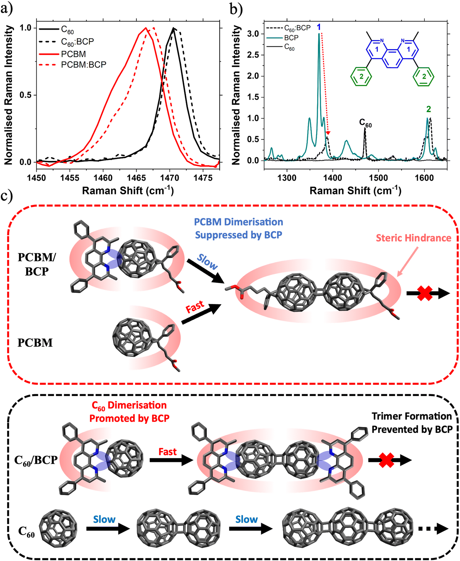 | ||
| Fig. 4 Molecular origin of light soaking effect. (a) Raman spectra of C60 (black) and PC61BM (red) films and corresponding BCP blend films (dashed); (b) normalised Raman spectra of fresh C60:BCP (black, dashed), BCP (blue) and C60 (black) films (normalisation to peak 2); (c) illustrative diagram outlining the proposed mechanism by which BCP increases the rate of C60 dimerisation but reduces the rate of PC61BM dimerisation. | ||
Based on our observations, we believe the rate of photodimerisation is affected differently for the two different fullerene:BCP CT complexes. In the case of PC61BM, blending with BCP suppresses the formation of fullerene/fullerene dimers. Whereas upon blending C60 with BCP, dimerisation is accelerated while the formation of trimers and other oligomers is suppressed. This can be understood with reference to the molecular structures of the two fullerenes. As discussed, the lone pairs on the BCP nitrogen groups donate electron density onto the electron deficient fullerene cage, forming a CT complex. This increased electron density may promote the formation of fullerene/fullerene dimers via a [2+2] cycloaddition mechanism. This explains the observation of increased dimerisation rates in the C60:BCP films, compared to the neat C60. Once a (C60)2 dimer has formed, BCP is expected to preferentially arrange itself (due to steric interactions) at either end of the dimer as shown in Fig. 4c, effectively capping the molecule, and preventing longer oligomer formation. Furthermore, we expect that the dimerisation is likely to occur at the side of the fullerene furthest from the BCP for steric reasons. Similarly further reactions of the dimer to afford trimers or oligomers will be supressed because of the steric blocking effect of the BCP group. In contrast, the rate of dimer formation is lower in neat C60 (due to lack of electron density donation from BCP) but the formation of trimers and higher-order oligomers is no longer sterically hindered and proceeds uninterrupted. In contrast, due to the steric impact of the bulky solubilising side group on PC61BM the BCP can be expected to arrange itself trans to this group, sterically hindering the PC61BM dimerisation reaction and reducing its rate. Whereas in the neat PC61BM film the side group only sterically hinders the cycloaddition reaction once a dimer has formed, preventing the formation of trimers. This is supported by the work of Distler et al., which showed that by replacing PC61BM with bis-PC61BM (a bis-subsituted analogue of PC61BM) fullerene/fullerene dimerisation was suppressed by steric hindrance.40 In this case we have only considered the trans isomer of the PC61BM dimer, however with other isomers (such as those reported by Pont et al.)52 the effect of BCP is expected to be similar.
The photochemical processes described above are expected to occur at the fullerene/BCP interfaces in the devices. To correlate these processes to the device light soaking effect, we undertook further work to understand their effect on the energetic landscape and device physics within the PSCs. Using DFT simulations we first calculated the effect of fullerene dimerisation on the energies of the frontier molecular orbitals. Upon dimerisation the simulated HOMO levels raise by 0.21 eV and 0.13 eV for C60 and PC61BM respectively, with a corresponding deepening of the LUMO levels (Fig. S19, ESI†). Additionally, a further HOMO level shallowing of 0.06 eV is found upon conversion of a C60 dimer into a trimer. These changes in HOMO/LUMO levels lead to the narrowing of fullerene band gaps upon dimerisation, which are in good agreement with the absorption data (Fig. S9, ESI†). The deeper LUMO levels in dimers will lead to barrierless electron transport from fullerene monomers to dimers. Our observations above show that BCP will accelerate C60 dimer formation at the C60/BCP interface upon illumination. Therefore, this will result in a favourable cascading energetic landscape for efficient electron transport towards the C60/BCP interface, caused by a higher concentration of dimers at this interface. The C60/perovskite interface is known to be a key site of energetic loss due to recombination at C60 trap states.53 The cascading electron transport mechanism will reduce the accumulation of electrons in traps states at the perovskite/C60 interface and hence interfacial recombination at this interface. This is consistent with the rapid rise in SPV and VOC observed upon initial illumination. In contrast, in the PC61BM/BCP system, dimerisation at this interface is suppressed, so cannot gain the cascading energetic benefit as photodimer concentration will be higher in the PC61BM bulk. This leads us to conclude that PC61BM dimerisation cannot be the cause of slow light soaking observed in devices.
Next, we discuss the impact of fullerene/BCP CT complex formation on device energetic landscape. We find evidence for new electronic states associated with fullerene/BCP CT complexes in the ambient photoemission spectra (APS) in Fig. 5a and b. A shallowing of the measured HOMO levels by 110 meV for both C60 and PC61BM is observed upon blending with BCP. The APS response of neat BCP occurs at deeper energies than the neat fullerene films, so the HOMO level shallowing of C60 and PC61BM cannot be attributed to contributions from BCP's molecular orbitals. Therefore in this case we interpret this HOMO shift to lower energies as further evidence for the formation of fullerene/BCP CT complexes, similar to those reported for Ag/BCP.16,21 Whilst APS probes the HOMO energy level, studies on BCP/metal complexes have shown concurrent HOMO shallowing and LUMO deepening upon complex formation.15,20 This leads us to conclude that fullerene/BCP CT complexes will also possess LUMO levels deeper than neat BCP. Both PC61BM:BCP and C60:BCP films exhibit further shallowing in measured HOMO level upon light soaking for 10 minutes under 1 Sun conditions in N2, whilst the neat films show smaller changes (Fig. 5a and b insets). In the C60:BCP film the C60 HOMO shallows by 55 meV whilst in the PC61BM:BCP film the PC61BM HOMO level shifts by 170 meV, suggesting more significant electron density transfer from BCP to PC61BM during LS, highlighting stronger photo-induced CT complex formation for PC61BM compared to C60. By integrating the area below the HOMO edge of the APS spectra of both PC61BM:BCP and C60:BCP films before and after LS, the impact of CT complex formation on trap state density is assessed (Fig. S20, ESI†).54–56 A 30% increase in the tail state area of the PCBM:BCP spectrum is observed upon LS, this is compared to a 9% decrease in the tail state area of the C60:BCP spectrum. This may explain the reduced SPV magnitude of the PCBM/BCP partial device sample compared to the C60/BCP sample (Fig. 2c), with the shallow PCBM/BCP gap states acting as shallow trap sites. This however does not seem to have large impact on final device performance.
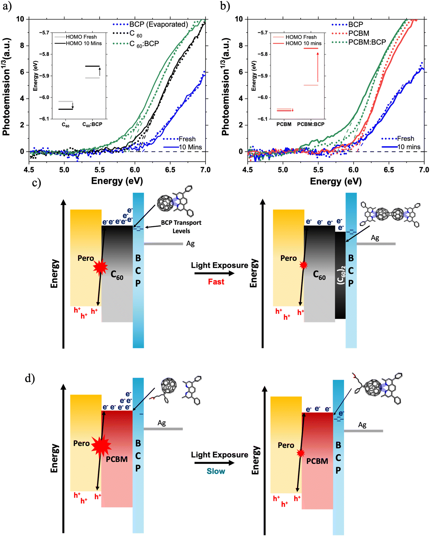 | ||
| Fig. 5 The effect of light soaking on energetics at the fullerene:BCP interface. APS spectra of (a) C60 and (b) PC61BM films with and without BCP before and after 10 minutes exposure to 1 Sun conditions under N2. Inset charts in (a) and (b) show the fitted HOMO levels before and after 10 min LS. Diagrams of proposed energetic changes in (c) C60 and (d) PC61BM based PSCs under light soaking. | ||
Overall, the APS data suggests that the C60/BCP CT complex is predominantly formed spontaneously upon BCP deposition and LS moderately improves the interfacial properties by slightly reducing trap state density. In contrast, for PC61BM/BCP, only a modest amount of CT complex is formed spontaneously but this is significantly enhanced by light soaking, highlighting the sensitivity of PC61BM/BCP CT complex formation towards light. Additionally, formation of the CT complex in PC61BM:BCP during LS is associated with the formation of new energetic states and is strongly coupled with a large increase in the sub-gap trap state, suggesting a significant increase in energetic disorder at the PC61BM/BCP interface.54,57,58 Therefore, we propose that the slow formation of these PC61BM/BCP CT complexes under illumination is the main cause of the slow LS effect observed in the PC61BM containing PSCs.
Conclusions
In conclusion, we have isolated a light soaking effect in large area perovskite solar cells to the fullerene/BCP interface using SPV. This effect is independent of the perovskite photoactive layer used. We have shown that the molecular structure of the fullerene used (PC61BM vs. C60) causes dramatic differences to the rate of the fullerene/fullerene dimerisation in the presence of BCP. We have linked this behaviour to LS in devices by considering the energetic effects of dimerisation and investigation of the formation of CT complex states at the fullerene/BCP interface. We find that a thin layer of (C60)2 photodimers is formed rapidly under illumination at the interface between C60 and BCP which aids charge extraction to the BCP – moderately reducing recombination loss across the perovskite/C60 interface and leading to a small, fast increase in the device VOC upon LS. In contrast, in the PC61BM devices LS cannot be attributed to dimer formation at the PC61BM/BCP interface due to suppression of PC61BM dimerisation by BCP. Instead, we find that new energetic states associated with light induced PC61BM/BCP CT complex formation are essential for efficient charge transport from PC61BM to BCP. These BCP CT complexes predominantly form spontaneously with C60 but not with PC61BM, perhaps due to the same steric effects which affect dimerisation rate. This light induced CT complex formation is evidenced by the shallowing of the measured HOMO level in the PC61BM:BCP film upon LS. Therefore, we propose that the slow formation of PC61BM/BCP CT complexes under illumination is the cause of the slow LS effect observed in the PSCs.This study provides important insight into the role of the widely used fullerene/BCP electron transport system in perovskite solar cells and demonstrates that the optimisation of non-perovskite interfaces in devices is critical for further development of PSCs. As increasing effort is being put into using non-fullerene ETMs (with greater opportunity for chemical, and therefore energetic, modification) in p–i–n PSCs, the role of BCP in charge extraction will come under greater scrutiny because the majority of reported fullerene-free p–i–n PSCs still use BCP (or another interlayer) between the ETL and cathode.59 Therefore, the design of new ETMs must take the role of BCP in devices into account.
Methods
Large-area perovskite solar cell and sample fabrication
Perovskite devices and samples were fabricated in a cleanroom in air at relative humidity in the range 30–50% using an Erichsen 510 blade coater. 50 mm × 50 mm pre-patterned glass/ITO substrates (10 Ω sq−1, Thin Film Devices Inc.) were cleaned in an ultrasonic bath sequentially in aqueous detergent, de-ionised water, acetone and finally isopropanol. The substrates were dried under N2 flow and treated by UV/O3 (NovaScan PSD 4) for 15 minutes. After substrate cleaning, the NiOx solution (nanoparticle solution with initial concentration of 2.5% and diluted in 1:5 in ethanol) was immediately blade coated using a gap of 575 μm and speed of 5 mm s−1; the resulting film was annealed under an IR lamp for 2 min and after in UVO3 for 2.5 min. The perovskite precursor ink was formed from Pb(C2H3O2)2, PbCl2 and CH3NH3I with a molar ratio of 0.8:0.2:2.9 in DMF. Perovskite films were deposited by blade coating with a gap of 100 μm and speed of 10 mm s−1 at 43 °C, and the resulting wet film was dried with a nitrogen flow by a custom N2 knife developed by Oninn. Samples were then transferred to a hot plate for annealing at 100 °C for 30 min. CsxFA1−xPbI3 perovskite films were fabricated using the method described above for MAPbI3, with the precursor solution containing CsI, FAI and PbI2 in a 0.17:0.83:1 molar ratio in DMF, to give a final composition of Cs0.18FA0.83PbI3. PCBM (Nano-C, 99.82%) solutions (20 mg mL−1, o-xylene) was deposited by blade coating with a speed of 10 mm s−1 and a gap of 125 μm. C60 (Nano-C, 99.88%) was deposited by vacuum evaporation (20 nm, 0.2 Å s−1, pressure <5 × 10⁻⁶ mbar). BCP (TCI, >95%) was deposited from solution (isopropanol, 0.5 mg mL−1) by blade coating with a gap of 100 μm at 5 mm s−1 for PCBM devices or by vacuum evaporation (5 nm, 0.2 Å s−1, pressure <5 × 10⁻⁶ mbar) for C60 devices. Silver back electrodes were deposited by vacuum evaporation at pressures <5 × 10⁻⁶ mbar using a shadow mask to define eight cells with an active area of 0.5 cm2 each.
Large area devices of size 5 × 5 cm, with 0.5 cm2 pixels allow for 8 cells to be formed on each substrate. This has two key advantages: firstly, this enables more statistical data to be generated per substrate. The second, more important, aspect is to enable the uniformity of the coating to be understood. This allows for the stack and deposition methods to be validated, with the vision of having sufficient quality for the construction of large area modules.
Partial device stacks used for energetic characterisation were fabricated according to the steps described above, without the deposition of subsequent layers as required by the final sample structure.
Fullerene and fullerene:BCP blend films were deposited on quartz (for absorption and Raman) or ITO glass (for APS and Kelvin probe). PCBM and 50:50 (wt) PCBM:BCP blend films were deposited from solution (chlorobenzene, 15 mg mL−1) by spin coating. C60 and 50:50 (thickness) C60:BCP blend films were deposited by (co-)evaporation in a Kurt J. Lesker SPECTROS 100 system with a base pressure 10−7 mbar. Quartz crystal microbalances were used to precisely control the deposition rates and thickness of thin films. Films of thickness 200 nm (for Raman) and 100 nm (for APS and absorption spectra) were grown at a total deposition rate of 0.5 Å s−1, from a single source, or two simultaneously in the case of blend films.
Photovoltaic characterisation
Current–voltage (J–V) characteristics of PSCs were collected under 1 Sun (AM 1.5G) illumination in N2. No pre-biasing or light soaking was performed on the devices prior to testing. Pixels (0.5 cm2, ×8 per device) were scanned sequentially with a step of 0.01 V and a scan rate of 0.4 V s−1.Energetic measurements and surface photovoltage (SPV)
Ambient photoemission spectroscopy and (APS) and SPV and dark work function (DWF) measurements were performed using a KP Technology APS04 system. DWF measurements were performed first, followed by SPV and finally APS; this was done to reduce the effect of any UV light induced degradation processes on other measurements. DWF and SPV measurement utilised a Kelvin probe (∅: 2 mm, Au) fitted with an off-null system,60 calibrated using the contact potential difference (CPD) and APS response of a freshly cleaned Ag reference. SPV was performed using cycled broad band (800–400 nm) white light illumination of intensity 1/5 Sun from a quartz tungsten lamp, with simultaneous CPD measurement. SPV and DWF data was collected with measurement rate of 0.8 Hz. APS spectra were collected using a UV lamp fitted with a monochromator, with photon energies incident on the sample being varied from 4.5 to 6.8 eV. Photogenerated electrons were collected using the Kelvin probe tip biased at 10 V.61 HOMO levels were fitted using the linear region of the cube root of the photoemission (PE) generated current.Raman spectroscopy
Raman spectra were collected using a Renishaw inVia Raman microscope in backscattering mode, with the sample located within a Linkam stage under continuous flowing N2. A 785 nm diode laser, defocused by 25% to reduce sample degradation, performed the excitation. Raman spectra were collected from a minimum of 21 different sites on each sample, with the mean of these spectra being reported. No spectral changes were observed following exposures of the same sample site to the 785 nm laser for any film, ruling out laser induced degradation as a cause for our observations. Spectrometer calibration was performed using an Si reference and the PL background was subtracted using a polynomial fit. To aid visual interpretation, Raman spectra of PCBM and PCBM:BCP films were smoothed using a Savitzky–Golay filter with a window length of 6.Simulations
Density functional theory (DFT) simulations were carried out on the Imperial College High Performance Computing service using Gaussian16 and results were visualised using GaussView 6.0.17. Simulations were performed on single molecules in the gas phase at the B3LYP (hybrid) level of theory using the 6-311G(d,p) basis set. Molecular structures were optimised to their minimum energies before Raman vibrational modes were calculated. To compare with experimental Raman spectra, a scaling factor of 0.97 was applied to the simulated Raman frequencies.62 ESP maps were performed as single point calculations (i.e. molecular geometry was optimised for isolated molecules, with the ESP of C60/BCP pairs being calculated without further geometry optimisation).High performance liquid chromatography
High performance liquid chromatography (HPLC) was performed on an Agilent 1100 apparatus consisting of an G1322A degasser, G1311A quaternary pump, G1313A ALS, G1315B diode array detector (Agilent, USA) with an analytical COSMOSIL BUCKYPREP column (4.6 mm × 250 mm) and mobile phase toluene with a flow rate of 1.5 mL min−1. Films were dissolved off substrates in toluene and filtered through a 0.2 μm PTFE syringe filter and 20 μL injected into the system. The diode array detector was set to two wavelengths, 290 nm and 340 nm.Author contributions
C. H. conceived the study, performed APS, Kelvin probe, SPV and Raman measurements, performed DFT calculations, analysed data and prepared the first draft of the manuscript. J. L. prepared neat and blend PC61BM and PC61BM:BCP films, assisted with experimental design, data analysis, and the first draft of the manuscript. I. S. B. and L. C. fabricated and tested the large area printed PSCs under the supervision of D. B. E. J. Y. performed DFT calculations on fullerene dimers and trimers and validated other DFT results. M. R. performed and analysed the HPLC under the supervision of M. H. and N. G. H. D. prepared the neat and blend C60 and C60:BCP films under the supervision of S. H. Y. C. C. and T. L. assisted with the validation and interpretation of APS, Kelvin probe and SPV data. J. S. K conceived the study and supervised the whole project, directed/revised the manuscript, and procured funding. All authors contributed to the discussion of results and final version of the manuscript.Conflicts of interest
There are no conflicts to declare.Acknowledgements
C. H. acknowledges the UK EPSRC for DTP studentship and Oninn for CASE studentship support. This research was supported by the EPSRC ATIP Programme Grant (EP/T028513/1). I. S. B, C. L. and D. B. acknowledge CEMIG (Companhia Energética de Minas Gerais S. A.) for financial support (04951-0660/2022 – ANEEL). The authors thank Chiara Labanti for her assistance with sample fabrication.References
- J. Park, J. Kim, H.-S. Yun, M. J. Paik, E. Noh, H. J. Mun, M. G. Kim, T. J. Shin and S. Il Seok, Nature, 2023, 616, 724–730 CrossRef CAS PubMed.
- L. Lin, L. Yang, G. Du, X. Li, Y. Li, J. Deng, K. Wei and J. Zhang, ACS Appl. Energy Mater., 2023, 6 DOI:10.1021/acsaem.2c04120.
- S. Shao and M. A. Loi, Adv. Mater. Interfaces, 2020, 7, 1901469 CrossRef CAS.
- C. Zhao, B. Chen, X. Qiao, L. Luan, K. Lu and B. Hu, Adv. Energy Mater., 2015, 5, 1500279 CrossRef.
- J. Hu, R. Gottesman, L. Gouda, A. Kama, M. Priel, S. Tirosh, J. Bisquert and A. Zaban, ACS Energy Lett., 2017, 2, 950–956 CrossRef CAS.
- S. Shao, M. Abdu-Aguye, L. Qiu, L.-H. Lai, J. Liu, S. Adjokatse, F. Jahani, M. E. Kamminga, G. H. ten Brink, T. T. M. Palstra, B. J. Kooi, J. C. Hummelen and M. Antonietta Loi, Energy Environ. Sci., 2016, 9, 2444–2452 RSC.
- J. Luke, L. Corrêa, J. Rodrigues, J. Martins, M. Daboczi, D. Bagnis and J. Kim, Adv. Energy Mater., 2021, 11, 2003405 CrossRef CAS.
- M. M. Lee, J. Teuscher, T. Miyasaka, T. N. Murakami and H. J. Snaith, Science, 2012, 338, 643–647 CrossRef CAS PubMed.
- X. Lin, D. Cui, X. Luo, C. Zhang, Q. Han, Y. Wang and L. Han, Energy Environ. Sci., 2020, 13, 3823–3847 RSC.
- S. Zhang, F. Ye, X. Wang, R. Chen, H. Zhang, L. Zhan, X. Jiang, Y. Li, X. Ji, S. Liu, M. Yu, F. Yu, Y. Zhang, R. Wu, Z. Liu, Z. Ning, D. Neher, L. Han, Y. Lin, H. Tian, W. Chen, M. Stolterfoht, L. Zhang, W. Zhu and Y. Wu, Science, 2023, 380, 404–409 CrossRef CAS PubMed.
- Q. Tan, Z. Li, G. Luo, X. Zhang, B. Che, G. Chen, H. Gao, D. He, G. Ma, J. Wang, J. Xiu, H. Yi, T. Chen and Z. He, Nature, 2023, 32–34 CAS.
- H. Gommans, B. Verreet, B. P. Rand, R. Muller, J. Poortmans, P. Heremans and J. Genoe, Adv. Funct. Mater., 2008, 18, 3686–3691 CrossRef CAS.
- R. Tomova, P. Petrova and R. Stoycheva-Topalova, Phys. Status Solidi C, 2010, 7, 992–995 CrossRef CAS.
- Y. Bai, X. Meng and S. Yang, Adv. Energy Mater., 2018, 8, 1701883 CrossRef.
- H. Yoshida, J. Phys. Chem. C, 2015, 119, 24459–24464 CrossRef CAS.
- Y. Nakayama, T. L. Nguyen, Y. Ozawa, S. Machida, T. Sato, H. Tokairin, Y. Noguchi and H. Ishii, Adv. Energy Mater., 2014, 4, 1301354 CrossRef.
- C. Chen, S. Zhang, S. Wu, W. Zhang, H. Zhu, Z. Xiong, Y. Zhang and W. Chen, RSC Adv., 2017, 7, 35819–35826 RSC.
- M. Vogel, S. Doka, C. Breyer, M. C. Lux-Steiner and K. Fostiropoulos, Appl. Phys. Lett., 2006, 89, 163501 CrossRef.
- B. R. Patil, M. Ahmadpour, G. Sherafatipour, T. Qamar, A. F. Fernández, K. Zojer, H.-G. Rubahn and M. Madsen, Sci. Rep., 2018, 8, 12608 CrossRef PubMed.
- J. Lee, S. Park, Y. Lee, H. Kim, D. Shin, J. Jeong, K. Jeong, S. W. Cho, H. Lee and Y. Yi, Phys. Chem. Chem. Phys., 2016, 18, 5444–5452 RSC.
- G. H. Jung and J.-L. Lee, J. Mater. Chem. A, 2013, 1, 3034 RSC.
- H. Lee, G. Cho, S. Woo, S. Nam, J. Jeong, H. Kim and Y. Kim, RSC Adv., 2012, 2, 8762 RSC.
- D. Burkitt, R. Patidar, P. Greenwood, K. Hooper, J. McGettrick, S. Dimitrov, M. Colombo, V. Stoichkov, D. Richards, D. Beynon, M. Davies and T. Watson, Sustainable Energy Fuels, 2020, 4, 3340–3351 RSC.
- D.-K. Lee and N.-G. Park, Sol. RRL, 2022, 6, 2100455 CrossRef CAS.
- Y. Wang, C. Duan, P. Lv, Z. Ku, J. Lu, F. Huang and Y.-B. Cheng, Natl. Sci. Rev., 2021, 8 DOI:10.1093/nsr/nwab075.
- S. Castro-Hermosa, L. Wouk, I. S. Bicalho, L. de Queiroz Corrêa, B. de Jong, L. Cinà, T. M. Brown and D. Bagnis, Nano Res., 2021, 14, 1034–1042 CrossRef CAS.
- M. Daboczi, I. Hamilton, S. Xu, J. Luke, S. Limbu, J. Lee, M. A. McLachlan, K. Lee, J. R. Durrant, I. D. Baikie and J.-S. Kim, ACS Appl. Mater. Interfaces, 2019, 11, 46808–46817 CrossRef CAS PubMed.
- L. Kronik and Y. Shapira, Surf. Interface Anal., 2001, 31, 954–965 CrossRef CAS.
- M. Daboczi, J. Kim, J. Lee, H. Kang, I. Hamilton, C. Lin, S. D. Dimitrov, M. A. McLachlan, K. Lee, J. R. Durrant and J. Kim, Adv. Funct. Mater., 2020, 30, 2001482 CrossRef CAS.
- M. Daboczi, S. R. Ratnasingham, L. Mohan, C. Pu, I. Hamilton, Y.-C. Chin, M. A. McLachlan and J.-S. Kim, ACS Energy Lett., 2021, 6, 3970–3981 CrossRef CAS.
- Y.-C. Chin, M. Daboczi, C. Henderson, J. Luke and J.-S. Kim, ACS Energy Lett., 2022, 7, 560–568 CrossRef CAS PubMed.
- F. Zu, C. M. Wolff, M. Ralaiarisoa, P. Amsalem, D. Neher and N. Koch, ACS Appl. Mater. Interfaces, 2019, 11, 21578–21583 CrossRef CAS PubMed.
- N. Aristidou, I. Sanchez-Molina, T. Chotchuangchutchaval, M. Brown, L. Martinez, T. Rath and S. A. Haque, Angew. Chem., Int. Ed., 2015, 54, 8208–8212 CrossRef CAS PubMed.
- M. Sakomura, Y. Yokokura, Y. Takagi and K. Ueda, AIP Adv., 2020, 10, 015144 CrossRef CAS.
- P.-W. Liang, C.-C. Chueh, S. T. Williams and A. K.-Y. Jen, Adv. Energy Mater., 2015, 5, 1402321 CrossRef.
- A. Dzwilewski, T. Wågberg and L. Edman, J. Am. Chem. Soc., 2009, 131, 4006–4011 CrossRef CAS PubMed.
- Z. Li, H. C. Wong, Z. Huang, H. Zhong, C. H. Tan, W. C. Tsoi, J. S. Kim, J. R. Durrant and J. T. Cabral, Nat. Commun., 2013, 4, 2227 CrossRef PubMed.
- D. S. Bethune, G. Meijer, W. C. Tang and H. J. Rosen, Chem. Phys. Lett., 1990, 174, 219–222 CrossRef CAS.
- T. J. Dennis, J. P. Hare, H. W. Kroto, R. Taylor, D. R. M. Walton and P. J. Hendra, Spectrochim. Acta, Part A, 1991, 47, 1289–1292 CrossRef.
- A. Distler, T. Sauermann, H.-J. Egelhaaf, S. Rodman, D. Waller, K.-S. Cheon, M. Lee and D. M. Guldi, Adv. Energy Mater., 2014, 4, 1300693 CrossRef.
- S. Pont, J. R. Durrant and J. T. Cabral, Adv. Energy Mater., 2019, 9, 1803948 CrossRef.
- T. Heumueller, W. R. Mateker, A. Distler, U. F. Fritze, R. Cheacharoen, W. H. Nguyen, M. Biele, M. Salvador, M. von Delius, H.-J. Egelhaaf, M. D. McGehee and C. J. Brabec, Energy Environ. Sci., 2016, 9, 247–256 RSC.
- P. Hang, J. Xie, C. Kan, B. Li, Y. Zhang, P. Gao, D. Yang and X. Yu, Adv. Mater., 2021, 33, 2006910 CrossRef CAS PubMed.
- Y. Wang, J. M. Holden, Z.-H. Dong, X.-X. Bi and P. C. Eklund, Chem. Phys. Lett., 1993, 211, 341–345 CrossRef CAS.
- A. M. Rao, P. Zhou, K.-A. Wang, G. T. Hager, J. M. Holden, Y. Wang, W.-T. Lee, X.-X. Bi, P. C. Eklund, D. S. Cornett, M. A. Duncan and I. J. Amster, Science, 1993, 259, 955–957 CrossRef CAS.
- S. Lebedkin, A. Gromov, S. Giesa, R. Gleiter, B. Renker, H. Rietschel and W. Krätschmer, Chem. Phys. Lett., 1998, 285, 210–215 CrossRef CAS.
- H. Chadli, A. Rahmani and J.-L. Sauvajol, J. Phys.: Condens. Matter, 2010, 22, 145303 CrossRef CAS PubMed.
- P. A. Forero Cortés, M. Marx, M. Trose and M. Beller, Chem Catal., 2021, 1, 298–338 CrossRef.
- D. Wang, A. B. Weinstein, P. B. White and S. S. Stahl, Chem. Rev., 2018, 118, 2636–2679 CrossRef CAS PubMed.
- T. Liu, L. Sun, C. Xie, W. Wang, F. Qin and Y. Zhou, J. Mater. Chem. A, 2021, 9, 23269–23275 RSC.
- S. Wood, J. Wade, M. Shahid, E. Collado-Fregoso, D. D. C. Bradley, J. R. Durrant, M. Heeney and J.-S. Kim, Energy Environ. Sci., 2015, 8, 3222–3232 RSC.
- S. Pont, S. Osella, A. Smith, A. V. Marsh, Z. Li, D. Beljonne, J. T. Cabral and J. R. Durrant, Chem. Mater., 2019, 31, 6076–6083 CrossRef CAS.
- J. Warby, F. Zu, S. Zeiske, E. Gutierrez-Partida, L. Frohloff, S. Kahmann, K. Frohna, E. Mosconi, E. Radicchi, F. Lang, S. Shah, F. Peña-Camargo, H. Hempel, T. Unold, N. Koch, A. Armin, F. De Angelis, S. D. Stranks, D. Neher and M. Stolterfoht, Adv. Energy Mater., 2022, 12, 2103567 CrossRef CAS.
- J. Wu, J. Lee, Y.-C. Chin, H. Yao, H. Cha, J. Luke, J. Hou, J.-S. Kim and J. R. Durrant, Energy Environ. Sci., 2020, 13, 2422–2430 RSC.
- C. Labanti, J. Wu, J. Shin, S. Limbu, S. Yun, F. Fang, S. Y. Park, C. Heo, Y. Lim, T. Choi, H.-J. Kim, H. Hong, B. Choi, K. Park, J. R. Durrant and J. Kim, Nat. Commun., 2022, 13, 3745 CrossRef CAS PubMed.
- Y. Fu, T. H. Lee, Y.-C. Chin, R. A. Pacalaj, C. Labanti, S. Y. Park, Y. Dong, H. W. Cho, J. Y. Kim, D. Minami, J. R. Durrant and J.-S. Kim, Nat. Commun., 2023, 14, 1870 CrossRef CAS PubMed.
- J. Marin-Beloqui, G. Zhang, J. Guo, J. Shaikh, T. Wohrer, S. M. Hosseini, B. Sun, J. Shipp, A. J. Auty, D. Chekulaev, J. Ye, Y.-C. Chin, M. B. Sullivan, A. J. Mozer, J.-S. Kim, S. Shoaee and T. M. Clarke, J. Phys. Chem. C, 2022, 126, 2708–2719 CrossRef CAS PubMed.
- S. Lee, D. Bin Kim, I. Hamilton, M. Daboczi, Y. S. Nam, B. R. Lee, B. Zhao, C. H. Jang, R. H. Friend, J.-S. Kim and M. H. Song, Adv. Sci., 2018, 5, 1801350 CrossRef.
- D. Wang, T. Ye and Y. Zhang, J. Mater. Chem. A, 2020, 8, 20819–20848 RSC.
- I. D. Baikie and P. J. Estrup, Rev. Sci. Instrum., 1998, 69, 3902–3907 CrossRef CAS.
- I. D. Baikie, A. Grain, J. Sutherland and J. Law, Phys. Status Solidi C, 2015, 12, 259–262 CrossRef CAS.
- M. L. Laury, M. J. Carlson and A. K. Wilson, J. Comput. Chem., 2012, 33, 2380–2387 CrossRef CAS PubMed.
Footnote |
| † Electronic supplementary information (ESI) available. See DOI: https://doi.org/10.1039/d3ee02571c |
| This journal is © The Royal Society of Chemistry 2023 |