
 Open Access Article
 This Open Access Article is licensed under a
 Creative Commons Attribution 3.0 Unported Licence
Design considerations for the bottom cell in perovskite/silicon tandems: a terawatt scalability perspective†
Matthew
Wright‡
 *a,
Bruno
Vicari Stefani‡
b,
Timothy W.
Jones
b,
Brett
Hallam
c,
Anastasia
Soeriyadi
a,
Li
Wang
c,
Pietro
Altermatt
a,
Henry J.
Snaith
d,
Gregory J.
Wilson
b and
Ruy Sebastian
Bonilla
a
*a,
Bruno
Vicari Stefani‡
b,
Timothy W.
Jones
b,
Brett
Hallam
c,
Anastasia
Soeriyadi
a,
Li
Wang
c,
Pietro
Altermatt
a,
Henry J.
Snaith
d,
Gregory J.
Wilson
b and
Ruy Sebastian
Bonilla
a
aDepartment of Materials, University of Oxford, Oxford, OX1 3PH, UK. E-mail: matthew.wright@materials.ox.ac.uk
bCSIRO Energy, Newcastle Energy Centre, 10 Murray Dwyer Circuit, Mayfield West NSW 2304, Australia
cSchool of Photovoltaic and Renewable Energy Engineering, The University of New South Wales, Kensington, NSW 2052, Australia
dClarendon Laboratory, Department of Physics, University of Oxford, Parks Road, Oxford, OX1 3PU, UK
First published on 25th August 2023
Abstract
Perovskite/silicon tandems have smashed through the 30% efficiency barrier, which represents a promising step towards high efficiency solar modules. However, the processing used to fabricate high efficiency devices is not compatible with mass production. For this technology to be impactful in the urgent fight against climate change and be scalable to the multi-terawatt (TW) level, a shift in mindset is required when designing the silicon bottom cell. In this work, we outline the design requirements for the silicon cell, with a particular focus on the constraints imposed by industrial processing. In doing so, we discuss the type of silicon wafers used, the surface treatment, the most appropriate silicon cell architecture and the formation of metal contacts. Additionally, we frame this discussion in the context of multi-TW markets, which impose additional constraints on the processing relating to the sustainability of the materials used. The discussion herein will help to shape the design of future silicon solar cells for use in tandems, so that the LCOE of solar electricity can be driven to new lows.
 Matthew Wright | Dr Matthew Wright received a PhD in Photovoltaic Engineering from UNSW Sydney in 2015. Following this, he was a postdoctoral fellow at UNSW Sydney, investigating the impact of illuminated annealing on silicon heterojunction solar cells. In 2021, he joined the electronic and interface materials laboratory at the University of Oxford. Dr Wright is a currently a Marie Skłodowska-Curie Postdoctoral Fellow at The University of Oxford, where he is working on the development of silicon bottom cells for perovskite/silicon tandem solar cells. |
 Bruno Vicari Stefani | Dr Bruno Vicari Stefani completed his PhD in Photovoltaic Engineering from UNSW Sydney in 2022, receiving a Dean's Award for Outstanding PhD theses. His PhD work focused on understanding light-induced degradation of silicon solar cells. He is currently a CERC Fellow at CSIRO, working on the development of silicon bottom cells for monolithic perovskite-on-silicon tandem solar cell applications. |
Broader contextSolar photovoltaics (PV) will play a crucial role in limiting global warming by replacing traditional fossil fuel generation. To transition the energy economy at the required rate to address climate change, a rapid expansion in the production of solar PV is needed in the coming decade. Crystalline silicon solar cells currently dominate the PV market. Over the past 20 years, the efficiency of industrial silicon solar cells has steadily improved, however, the technology is approaching a fundamental limit in performance. Perovskite/silicon tandem solar cells offer a pathway to overcome these limitations. Multiple groups have demonstrated efficiencies exceeding 30%, which is a massive achievement. However, some processing approaches and materials used in high efficiency tandem demonstrations are not compatible with mass production. To have a tangible impact on climate change, these high efficiency cells must be produced on a terawatt (TW) scale. In this work, we highlight the disconnect between current research techniques on perovskite/silicon tandem solar cells and the stringent constraints imposed by large scale mass manufacturing. By doing so, we highlight some of the critical design criteria that must be considered for this technology to become a commercial reality. |
1. Introduction
The urgent need to reduce CO2 emissions to mitigate the devastating impacts of climate change requires a rapid upscaling of solar photovoltaics (PV)1,2 Solar PV is increasingly used to replace electricity generation from fossil fuel sources and also for long-term storage via the formation of green hydrogen through electrolysis3–5 In 2021, a total global cumulative production of 191 GW of solar PV was manufactured, however, predictions suggest that this must expand to at least 1 TW (1000 GW) per year by 2030 to meet the Paris agreement6,7 Over the past 15 years, the cost of solar PV modules, as quantified in dollars per watt of power produced under peak sun light ($/Wp), has plummeted, reducing by a factor of 15 between 2008 and 2018.8 These cost reductions have been driven partly by technological advancements in both manufacturing and design, partly by scaling effects, and partly by moving most of the supply chain and manufacturing to China.9 This rapid reduction in module cost means the overall cost of a PV system is less dependent on the cost of the solar panel and more dependent on the other components, including the inverter, wiring and mounting systems, referred to as the balance of system (BOS). An effective way to achieve reductions in the levelized cost of electricity (LCOE) is therefore to increase the efficiency of the solar panels, which consequently reduces the BOS costs.10 This is particularly true in scenarios where the BOS costs are area-dependent, such as in the residential market.11The theoretical efficiency limit for a single junction silicon solar cell is 29.4%,12 however, the practically achievable efficiency is lower. The world record efficiency using a silicon heterojunction architecture is 26.7% in the laboratory,13 while an efficiency of 26.81% has been achieved in an industrial laboratory at LONGi Solar14,15 Industrial mainstream silicon solar cells have an efficiency between about 23.5% and 24.5%, depending on cell design. The efficiency of single junction solar cells is therefore approaching a fundamental barrier, which will severely limit the potential for further reductions in LCOE. To overcome this efficiency barrier, a tandem solar cell approach is required, whereby two semiconductors with different band gap energy (Eg) are stacked together16,17 When two materials with the ideal band gaps are combined, the limiting efficiency is increased to 46%.18 In the near to mid future, the bottom cell in a tandem structure will be provided by a silicon solar cell, which has a Eg of 1.12 eV at 300 K. When coupled with the ideal top cell, the limiting efficiency for such a tandem device is ∼ 43%,19 which significantly opens the scope for efficiency enhancements and reduced LCOE from solar PV modules. Metal halide perovskites are the leading candidate for these tandem cells with silicon. Following this may be perovskite-perovskite-silicon triple junction cells, with two perovskite absorbers of varying Eg. Such a structure would allow for further efficiency enhancements compared to a conventional single junction silicon cell, pushing the fundamental efficiency limit beyond 50%.20
There are several technical reasons why the leading candidate as the top cell in a tandem architecture with silicon is perovskites.21 These include the low Urbach energy, which leads to high VOC in the “radiative limit”22–24 a remarkably high tolerance to crystalline defects, the tunability of the Eg25,26 and strong absorption coefficient.22,27 Additionally, the cost and material abundance indicate that perovskites may be applicable for TW scale mass production, if sufficient stability can be achieved.28 The current efficiency record for a perovskite/silicon tandem cell is 32.5% achieved by Helmholtz-Zentrum Berlin (HZB).29 This represents a remarkable achievement and a tangible indication that tandem cells can practically circumvent the efficiency limitations on single junction silicon solar cells. However, many of the fabrication processes used to achieve this efficiency are not compatible with mass production. Aside from using deposition methods for the perovskite absorber layers that are unscalable, such as spin-coating, factors including the area of the device, approaches to metal contact formation and the use of unsustainable materials such as indium mean that these high efficiency demonstrations are not compatible with mass production. First early products up to the multi-GW scale will be feasible with the use of indium containing ITO top transparent contacts, as is being pursued for single junction silicon heterojunction manufacturing, however, targeting the TW-scale necessitates focusing upon and transitioning to entirely sustainable materials. Although the research attention on tandem solar cells has primarily focused on the perovskite cell, in this review we analyse the design requirements from the point of view of the silicon bottom cell. The silicon PV industry has been optimizing cell design for over 30 years, however, the design criteria for making a high efficiency and low-cost single junction solar cell are very different to those for a bottom cell in a tandem architecture. As the prospects of perovskite/silicon tandems improve, the conventional approaches to designing the most efficient single junction silicon solar cell require a rethink. The design problem needs to be viewed in a new light, with new rules. The purpose of this review is to survey the current landscape of industrial single junction silicon solar cells and outline the new design criteria that will enable suitable bottom silicon cells in a tandem architecture.
Section 2 provides a comprehensive overview of the existing cell designs for single junction silicon solar cells. It provides a historical perspective of the evolution of cell design and outlines the different efficiency potential for each approach. It further provides context to the evolutionary design of silicon devices, which may be unfamiliar to many in the perovskite community. Section 3 discusses some fundamental design properties of perovskite/silicon tandem solar cells, including the number of terminals, perovskite polarity of the perovskite cell and interconnection scheme. Then, the design criteria for a silicon bottom cell are discussed in section 4. These include the type of silicon wafer, surface treatments, cell architecture and metallisation. In section 5, additional design considerations, including sustainability of materials and stability issues are explored.
2. Existing landscape of silicon cell architectures
A critical invention for the industrial processing of silicon solar cells was the development of screen-printed metal contacts, first reported by Spectrolab in 1975.30 The screen-printing process refers to the application of a metal paste onto the silicon surface through a mesh screen, which is subsequently treated at high temperatures (referred to as firing) to form the metal to silicon contacts. This removes the need for a vacuum and thus facilitated the mass production of solar cells. Almost every silicon cell technology employs this screen-printing approach for contact formation, however, several cell processing routes exist. This section provides a historical perspective of the evolution of single junction silicon cell design.The first silicon cell architecture that allowed for upscaled mass production (>50 GW per year) is the aluminium back surface field (Al-BSF) cell. A schematic diagram of the Al-BSF cell structure is shown in Fig. 1. The processing steps involved in Al-BSF manufacturing include (i) surface cleaning and wet chemical texturing of the p-type Si wafer, (ii) phosphorous doped (n+) emitter formation by high temperature thermal diffusion, (iii) deposition of a SiNx layer to provide surface passivation and anti-reflection coating (ARC) on the front side and (iv) screen printing contact formation, Ag fingers on the front and full-area Al on the rear. The n+ emitter formation creates the p–n junction near the front surface, which provides carrier separation. This simple cell design was the workhorse of the PV industry until about 2018 and enabled the first wave of relatively cheap large-scale PV manufacturing. One unique aspect of this cell design is the full area metallization on the rear, as displayed in Fig. 1. This full area contact between the silicon and metal means that the dangling bonds at the silicon surface remain unpassivated, causing severe recombination losses. However, the aluminium rear contact does provide some field-effect passivation. During contact firing at elevated temperatures (typically ∼ 750 °C), an alloy between the aluminium and silicon forms above the eutectic temperature of 577 °C.31,32 The aluminium acts as a p-type dopant in silicon, forming a p+ region at the rear surface, which is referred to as the “aluminium back surface field”. This surface field provides some field-effect passivation that reduces recombination, however, due to the solubility of aluminium in silicon the doping concentrations reached are on the order of 3 × 1018 cm−3,33 which is low compared to phosphorous and boron doping processes.
 | ||
Fig. 1 Schematic illustration of different single junction crystalline silicon cell architectures. *![[thin space (1/6-em)]](https://www.rsc.org/images/entities/char_2009.gif) The IBC structure is depicted with a-Si passivation, however, multiple different approaches are possible. The IBC structure is depicted with a-Si passivation, however, multiple different approaches are possible. | ||
The main advantage of the Al-BSF design is the simplicity of the processing. The duration of the phosphorus diffusion was about 20 minutes but could be done simultaneously with approximately 2000 wafers stacked in a long boat in pairs, so only one side was diffused, all in a single tube furnace, enabling high throughput at temperatures near 850 °C. The Al-alloy at the back surface was formed within three seconds at typically ∼ 750 °C during firing after screen-printing. This firing also released hydrogen from the SiNx front layer, passivating surface and bulk defects. In this way, a n+ layer formed a high conductivity of electrons and a low conductivity of holes towards the front contact, and vice versa in the p+ layer for the rear contact. Economically, the Al-BSF cell was advantageous as the manufacturing tools converged into a single set over time. Thus, various competing tool manufacturers could sell numerous copies of the same tool to all cell manufacturers, which enabled efficient knowledge transfer between companies. The manufacturers, in turn, competed with each other via fine-tuning processes on their rather identical equipment, and by buying the newest equipment in as large numbers as possible to reduce prices. This also aligns with and stimulates the supply chain, for example for metal-printing pastes. In thin-film technologies, notably CdTe and CuInSe2, convergence to a single set of manufacturing tools did not happen, which hindered gaining market share. This led to complete dominance of silicon solar cells in the PV market from about 2010 onwards.
Fig. 2 displays the highest efficiency achieved with each cell design. This indicates that the efficiency of Al-BSF is limited to ∼20%, caused primarily by recombination at the rear that limits VOC to less than 650 mV. This fundamental limitation on the efficiency led to the adoption of a new technology, referred to as ‘passivated emitter and rear cell” (PERC).34,35
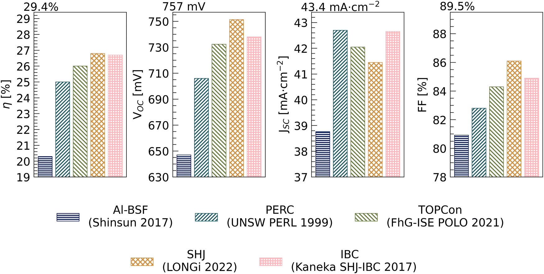 | ||
| Fig. 2 Record current–voltage characteristics achieved with different crystalline silicon solar cell technologies. The values on top of each chart represent the theoretical maximum value of the corresponding parameter based on the Auger parameterization from Niewelt et al.12 | ||
The fundamental difference between the PERC and Al-BSF structure is the dielectric passivation on the rear surface. The main advantage of PERC is that the rear Al-BSF is reduced to small stripes, and this was beneficial because the remaining rear area, not covered by these “local Al-BSFs”, could be effectively passivated by aluminium oxide, AlOx, which came to PV as late as 2004. A schematic illustration of the PERC device structure is shown in Fig. 1. The first report of a high efficiency PERC cell was published by the University of New South Wales (UNSW) in 1989, then using SiO2 (instead of AlOx).34,36 The dielectric layer significantly reduces the amount of recombination centres at the rear surface by passivating dangling bonds.37–39 Additionally, the dielectric can increase the reflection of light on the rear surface, which increases the short circuit current density (JSC). Initial designs incorporated a SiOx/SiNx stack on the rear surface. The SiOx effectively passivates dangling bonds and the SiNx acts as a hydrogen source, however, the intrinsic fixed charge in the SiOx and SiNx is not effective at providing field effect passivation for p-type surfaces. A major advancement was made when the SiOx was replaced with AlOx, which contains a large negative intrinsic charge.40,41 This negative fixed charge repels minority carrier electrons at the p-type surface, further reducing recombination. This field effect passivation has led to surface recombination velocities (SRV) of <2 cm s−1 on p-type silicon,40 which results in very low surface dark saturation current density (J0s) on the rear surface of a PERC cell.42 The term J0s is an important metric used in silicon PV to assess the level of recombination occurring at the surfaces. As such, AlOx has become ubiquitous within PERC cell manufacturing.
Fig. 2 displays a comparison of the record efficiency for Al-BSF and PERC. The efficiency for PERC is increased by about 4%abs. This is primarily related to the VOC, which increases from 647 mV to 708 mV due to improved rear surface passivation. The JSC is also higher due to the improved rear surface reflection. In contrast to the full area contact in Al-BSF, the contacts in PERC are made by forming local openings in the dielectric layer. Compared to the standard Al-BSF cell, the additional processing for PERC is thus the deposition of the dielectric stack on the rear and the laser contact opening. Apart from this, the processing flow is identical to Al-BSF, which made it easily implementable into the existing mass production lines. Due to the vastly improved efficiency with little modification to the process flow, the PERC architecture has completely surpassed Al-BSF as the preferred technology. Fig. 3 displays the market share of silicon cell technologies over time, as taken from the international technology roadmap for photovoltaic (ITRPV) reports. The ITRPV report identifies trends in industrial photovoltaic manufacturing by questionnaires sent to companies and is compiled by a group of international experts associated with various aspects of PV manufacturing, including poly Si producers, cell and module manufacturers and equipment suppliers. Within the silicon community, the ITRPV reports is used as a roadmap to indicate future trends in PV manufacturing. The black line in Fig. 3 represents the estimated market share for the year prior to the report (which closely resembles actual market share), while the coloured lines display the predicted market share from various ITRPV reports.43Fig. 3 displays the more rapid than anticipated decline in Al-BSF in 2019. This directly correlates with a sharp increase in the market share of PERC. This increase in PERC occurred much quicker than previous projections in the ITRPV. Despite the fact that Al-BSF lines could be upgraded to PERC lines, most Al-BSF lines were decommissioned, sometimes over-night. PERC manufacturing required much cleaner factory environments to achieve higher efficiencies. Additionally, lines became more and more automated, and fabrication tools with higher throughput lowered capital expenditure (CAPEX) per GW fabrication capacity enormously. Today, PERC remains the dominant technology, accounting for ∼ 90% of the market share in 2022, despite past predictions in Fig. 3. The main reasons for this dominance are that mass fabrication has reduced technological diversity and complexity to a degree that inter-firm knowledge spillover has increased tremendously.44 On top of this, cell manufacturing is primarily clustered not only in one country but in one region near Shanghai, which improves the mobility of employees and hence the inter-firm transfer of skills. The lower degree of complexity also allows R&D departments to decode and absorb external knowledge more easily.44 Si PV has the lowest number of international patents of all the fields of PV45 and in China, companies file national patents mainly to signal their inventiveness rather than to protect their inventions. For these reasons, improvements penetrate the whole Si PV industry very rapidly, leading to incremental but steady development that formed the fast “moving target” of the PERC technology. This has made it difficult so far for other cell designs, discussed below, to enter the mainstream.
 | ||
| Fig. 3 Market share projections for each silicon technology based on the International Technology Roadmap for Photovoltaics (ITRPV) annual reports. The black lines represent the estimated market share of the year prior to each report, which provide an estimate of the actual market share in each year. Figure based on ref. 71. | ||
The dominance of PERC is related to the combination of much higher efficiency and only slightly increased manufacturing cost compared with Al-BSF. However, the VOC of this approach is still limited. Historically, this was caused by the direct contact between the metal and semiconductor. In regions where the metal directly contacts the silicon, dangling bonds remain unpassivated, so the J0s in these regions (referred to as J0s,met) is much higher than in non-contacted regions. This caused significant recombination in early cell designs. However, in industrial PERC cells, the fraction of metal regions is small (∼2%) and the J0s,met has been drastically reduced due to optimisation of the metal pastes.46,47 Thus, the impact of recombination in contacted regions on VOC potential is diminishing. Instead, the VOC in PERC solar cells is primarily limited by recombination losses in the n+ emitter region. This is due to a rather heavy phosphorus diffusion, causing Auger recombination and surface recombination.48–50
To overcome this recombination, the contacts should be designed such that they provide the dual purpose of passivating the surface and extracting charge, while removing the need for a heavy diffusion in the c-Si. Such a design is referred to as a ‘passivating contact’, this area of research has received immense interest over the past decade with the aim of overcoming the efficiency limitations of PERC cells.51–53 Materials investigated to achieve passivating contacts include thin oxide/doped polysilicon,54 amorphous silicon55 and various metal oxides.56,57 Of these, only the combination of a thin silicon oxide coated with a heavily doped polysilicon layer has been intensely studied as a passivating contact for industrial silicon solar cells.58,59 This passivation approach removes the need for a heavy diffusion in the following way. A tunnelling oxide on the wafer surface only allows one type of charge carrier to pass because there is a highly doped polycrystalline silicon layer behind, which pins the Fermi level to a band, which, in turn, is contacted by metal. Since the blocked charge carrier type cannot reach the metal contact, recombination at the Si/metal interface does not affect cell performance. Additionally, the tunnelling layer can be very well passivated. The heavy doping of the poly-layer only slightly diffuses into the wafer, so this contact can be applied over the whole cell area. Research into this contact approach first appeared in the 1980s,60,61 however, the incorporation into a silicon solar cell re-emerged in 2014.54,62 Such a structure is referred to as a tunnel oxide passivating contact (TOPCon) solar cell.
A schematic illustration of the TOPCon cell architecture is displayed in Fig. 1. Silicon cells adopting this contacting scheme may also be referred to as polysilicon-on-oxide (POLO), since the current transport can occur via pin-holes in the interfacial oxide enabling direct contact between the doped polycrystalline layer and the underlying Si wafer - not exclusively tunnelling – depending on the thickness of the interfacial oxide.39,63–65 TOPCon cells are typically fabricated on an n-type wafer, with the thin oxide and n+ doped polysilicon forming the n-type contact on the rear surface. This contact is also coated with a hydrogen-containing dielectric which releases hydrogen during contact firing and acts as either as a reflector or ARC for bifacial cell structures. The n+ doped TOPCon rear contact serves as an excellent passivating contact, with reported J0s < 3 fA cm−2 and corresponding resistivities <3 mΩ cm2.54,66,67 The surface passivation is controlled by the combination of chemical passivation of defects at the c-Si/SiOx interface, as well as field effect passivation provided by the heavily doped poly silicon layer.
In contrast to PERC, which contains localized rear contacts, the rear surface contact is full area, which has the additional impact of avoiding current crowding on the rear.68 In a TOPCon solar cell, the thickness of the SiOx is carefully controlled to ∼1.3 nm such that tunnelling of carriers can occur. To promote the tunnelling current, the thickness must be precisely controlled. Alternatively, a slightly thicker oxide may be employed and other current transport mechanisms, such as conduction through pinholes, can be utilized.63 This partially reduces the stringent thickness control required to facilitate tunnelling, however, high temperature treatments are required to amplify alternative conduction pathways.64 The efficiency potential for TOPCon cells is higher than PERC. Fig. 2 shows that demonstrated efficiency for TOPCon has reached 26%. This is related to the higher VOC potential of 720 mV for the following reasons. Firstly, the rear passivating contact and the front boron diffusion have both lower J0s values than front and rear of PERC. Secondly, the base doping can be lower than in PERC due to the higher electron than hole mobility, which enables high bulk excess carrier lifetimes. A concomitant increase in FF is observed, related to the higher pseudo FF (pFF) caused by the higher VOC69 and by a relatively higher share of Auger in the recombination processes.70
In mass production, TOPCon cells are typically ∼24.5% efficient, which is about 1%abs more than PERC. However, it is important to note that TOPCon cells – despite becoming mainstream – are limited by the front surface. On the one hand, boron-diffused surfaces have higher recombination losses than phosphorus-diffused surfaces. One the other hand, recombination at the front contact is very high because the boron concentration is lower than phosphorus concentration in PERC, due to lower dopant solubility. These factors will limit the scope for further efficiency enhancements in industrial manufacturing, provided the manufacturing process should remain relatively simple (the 26% efficient cells in Fig. 2 were achieved with elaborate processing). Adding a passivating contact to the front side currently appears to be difficult because even a very thin poly Si layer would cause significant parasitic absorption at the front, so the passivating contact must be restricted to the front finger area, which increases processing complexity.
TOPCon cells are currently becoming mainstream despite manufacturers' lower margins than with PERC. This may be surprising but is driven by two key factors. First, the PV industry is currently expanding by near 50% per annum, so tools are bought in large quantities. Investing such resources into PERC is risky, as the efficiency potential is close to saturation. Second, once TOPCon is dominating the market, PERC lines will probably not be upgradable to TOPCon, even though only two new tools need to be added and most lines have reserved floor space for this. This is expected to be so because the other tools have improved in throughput (up to 10000 wafers per hour) and in quality, so too many tools would have to be upgraded. However, the current introduction of TOPCon cells into mainstream poses risks considering that TOPCon efficiency may be hard to improve further due to limitations at the front surface. This is in sharp contrast to PERC, which has improved by ∼3.5%abs since becoming the dominant commercial technology.
An alternative approach to form a passivating contact is hydrogenated amorphous silicon (a-Si:H).55,72 This can provide excellent chemical passivation at the c-Si/a-Si:H interface, due to the concentration of hydrogen in the film, which passivates dangling bonds, as well as achieving good conduction through the a-Si layers. Passivation with a-Si:H is incorporated into a cell via the silicon heterojunction (SHJ) architecture, a schematic diagram of a typical SHJ solar cell is shown in Fig. 1. The early development of this cell design was driven by Sanyo (acquired by Panasonic in 2009), who championed this approach in the 1990s.73,74 In contrast to Al-BSF, PERC and TOPCon, SHJ cells do not contain a thermal diffusion of dopants into the c-Si to form a p–n junction within the silicon itself (often referred to as a ‘homojunction’). Instead, the carrier selectivity is determined by doping in the a-Si layers. Due to the removal of the thermal diffusion of dopants and firing of metal pastes to form the contacts, the temperature range of SHJ manufacturing is typically <230 °C, which is much lower than PERC and TOPCon. As a consequence, low temperature screen printed silver pastes are used for contact formation. In the initial iteration of the technology, the doped a-Si layers were deposited directly onto the c-Si. However, the defect density in these doped layers is large, thus, the surface passivation was ineffective and devices with this configuration did not achieve high VOC. To overcome this issue, a thin undoped or ‘intrinsic’ layer (a-Si:H(i))) is deposited on the surface to provide excellent surface passivation.75 The large hydrogen concentration in these films facilitates very effective chemical passivation, where the dangling silicon bonds at the surface are saturated with atomic hydrogen. This is characterized by a reduction in the density of interfacial defect states, Dit.75,76 In addition to this effective surface passivation, the lack of heavy doping at the c-Si surface reduces the constraints placed by Auger recombination and thus VOC as high as 750 mV has been achieved with SHJ cell architectures.77,78 In a standard p–n junction, the lateral conduction of carriers occurs in c-Si, either in the emitter or the bulk. However, due to the defect density in the doped a-Si causing relatively low mobility, the lateral conductivity is poor. Therefore, it is necessary to include a transparent conducting oxide (TCO) to allow for lateral conduction of carriers to the contact metal fingers, the TCO is displayed in Fig. 1. The achievable efficiency for the SHJ architecture is better than all purely crystalline Si architectures. As shown in Fig. 2, the record efficiency of 26.8% was achieved with a SHJ structure. These excellent efficiencies are caused by the high VOC (∼750 mV) as well as exceptionally high FF (∼86%). The efficiency values are higher than all other Si technologies and represent a significant increase compared with PERC. However, despite this clear efficiency advantage, SHJ cells have still yet to capture a large share of the market. Fig. 3 displays the forecasted increases in the SHJ market share which have yet to be realized, with the current market share at ∼2%. One of the main barriers to market entry has been the larger capital expenditure for a SHJ production line, compared to PERC and TOPCon, due to both expensive manufacturing tools and expensive safety infrastructure for the gasses. Additionally, the intrinsic a-Si layer cannot be deposited in a PECVD tube, where wafers are stacked in boats, but must be laid side by side. This prevents larger wafers from helping to achieve higher throughput. Investments in SHJ lines were considered risky because the manufacturing tools are incompatible with PERC and TOPCon lines, so downgrading to cheaper cell designs is impossible. However, recently, the situation changed. Because TOPCon cells are limited by the front contact, which is not passivating, and there are no upgrades to TOPCon in immediate sight, this has piqued manufacturing interest in SHJ as the next upgrade. Chinese tool manufacturers took on a simplified engineering approach in tool development and are reducing CAPEX over time. The promise of high efficiency has sparked significant commercial interest, with companies such as LONGi, Tongwei and Hevel Solar producing SHJ and companies such as Meyer Burger and Tri Sun establishing new heterojunction production capacity in Europe. The schematic diagram shown in Fig. 1 depicts the standard industrial approach to SHJ manufacturing. This includes a thin intrinsic layer and doped n+ a-Si layer on the front surface, covered with ITO for lateral conduction. The rear surface contains a stack of intrinsic and p+ doped a-Si, coated with ITO. Over the past couple of years, concerted efforts have been made to improve the cell design. In particular, intense research efforts have aimed to reduce the parasitic absorption losses. The presence of the intrinsic and doped a-Si layers, as well as the ITO, causes severe parasitic absorption on the front surface, which limits the JSC.79 As such, SHJ cells with the standard cell architecture shown in Fig. 1 typically have JSC values limited to approximately 38 mA cm−2. This is much lower than industrial PERC cells, which typically achieve ∼41 mA cm−2 due to the dielectric ARC on the front surface. One approach to reduce such parasitic absorption losses is to replace the n+ doped a-Si on the front with an alternative that has less absorption at short wavelengths. Examples of this include ZnO as an electron selective contact and MoOx as a hole selective contact.80–82 The ITO layer contributes to parasitic losses and is also required on both the front and rear surface. This layer is additionally problematic due to the scarcity of indium, which will severely limit the upscaled manufacturing of SHJ cells (this is discussed at length in Section 5.1). As such, the development of ‘TCO free’ SHJ cell designs are gaining interest.83
The final cell design detailed in Fig. 1 is the interdigitated back contact (IBC) design. The unique aspect of IBC cells is the lack of contacts on the front surface. Both p- and n-type contacts are located on the rear surface in an ‘interdigitated’ arrangement. This means there are no optical losses on the front surface due to the reflection of light from metal contacts. However, the lateral collection of excess carriers at the rear side is limited to ‘electronic shading’. Hence, this architecture offers the potential for high JSC. IBC cells were initially designed for concentrator applications, where the light intensity is much larger than 1 sun.84 For this high light intensity, resistive losses, particularly related to the sheet resistance of the front emitter in other cell architectures, are more problematic. Placing all contacts on the rear, where they can occupy a much larger area, significantly reduces the resistive losses. The p- and n- contacts on the rear can be formed via various passivating contact methods. For example, the previous world record efficiency of 26.7% for a single junction silicon cell was achieved by using an IBC architecture with a-Si passivation, as with the SHJ design. The performance parameters are displayed in Fig. 2. Note the much higher JSC value compared with the standard SHJ cell design. A POLO style approach can also be used, an efficiency of 26.1% was achieved with a POLO IBC architecture.64 Although this contacting scheme provides benefits, it also modifies some of the design requirements. The tolerable surface passivation on the front surface is more stringent for IBC, as all carriers need to be transported to the rear. In the same way, the bulk lifetime of the silicon wafer must be high to allow for sufficient carrier diffusion and collection at the rear. Having contacts with both polarities on the rear increases the complexity and cost of processing, due to the precise patterning required. This increased complexity has limited the commercial uptake of IBC cells. As shown in Fig. 3, the predicted market uptake of IBC cells has vastly outweighed the reality, which closely reflects the projections for SHJ cells. Despite the small market, US manufacturer Sunpower has maintained leadership in the commercial production of IBC cells, demonstrating an efficiency of 25% suitable for area-constrained sectors.
3. Tandem design
3.1. Architecture (two-terminal (2T) vs. four-terminal (4T))
Tandem cells can be fabricated with a variety of architectures. The conceptually simplest design from a manufacturing viewpoint is four-terminal (4T), where two individual cells, made with different Eg, are stacked together. A schematic illustration of a 4T architecture is shown in Fig. 4a. In this arrangement, the cells are optically coupled, meaning that the incident light is shared between the two cells. However, the cells each have their own positive and negative contact and thus are not electrically coupled. Each individual cell will generate an I–V curve that is electrically independent of the other, although the incident light is shared between the cells. Due to the physical separation of the fabrication of each cell, the processing conditions can be optimised independently, which reduces the constraints on cell processing. The fact the cells share the same light source does mean that at least three transparent contacts are required, so that the bottom cell can absorb light. This places a practical limit on the achievable efficiency. Although the processing is less constrained, 4T tandem cells are fundamentally different to a single junction silicon cell, as there are now four contacts. This makes the formation of modules and BOS design more difficult. Due to this difficulty, less research has focused on 4T designs as a viable approach for commercial module manufacturing. | ||
| Fig. 4 Schematics of the different interconnection schemes for tandem solar cells. (a) four terminals, (b) three terminals and (c) two terminals. Please note that for simplicity the same contact order was used (p-type contact on the rear, n-type contact on the front). | ||
An alternative approach, which seems more favourable for module manufacturing, is the two -terminal (2T) approach. A schematic of a 2T design is shown in Fig. 4b, which shows that the cell contains only one positive and one negative contact. In this case, the top cell and bottom cell must be fabricated together to make one combined system, this approach is often referred to as ‘monolithic’. This is much more favourable for module formation and system design, as the contact scheme mimics that of a single junction silicon cell. Additionally, only one transparent contact is required, which can reduce parasitic absorption losses. Furthermore, since the overall current density generated by the tandem cell is approximately half that of the single junction silicon cell, the conductivity of the transparent contact can be reduced by a factor of 4, for the same resistive power losses. However, the fabrication of both cells onto one substrate in a monolithic fashion introduces many new design constraints that are not present in the 4T architecture. First, the processing sequences used, including the temperature, use of solvents and surface preparation, must be compatible between the two individual cells. Second, due to the electrical coupling, the series connection means that the overall photocurrent is limited by the lowest sub-cell current. To maximise efficiency, the current must be matched between the two cells. Therefore, the Eg and thickness of the absorbers, parasitic absorption within non-active layers and internal reflections and interference between layers of varying refractive index must be carefully controlled. The subcell photocurrent limitations imposed by electrical coupling result in a narrower optimum bandgap for the top cell than 4T counterparts.19
To overcome some of these drawbacks of 2T and 4T designs, a three-terminal (3T) configuration is introduced,85 as shown in Fig. 4c. In this configuration, an IBC architecture is utilised for the Si bottom cell. The top cell is grown monolithically, which reduces the need for two TCOs in the top cell, as with the 4T case. This reduces the current loss due to parasitic absorption at the interface layer. This structure also alleviates the need for precise current matching conditions, which is a major design constraint for 2T design. The third terminal allows the additional current from either cell to be extracted.86 This also means that the cell is robust against spectral variations that occur throughout the day at different location on earth. However, for 3T, a complexity arises on the fact that it requires an IBC configuration for the bottom cell. From an industrial point of view, this may be less of a problem now than in the past, since more companies are now producing IBC cells with simpler processing steps. Another aspect of this 3T idea is modifying the 4T configuration to 3T connection. As previously mentioned, from module manufacturing point of view, the additional terminal adds significant cost to the BOS component. If the rear contacts of the two cells are connected, this will result in 3T configuration, while still maintaining the simplicity of the individual cell fabrication process as well as the reduced constraints of current matching.
3.2. Perovskite configuration
Perovskite solar cells originate from the dye-sensitized solar cell community. Perovskite absorbers were first employed to sensitize a mesoporous n-type titania semiconductor to visible light.87 Switching the liquid junction electrolyte to the benchmark hole transport material [2,2′,7,7′-tetrakis(N,N-di-p-methoxyphenyl-amine)9,9′-spirobifluorene] (spiro-OMeTAD) pushed efficiency beyond 10% and eliminated deleterious stability issues arising from the liquid electrolyte.88,89 A key development was the elimination of the mesoporous scaffold,90–92 termed a planar heterojunction device. This innovation opened up the possibility of using planar contacts made with organic n- and p-type materials developed by the organic electronics community. Efficient devices were soon demonstrated on top of p-type layers in an ‘inverted polarity’ architecture.93,94 Inverted polarity refers to a device structure with the p-type contact on the bottom (sun-facing side), rather than the n-type contact on the bottom. To avoid confusion, the community adopted the terminology n–i–p to designate a device where the ‘intrinsic’ perovskite is deposited atop an n-type layer, then coated with a p-type layer (Fig. 5(a)). The p–i–n configuration is used where the perovskite is deposited on the p-type layer before an n-type layer completes the stack (Fig. 5(c)). Thus, the configuration n–i–p or p–i–n designates the sequence of fabrication, regardless of the sun-facing side (Fig. 5(b) and (d), respectively). In a single junction device, where the layers are all processed on a TCO-coated substrate, this configuration also represents the pathway of incident light. However, this is reversed in a 2T tandem with silicon, since the device is completed with a top TCO, rather than built upon one. A detailed review of the early evolutionary development of perovskite architectures is beyond the scope of this manuscript, and the keen reader is directed to the following reviews.95,96 | ||
| Fig. 5 (a) n-i-p perovskite single junction solar cell where the n-type contact faces the sun, (b) n-i-p perovskite/silicon tandem solar cell where the p-type contact faces the sun, (c) p-i-n perovskite single junction solar cell where the p-type contact faces the sun, (d) p-i-n perovskite/silicon tandem solar cell where the n-type contact faces the sun. | ||
The first perovskite/silicon tandem solar cell featured an n–i–p configuration using the benchmark titania and spiro-OMeTAD n- and p- charge transport layers, respectively.97 Since sunlight is incident on the p-type side, contrary to the standard n-type sun facing direction, the optical properties of the HTL become critical. This architecture suffers from parasitic absorption from the HTL that is not experienced in single junction configurations, which limits the conversion efficiency.11,21 Single junction devices with n–i–p configurations have historically had higher efficiencies than their p–i–n counterparts. Due to the reactivity of the perovskite layer, the charge transport layers deposited atop the perovskite are exclusively organic, since they can be deposited by soft means, such as solution processing and thermal evaporation. However, the absence of an organic HTL with good transparency over the entire solar spectrum required to absorb in both sub-cells, motivated the development of p–i–n perovskite solar cells for tandem applications,98 where optically thin layers of the n-type C60 have little parasitic absorption.
Today, p–i–n is the polarity of choice in multiple demonstrations of perovskite/silicon tandem solar cells with conversion efficiencies above 28%, including the previous world record of 31.25% and presumably the present world record of 32.5%. Yet, Aydin et al. have recently demonstrated conversion efficiencies exceeding 27% for an n-i-p perovskite/silicon solar cell, employing a very thin organic p-type layer in combination with a vanadium oxide p-type “buffer layer”.99 In a perovskite/silicon tandem structure, the front perovskite cell produces the larger fraction of the power. Therefore, one should choose the perovskite polarity that favours the perovskite top cell. However, the choice of perovskite polarity, silicon wafer polarity and p–n junction location in the silicon bottom-cell are interconnected. The wafer type determines the junction location for a given perovskite polarity. Similarly, selecting the junction location will determine the silicon wafer polarity required.
In traditional p-type silicon homojunction solar cells, the p–n junction is located at the front. The same was observed in the first n-type SHJ solar cells. However, the high quality of n-type silicon wafers used in SHJ solar cells enabled a shift of the junction to the rear of such devices. Due to continuous improvement in the carrier lifetime of p-type silicon wafers, the same could happen to p-type homojunction silicon solar cells.
Switching to a rear-junction configuration can be advantageous in a single junction silicon solar cell, as the electrical requirements of the front surface layers are relaxed. This provides room for minimising optical and recombination losses in these layers. However, the ideal silicon bottom-cell p–n junction location is not yet defined for perovskite/silicon tandem solar cells.
Recent work from Ballif et al. suggested that a front-junction configuration minimises the negative impact that shunts in the perovskite top-cell have on the conversion efficiency of the complete tandem device100. This was evidenced in their work, where p–i–n perovskite/silicon tandem solar cells were fabricated with p- and n-type FZ silicon wafers featuring poly-Si carrier selective contacts. Combining a p-type silicon wafer with the p–i–n perovskite structure (hence a front junction) resulted in a peak-conversion efficiency of ∼28%. On the other hand, when an n-type silicon wafer was used (hence a rear junction), they observed a peak conversion efficiency of only ∼24%. This example illustrates the importance of considering the relationship between perovskite polarity, silicon wafer polarity and p–n junction location when designing perovskite/silicon tandem solar cells.
3.3. Interconnection schemes in monolithic tandems
As discussed earlier, 2T monolithic tandem cells are composed of two sub-cells, each with a positive and negative side, however, the total device only has one positive and one negative terminal. Therefore, to ensure current continuity across the whole device, one type of carrier from the top cell must recombine with the opposite carrier type from the bottom cell. This occurs at the interface between the two cells. In 2T perovskite/silicon tandem solar cells, three main types of interconnection approaches have been explored. These are displayed schematically in Fig. 6.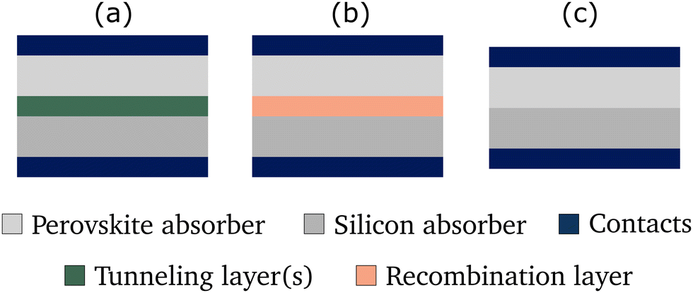 | ||
| Fig. 6 Different tandem interconnection arrangements (a) tunnelling layer, (b) recombination layer, (c) interconnection free. | ||
The first approach is a heavily doped tunnel junction, as displayed in Fig. 6(a). The first demonstration of a tunnelling diode was presented in 1958 by degeneratively doping a germanium p–n junction.101 Quantum mechanical tunnelling refers to the movement of electrons through classically forbidden regions. This is facilitated by heavily doping both the p- and n-side, such that the depletion region width is significantly reduced. In a perovskite/silicon tandem under illumination, a constant supply of electrons and holes will flow to this junction and annihilate via interband tunnelling. For a p–i–n perovskite arrangement, holes are supplied by the perovskite while electrons are supplied by the silicon cell).102 The physical principles of this process in tandems are comprehensively reviewed in ref. 102. This tunnel junction approach was commonly used in III–V tandem structures, which contain degenerative doping and atomically sharp interfaces. Mailoa et al. took this approach in the first demonstrations of a 2T perovskite/silicon tandem solar cells.97 The tunnel junction was formed by depositing a n-doped a-Si layer via PECVD on top of a p++ doped silicon emitter. The a-Si was subsequently annealed at 680 °C for 15 mins to activate the dopants. This device architecture used an n-i-p perovskite arrangement, therefore electrons were injected from the perovskite through the TiO2 electron transport layer towards the interconnection, while holes were injected from the p++ silicon emitter.
Efficient tunnelling in such structures requires an interface between two degenerately doped regions. In some cell architectures, this is not always achievable. In this case, it is possible to enhance recombination of majority carriers by the insertion of a ‘recombination layer’.103,104 This is achieved by the formation of a ‘metallic’ layer in between the silicon and perovskite solar cells, TCOs such as ITO are typically used. This is displayed schematically in Fig. 6b. In essence, the recombination that occurs is similar to Shockley Read Hall recombination in the silicon bulk, however, it involves majority carriers from two different absorbers, rather than a majority and minority carrier within silicon. In principle, this could also be achieved by the inclusion of an ultrathin metal layer. This interconnection approach is particularly suited for SHJ cells, as they already contain a TCO on the front surface, which is already optimised for a low contact resistivity. The main drawback of this approach is the parasitic absorption introduced by the addition of the TCO.97,98 Additionally, the sheet resistance of this added conductor must be carefully considered. If the overlying perovskite top cell suffers from severe shunting due to pinhole formation (for example due to a textured surface), the sheet resistance of the layer must remain high to avoid shunting102. Notably however, since conductivity in the laterial plane is not required, nor desired, very thin (∼10 nm) or low conductivity (∼1000 Ω □−1) TCOs are ideal, and hence additional parasitic absorption losses can be minimised. Using this approach, Zheng et al. recently reported a conversion efficiency of 27.2% (FF = 82.4%) for perovskite/silicon tandem solar cell featuring a 1.7 nm-thick sputtered ITO interconnection layer.105 Interestingly, the authors observed non-complete coverage of the silicon bottom cell surface for thinner sputtered ITO layers.
A third approach is the so-called ‘interlayer-free’ design, in which the top cell and bottom cell are directly connected. This is displayed in Fig. 6c. The advantages of this approach include, (i) possible simplified device processing, (ii) avoiding additional parasitic absorption and (iii) minimising shunting issues by removing the conductive TCO. However, to satisfy the conditions of current continuity, carriers must be able to recombine at the interface. Shen et al. demonstrated an interlayer-free tandem cell approach by depositing n-type TiO2 by ALD on top of underlying p+ silicon.106 This TiO2 layer additionally acted as the n-type layer for an n–i–p perovskite top cell. Low contact resistance was attained at the interface, leading to an efficiency of 24.1% with a passivating contact silicon bottom cell.
4. Silicon bottom cell design
4.1. Silicon wafer type
There are many considerations when choosing the most appropriate silicon wafer type for each cell technology. The first is the crystal structure. The simplest and lowest cost approach to silicon wafer fabrication is directional solidification to form multi-crystalline silicon (mc-Si).107 In this approach, molten silicon in a crucible is solidified to form a brick. As implied by the name, this wafering technique produces silicon wafers that do not contain the same crystal orientation, instead, the material contains small crystal grains of varying size and orientation. This reduces the material quality, due to the amount of structural defects and grain boundaries, which can be electrically active and act as trap sites for metallic impurities.108 Thus, although mc-Si wafers are significantly cheaper to produce, the material quality is low, which limits the efficiency of subsequent solar cells. Nevertheless, until 2017 mc-Si wafers dominated the market. One reason for the initial dominance of mc-Si was the fact that the surface passivation of industrial cells was not well developed, meaning the efficiency was less sensitive to bulk recombination. This allowed for tolerance of lower quality silicon to be used. However, as surface passivation techniques have rapidly improved, the requirements on the bulk quality of the silicon have become more stringent.109 An alternative approach is to use a seed crystal to form a monocrystalline silicon ingot, which is then sliced into wafers. The most popular technique to do so was developed in 1917 by Jan Czochralski and is referred to as Czochralski (Cz) growth.110 In Cz growth, a pure seed crystal with a particular crystal orientation is dipped into molten silicon, held by a metal pulling rod. As the seed is slowly removed and rotated, a cylindrical silicon ingot is formed that has a uniform crystal orientation, matching that of the seed.111,112 This monocrystalline silicon contains significantly fewer structural defects and can thus achieve higher carrier lifetimes. Since 2018, Cz became the dominant wafer type, owing to significant cost reductions in making Cz ingots and wafers. Monocrystalline silicon wafers can also be formed using the ‘float zone’ (FZ) process. In float zone manufacturing, a molten region is made in a Cz silicon ingot by a moving a heating coil along the axis and surrounding a section of the silicon ingot. Impurities and dislocations are preferentially segregated into the molten region, which is moved to the top of the ingot and subsequently removed. In this way, very high purity monocrystalline material, with exceptionally high bulk lifetime, can be formed.113 However, the additional cost of FZ means it is not cost competitive for commercial cell manufacturing.The second consideration is the doping polarity of the wafer. Silicon wafers can either be p-type, by doping with either boron or gallium, or n-type, by doping with phosphorous. Historically, silicon solar cells have been fabricated with p-type wafers. Although p-type wafers displayed poorer electrical properties, they exhibited better tolerance to radiation experienced in space, extra-terrestrial applications as such were the primary applications during the 1960s.114,115 There are several technical factors that also make p-type advantageous for manufacture of industrial cells. First, the segregation coefficient of boron at the silicon liquid–solid interface is much higher than phosphorous.116 This means that the doping concentration of a boron-doped p-type wafers is much more uniform across the ingot than for phosphorous doped n-type, allowing for greater ingot utilisation within the required resistivity range. Second, minority carriers in p-type are electrons, which have a higher mobility than holes by approximately a factor of 3 (depending on the doping level).115 This can relax the requirements for the bulk diffusion length compared to n-type. Additionally, forming an n-type emitter in p-type silicon is less technically challenging than the formation of a boron emitter. As such, using p-type wafers in a PERC architecture allows for more emitter optimisation through the formation of a selective emitter.
From a fundamental viewpoint, the upper practical efficiency limit is similar for p-type and n-type wafers,12 however, in practice, n-type Cz wafers typically exhibit better material properties. The wafer polarity influences subsequent cell processing. For example, PERC cells are typically processed with p-type wafers. Emitter formation therefore requires an n-type region at the surface, which is achieved by a thermal diffusion with a phosphorous source. Instead, in TOPCon cells n-type wafers are typically required, which means that the emitter formation requires a p-type region, formed by a boron diffusion. Thermal diffusion with boron requires higher temperatures and longer times and is thus less desirable for production. The primary reason for the continued dominance of p-type wafers is the cost. In 2021, LONGi stated that the cost of n-type Cz wafers is 10% higher than p-type Cz. The increased cost for n-type is related to increased brick costs, due to the fewer times the crucible can be re-used, lower yields and stricter impurity requirements.117
Another critical wafer property is the bulk lifetime. This determines how well carriers generated in the bulk can be transported to the contacts for collection and thus has a large impact on the cell performance. The bulk lifetime provides a measure of the amount of recombination-active defects in the silicon wafer. Crystallographic defects can cause recombination in the bulk, thus, mc-Si wafers typically have lower lifetimes, which limits cell efficiency. Although Cz wafers have significantly less crystallographic defects, impurities in the bulk can also cause undesirable recombination. Thus, Cz wafers can have bulk lifetimes spanning several orders of magnitude, depending on the concentration of contaminants. The unintentional incorporation of oxygen during ingot formation can lead to the formation of boron–oxygen (BO) defects in boron-doped p-type wafers. The formation of BO defects under illumination has caused significant loss in VOC and efficiency for p-type solar cells.118–120 This can be overcome by replacing boron with gallium as the p-type dopant.121–123 Additionally, unwanted oxygen in the wafer can form oxygen precipitates or thermal donors when processed at elevated temperatures.111,124 These defects appear as circular rings and can manifest in both p-type and n-type wafers.125 Metallic impurities, such as iron, copper, chromium and aluminium can also be incorporated into the wafer during manufacturing.108 These impurities can cause undesirable recombination and can also form recombination-active complexes, such as Fe–B pairs. Thus, there are many factors that can influence bulk recombination and cause reductions in the bulk lifetime. When considering the bottom silicon cell in a tandem structure, it is important to acknowledge that the processing route employed for the silicon cell can modify bulk lifetime. For high temperature processing routes, such as PERC and TOPCon, several processes inherent in the processing can cause the bulk quality to improve. Defect engineering can occur via two processes, (i) high temperature diffusions can migrate impurities to the surface region, which is subsequently etched off. This process is referred to as ‘gettering’. (ii) High temperature firing of hydrogen-containing dielectrics introduces hydrogen into the bulk, where it can passivate defects.126 For SHJ cells, where processing occurs at <250 °C, these defect engineering processes are not incorporated into the cell processing, therefore, this cell architecture has stricter requirements on the wafer quality.109 High temperature processing can also activate grown-in defects, such as thermal donors, which can reduce bulk lifetime. Therefore, it is important to consider not only the bulk lifetime of the as-cut wafer, but also the potential changes in the bulk during cell processing.
Fig. 7 displays a breakdown of the different wafer types used to date for perovskite/silicon tandem solar cells. This demonstrates an overwhelming tendency to use expensive, high lifetime n-type FZ wafers. These are often used for high efficiency passivating contact designs such as SHJ, which is useful to explore the efficiency potential for a specific cell design. However, it must be acknowledged that this wafer type is too expensive for industrial production. It is important to understand the impact the reduce bulk quality of Cz wafers will have on the practical efficiency of industrial perovskite/silicon tandems.
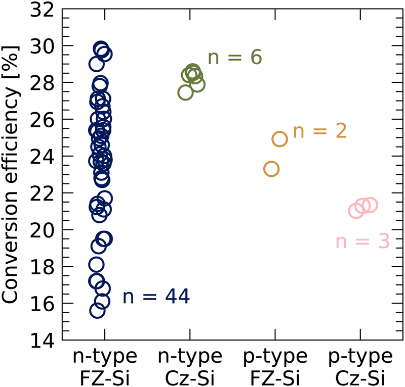 | ||
| Fig. 7 Comparison of reported cell efficiencies for different wafer types used for perovskite/silicon tandems. Note, the world record efficiencies are not shown due to lack of reported information. | ||
4.2. Silicon surface optics
A bare silicon wafer in air has reflectance in the range of 30–40%. In a single junction silicon cell, there are two main processes used to reduce the reflection on the front surface. The first process is texturing, which refers to a chemical etching process to change the physical structure of the surface. In monocrystalline wafers, the different etching rates for different crystallographic planes is exploited. An alkaline chemical etchant, typically potassium hydroxide (KOH), is used to anisotropically etch the surface. The etching rate of the 〈100〉 plane is much faster than for the 〈111〉 plane, therefore, careful control over the solution concentration and etching temperature can preferentially etch the 〈100〉 plane, leaving the 〈111〉 planes exposed. This leads to the formation of a pyramidal structure on the front surface. Fig. 8a shows an SEM image of a typical industrial textured silicon surface. The size of the pyramid base is typically in the range from 3–8 μm. On a planar surface, any reflected light is lost and cannot contribute to photocurrent generation. However, when the surface is fully covered with pyramids, the angle of reflection predominantly leads to the reflected light bouncing on a Si surface a second time and being absorbed. Thus, the improved absorption for a textured surface of a bare silicon wafer in air reduces reflection to about 10%. For multicrystalline silicon, which is comprised of many different grains with varied orientations, the same approach cannot be used. Instead, an acidic texturing is used to roughen the surface.127,128 The second approach to reduce reflection is the deposition of a dielectric anti-reflection coating. By carefully controlling the stoichiometry and thickness of the dielectric, typically PECVD SiNx, the reflection is reduced by destructive interference. A typical SiNx layer used as an ARC in PERC solar cells will have a refractive index of ∼2 and thickness of 75 nm. Combining the surface texturing with the ARC can lead to reflectance of almost less than 1% at the optimised wavelength.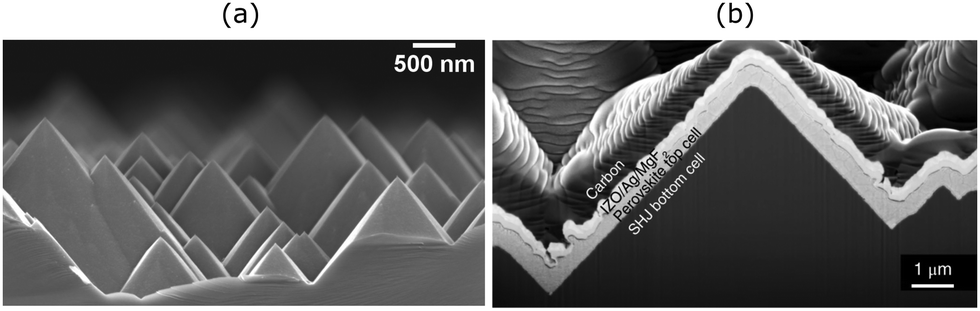 | ||
| Fig. 8 (a) Alkaline textured random pyramids on a monocrystalline silicon surface (b) cross sectional SEM image of the full perovskite solar deposited on a textured silicon surface.129 | ||
Micron-size pyramids are very effective for reducing reflection in single junction silicon solar cells, however, in monolithic perovskite/silicon tandems, this surface is not as compatible with all processing methods used for the perovskite top cells. Due to the small diffusion length in the perovskite material, the thickness must be kept to ≤1 μm to avoid recombination losses. In single junction perovskite solar cells, the layers are commonly deposited via solution processing. However, such thin layers cannot be deposited on top of micron-scale pyramids using solution coating techniques. As such, all demonstrations of monolithic perovskite/silicon tandem cells prior to 2018 were formed using a silicon wafer with a polished front surface. This is advantageous, as the perovskite and carrier selective layers can be deposited conformally, however, the planar surface has three major drawbacks, (i) significantly higher reflection on the front silicon surface, (ii) reduced light trapping at long wavelengths and (iii) significantly increased cost compared with alkaline textured surfaces. In 2018, Sahli et al. demonstrated the first perovskite/silicon tandem fabricated with a fully textured monocrystalline silicon front surface.129 The key to achieving this was the modified perovskite deposition technique. Rather than simply spin-coating, the perovskite layer was formed by a two-step process. The first process involved the co-evaporation of a conformal porous lead iodide (PbI2) and cesium bromide (CsBr) precursor film. Next, the organic ammonium halide salt solution was spin-coated to form the perovskite. The initial co-evaporation process serves as a conformal scaffold for the perovskite formation. The subsequent spin-coating wets and coats the PbI2/CsBr scaffold. The scaffold acts as an anchor, so that the perovskite layer remains conformally coated. An SEM image of the conformal deposition onto the micro-size textured c-Si surface is shown in Fig. 8b. Initial attempts to form the perovskite by spin-coating without the scaffold did not work, the liquid solution accumulated in the valleys of the c-Si pyramids, leading to a non-conformal coating and significant device shunting. The authors achieved an efficiency of 25.2% using the two-step perovskite deposition on a textured surface, which was the highest efficiency for a monolithic 2T device at the time of publication in 2018.129 This significant achievement was attributed to the improved optical management in the textured monolithic device. The fully textured device was compared to a similar device prepared on a polished surface. The loss in JSC in the device with the polished surface was 3.14 mA cm−2. This was reduced to 1.64 mA cm−2 for the textured wafer. The improved photocurrent generation was caused by reduced reflectance on the silicon front surface as well as better light trapping in the infra-red region. Despite the gains in JSC, the efficiency is limited by the relatively low FF of 73.1%.
An alternative approach to improve the compatibility between the silicon surface and the perovskite deposition is to reduce the size of the surface pyramids. Although the industry standard micron size pyramids are not compatible with solution processed perovskite films, reducing the feature size could allow for subsequent conformal solution processing. Alasfour et al. provided a comprehensive study of the use of wet chemical etching to form nanoscale texturing on a silicon surface.130 They showed that the ability to form nanoscale pyramids required both a slow etching rate as well as a large number of nucleation sites. If the ratio of nucleation sites to etch rate is sufficiently large, the surface becomes saturated with nucleation sites so that pyramids of >1 μm dimension are unable to form. To achieve these conditions, Alasfour et al. reduced the etchant concentration to reduce the etch rate and increased the concentration of the potassium silicate (K2SiO3), which controls the number of nucleation sites. By doing so, they were able to create nanoscale pyramids with a wide range of sizes, the minimum pyramid size was 62 nm. Reducing the pyramid size introduces a fundamental trade-off. Smaller pyramids are much more amenable with subsequent top cell solution processing, however, the reduced pyramid size also leads to increased reflection relative to standard micron-size pyramids.130
As an alternative to processing on highly textured silicon, inserting an “optical-interlayer” between the silicon and perovskite top cells can have a similar effect upon reducing reflectance losses. Including the top TCO and anti-reflective coating, the perovskite top cell is composed of up to 7 layers. This is hence an optical stack of materials for which the thickness of each layer requires optimising for minimising reflection losses and maximising absorption in the perovskite absorber layer and forward transmission into the Si cell. A key challenge in minimising the reflectance between the perovskite and silicon layers, is the significant contrast in refractive index of the perovskite (∼2 to 2.5) and silicon (∼3.5). Inserting an optically transparent layer which is approximately the mean of the refractive index of adjacent layers, and with a thickness of ∼ ¼ the wavelength of the relevant light, leads to constructive interference for forward transmission. Mazzarella et al. demonstrated that the insertion of a nanocrystalline silicon/silicon oxide interlayer on top of a mechanically polished SHJ cell resulted in significantly enhanced IR transmission of light,131 and matched the at the time certified world record efficiency of Sahli et al.129
Recent excellent results from EPFL/CSEM and HZB demonstrated monolithic perovskite/silicon tandem cells with efficiency exceeding 30% for both planar and textured wafers. For the planar wafers, the perovskite was fully solution processed, while on the textured surface the two-step “hybrid” deposition process, first described by Sahli et al.,129 was employed. From the CSEM/EPFL work, the efficiency achieved for planar and textured wafers was 30.93% and 31.25%, respectively.100 The slightly higher efficiency on the textured surface was attributed to an increase in JSC of ∼0.6 mA cm−2. As discussed above, this was related to reduced reflection at short wavelengths and improved light trapping at long wavelengths. However, the issue for the textured approach is the lower FF, which was >1%abs lower in the planar cell. If this issue can be addressed by preventing shunting, the efficiency potential for textured wafers could be much higher. However, the increased complexity of the two-step deposition process may introduce a trade-off between cost and efficiency. Notably, the present world-record of 32.5% from HZB was achieved on a polished Si wafer with the inclusion of the nanocrystalline SiOx optical interlayer, regaining the lost photocurrent and sustaining a high FF. This questions whether reduced texture with optical interlayer optimisation is preferable to industrially standard full texture.
4.3. Surface passivation and junction formation approaches
The next choice to make for the bottom cell is the cell architecture. Section 2 provided a comprehensive overview of the existing cell designs for single junction silicon cells. Although PERC cells currently dominate the silicon PV market, by far the most prominent cell architecture for perovskite/silicon tandems with efficiency exceeding 25% is SHJ.132Fig. 9 displays a breakdown of the bottom cell type used to fabricate perovskite/silicon tandems to date. This indicates that SHJ is the most popular choice. There is a range of reasons why the SHJ architecture is advantageous as the bottom cell in a tandem design. These include. | ||
| Fig. 9 Comparison of reported cell efficiencies for different bottom cell architecture from literature. Note, the world record efficiencies are not shown due to lack of reported information. | ||
• Potential for high VOC due to the excellent a-Si surface passivation.
• The cell design already incorporates a TCO on the front surface, which easily integrates into tandems.
• Excellent flexibility of the placement of the n or p selective contact means it can be integrated with different perovskite configurations.
• The parasitic absorption losses at short wavelengths caused by passivation layers and TCO, which are the primary efficiency barrier for single junction cells, are not a problem when used as a bottom cell as short wavelengths are absorbed in the top cell.
Al-Ashouri et al. reported a certified efficiency exceeding 29% for a monolithic tandem device using an SHJ cell as the bottom cell.133 The silicon surfaces are passivated using intrinsic amorphous silicon. The carrier selective layer on the front surface is an n-type nanocrystalline – SiOx, capped with ITO to form the recombination layer. The VOC from this bottom cell was ∼715 mV, under approximately half sun illumination. The certified efficiency and VOC value were 29.15% and 1.90 V, respectively. The same group has further reported improved conversion efficiency for this structure to 29.8%.134 This was achieved mainly by modifying the silicon heterojunction bottom cell structure. First, a sinusoidal nano-texture was applied to the wafer's front surface, which reduced reflection losses and improved fabrication yield in comparison to planar front surfaces. Secondly, the authors implemented a reflector with a dielectric buffer layer, which reduced parasitic absorption at near-infrared wavelengths.
This shows clear potential for high efficiency devices, however, as shown in Fig. 3, the current market share for single junction SHJ cells is <5%. This is caused primarily by the additional costs compared to PERC and TOPCon. For perovskite/silicon tandem solar cells to reach commercial production and thus have a tangible impact on reducing CO2 emissions, a large set of stringent criteria must be met, including efficiency, cost, stability and sustainable production. In terms of manufacturing cost, it is also important to consider other cell designs. Messmer et al. provided a comprehensive analysis of performance, cost and LCOE for tandem cells using four different bottom cell designs.135 Those designs included (i) PERC (which was denoted as P[E]RC as the diffused n+ emitter on the front surface was directly contacted with ITO and thus not technically passivated), (ii) TOPerc, where the n+ diffused emitter was replaced with a tunnel oxide/n+ doped poly Si contact, (iii) TOPCon2, where both surfaces contain thin oxide/doped poly Si (n+ on the front surface), and (iv) SHJ, which followed the standard structure with an n-type wafer, as displayed in Fig. 1. The authors used Sentaurus TCAD for optical simulations of the whole perovskite/silicon stack and Quokka3 for electrical simulations of the silicon cell. Electrical simulation on the perovskite cell were not performed, typical empirical values for performance were taken from literature. Their analysis showed that the highest efficiency potential was achieved with the SHJ bottom cell, the efficiency was ∼1.5%abs higher compared to the P[E]RC bottom cell. The efficiency potential for TOPerc and TOPCon2 was in between SHJ and P[E]RC. The matched JSC for all four bottom cell designs was similar, so the efficiency potential was primarily determined by differences in VOC and FF. The VOC for the SHJ bottom cell was 725 mV, which is more than 50 mV higher than P[E]RC. This was simply attributed to the much better surface passivation from the a-Si layers. Note that this value is lower than typically reported values, as the illumination intensity is lower than 1 sun due to absorption in the perovskite. The FF potential was also highest for the SHJ cell and followed a similar trend to VOC. This was attributed to the higher pseudo FF (pFF) linked to higher VOC. Interestingly, Fu et al. plotted the FF as a function of VOC for sixty-four real I–V measurements of perovskite/silicon tandems.132 A direct correlation between FF and VOC was not observed. In fact, FF was often higher in high temperature homojunction c-Si bottom cell designs that exhibited lower VOC. This indicates that FF losses in real devices are largely governed by resistive losses, indicating significant scope for further efficiency increases. However, we also note that the FF is a minimum when current matching is perfect. Since many experimental cells will not be perfectly current matched, the FF are usually higher than expected from the single junction cells and more variable.
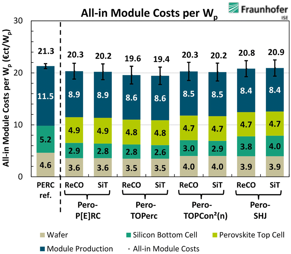
When comparing the bottom cell design in terms of cost of production, a very different story emerged. Of the four cell designs, the cost of TOPerc was the lowest, at 47.8 €ct per cell. This was followed by P[E]RC at 48.4 €ct per cell, TOPCon2 at 54.5 €ct per cell and SHJ at 61.2 €ct per cell. The same trend emerged but with slightly different costs when the recombination layer was replaced with a silicon tunnel junction interconnection layer. Finally, the costs and efficiency potential were compiled to calculate the €ct per Wp for each approach. Fig. 10 displays all module costs, in terms of €ct per Wp, for the four potential tandem configurations, as well as a reference PERC cell. For all cases, the tandem cells have lower cost compared to the PERC reference, however, there is very little distinction in €ct per Wp for the four different bottom cell arrangements. The cost varies from 19.4 €ct per Wp for the TOPerc bottom cell to 20.9 €ct per Wp for the SHJ bottom cell, however, due to the large uncertainty in some cost inputs, the values are all within the stated errors. This indicates that the race for the most appropriate bottom cell is still well and truly on, despite the overwhelming weight of research focus on SHJ cells.
 | ||
| Fig. 10 All-in module costs per Wp for the four investigated bottom cell designs. ‘ReCO’ refers to recombination layer interconnection, while ‘SiT’ refers to a silicon tunnel junction interconnection.135 | ||
One drawback of Messmer et al. analysis is the lack of consideration for sustainability of materials used in each design. For example, the SHJ cell in the above analysis is assumed to contain a 70 nm ITO layer on the rear of the cell, which is not amenable with TW-scale PV production (this is discussed in Section 5.1). As such, it is very useful to consider the industry mainstay PERC design, as it does not require indium and uses less Ag than SHJ and TOPCon.136 Messmer et al. simulated the performance of perovskite/silicon tandems with a range of modified PERC cell as the bottom cell.137 The authors emphasise that quite different design constraints apply when considering the front surface. In terms of a single junction PERC cell, the emitter is designed with the following considerations in mind, (i) the optical properties of short wavelength light, (ii) lateral transport of carriers to metal contacts, (iii) surface passivation, and (iv) low contact resistance with metal contacts. However, in a tandem architecture, the following differences apply, (i) short wavelengths are absorbed in the top cell and are thus not absorbed in the bottom cell, (ii) the magnitude of current is about half, (iii) the cell may not require lateral conduction in the emitter to local points and (iv) there is no thermal treatment for front contact formation. The relaxation of these strict design requirements for PERC may allow for a narrowing of the efficiency gap compared with SHJ, which is currently seen in single junction cells. In their simulations, Messmer et al. investigated five different front surface PERC designs, starting with a heavy n+ emitter in direct contact with the ITO recombination layer, dielectric surface passivation with local openings and a variety of full area front surface passivation schemes. The simplest design, with the P[E]RC front cell yielded and efficiency of 29.5%, which increased to 30.5% for the TOPerc front cell. This efficiency is only 0.7%abs lower compared with a SHJ bottom cell, indicating the potential gains that PERC cells can gain by being incorporated into a tandem cell.
4.4. Metallisation
The contrast in typical processing routes for perovskite and silicon cells is perhaps most acutely felt when searching for metallisation approaches compatible with both cells. Record perovskite single junction efficiencies are typically recorded on very small area devices <1 cm2. Metal contacts in the small devices are formed using thermal evaporation. In this process, the samples are placed in a vacuum chamber under high vacuum (<10−6 torr or mbar). The metal to be evaporated is heated in either a small boat or wrapped around a wire to the point where it vaporizes. The desired contact shape is defined with a simple shadow mask. This method is not currently employed for industrial silicon solar cells, as (i) the deposition rate is typically only on the order of a few angstroms per second, (ii) most of the evaporated metal is wasted coating either the shadow mask or the inside of the chamber and (iii) the deposited metal is orders of magnitude thinner than screen printed contacts, so the line resistance is very high and (iv) the vacuum level required is 103–104 times higher than is required for sputtering. In small area depositions, it is common for the metal contacts to be deposited outside the active cell area, a TCO is relied upon for lateral conduction of carrier to the contacts. This boosts the efficiency as it removes shading losses, however, when large area devices are formed, series resistance losses rise rapidly when using a TCO alone for lateral conduction. Therefore, a full metal contact grid is required. In contrast to very small area perovskite cells, metal contacts in silicon solar cells are formed using screen printing of metal pastes, typically silver or aluminium. The development of screen-printing metal contacts in 1975 revolutionised industrial solar cell design and allowed for the rapid upscaling that has subsequently occurred. Screen printed metal contacts allow for high throughput processing with low enough contact resistance and line resistivity to allow for high FF, even on device areas >200 cm2. LONGi solar announced an efficiency of 26.5% for a full area front and back contacted SHJ solar cell with silver screen printed contacts and Sundrive have achieved >26% on SHJ cells with copper plating. Fig. 11 displays a comparison of solar cell area with the nominal power output for a range of perovskite/silicon tandems, industrial silicon cells and silicon modules. This analysis shows that the area and power output of typical high efficiency perovskite/silicon tandems are orders of magnitudes lower than the current industrial silicon solar cells and modules. For perovskite/silicon tandems to become a serious commercial product, they must traverse this curve to larger areas, with cell areas >244 cm2. To do this, a fundamental shift in the metallisation is needed. | ||
| Fig. 11 (a) Comparison of nominal power and device area for various perovskite/silicon tandem solar cells, industrial silicon solar cells and silicon modules. Figure design based on ref. 139. | ||
Kamino et al. took a first step in this direction in forming a perovskite/silicon tandem by low temperature screen printing.138 They achieved an efficiency of 22.6% on this device, compared with 24.0% for a device with evaporated Ag contacts (area of 1.43 cm2). The screen-printed contacts were cured at 130 °C due to the temperature constraints of the perovskite layer. A substantial loss in FF was observed in the screen-printed cell, primarily due to the contact resistance between the Ag and ITO. In the screen-printed contact cured at 130 °C, the contact resistance was 60 mΩ cm2, as opposed to 0.02 mΩ cm2 for the evaporated Ag contact annealed under the same conditions. The purpose of the curing step is to make the printed contact more compact, which reduces the resistance. When the curing temperature was increased from 130 °C to 210 °C, which is typical of cell processing for SHJ cells, the contact resistance reduced from 60 mΩ cm2 to 10 mΩ cm2. However, curing at this temperature will lead to degradation of the perovskite cell. This tension must be resolved to achieve high quality metal contacting for large area devices. The JSC was also reduced compared to the evaporated cell due to shading from the contacts.
4.5. Summary of design considerations for silicon-based tandems
The design approach for the bottom cell in a 2T tandem is quite different to that of a single junction silicon cell. Here, we summarise the fundamental differences. A graphical overview of some of the critical design considerations is shown in Fig. 12.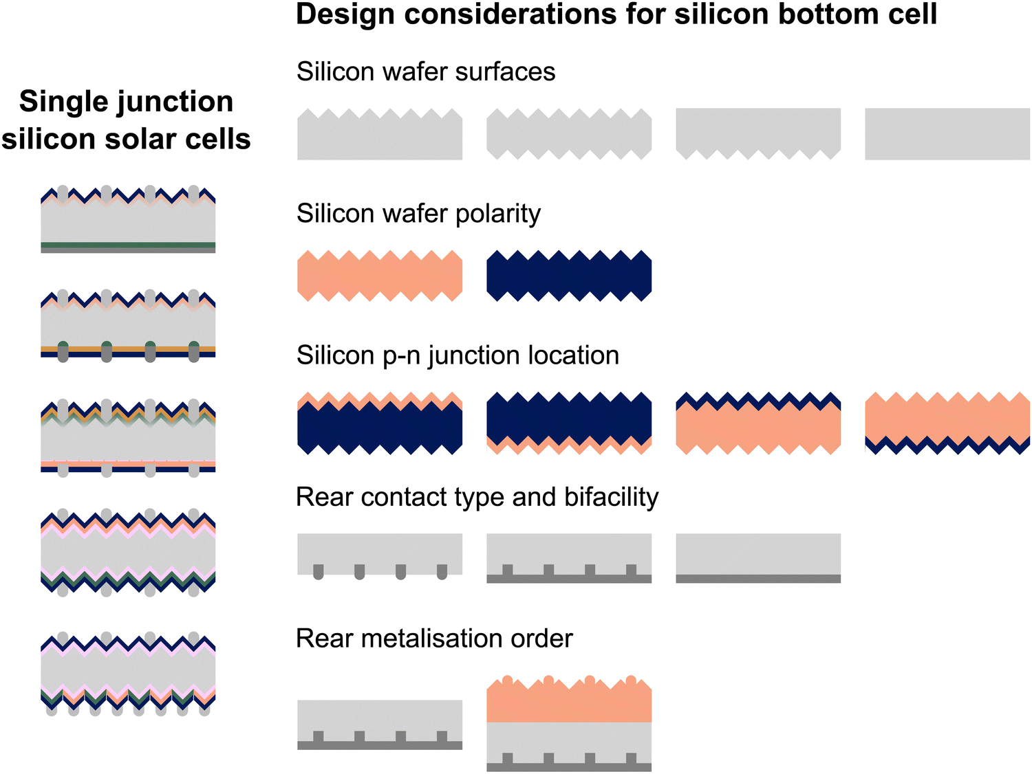 | ||
| Fig. 12 Graphical overview of the design considerations for silicon bottom cell in the tandem architecture. | ||
5. Other design aspects
5.1. Sustainability of materials
To mitigate the impacts of climate change, other sectors besides electricity generation will need to shift away from fossil fuels to renewable energy. The energy transition to 100% renewables requires a drastic increase in the annual production capacity of solar PV. Verlinden and Haegel et al. predicts that a cumulative solar PV capacity of 70 TW is needed by 2050.6,7 This will require a 30-fold growth in the annual production capacity, relative to 2020. Verlinden also warns that to reach this level, rapid initial growth, such that a production capacity of 3 TW is achieved by 2032, is needed to avoid subsequent market instabilities.7 This points to the idea that the next ten years of solar production are critical in fighting climate change.In light of the rapid upscaling of PV manufacturing required over the next decade, the consumption of the materials that go into making solar cells must be closely scrutinised. Most of the body of literature in solar cell research has focussed first on increasing the efficiency and stability of solar cells, then implementing these designs into mass production. Sustainability of the materials used in the cell design must now come to the forefront of the solar community's collective mindset. In particular, silver (Ag) and indium (In) are scarce materials that are integral components of modern solar cell design. Zhang et al. analysed how material consumption demands could limit the expansion of different single junction cell technologies.136 Assuming the PV industry could use 20% of the global supply of a particular material, they estimated that the annual manufacturing capacity was 377 GW for PERC (limited by silver), 227 GW for TOPCon (limited by silver) and 37 GW for SHJ (limited by indium). This alarmingly shows that current cell designs, without modification, are not capable of sustaining a future TW solar PV market. Silver is used for contact formation in all three cell designs. Zhang et al. calculated that the Ag consumption for each cell technology is currently 15.4 mg W−1 for PERC, 25.6 mg W−1 for TOPCon and 33.9 mg W−1 for SHJ.136 PERC has a lower Ag consumption as it uses aluminium for the rear metallisation. By contrast, SHJ structures require Ag metallisation on both surfaces and use more Ag due to the low temperature curing demanded of the a-Si passivation layers. The authors argue that this consumption must be reduced drastically to 2 mg W−1 if TW-scale markets are to be sustained, which has drastic implications for cell design.
As well as material consumption issues, the price volatility of Ag may also become a problem as the PV manufacturing expands. The cost of silver is approximately 10% of the selling price for a solar cell, however, for a smart phone it is only 0.01–0.05%, meaning other competing industries will be much more tolerant to price fluctuations.136
The absolute power loss due to the resistance in metal fingers can be calculated by:

where x is the distance from the middle of the finger to the busbar, JMP is the current density at maximum powerpoint, Sf is the finger spacing, ρm is the line resistivity of the fingers, Wf is the width of the finger, tf is the finger height and SBB is the busbar spacing.

This can be converted to a relative loss in the following way:
Consumption of indium is also challenging for solar cell manufacturing. Although indium is more abundant in the earth's crust than silver, the useable fraction is much lower.136 This is because indium is produced exclusively as a by-product of the processing of other metal-ores, namely zinc.140 PERC and TOPCon cells do not require indium, however indium tin oxide (ITO) is used in SHJ cells to provide lateral conduction to the contacts and serves as an anti-reflection coating. In PERC and TOPCon cell designs, the lateral conduction of carriers occurs in the diffused emitter or silicon bulk. In a standard industrial SHJ cell, the ITO layer on the front and rear surface is typically in the range of 70–100 nm. Zhang et al. performed an analysis of the possible annual production capacity of SHJ cells based on indium consumption. Fig. 13 displays a contour plot showing the annual production as a function of indium usage, in mg W−1, and % use of 2019 indium supplies. The upper and lower limit on indium consumption for industrial SHJ cells was 10.74 mg W−1 and 4.23 mg W−1, respectively, based on literature and discussions with SHJ manufacturers. These upper and lower bounds of indium consumption are shown in the shaded region. Isolating the case where 20% of the total indium is required, this corresponds to an annual production capacity between 35–95 GW. This severe limitation caused by the dependence on ITO means the annual production capacity of SHJ cells, with the current industrial cell design, is more than an order of magnitude lower than required for TW-scale PV. As such, the authors state, “Indium cannot be used in any significant manufacturing capacity for PV production, even for futuristic 30%-efficient tandem devices”.136
 | ||
| Fig. 13 Calculated allowable annual production capacity for SHJ solar cells as a function of both the indium consumption (mg W−1) per cell and % of 2019 global indium supply.136 | ||
Lennon et al. recently raised an additional concern regarding the sustainable production of TW scale solar PV.141 By considering the ITRPV broad electrification scenario, which predicts a cumulative installation of 60 TW of solar PV by 2050, they calculated the required aluminium demand for PV production. The rapid increase in solar PV production demanded of this scenario meant the Al requirement by 2050 would be as high as 28.5 Mt per year. This demand is more than 40% of the 2019 total global Al production. Due to the very high average emissions intensity of primary aluminium production, this would lead to an alarming global warming potential. It should be noted, however, that the contribution associated with cell metallisation was negligible, meaning this would not limit the use of Al for cell designs. The primary contributors to Al demand were module frames, mountings and inverters. These results highlight the need to consider not only the material consumption for the TW scaling of PV, but also the CO2 emissions associated with producing these materials.
5.2. Stability
The final consideration is the long-term stability of the cells and modules. It is widely known that perovskite solar cells have suffered from stability issues, however, significant research and development efforts have been expended upon understanding and mitigating the instabilities. The intrinsic stability issues of the perovskite material, particularly in the presence of moisture, and the various mitigation strategies have been reviewed in the following ref. 142–144. Herein, we focus on experimental demonstrations of stability in tandem solar cells. For a detailed analysis of stability issues in perovskite/silicon tandems, the reader is directed to ref. 145.Liu et al. investigated the performance of encapsulated perovskite/silicon solar cells under outdoor testing conditions in a hot and sunny environment.146 The wide band gap perovskites used to form tandem cells typically show reduced stability compared to perovskites with Eg of 1.50–1.60 eV. These instabilities are often attributed to phase segregation under illumination. In their report, Liu et al. investigated the impact of carbazole as an additive to the perovskite precursor solution to assess the impact on the stability of perovskite/silicon tandems. Before testing, the devices were encapsulated between two pieces of cover glass with black butyl rubber sealant. Outdoor testing was performed on an open rack system at King Abdullah University of Science and Technology (KAUST). The average temperature was 45 °C, which increased to a maximum of 60 °C. The maximum illumination intensity was ∼0.95 suns, measured by a pyranometer. Outdoor testing is rigorous, since it exposes the samples to operation under diurnal illumination, elevated temperatures and heat cycles from night-to-day. Fig. 14a displays the light intensity, power output, VOC, ISC and FF of perovskite/silicon tandems, with and without carbazole treatment across 43 days of continuous testing. At the end of the test period, the control device that was not treated with carbazole exhibited a power output 77% of the initial value. This degradation was seen primarily in VOC, which was attributed to degradation of the perovskite itself. The PCE retention in the carbazole-treated samples was 93% for the 43 days of outdoor testing. First, compared with industrial silicon solar cells, this degradation is large. PV manufacturers routinely providing 25 year warranties on their products, with a typical expected degradation rate of 0.5%/per year. Second, the significant impact that the carbazole treatment had on stability indicates that degradation in the perovskite is limiting the overall stability. Following this, the further indoor testing was performed under continuous xenon lamp illumination with MPP tracking. Fig. 14b displays the power output of the cell under constant illumination for 250 hours. The untreated cell underwent ∼8% degradation. In contrast, the carbazole treated cell did not display any signs of degradation in this testing period. Finally, the cells were tested under damp heat conditions of 85% RH at 85 °C. The results of the damp heat test are shown in Fig. 14c. After 500 hours under these conditions, the cells retained 87% of the initial efficiency. This degradation was caused by losses in FF, attributed to degradation of the top contact.
 | ||
| Fig. 14 Outdoor testing results over 43 days for perovskite/silicon tandem cell. (a) Light intensity, power output, VOC, ISC and FF, (b) power output of cells under constant illumination for 250 hours, (c) damp heat testing at 85 °C at 85% RH.146 | ||
Current matching is very important for maximising the efficiency of a 2T tandem solar cell. Under STC conditions (25 °C), the optimum Eg of the perovskite, when coupled with silicon is ∼1.73 eV.19 When designing to maximise energy yield in a monofacial tandem, this drops to 1.65 eV, and even further when maximising the energy yield in a bi-facial tandem.147 These band gaps are achieved in perovskites by varying the stoichiometry of the halide. However, wider gap perovskites are known to experience phase segregation under illumination, which can cause current and voltage losses.148 Aydin et al. studied the impact of temperature on the performance of perovskite/silicon tandems.149 By varying the temperature from 25 °C to 75 °C, they showed that the current matching in the tandem device changes for varied temperature. This is related to the temperature dependence on the Eg. It is well known that the Eg of c-Si narrows as the temperature is increased. By varying the bromide concentration in FACsMAPbI3-xBrx from 6% to 30%, the Eg of the perovskite at 25 °C was varied from 1.61 eV to 1.73 eV, respectively. The Eg was then measured for four different compositions as a function of temperature between 25 °C and 75 °C. This showed that the Eg of the perovskite widens as temperature increases, which is the opposite trend to the c-Si bottom cells. This implies that the optimum perovskite Eg for current matching at STC conditions may not perform the best under realistic conditions at elevated temperatures. The authors then recalculated the radiative efficiency limits for perovskite/silicon tandems by incorporating the impact of temperature on the Eg. The optimum perovskite Eg, as a function of operating temperature, is shown in Fig. 15. This shows that the optimum Eg shifts to lower values for higher temperatures, which may prompt a rethinking of the cell design. Combining the temperature dependence of the band gap, with the need to maximise energy yield rather than AM1.5 efficiency, and the general trend in the industry towards bi-facial modules, it is likely that the optimised band gap for a perovskite top cell is closer to 1.5 eV than to 1.7 eV.150 This has a practical benefit for mixed bromine-iodine halide perovskites, as bromide-lean compositions, with Eg < 1.65 eV, are more stable under illumination due to less halide phase segregation and are also easier to obtain comparatively higher efficiency.148,151
 | ||
| Fig. 15 Calculated optimum perovskite Eg for maximising efficiency under AM1.5 irradiance under varied operating temperature.149 | ||
To accelerate stress testing of perovskite/silicon tandems, Babics et al. reported a one-year duration outdoor stability investigation, retaining 80% of the device PCE over the test period.152 Unlike previous studies, in which only butyl edge sealant was employed, this study used transparent thermoplastic polyurethane (TPU) to encapsulate the perovskite and mitigate the volatility of alkylammonium halides. SIMS-depth profiling revealed that trace cesium had migrated into the TPU film. During outdoor testing, a transient response in the I–V parameters of the tandem cell were observed. This is largely attributable to the perovskite, since the performance of a companion single junction SHJ cell remained unchanged during the duration. Most promising are the trends in VOC and FF retention. Initially, the VOC increased from 1.71 V to 1.77 V as the passivated NiO/perovskite interface stabilised. Laboratory testing after one-year of outdoor testing reported a VOC of 1.75 V, indicating no damaging formation of deep traps during one year of service.
The investigation uncovered several effects on tandem JSC which warrant the attention of the community. Under outdoor conditions, the tandem JSC is influenced by a complex interplay of top-cell bandgap, device history, sub-cell temperature coefficients, and incident spectrum. Babics et al. observed a subtle narrowing of the perovskite bandgap from 1.67 to 1.63 eV.152 Notably, masked regions of the device retained their original bandgap, consistent with photo- or field-induced halide redistribution. The study highlights an important shortcoming of the standard AM 1.5G spectrum as it applies to real-world tandem operation. The standard spectrum has allowed researchers to optimise their solar cells under comparable conditions, improving confidence in interlaboratory comparisons. However, significant local spectrum deviations from the standard AM 1.5G spectrum can exaggerate current mismatch conditions and impact energy yield. Furthermore, soiling of the glass surface with dust caused a spectral redshift through absorption or scattering.
The study highlights that constantly evolving outdoor conditions place considerable pressure on current mismatch. Beyond the obvious degradation factors, it is important to recognise that perovskite/silicon tandems will most frequently be operating under sub-cell-limited current conditions. More outdoor studies conducted under diverse climate conditions are required to untangle the environmental effects that impact mismatch and ultimately energy yield.
6. Conclusions
Perovskite/silicon tandem solar cells represent an exciting opportunity to increase the efficiency and reduce LCOE of the incumbent single junction silicon technology. They have just broken through the 30% efficiency barrier, which represents a promising milestone given the relative infancy of this approach. However, there exists a technological disconnect between the fabrication of small area record tandems devices and the processing required for industrial mass production. The constraints imposed by the perovskite top cell require a rethink of the design of an industrial silicon solar cell. We highlight the new mindset required for designing the silicon. In this article, we outline the new design considerations for the bottom silicon cell, including (i) modifying the front surface to accommodate the top cell processing, (ii) electrical interconnection between the silicon cell and perovskite, (iii) forming metal contacts given the temperature constraints of the top cell. Importantly, we also discuss the design constraints in the view of multi-TW manufacturing and describe how material consumption will influence aspects of cell design. Critically, the use of silver and indium must be minimised or removed from tandem manufacturing for TW deployment. Reductions in LCOE from solar PV are needed to upscale manufacturing to the level required to reduce CO2 emissions and avoid a climate disaster. The discussion in this paper outlines the required shift in mindset when designing silicon bottom cells for >30% tandem cells in the future.Conflicts of interest
There are no conflicts to declare.Acknowledgements
This work was supported by the UK Engineering and Physical Sciences Research Council grant number EP/V038605/1. This work was supported by the Australian Government through the Australian Center for Advanced Photovoltaics (ACAP) and the Australian Renewable Energy Agency (ARENA)(2017/RND005) and (2022/TRAC003). The views expressed herein are not necessarily the views of the Australian Government, and the Australian Government does not accept responsibility for any information and advice contained herein. The research leading to these results received funding from the European Union's Horizon Europe research and innovation programme under grant agreement no. 101075330 of the NEXUS project. R.S.B was supported by the Royal Academy of Engineering under the Research Fellowship scheme. B.V.S acknowledges the CSIRO Research Office for his CERC fellowship. The authors thank Dr Eleanor Shaw for providing the SEM image shown in Fig. 8a. For the purpose of Open Access, the author has applied a CC BY public copyright license to any Author Accepted Manuscript (AAM) version arising from this submission.References
- D. Bogdanov, M. Ram, A. Aghahosseini, A. Gulagi, A. S. Oyewo, M. Child, U. Caldera, K. Sadovskaia, J. Farfan, L. De Souza Noel Simas Barbosa, M. Fasihi, S. Khalili, T. Traber and C. Breyer, Low-cost renewable electricity as the key driver of the global energy transition towards sustainability, Energy, 2021, 227, 120467, DOI:10.1016/j.energy.2021.120467.
- M. Victoria, N. Haegel, I. M. Peters, R. Sinton, A. Jäger-Waldau, C. del Cañizo, C. Breyer, M. Stocks, A. Blakers, I. Kaizuka, K. Komoto and A. Smets, Solar photovoltaics is ready to power a sustainable future, Joule, 2021, 5, 1041–1056, DOI:10.1016/j.joule.2021.03.005.
- M. Chatenet, B. G. Pollet, D. R. Dekel, F. Dionigi, J. Deseure, P. Millet, R. D. Braatz, M. Z. Bazant, M. Eikerling, I. Staffell, P. Balcombe, Y. Shao-Horn and H. Schäfer, Water electrolysis: from textbook knowledge to the latest scientific strategies and industrial developments, Chem. Soc. Rev., 2022, 51, 4583–4762, 10.1039/D0CS01079K.
- Y. Wang, A. Sharma, T. Duong, H. Arandiyan, T. Zhao, D. Zhang, Z. Su, M. Garbrecht, F. J. Beck, S. Karuturi, C. Zhao and K. Catchpole, Direct Solar Hydrogen Generation at 20\% Efficiency Using Low-Cost Materials, Adv. Energy Mater., 2021, 11, 2101053, DOI:10.1002/aenm.202101053.
- S. K. Karuturi, H. Shen, A. Sharma, F. J. Beck, P. Varadhan, T. Duong, P. R. Narangari, D. Zhang, Y. Wan, J.-H. He, H. H. Tan, C. Jagadish and K. Catchpole, Solar Water Splitting: Over 17\% Efficiency Stand-Alone Solar Water Splitting Enabled by Perovskite-Silicon Tandem Absorbers (Adv. Energy Mater. 28/2020), Adv. Energy Mater., 2020, 10, 2070122, DOI:10.1002/aenm.202070122.
- N. M. Haegel, H. Atwater, T. Barnes, C. Breyer, A. Burrell, Y.-M. Chiang, S. De Wolf, B. Dimmler, D. Feldman, S. Glunz, J. C. Goldschmidt, D. Hochschild, R. Inzunza, I. Kaizuka, B. Kroposki, S. Kurtz, S. Leu, R. Margolis, K. Matsubara, A. Metz, W. K. Metzger, M. Morjaria, S. Niki, S. Nowak, I. M. Peters, S. Philipps, T. Reindl, A. Richter, D. Rose, K. Sakurai, R. Schlatmann, M. Shikano, W. Sinke, R. Sinton, B. J. Stanbery, M. Topic, W. Tumas, Y. Ueda, J. van de Lagemaat, P. Verlinden, M. Vetter, E. Warren, M. Werner, M. Yamaguchi and A. W. Bett, Terawatt-scale photovoltaics: Transform global energy, Science, 2019, 364, 836–838, DOI:10.1126/science.aaw1845.
- P. J. Verlinden, Future challenges for photovoltaic manufacturing at the terawatt level, J. Renewable Sustainable Energy, 2020, 12, 53505, DOI:10.1063/5.0020380.
- M. A. Green, How Did Solar Cells Get So Cheap?, Joule, 2019, 3, 631–633, DOI:10.1016/j.joule.2019.02.010.
- G. Kavlak, J. McNerney and J. E. Trancik, Evaluating the causes of cost reduction in photovoltaic modules, Energy Policy, 2018, 123, 700–710, DOI:10.1016/j.enpol.2018.08.015.
- I. M. Peters, C. D. Rodriguez Gallegos, S. E. Sofia and T. Buonassisi, The Value of Efficiency in Photovoltaics, Joule, 2019, 3, 2732–2747, DOI:10.1016/j.joule.2019.07.028.
- H. Shen, D. Walter, Y. Wu, K. C. Fong, D. A. Jacobs, T. Duong, J. Peng, K. Weber, T. P. White and K. R. Catchpole, Monolithic Perovskite/Si Tandem Solar Cells: Pathways to Over 30% Efficiency, Adv. Energy Mater., 2020, 10, 1902840, DOI:10.1002/aenm.201902840.
- T. Niewelt, B. Steinhauser, A. Richter, B. Veith-Wolf, A. Fell, B. Hammann, N. E. Grant, L. Black, J. Tan, A. Youssef, J. D. Murphy, J. Schmidt, M. C. Schubert and S. W. Glunz, Reassessment of the intrinsic bulk recombination in crystalline silicon, Sol. Energy Mater. Sol. Cells, 2022, 235, 111467, DOI:10.1016/j.solmat.2021.111467.
- K. Yoshikawa, H. Kawasaki, W. Yoshida, T. Irie, K. Konishi, K. Nakano, T. Uto, D. Adachi, M. Kanematsu, H. Uzu and K. Yamamoto, Silicon heterojunction solar cell with interdigitated back contacts for a photoconversion efficiency over 26, Nat. Energy, 2017, 2, 17032, DOI:10.1038/nenergy.2017.32.
- https://www.longi.com/en/news/propelling-the-transformation/ .
- M. A. Green, E. D. Dunlop, G. Siefer, M. Yoshita, N. Kopidakis, K. Bothe and X. Hao, Solar cell efficiency tables (Version 61, Prog. Photovoltaics Res. Appl., 2023, 31, 3–16, DOI:10.1002/pip.3646.
- M. Wolf, Limitations and Possibilities for Improvement of Photovoltaic Solar Energy Converters: Part I: Considerations for Earth's Surface Operation, Proc. IRE., 1960, 48, 1246–1263, DOI:10.1109/JRPROC.1960.287647.
- J. Werner, C.-H. Weng, A. Walter, L. Fesquet, J. P. Seif, S. De Wolf, B. Niesen and C. Ballif, Efficient Monolithic Perovskite/Silicon Tandem Solar Cell with Cell Area >1 cm2, J. Phys. Chem. Lett., 2016, 7, 161–166, DOI:10.1021/acs.jpclett.5b02686.
- L. C. Hirst and N. J. Ekins-Daukes, Fundamental losses in solar cells, Prog. Photovoltaics Res. Appl., 2011, 19, 286–293, DOI:10.1002/pip.1024.
- Z. Yu, M. Leilaeioun and Z. Holman, Selecting tandem partners for silicon solar cells, Nat. Energy, 2016, 1, 16137 CrossRef.
- M. T. Hörantner, T. Leijtens, M. E. Ziffer, G. E. Eperon, M. G. Christoforo, M. D. McGehee and H. J. Snaith, The Potential of Multijunction Perovskite Solar Cells, ACS Energy Lett., 2017, 2, 2506–2513, DOI:10.1021/acsenergylett.7b00647.
- J. Werner, B. Niesen and C. Ballif, Perovskite/Silicon Tandem Solar Cells: Marriage of Convenience or True Love Story? – An Overview, Adv. Mater. Interfaces, 2018, 5, 1700731, DOI:10.1002/admi.201700731.
- S. De Wolf, J. Holovsky, S.-J. Moon, P. Löper, B. Niesen, M. Ledinsky, F.-J. Haug, J.-H. Yum and C. Ballif, Organometallic Halide Perovskites: Sharp Optical Absorption Edge and Its Relation to Photovoltaic Performance, J. Phys. Chem. Lett., 2014, 5, 1035–1039, DOI:10.1021/jz500279b.
- E. Ugur, M. Ledinský, T. G. Allen, J. Holovský, A. Vlk and S. De Wolf, Life on the Urbach Edge, J. Phys. Chem. Lett., 2022, 13, 7702–7711, DOI:10.1021/acs.jpclett.2c01812.
- Y. Liu, J. Banon, K. Frohna, Y. Chiang and G. Tumen-ulzii, The electronic disorder landscape of mixed halide perovskites, ACS Energy Lett., 2023, 1–31, DOI:10.1021/acsenergylett.2c02352.
- R. Sheng, A. Ho-Baillie, S. Huang, S. Chen, X. Wen, X. Hao and M. A. Green, Methylammonium lead bromide perovskite-based solar cells by vapor-assisted deposition, J. Phys. Chem. C, 2015, 119, 3545–3549, DOI:10.1021/jp512936z.
- D. P. McMeekin, G. Sadoughi, W. Rehman, G. E. Eperon, M. Saliba, M. T. Hörantner, A. Haghighirad, N. Sakai, L. Korte, B. Rech, M. B. Johnston, L. M. Herz and H. J. Snaith, A mixed-cation lead mixed-halide perovskite absorber for tandem solar cells, Science, 2016, 351, 151–155, DOI:10.1126/science.aad5845.
- T.-C. Wei, S. Mokkapati, T.-Y. Li, C.-H. Lin, G.-R. Lin, C. Jagadish and J.-H. He, Nonlinear Absorption Applications of CH3NH3PbBr3 Perovskite Crystals, Adv. Funct. Mater., 2018, 28, 1707175, DOI:10.1002/adfm.201707175.
- L. Wang, Y. Zhang, M. Kim, M. Wright, R. Underwood, R. S. Bonilla and B. Hallam, Sustainability evaluations on material consumption for terawatt-scale manufacturing of silicon-based tandem solar cells, Prog. Photovoltaics Res. Appl., 2023 DOI:10.1002/pip.3687.
- https://www.pv-tech.org/hzb-reaches-32-5-perovskite-silicon-tandem-cell-efficiency-reclaiming-world-record/ .
- E. L. Ralph, Recent advancements in low cost solar cell processing, in: 11th IEEE Photovolt. Spec. Conf., Scotsdale, 1975, pp. 315–316.
- T. Fellmeth, S. Mack, J. Bartsch, D. Erath, U. Jäger, R. Preu, F. Clement and D. Biro, 20.1% Efficient Silicon Solar Cell With Aluminum Back Surface Field, IEEE Electron Device Lett., 2011, 32, 1101–1103, DOI:10.1109/LED.2011.2157656.
- T. Dullweber and J. Schmidt, Industrial Silicon Solar Cells Applying the Passivated Emitter and Rear Cell (PERC) Concept—A Review, IEEE J. Photovolt., 2016, 6, 1366–1381, DOI:10.1109/JPHOTOV.2016.2571627.
- M. Rauer, C. Schmiga, M. Glatthaar and S. W. Glunz, Alloying From Screen-Printed Aluminum Pastes Containing Boron Additives, IEEE J. Photovolt., 2013, 3, 206–211, DOI:10.1109/JPHOTOV.2012.2217113.
- M. A. Green, The Passivated Emitter and Rear Cell (PERC): From conception to mass production, Sol. Energy Mater. Sol. Cells, 2015, 143, 190–197, DOI:10.1016/j.solmat.2015.06.055.
- A. Blakers, Development of the PERC Solar Cell, IEEE J. Photovolt., 2019, 9, 629–635, DOI:10.1109/JPHOTOV.2019.2899460.
- A. W. Blakers, A. Wang, A. M. Milne, J. Zhao and M. A. Green, 22.8% efficient silicon solar cell, Appl. Phys. Lett., 1989, 55, 1363–1365, DOI:10.1063/1.101596.
- R. S. Bonilla, B. Hoex, P. Hamer and P. R. Wilshaw, Dielectric surface passivation for silicon solar cells: A review, Phys. Status Solidi, 2017, 214, 1700293, DOI:10.1002/pssa.201700293.
- S. W. Glunz and F. Feldmann, SiO2 surface passivation layers – a key technology for silicon solar cells, Sol. Energy Mater. Sol. Cells, 2018, 185, 260–269, DOI:10.1016/j.solmat.2018.04.029.
- J. Schmidt, R. Peibst and R. Brendel, Surface passivation of crystalline silicon solar cells: Present and future, Sol. Energy Mater. Sol. Cells, 2018, 187, 39–54, DOI:10.1016/j.solmat.2018.06.047.
- B. Hoex, S. B. S. Heil, E. Langereis, M. C. M. van de Sanden and W. M. M. Kessels, Ultralow surface recombination of c-Si substrates passivated by plasma-assisted atomic layer deposited Al2O3, Appl. Phys. Lett., 2006, 89, 42112, DOI:10.1063/1.2240736.
- B. Hoex, J. J. H. Gielis, M. C. M. van de Sanden and W. M. M. Kessels, On the c-Si surface passivation mechanism by the negative-charge-dielectric Al2O3, J. Appl. Phys., 2008, 104, 113703, DOI:10.1063/1.3021091.
- K. R. McIntosh and L. E. Black, On effective surface recombination parameters, J. Appl. Phys., 2014, 116, 14503, DOI:10.1063/1.4886595.
- ITRPV, International Technology Roadmap for Photovoltaic, 2020.
- J. Hoppmann, The Role of Interfirm Knowledge Spillovers for Innovation in Mass-Produced Environmental Technologies: Evidence from the Solar Photovoltaic Industry, Organ. Environ., 2018, 31, 3–24, DOI:10.1177/1086026616680683.
- M. Kalthaus, Identifying technological sub-trajectories in patent data: the case of photovoltaics, Econ. Innov. New Technol., 2019, 28, 407–434, DOI:10.1080/10438599.2018.1523356.
- M. Li, N. Iqbal, Z. Yang, X. Lin, N. K. Pannaci, C. Avalos, T. Shaw, T. Jurca and K. Davis, A Comprehensive Evaluation of Contact Recombination and Contact Resistivity Losses in Industrial Silicon Solar Cells, IEEE J. Photovolt., 2020, 10, 1277–1282, DOI:10.1109/JPHOTOV.2020.3003792.
- D. Herrmann, S. Lohmüller, H. Höffler, A. Fell, A. A. Brand and A. Wolf, Numerical Simulations of Photoluminescence for the Precise Determination of Emitter Contact Recombination Parameters, IEEE J. Photovolt., 2019, 9, 1759–1767, DOI:10.1109/JPHOTOV.2019.2938400.
- Y. Zhang, L. Wang, D. Chen, M. Kim and B. Hallam, Pathway towards 24{\%} efficiency for fully screen-printed passivated emitter and rear contact solar cells, J. Phys. D: Appl. Phys., 2021, 54, 214003, DOI:10.1088/1361-6463/abe900.
- H. Huang, J. Lv, Y. Bao, R. Xuan, S. Sun, S. Sneck, S. Li, C. Modanese, H. Savin, A. Wang and J. Zhao, 20.8% industrial PERC solar cell: ALD Al2O3 rear surface passivation, efficiency loss mechanisms analysis and roadmap to 24%, Sol. Energy Mater. Sol. Cells, 2017, 161, 14–30, DOI:10.1016/j.solmat.2016.11.018.
- B. Min, M. Müller, H. Wagner, G. Fischer, R. Brendel, P. P. Altermatt and H. Neuhaus, A Roadmap Toward 24% Efficient PERC Solar Cells in Industrial Mass Production, IEEE J. Photovolt., 2017, 7, 1541–1550, DOI:10.1109/JPHOTOV.2017.2749007.
- T. G. Allen, J. Bullock, X. Yang, A. Javey and S. De Wolf, Passivating contacts for crystalline silicon solar cells, Nat. Energy, 2019, 4, 914–928, DOI:10.1038/s41560-019-0463-6.
- M. Hermle, F. Feldmann, M. Bivour, J. C. Goldschmidt and S. W. Glunz, Passivating contacts and tandem concepts: Approaches for the highest silicon-based solar cell efficiencies, Appl. Phys. Rev., 2020, 7, 21305, DOI:10.1063/1.5139202.
- C. Ballif, F. J. Haug, M. Boccard, P. J. Verlinden and G. Hahn, Status and perspectives of crystalline silicon photovoltaics in research and industry, Nat. Rev. Mater., 2022, 7, 926, DOI:10.1038/s41578-022-00423-2.
- S. W. Glunz, B. Steinhauser, J.-I. Polzin, C. Luderer, B. Grübel, T. Niewelt, A. M. O. M. Okasha, M. Bories, H. Nagel, K. Krieg, F. Feldmann, A. Richter, M. Bivour and M. Hermle, Silicon-based passivating contacts: The TOPCon route, Prog. Photovoltaics Res. Appl., 2023, 31, 341–359, DOI:10.1002/pip.3522.
- S. De Wolf, A. Descoeudres, Z. C. Holman and C. Ballif, High-efficiency silicon heterojunction solar cells: A review, Green, 2012, 2, 7–24 CrossRef CAS.
- J. Bullock, M. Hettick, J. Geissbühler, A. J. Ong, T. Allen, C. M. Sutter-Fella, T. Chen, H. Ota, E. W. Schaler, S. De Wolf, C. Ballif, A. Cuevas and A. Javey, Efficient silicon solar cells with dopant-free asymmetric heterocontacts, Nat. Energy, 2016, 1, 1–7, DOI:10.1038/nenergy.2015.31.
- D. Yan, A. Cuevas, J. Stuckelberger, E.-C. Wang, S. P. Phang, T. C. Kho, J. I. Michel, D. Macdonald and J. Bullock, Silicon solar cells with passivating contacts: Classification and performance, Prog. Photovoltaics Res. Appl., 2023, 31, 310–326, DOI:10.1002/pip.3574.
- R. Chen, M. Wright, D. Chen, J. Yang, P. Zheng, X. Zhang, S. Wenham and A. Ciesla, 24.58\% efficient commercial n-type silicon solar cells with hydrogenation, Prog. Photovoltaics Res. Appl., 2021, 29, 1213–1218, DOI:10.1002/pip.3464.
- D. Chen, Y. Chen, Z. Wang, J. Gong, C. Liu, Y. Zou, Y. He, Y. Wang, L. Yuan, W. Lin, R. Xia, L. Yin, X. Zhang, G. Xu, Y. Yang, H. Shen, Z. Feng, P. P. Altermatt and P. J. Verlinden, 24.58% total area efficiency of screen-printed, large area industrial silicon solar cells with the tunnel oxide passivated contacts (i-TOPCon) design, Sol. Energy Mater. Sol. Cells, 2020, 206, 110258, DOI:10.1016/j.solmat.2019.110258.
- N. G. Tarr, A polysilicon emitter solar cell, IEEE Electron Device Lett., 1985, 6, 655–658, DOI:10.1109/EDL.1985.26264.
- M. A. Green and A. W. Blakers, Advantages of metal-insulator-semiconductor structures for silicon solar cells, Sol. Cells, 1983, 8, 3–16, DOI:10.1016/0379-6787(83)90036-4.
- F. Feldmann, M. Bivour, C. Reichel, M. Hermle and S. W. Glunz, Passivated rear contacts for high-efficiency n-type Si solar cells providing high interface passivation quality and excellent transport characteristics, Sol. Energy Mater. Sol. Cells, 2014, 120, 270–274, DOI:10.1016/j.solmat.2013.09.017.
- R. Peibst, U. Römer, Y. Larionova, M. Rienäcker, A. Merkle, N. Folchert, S. Reiter, M. Turcu, B. Min, J. Krügener, D. Tetzlaff, E. Bugiel, T. Wietler and R. Brendel, Working principle of carrier selective poly-Si/c-Si junctions: Is tunnelling the whole story, Sol. Energy Mater. Sol. Cells, 2016, 158, 60–67, DOI:10.1016/j.solmat.2016.05.045.
- F. Haase, C. Hollemann, S. Schäfer, A. Merkle, M. Rienäcker, J. Krügener, R. Brendel and R. Peibst, Laser contact openings for local poly-Si-metal contacts enabling 26.1%-efficient POLO-IBC solar cells, Sol. Energy Mater. Sol. Cells, 2018, 186, 184–193, DOI:10.1016/j.solmat.2018.06.020.
- R. Peibst, M. Rienäcker, Y. Larionova, N. Folchert, F. Haase, C. Hollemann, S. Wolter, J. Krügener, P. Bayerl, J. Bayer, M. Dzinnik, R. J. Haug and R. Brendel, Towards 28%-efficient Si single-junction solar cells with better passivating POLO junctions and photonic crystals, Sol. Energy Mater. Sol. Cells, 2022, 238, 111560, DOI:10.1016/j.solmat.2021.111560.
- D. Chen, C. Madumelu, M. Kim, B. V. Stefani, A. Soeriyadi, D. Kang, H. C. Sio, X. Zhang, P. Zhu, B. Hallam and M. Wright, Investigating the degradation behaviours of n + -doped Poly-Si passivation layers: An outlook on long-term stability and accelerated recovery, Sol. Energy Mater. Sol. Cells, 2022, 236, 111491, DOI:10.1016/j.solmat.2021.111491.
- M. Rienäcker, M. Bossmeyer, A. Merkle, U. Römer, F. Haase, J. Krügener, R. Brendel and R. Peibst, Junction Resistivity of Carrier-Selective Polysilicon on Oxide Junctions and Its Impact on Solar Cell Performance, IEEE J. Photovolt., 2017, 7, 11–18, DOI:10.1109/JPHOTOV.2016.2614123.
- F. Feldmann, M. Bivour, C. Reichel, H. Steinkemper, M. Hermle and S. W. Glunz, Tunnel oxide passivated contacts as an alternative to partial rear contacts, Sol. Energy Mater. Sol. Cells, 2014, 131, 46–50, DOI:10.1016/j.solmat.2014.06.015.
- E. Sánchez and G. L. Araújo, On the analytical determination of solar cell fill factor and efficiency, Sol. Cells, 1987, 20, 1–11, DOI:10.1016/0379-6787(87)90015-9.
- F. Kean Chern, Fabrication and Characterization of Elongate Solar Cells, Australia National University, 2012.
- B. Vicari Stefani, manuscript under preparation.
- A. Razzaq, T. G. Allen, W. Liu, Z. Liu and S. De Wolf, Silicon heterojunction solar cells: Techno-economic assessment and opportunities, Joule, 2022, 6, 514–542, DOI:10.1016/j.joule.2022.02.009.
- M. Taguchi, A. Terakawa, E. Maruyama and M. Tanaka, Obtaining a higher voc in HIT cells, Prog. Photovoltaics Res. Appl., 2005, 13, 481–488, DOI:10.1002/pip.646.
- M. Tanaka, M. Taguchi, T. Matsuyama, T. Sawada, S. Tsuda, S. Nakano, H. Hanafusa and Y. Kuwano, Development of New a-Si/c-Si Heterojunction Solar Cells: {ACJ}-{HIT} (Artificially Constructed Junction-Heterojunction with Intrinsic Thin-Layer), Jpn. J. Appl. Phys., 1992, 31, 3518–3522, DOI:10.1143/jjap.31.3518.
- R. V. K. Chavali, S. De Wolf and M. A. Alam, Device physics underlying silicon heterojunction and passivating-contact solar cells: A topical review, Prog. Photovoltaics Res. Appl., 2018, 26, 241–260, DOI:10.1002/pip.2959.
- S. De Wolf and M. Kondo, Nature of doped a-Si:H/c-Si interface recombination, J. Appl. Phys., 2009, 105, 103707, DOI:10.1063/1.3129578.
- K. Masuko, M. Shigematsu, T. Hashiguchi, D. Fujishima, M. Kai, N. Yoshimura, T. Yamaguchi, Y. Ichihashi, T. Mishima, N. Matsubara, T. Yamanishi, T. Takahama, M. Taguchi, E. Maruyama and S. Okamoto, Achievement of more than 25% conversion efficiency with crystalline silicon heterojunction solar cell, IEEE J. Photovolt., 2014, 4, 1433–1435, DOI:10.1109/JPHOTOV.2014.2352151.
- M. Taguchi, A. Yano, S. Tohoda, K. Matsuyama, Y. Nakamura, T. Nishiwaki, K. Fujita and E. Maruyama, 24.7% Record Efficiency HIT Solar Cell on Thin Silicon Wafer, IEEE J. Photovolt., 2014, 4, 96–99, DOI:10.1109/JPHOTOV.2013.2282737.
- Z. C. Holman, A. Descoeudres, L. Barraud, F. Z. Fernandez, J. P. Seif, S. De Wolf and C. Ballif, Current Losses at the Front of Silicon Heterojunction Solar Cells, IEEE J. Photovolt., 2012, 2, 7–15 Search PubMed.
- J. Dréon, J. Cattin, G. Christmann, D. Fébba, V. Paratte, L. Antognini, W. Lin, S. Nicolay, C. Ballif and M. Boccard, Performance Limitations and Analysis of Silicon Heterojunction Solar Cells Using Ultra-Thin MoOx Hole-Selective Contacts, IEEE J. Photovolt., 2021, 11, 1158–1166, DOI:10.1109/JPHOTOV.2021.3082400.
- M. Boccard, L. Antognini, V. Paratte, J. Haschke, M. Truong, J. Cattin, J. Dréon, W. Lin, L.-L. Senaud, B. Paviet-Salomon, S. Nicolay, M. Despeisse and C. Ballif, Hole-Selective Front Contact Stack Enabling 24.1%-Efficient Silicon Heterojunction Solar Cells, IEEE J. Photovolt., 2021, 11, 9–15, DOI:10.1109/JPHOTOV.2020.3028262.
- A. B. Morales-Vilches, A. Cruz, S. Pingel, S. Neubert, L. Mazzarella, D. Meza, L. Korte, R. Schlatmann and B. Stannowski, ITO-Free Silicon Heterojunction Solar Cells With ZnO:Al/SiO2 Front Electrodes Reaching a Conversion Efficiency of 23%, IEEE J. Photovolt. 9 ( 2019) 34–39. DOI:10.1109/JPHOTOV.2018.2873307.
- S. Li, M. Pomaska, A. Lambertz, W. Duan, K. Bittkau, D. Qiu, Z. Yao, M. Luysberg, P. Steuter, M. Köhler, K. Qiu, R. Hong, H. Shen, F. Finger, T. Kirchartz, U. Rau and K. Ding, Transparent-conductive-oxide-free front contacts for high-efficiency silicon heterojunction solar cells, Joule, 2021, 5, 1535–1547, DOI:10.1016/j.joule.2021.04.004.
- M. D. Lammert and R. J. Schwartz, The interdigitated back contact solar cell: A silicon solar cell for use in concentrated sunlight, IEEE Trans. Electron Devices, 1977, 24, 337–342, DOI:10.1109/T-ED.1977.18738.
- M. Schnabel, M. Rienäcker, E. L. Warren, J. F. Geisz, R. Peibst, P. Stradins and A. C. Tamboli, Equivalent Performance in Three-Terminal and Four-Terminal Tandem Solar Cells, IEEE J. Photovolt., 2018, 8, 1584–1589, DOI:10.1109/JPHOTOV.2018.2865175.
- F. Gota, M. Langenhorst, R. Schmager, J. Lehr and U. W. Paetzold, Energy Yield Advantages of Three-Terminal Perovskite-Silicon Tandem Photovoltaics, Joule, 2020, 4, 2387–2403, DOI:10.1016/j.joule.2020.08.021.
- A. Kojima, K. Teshima, Y. Shirai and T. Miyasaka, Organometal halide perovskites as visible-light sensitizers for photovoltaic cells, J. Am. Chem. Soc., 2009, 131, 6050–6051, DOI:10.1021/ja809598r.
- M. M. Lee, J. Teuscher, T. Miyasaka, T. N. Murakami and H. J. Snaith, Efficient Hybrid Solar Cells Based on Meso-Superstructured Organometal Halide Perovskites, Science, 2012, 338, 643–647, DOI:10.1126/science.1228604.
- S. Kim, S. Bae, S. W. Lee, K. Cho, K. D. Lee, H. Kim, S. Park, G. Kwon, S. W. Ahn, H. M. Lee, Y. Kang, H. S. Lee and D. Kim, Relationship between ion migration and interfacial degradation of CH3NH3PbI3 perovskite solar cells under thermal conditions, Sci. Rep., 2017, 7, 1–9, DOI:10.1038/s41598-017-00866-6.
- M. Liu, M. B. Johnston and H. J. Snaith, Efficient planar heterojunction perovskite solar cells by vapour deposition, Nature, 2013, 501, 395–398, DOI:10.1038/nature12509.
- J. M. Ball, M. M. Lee, A. Hey and H. J. Snaith, Low-temperature processed meso-superstructured to thin-film perovskite solar cells, Energy Environ. Sci., 2013, 6, 1739–1743, 10.1039/C3EE40810H.
- G. E. Eperon, V. M. Burlakov, P. Docampo, A. Goriely and H. J. Snaith, Morphological Control for High Performance, Solution-Processed Planar Heterojunction Perovskite Solar Cells, Adv. Funct. Mater., 2014, 24, 151–157, DOI:10.1002/adfm.201302090.
- P. Docampo, J. M. Ball, M. Darwich, G. E. Eperon and H. J. Snaith, Efficient organometal trihalide perovskite planar-heterojunction solar cells on flexible polymer substrates, Nat. Commun., 2013, 4, 1–6, DOI:10.1038/ncomms3761.
- J.-Y. Jeng, Y.-F. Chiang, M.-H. Lee, S.-R. Peng, T.-F. Guo, P. Chen and T.-C. Wen, CH3NH3PbI3 Perovskite/Fullerene Planar-Heterojunction Hybrid Solar Cells, Adv. Mater., 2013, 25, 3727–3732, DOI:10.1002/adma.201301327.
- H. J. Snaith, Perovskites: The Emergence of a New Era for Low-Cost, High-Efficiency Solar Cells, J. Phys. Chem. Lett., 2013, 4, 3623–3630, DOI:10.1021/jz4020162.
- M. A. Green, A. Ho-Baillie and H. J. Snaith, The emergence of perovskite solar cells, Nat. Photonics, 2014, 8, 506–514, DOI:10.1038/nphoton.2014.134.
- J. P. Mailoa, C. D. Bailie, E. C. Johlin, E. T. Hoke, A. J. Akey, W. H. Nguyen, M. D. McGehee and T. Buonassisi, A 2-terminal perovskite/silicon multijunction solar cell enabled by a silicon tunnel junction, Appl. Phys. Lett., 2015, 106, 121105, DOI:10.1063/1.4914179.
- K. A. Bush, A. F. Palmstrom, Z. J. Yu, M. Boccard, R. Cheacharoen, J. P. Mailoa, D. P. McMeekin, R. L. Z. Hoye, C. D. Bailie, T. Leijtens, I. M. Peters, M. C. Minichetti, N. Rolston, R. Prasanna, S. Sofia, D. Harwood, W. Ma, F. Moghadam, H. J. Snaith, T. Buonassisi, Z. C. Holman, S. F. Bent and M. D. McGehee, 23.6%-Efficient Monolithic Perovskite/Silicon Tandem Solar Cells With Improved Stability, Nat. Energy, 2017, 2, 17009, DOI:10.1038/nenergy.2017.9.
- E. Aydin, J. Liu, E. Ugur, R. Azmi, G. T. Harrison, Y. Hou, B. Chen, S. Zhumagali, M. De Bastiani, M. Wang, W. Raja, T. G. Allen, A. Ur Rehman, A. S. Subbiah, M. Babics, A. Babayigit, F. H. Isikgor, K. Wang, E. Van Kerschaver, L. Tsetseris, E. H. Sargent, F. Laquai and S. De Wolf, Ligand-bridged charge extraction and enhanced quantum efficiency enable efficient n–i–p perovskite/silicon tandem solar cells, Energy Environ. Sci., 2021, 14, 4377–4390, 10.1039/D1EE01206A.
- C. Ballif, High efficiency tandem perovskite/silicon solar cells on various silicon substrates: which paths towards commercialization?, in: Adv. PV 2030, 2022.
- L. Esaki, New Phenomenon in Narrow Germanium p-n Junctions, Phys. Rev., 1958, 109, 603–604 CrossRef CAS.
- M. De Bastiani, A. S. Subbiah, E. Aydin, F. H. Isikgor, T. G. Allen and S. De Wolf, Recombination junctions for efficient monolithic perovskite-based tandem solar cells: physical principles{,} properties{,} processing and prospects, Mater. Horiz., 2020, 7, 2791–2809, 10.1039/D0MH00990C.
- M. Houssa, M. Tuominen, M. Naili, V. Afanas’ev, A. Stesmans, S. Haukka and M. M. Heyns, Trap-assisted tunneling in high permittivity gate dielectric stacks, J. Appl. Phys., 2000, 87, 8615–8620, DOI:10.1063/1.373587.
- M. Courel, F. A. Pulgarín-Agudelo, J. A. Andrade-Arvizu and O. Vigil-Galán, Open-circuit voltage enhancement in CdS/Cu2ZnSnSe4-based thin film solar cells: A metal–insulator–semiconductor (MIS) performance, Sol. Energy Mater. Sol. Cells, 2016, 149, 204–212, DOI:10.1016/j.solmat.2016.01.027.
- J. Zheng, W. Duan, Y. Guo, Z. C. Zhao, H. Yi, F.-J. Ma, L. Granados Caro, C. Yi, J. Bing, S. Tang, J. Qu, K. C. Fong, X. Cui, Y. Zhu, L. Yang, A. Lambertz, M. Arafat Mahmud, H. Chen, C. Liao, G. Wang, M. Jankovec, C. Xu, A. Uddin, J. M. Cairney, S. Bremner, S. Huang, K. Ding, D. R. McKenzie and A. W. Y. Ho-Baillie, Efficient monolithic perovskite–Si tandem solar cells enabled by an ultra-thin indium tin oxide interlayer, Energy Environ. Sci., 2023, 16, 1223–1233, 10.1039/D2EE04007G.
- H. Shen, S. T. Omelchenko, D. A. Jacobs, S. Yalamanchili, Y. Wan, D. Yan, P. Phang, T. Duong, Y. Wu, Y. Yin, C. Samundsett, J. Peng, N. Wu, T. P. White, G. G. Andersson, N. S. Lewis and K. R. Catchpole, In situ recombination junction between p-Si and TiO2 enables high-efficiency monolithic perovskite/Si tandem cells, Sci. Adv., 2018, 4, eaau9711, DOI:10.1126/sciadv.aau9711.
- H. J. Möller, C. Funke, M. Rinio and S. Scholz, Multicrystalline silicon for solar cells, Thin Solid Films, 2005, 487, 179–187, DOI:10.1016/j.tsf.2005.01.061.
- H. Steinkemper, M. Hermle and S. W. Glunz, Comprehensive simulation study of industrially relevant silicon solar cell architectures for an optimal material parameter choice, Prog. Photovoltaics Res. Appl., 2016, 24, 1319–1331, DOI:10.1002/pip.2790.
- J. Veirman, R. Varache, M. Albaric, A. Danel, B. Guo, N. Fu and Y. C. Wang, Silicon wafers for industrial n-type SHJ solar cells: Bulk quality requirements, large-scale availability and guidelines for future developments, Sol. Energy Mater. Sol. Cells, 2021, 228, 111128, DOI:10.1016/j.solmat.2021.111128.
- J. Czochralski, Ein neues Verfahren zur Messung der Kristallisationsgeschwindigkeit der Metalle, Z. Phys. Chem., 1917, 92, 219 CAS.
- F. Jay, J. Veirman, N. Najid, D. Muñoz, S. Dubois and A. Jouini, Exclusively Thermal Donor-doped Cz Wafers for Silicon Heterojunction Solar Cell Technology, Energy Procedia, 2014, 55, 533–538, DOI:10.1016/j.egypro.2014.08.020.
- W. Zulehner, Czochralski growth of silicon, J. Cryst. Growth., 1983, 65, 189–213, DOI:10.1016/0022-0248(83)90051-9.
- T. Niewelt, A. Richter, T. C. Kho, N. E. Grant, R. S. Bonilla, B. Steinhauser, J.-I. Polzin, F. Feldmann, M. Hermle, J. D. Murphy, S. P. Phang, W. Kwapil and M. C. Schubert, Taking monocrystalline silicon to the ultimate lifetime limit, Sol. Energy Mater. Sol. Cells, 2018, 185, 252–259, DOI:10.1016/j.solmat.2018.05.040.
- M. A. Green, The path to 25% silicon solar cell efficiency: History of silicon cell evolution, Prog. Photovoltaics Res. Appl., 2009, 17, 183–189, DOI:10.1002/pip.892.
- J. E. Cotter, J. H. Guo, P. J. Cousins, M. D. Abbott, F. W. Chen and K. C. Fisher, P-Type Versus n-Type Silicon Wafers: Prospects for High-Efficiency Commercial Silicon Solar Cells, IEEE Trans. Electron Devices, 2006, 53, 1893–1901, DOI:10.1109/TED.2006.878026.
- H. Kodera, Diffusion Coefficients of Impurities in Silicon Melt, Jpn. J. Appl. Phys., 1963, 2, 212, DOI:10.1143/JJAP.2.212.
- N. L. Chang, M. Wright, R. Egan and B. Hallam, The Technical and Economic Viability of Replacing n-type with p-type Wafers for Silicon Heterojunction Solar Cells, Cell Rep. Phys. Sci., 2020, 1, 100069, DOI:10.1016/j.xcrp.2020.100069.
- B. Vicari Stefani, A. Soeriyadi, M. Wright, D. Chen, M. Kim, Y. Zhang and B. Hallam, Large-Area Boron-Doped 1.6 Ω cm p-Type Czochralski Silicon Heterojunction Solar Cells with a Stable Open-Circuit Voltage of 736 mV and Efficiency of 22.0%, Sol. RRL, 2020, 4, 2000134, DOI:10.1002/solr.202000134.
- H. Fischer and W. Pschunder, Investigation of photon and thermal induced changes in silicon solar cells, in: 10th IEEE PVSC, 1973, pp. 404–411.
- K. Bothe and J. Schmidt, Electronically activated boron-oxygen-related recombination centers in crystalline silicon, J. Appl. Phys., 2006, 99, 13701, DOI:10.1063/1.2140584.
- S. W. Glunz, S. Rein, W. Warta, J. Knobloch and W. Wettling, Degradation of carrier lifetime in Cz silicon solar cells, Sol. Energy Mater. Sol. Cells, 2001, 65, 219–229, DOI:10.1016/S0927-0248(00)00098-2.
- N. E. Grant, P. P. Altermatt, T. Niewelt, R. Post, W. Kwapil, M. C. Schubert and J. D. Murphy, Gallium-Doped Silicon for High-Efficiency Commercial Passivated Emitter and Rear Solar Cells, Sol. RRL, 2021, 5, 2000754, DOI:10.1002/solr.202000754.
- N. E. Grant, J. R. Scowcroft, A. I. Pointon, M. Al-Amin, P. P. Altermatt and J. D. Murphy, Lifetime instabilities in gallium doped monocrystalline PERC silicon solar cells, Sol. Energy Mater. Sol. Cells, 2020, 206, 110299, DOI:10.1016/j.solmat.2019.110299.
- M. Chatelain, M. Albaric, D. Pelletier, J. Veirman and E. Letty, Numerical method for thermal donors formation simulation during silicon Czochralski growth, Sol. Energy Mater. Sol. Cells, 2021, 219, 110785, DOI:10.1016/j.solmat.2020.110785.
- G. Coletti, P. Manshanden, S. Bernardini, P. C. P. Bronsveld, A. Gutjahr, Z. Hu and G. Li, Removing the effect of striations in n-type silicon solar cells, Sol. Energy Mater. Sol. Cells, 2014, 130, 647–651, DOI:10.1016/j.solmat.2014.06.016.
- B. Hallam, D. Chen, M. Kim, B. Stefani, B. Hoex, M. Abbott and S. Wenham, The role of hydrogenation and gettering in enhancing the efficiency of next-generation Si solar cells: An industrial perspective, Phys. Status Solidi (A) Appl. Mater. Sci., 2017, 214, 1700305, DOI:10.1002/pssa.201700305.
- K. Tsujino, M. Matsumura and Y. Nishimoto, Texturization of multicrystalline silicon wafers for solar cells by chemical treatment using metallic catalyst, Sol. Energy Mater. Sol. Cells, 2006, 90, 100–110, DOI:10.1016/j.solmat.2005.02.019.
- D. H. Macdonald, A. Cuevas, M. J. Kerr, C. Samundsett, D. Ruby, S. Winderbaum and A. Leo, Texturing industrial multicrystalline silicon solar cells, Sol. Energy, 2004, 76, 277–283, DOI:10.1016/j.solener.2003.08.019.
- F. Sahli, J. Werner, B. A. Kamino, M. Bräuninger, R. Monnard, B. Paviet-Salomon, L. Barraud, L. Ding, J. J. Diaz Leon, D. Sacchetto, G. Cattaneo, M. Despeisse, M. Boccard, S. Nicolay, Q. Jeangros, B. Niesen and C. Ballif, Fully textured monolithic perovskite/silicon tandem solar cells with 25.2% power conversion efficiency, Nat. Mater., 2018, 17, 820–826, DOI:10.1038/s41563-018-0115-4.
- A. Alasfour, Z. J. Yu, W. Weigand, D. Quispe and Z. C. Holman, Sub-micrometer random-pyramid texturing of silicon solar wafers with excellent surface passivation and low reflectance, Sol. Energy Mater. Sol. Cells, 2020, 218, 110761, DOI:10.1016/j.solmat.2020.110761.
- L. Mazzarella, Y.-H. Lin, S. Kirner, A. B. Morales-Vilches, L. Korte, S. Albrecht, E. Crossland, B. Stannowski, C. Case, H. J. Snaith and R. Schlatmann, Infrared Light Management Using a Nanocrystalline Silicon Oxide Interlayer in Monolithic Perovskite/Silicon Heterojunction Tandem Solar Cells with Efficiency above 25\%, Adv. Energy Mater., 2019, 9, 1803241, DOI:10.1002/aenm.201803241.
- F. Fu, J. Li, T. C.-J. Yang, H. Liang, A. Faes, Q. Jeangros, C. Ballif and Y. Hou, Monolithic Perovskite-Silicon Tandem Solar Cells: From the Lab to Fab?, Adv. Mater., 2022, 34, 2106540, DOI:10.1002/adma.202106540.
- A. Al-Ashouri, E. Köhnen, B. Li, A. Magomedov, H. Hempel, P. Caprioglio, J. A. Márquez, A. B. M. Vilches, E. Kasparavicius, J. A. Smith, N. Phung, D. Menzel, M. Grischek, L. Kegelmann, D. Skroblin, C. Gollwitzer, T. Malinauskas, M. Jošt, G. Matič, B. Rech, R. Schlatmann, M. Topič, L. Korte, A. Abate, B. Stannowski, D. Neher, M. Stolterfoht, T. Unold, V. Getautis and S. Albrecht, Monolithic perovskite/silicon tandem solar cell with \>29\% efficiency by enhanced hole extraction, Science, 2020, 370, 1300–1309, DOI:10.1126/science.abd4016.
- P. Tockhorn, J. Sutter, A. Cruz, P. Wagner, K. Jäger, D. Yoo, F. Lang, M. Grischek, B. Li, J. Li, O. Shargaieva, E. Unger, A. Al-ashouri, E. Köhnen, M. Stolterfoht, D. Neher, R. Schlatmann, B. Rech, B. Stannowski, S. Albrecht and C. Becker, Nano-optical designs for high-efficiency monolithic perovskite – silicon tandem solar cells, Nat. Nanotechnol., 2022, 17, 1214–1221, DOI:10.1038/s41565-022-01228-8.
- C. Messmer, B. S. Goraya, S. Nold, P. S. C. Schulze, V. Sittinger, J. Schön, J. C. Goldschmidt, M. Bivour, S. W. Glunz and M. Hermle, The race for the best silicon bottom cell: Efficiency and cost evaluation of perovskite–silicon tandem solar cells, Prog. Photovoltaics Res. Appl., 2021, 29, 744–759, DOI:10.1002/pip.3372.
- Y. Zhang, M. Kim, L. Wang, P. Verlinden and B. Hallam, Design considerations for multi-terawatt scale manufacturing of existing and future photovoltaic technologies: challenges and opportunities related to silver{,} indium and bismuth consumption, Energy Environ. Sci., 2021, 14, 5587–5610, 10.1039/D1EE01814K.
- C. Messmer, J. Schön, S. Lohmüller, J. Greulich, C. Luderer, J. C. Goldschmidt, M. Bivour, S. W. Glunz and M. Hermle, How to make PERC suitable for perovskite–silicon tandem solar cells: A simulation study, Prog. Photovoltaics Res. Appl., 2022, 30, 1023–1037, DOI:10.1002/pip.3524.
- B. A. Kamino, B. Paviet-Salomon, S.-J. Moon, N. Badel, J. Levrat, G. Christmann, A. Walter, A. Faes, L. Ding, J. J. Diaz Leon, A. Paracchino, M. Despeisse, C. Ballif and S. Nicolay, Low-Temperature Screen-Printed Metallization for the Scale-Up of Two-Terminal Perovskite–Silicon Tandems, ACS Appl. Energy Mater., 2019, 2, 3815–3821, DOI:10.1021/acsaem.9b00502.
- A. Ur Rehman, E. P. Van Kerschaver, E. Aydin, W. Raja, T. G. Allen and S. De Wolf, Electrode metallization for scaled perovskite/silicon tandem solar cells: Challenges and opportunities, Prog. Photovoltaics Res. Appl., 2023, 31, 429–442, DOI:10.1002/pip.3499.
- National Renewable Energy Agency: The Availability of Indium: The Present, Medium Term, and Long Term, 2015.
- A. Lennon, M. Lunardi, B. Hallam and P. R. Dias, The aluminium demand risk of terawatt photovoltaics for net zero emissions by 2050, Nat. Sustainable, 2022, 5, 357–363, DOI:10.1038/s41893-021-00838-9.
- D. Wang, M. Wright, N. K. Elumalai and A. Uddin, Stability of perovskite solar cells, Sol. Energy Mater. Sol. Cells, 2016, 147, 255–275, DOI:10.1016/j.solmat.2015.12.025.
- G. Niu, X. Guo and L. Wang, Review of recent progress in chemical stability of perovskite solar cells, J. Mater. Chem. A, 2015, 3, 8970–8980, 10.1039/C4TA04994B.
- W. Fu, A. G. Ricciardulli, Q. A. Akkerman, R. A. John, M. M. Tavakoli, S. Essig, M. V. Kovalenko and M. Saliba, Stability of perovskite materials and devices, Mater. Today, 2022, 58, 275–296, DOI:10.1016/j.mattod.2022.06.020.
- L. Duan, D. Walter, N. Chang, J. Bullock, D. Kang, S. P. Phang, K. Weber, T. White, D. Macdonald, K. Catchpole and H. Shen, Stability challenges for the commercialization of perovskite–silicon tandem solar cells, Nat. Rev. Mater., 2023, 8, 261–281, DOI:10.1038/s41578-022-00521-1.
- J. Liu, E. Aydin, J. Yin, M. De Bastiani, F. H. Isikgor, A. U. Rehman, E. Yengel, E. Ugur, G. T. Harrison, M. Wang, Y. Gao, J. I. Khan, M. Babics, T. G. Allen, A. S. Subbiah, K. Zhu, X. Zheng, W. Yan, F. Xu, M. F. Salvador, O. M. Bakr, T. D. Anthopoulos, M. Lanza, O. F. Mohammed, F. Laquai and S. De Wolf, 28.2%-efficient, outdoor-stable perovskite/silicon tandem solar cell, Joule, 2021, 5, 3169–3186, DOI:10.1016/j.joule.2021.11.003.
- M. T. Hörantner and H. J. Snaith, Predicting and optimising the energy yield of perovskite-on-silicon tandem solar cells under real world conditions, Energy Environ. Sci., 2017, 10, 1983–1993, 10.1039/C7EE01232B.
- S. Mahesh, J. M. Ball, R. D. J. Oliver, D. P. McMeekin, P. K. Nayak, M. B. Johnston and H. J. Snaith, Revealing the origin of voltage loss in mixed-halide perovskite solar cells, Energy Environ. Sci., 2020, 13, 258–267, 10.1039/C9EE02162K.
- E. Aydin, T. G. Allen, M. De Bastiani, L. Xu, J. Ávila, M. Salvador, E. Van Kerschaver and S. De Wolf, Interplay between temperature and bandgap energies on the outdoor performance of perovskite/silicon tandem solar cells, Nat. Energy, 2020, 5, 851–859, DOI:10.1038/s41560-020-00687-4.
- J. Lehr, M. Langenhorst, R. Schmager, F. Gota, S. Kirner, U. Lemmer, B. S. Richards, C. Case and U. W. Paetzold, Energy yield of bifacial textured perovskite/silicon tandem photovoltaic modules, Sol. Energy Mater. Sol. Cells, 2020, 208, 110367, DOI:10.1016/j.solmat.2019.110367.
- E. Aydin, M. De Bastiani and S. De Wolf, Defect and Contact Passivation for Perovskite Solar Cells, Adv. Mater., 2019, 31, 1900428, DOI:10.1002/adma.201900428.
- M. Babics, M. De Bastiani, E. Ugur, L. Xu, H. Bristow, F. Toniolo, W. Raja, A. S. Subbiah, J. Liu, L. V. Torres Merino, E. Aydin, S. Sarwade, T. G. Allen, A. Razzaq, N. Wehbe, M. F. Salvador and S. De Wolf, One-year outdoor operation of monolithic perovskite/silicon tandem solar cells, Cell Rep. Phys. Sci., 2023, 4, 101280, DOI:10.1016/j.xcrp.2023.101280.
Footnotes |
| † Electronic supplementary information (ESI) available. See DOI: https://doi.org/10.1039/d3ee00952a |
| ‡ These authors contributed equally. |
| This journal is © The Royal Society of Chemistry 2023 |