
Modulation of nucleation and crystallization in PbI2 films promoting preferential perovskite orientation growth for efficient solar cells†
Wenlong
Shao
ab,
Haibing
Wang
a,
Feihong
Ye
a,
Cheng
Wang
a,
Chen
Wang
a,
Hongsen
Cui
a,
Kailian
Dong
a,
Yansong
Ge
a,
Ti
Wang
a,
Weijun
Ke
*ab and
Guojia
Fang
 *ab
*ab
aKey Laboratory of Artificial Micro- and Nano-structures of Ministry of Education of China, School of Physics and Technology, Wuhan University, Wuhan 430072, China. E-mail: weijun.ke@whu.edu.cn; gjfang@whu.edu.cn
bShenzhen Institute, Wuhan University, Shenzhen 518055, China
First published on 9th December 2022
Abstract
Formamidinium (FA)-rich lead iodide perovskite solar cells (PSCs) are gaining popularity because of their excellent photovoltaic performance. Nevertheless, the FA-rich perovskites processed by a two-step sequential deposition method usually possess many non-radiative recombination sites, undesired crystal orientations, and too much excess lead iodide (PbI2) that can seriously deteriorate device performance. Here, we modulate the nucleation and crystallization of the PbI2 films by introducing pentafluoroanilinium trifluoromethanesulfonate (PFAT) into PbI2 precursor solutions. Such modulatory PbI2 films as porous templates allow the growth of perovskites with a preferential orientation, enlarged grains, reduced defects, and decreased PbI2 residues, owing to the reduced Gibbs free energy of PbI2 and the acceleration of perovskite formation. Ultimately, we derive FA-rich lead iodide PSCs with an impressive power conversion efficiency of 24.52%, which is among the highest values of two-step sequential deposition-processed PSCs. Furthermore, the unencapsulated device maintains ∼90% of its initial efficiency after 500 hours of maximum power point loading under constant light irradiation at ∼55 °C in an N2 atmosphere. This study presents an effective way to improve the crystalline quality of perovskites by synchronously pre-modulating the morphology, nucleation, and crystallization of PbI2 precursor films.
Broader contextIn recent years, formamidinium (FA)-rich lead iodide perovskite solar cells (PSCs) are of high interest because of their excellent photovoltaic performance. However, the FA-rich perovskites processed by a two-step sequential deposition method usually possess many non-radiative recombination sites, undesired crystal orientation, and too much excess lead iodide (PbI2) that can deteriorate device performance. Given the heavy dependence of the two-step method on PbI2 films, the nucleation and crystallization of PbI2 films can affect the formation of subsequent perovskite phases and the orientation growth of perovskite crystals. Here, we modulate the nucleation and crystallization of the PbI2 films by using pentafluoroanilinium trifluoromethanesulfonate (PFAT) additive. The incorporation of PFAT allows the formation of large PbI2 clusters and enhances the crystallinity of PbI2, resulting in the reduced Gibbs free energy of PbI2. Then the secondary growth of the large PbI2 clusters and the early formation of the perovskite phases are promoted. Such modulatory PbI2 films enable us to obtain preferentially oriented perovskite films, harvesting high PCEs and enhanced stability. This study presents a key perspective on the further preferential perovskite growth from the nucleation and crystallization of PbI2 itself in a two-step approach. |
Introduction
In recent years, hybrid organic–inorganic metal halide perovskite solar cells (PSCs) have arrived at a staggering power conversion efficiency (PCE) of 25.7%,1 symbolizing a prosperous outlook of the perovskite photovoltaic field. Specifically, formamidinium-rich lead iodide (FAPbI3) is of interest to light absorbers because its narrow bandgap is close to the Shockley–Queisser optimum.2–9 FAPbI3-based PSCs deliver extremely efficient PCEs, and their perovskite absorbers are generally prepared by a one-step antisolvent or a two-step sequential deposition method.10–16 In particular, the two-step approach has excellent operability and vast potential for commercialization, thanks to the possibility of prior regulation of the lead iodide (PbI2) templates. However, the heavy dependence of perovskite crystal growth on PbI2 substrates and organic ammonium salt infiltration means that perovskite grains can easily become disordered and introduce unwanted non-radiative recombination sites, which drastically compromise the photovoltaic efficiency and stability of PSCs. Moreover, the orientation of perovskite crystals can ultimately affect the quality and performance of devices. Via theoretical calculations, prior reports have demonstrated that the (001) crystal plane is the optimal orientation, while conversely, the (111) plane is undesirable and accompanied by a higher defect density,17,18 which can be also seriously influenced by the PbI2 film quality. Therefore, the growth of PbI2 films is crucial for the subsequent intercalation of organic ammonium salts and thus the conversion to the perovskite phases in the typical two-step sequential deposition method.13,17,19–22Several works have been reported to alter the porosity of PbI2 and the crystallization process of perovskites for the growth of high-quality perovskite films.17,20,21,23–26 For example, Liu and co-workers introduced 1-naphthalenemethylammonium iodide (NpMAI) or two-dimensional (2D) (NpMA)2PbI4 perovskites to regulate the crystal growth in 2D/three-dimensional (3D) perovskite films.21 The treated PbI2 films were mesoporous, which allowed full penetration of the ammonium salts and improved the quality of the 2D/3D perovskite films. Luo et al. applied 2D (BDA)PbI4 (BDA is 1,4-butanediamine) perovskite seeds to PbI2 precursor solutions. The presence of large perovskite seed crystals allowed the critical Gibbs free energy barrier required for perovskite growth to be overcome, then the optimally oriented perovskite crystals were obtained.17 Some more reports focus on the nucleation and crystallization of perovskites.19,26–29 For instance, Han and co-workers proposed perovskite crystal arrays (PCA) with regular distribution to aid in the nucleation and growth of perovskites. The PCA supplied perovskite nuclei that can start crystallization without conquering the critical Gibbs free energy for perovskite nucleation.26 However, few reports have studied in detail the effect of additives on the nucleation and crystallization of the PbI2 films themselves in the two-step method.
Previous reports have shown that the PbI2 (001) plane with low surface formation energy is the preferential orientation of PbI2 films.30 Objectively, the PbI2 films exist in both amorphous domains and minute (001) crystalline clusters before the ammonium salts dropdown.31,32 The secondary growth of PbI2 clusters can be stimulated by regulating the critical Gibbs free energy of PbI2.30 Intriguingly, Grätzel and co-workers found that when a PbI2 film was immersed in an MAI solution, PbI2 (001) facet orientation was further crystallized before the formation of perovskite phases,22,30 implying that PbI2 with higher crystallinity before the participation of organic ammonium salts shortens the process required for the subsequent formation of perovskite phases. Therefore, promoting the secondary growth of PbI2 clusters and improving the crystallinity of PbI2 films play a crucial role in the subsequent growth of perovskites.
All of these motivate us to prepare porous lead iodide precursor films with larger clusters and higher crystallinity in a sequence deposition process by adding pentafluoroanilinium trifluoromethanesulfonate (PFAT) to PbI2 solutions, which guarantees the secondary growth of PbI2 clusters and early formation of the perovskite phases. This further promotes the preferential growth of perovskite crystals in a (001) direction and effectively suppresses an undesired (111) facet orientation. The oriented (001) growth of perovskite crystals perpendicular to the substrates promotes the transfer and extraction of photogenerated carriers and reduces interfacial recombination, ultimately delivering an impressive PCE of 24.52% with a significantly enhanced fill factor (FF) of 0.828. While the control cell only gives a PCE of 22.60% and an FF of 0.796. Moreover, after 500 hours of constant light irradiation, the PFAT-based device upholds ∼90% of its initial PCE. For comparison, the control cell has a deteriorating decline within 150 h under the same conditions. This work offers insights into the critical significance of the prior regulation of PbI2 and the subsequent growth of perovskite crystals in a two-step sequential deposition approach.
Results and discussion
The device configuration of indium tin oxide (ITO)/Tin(IV) oxide (SnO2)/perovskite (PFAT)/phenethylammonium iodide (PEAI)/2,2′,7,7′-tetrakis(N,N-dipmethoxyphenylamine)-9,9′-spirobifluorene (spiro-OMeTAD)/Au is shown in Fig. 1a, and the molecule structure of PFAT is displayed in Fig. 1b. Firstly, we introduced PFAT into the PbI2 precursor solutions and set the concentrations of PFAT to 0, 0.5, 1, and 2 mg mL−1, respectively. Then, we obtained the statistical distribution of device performance parameters and finally confirmed the optimal concentration of 1 mg mL−1 (Fig. S1, ESI†). For the sake of description, the concentration of the variable sets applied below is defaulted to 1 mg mL−1 (called Target), while the pristine films are called Control.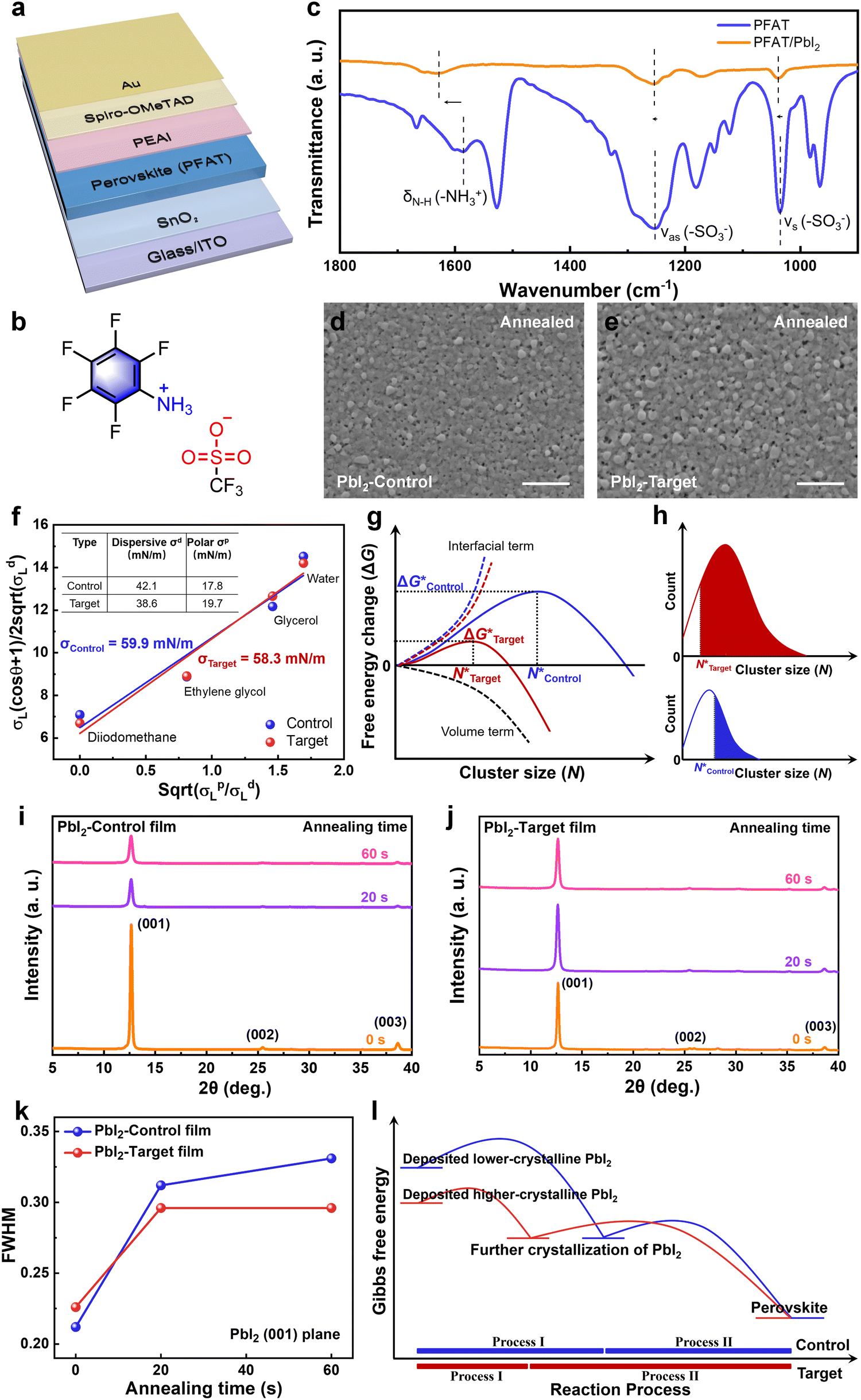 | ||
| Fig. 1 Characterization of PbI2. (a) Device architecture of as-fabricated solar cells. (b) Molecule structure of PFAT. (c) FTIR spectra of PFAT before and after mixing with PbI2. Top-view SEM images of the deposited (d) PbI2-Control and (e) PbI2-Target (i.e., 1 mg mL−1 of PFAT) annealed films. The scale bars represent 1 μm. (f) Surface tension measurements of PbI2 films w/o and with PFAT via the OWRK method. (g) Dependence of Gibbs free energy change on cluster size of the PbI2-Control and PbI2-Target films. (h) Cluster size distribution in the PbI2-Control and PbI2-Target films, therein, the fraction of the PbI2-Control clusters acting as nuclei is marked in blue and that of the PbI2-Target clusters is marked in red. XRD patterns of the (i) PbI2-Control and (j) PbI2-Target films with various annealing times at 70 °C. (k) Evolution of FWHM for (001) planes of different PbI2 films with various annealing times. (l) Gibbs free energy changes during perovskite formation. | ||
Characterization of PbI2 precursor and film properties
To begin with, we compared PbI2 precursors with and without (w/o) PFAT to check its effect on the turbidity of the PbI2 solutions (Fig. S2, ESI†). All the solutions show a distinct Tyndall effect, and no obvious difference can be seen in the PbI2 solutions. To further understand the underlying chemical interaction between PFAT and PbI2 in precursor solutions, Fourier transform infrared spectroscopy (FTIR) measurements were conducted. As shown in Fig. 1c, peaks located at 1034 and 1252 cm−1 are related to symmetrical (νs) and antisymmetric (νas) stretching vibrations of –SO3− in PFAT, respectively.33,34 After mixing with PbI2, the corresponding peaks shift to 1038 and 1254 cm−1, respectively. Besides, N–H bending vibration of –NH3+ (δN–H (–NH3+)) in PFAT appears at 1586 cm−1, which is red-shifted by 42 cm−1 after interacting with PbI2. The red shift of vibrations of –SO3− and –NH3+ indicates the inherent interaction between –SO3− and –NH3+ in PFAT becomes weaker, which means the interaction of PFAT with PbI2.35We then performed scanning electron microscopy (SEM) and atomic force microscopy (AFM) to study the effect on the morphology of the resulting PbI2 films. For the two-step sequential deposition method, spin-coated PbI2 films usually undergo an annealing process at 70 °C for about 1 min.17,36 It should be noted that this brief annealing process is indispensable because the as-deposited unannealed PbI2 films present various-size PbI2 crystals (Fig. S3a and b, ESI†). Moreover, AFM tests show that the unannealed pristine PbI2 film is very rough, and the addition of PFAT reduces the roughness (Fig. S4a and b, ESI†). As can be seen in Fig. S5a and b (ESI†), both the pristine and PFAT-processed PbI2 films present sharp protrusions at the top surface. All of these can hinder organic ammonium salts intercalate into the PbI2 plates and lead to inhomogeneous perovskite grains. Meanwhile, failure to volatilize the redundant solvents can inhibit the subsequent growth of perovskite grains. As shown in Fig. 1d and e, we can see that the morphology of the annealed PbI2 film becomes much more porous after appropriate PFAT treatment. For comparison, the pristine PbI2 film is relatively denser, which is not conducive to the penetration of ammonium salts. The much highly porous PbI2 thin film can lead to the formation of favorable α-FAPbI3.11 We speculate that the formation of the much more porous PbI2 film may arise from the pre-aggregation induced by an intermediate phase.21 The statistics of cluster sizes (Fig. S6, ESI†) show that the PbI2 clusters are significantly larger after the PFAT treatment. This facilitates the subsequent cluster growth, which will be mentioned later. The corresponding AFM tests reflect the same trend (Fig. S7a and b, ESI†). Incidentally, the brief annealing process for the PbI2 films reduces the surface roughness. Cross-sectional SEM images present that a porous trend is already present in the direction perpendicular to the substrate in the unannealed PFAT-processed film (Fig. S8a and b, ESI†). After annealing, the PbI2-Target film is more porous and looser in the longitudinal direction compared to the PbI2-Control film (Fig. S9a and b, ESI†), which provides more channels for the penetration of the ammonium salts. When excess PFAT is added, the pores become enlarged and are accompanied by deterioration of the homogeneity of PbI2 crystals (Fig. S10, ESI†), which is detrimental to the subsequent growth of perovskite grains.
The crucial thermodynamic factors affecting PbI2 nucleation are Gibbs free energy (ΔG*) and the critical cluster size (N*), which are determined by the interfacial term and the volume term (the following eqn (1) and (2)).30
 | (1) |
 | (2) |
Apart from the nucleation, the PFAT addition also has an obvious effect on the crystallinity of PbI2 films. To further understand the impact of the PFAT addition on the crystallinity of PbI2 films, X-ray diffraction (XRD) was carried out. We tested XRD patterns of the PbI2 films with various annealing times at 70 °C to analyze the change in crystallinity, as presented in Fig. 1i and j. Given the variation of the crystallinity of PbI2, the full width at half-maximum (FWHM) and peak intensity evolution of the PbI2 (001) plane with various annealing times are recorded in Fig. 1k and Fig. S13 (ESI†), respectively. Initially, the pristine PbI2 film shows a strong peak intensity and a narrow FWHM. In combination with the aforementioned results shown in Fig. S4 and S5 (ESI†), the unannealed pristine PbI2 film shows a lamellar structure with many prominent spikes, which confirm the strong crystallinity of the initial PbI2 film. However, the unsmooth surface of the unannealed PbI2 film can hinder the penetration of the ammonium salts and destroy the favorable growth of perovskite grains. The slightly higher FWHM value and the much lower peak intensity in the PbI2-Target film are probably due to the complexation of PFAT with part of PbI2. During the subsequent 20 s of annealing, the (001) peak intensity of the PbI2-Control film decreases sharply, while that of the PbI2-Target film remains almost unchanged, even though the FWHMs of both films increase. This is because the rapid evaporation of the residual solvents leads to the partial destruction of the inherent crystallinity for the pristine PbI2 film. While this phenomenon is alleviated by the interaction of PFAT with PbI2 in the PFAT-processed PbI2 film. Accompanied by further thermal annealing, the peak intensity of the control PbI2 film no longer changes owing to the solvents being evaporated at the beginning of the annealing, while the peak intensity of the target one slightly decreases as a result of the evaporation of the remaining solvent dragged by PFAT. All the final annealed PbI2 films have smoother morphology compared to the initial unannealed PbI2 films (Fig. S4 and S7, ESI†), which creates favorable conditions for the subsequent interaction of the ammonium salts, even with the compromise of the reduced crystallinity. Moreover, the PFAT-treated film maintains a lower FWHM value relative to the untreated one, which implies a higher crystallinity of the annealed PFAT-processed PbI2 film. This is very crucial for perovskite growth, since the formation of the perovskite phases does not occur immediately after the contact of the ammonium salts with PbI2, but that further crystallization of PbI2 takes place first.22,30 In other words, the higher the crystallinity of the annealed PbI2 films, the earlier the formation of the perovskite phases proceeds.
The interaction of the ammonium salts with the PbI2 is usually followed by further crystallization of the as-deposited PbI2 (named Process I) before intercalation of the ammonium salts and formation of the perovskite phases (named Process II).22,30,31 The whole processes (Process I + II) follows Ostwald's step rule, where the reaction gradually stabilizes from a metastable state at the beginning, accompanied by a decrease in Gibbs free energy.22 In that way, the formation of a higher-crystallinity PbI2 film with lower Gibbs free energy before the interaction with the ammonium salts facilitates the faster completion of Process I and then, an earlier start of Process II, which leads to adequate interaction and larger perovskite grains, as shown schematically in Fig. 1l. This indicates that the crystallinity regulation of PbI2 films by PFAT is beneficial to the growth of perovskite crystals. Considering the secondary nucleation of PbI2 clusters in the PbI2-PFAT film mentioned earlier (Fig. 1g and h), more and more highly crystalline PbI2 forms and promotes the early formation of perovskites. Thus, through the introduction of PFAT, the modulation of both nucleation and crystallization in PbI2 films promotes perovskite formation.
Morphology and photoelectrical properties of perovskite films
The XRD evolution of the deposited perovskite films with various thermal annealing times (0, 3, 9, and 13 min) was further explored. As shown in Fig. 2a and b, for the control film, the (001) peak intensity of perovskite does not change much with the annealing time increases but is accompanied by a noticeable increase in the PbI2 (001) peak intensity and an undesirable perovskite (111) orientation. The enhancement of the PbI2 (001) peak intensity can be attributed to the partial decomposition of the perovskite films with the volatilization of the ammonium salts during the annealing process.37–39 In contrast, the peak intensity of PbI2 in the target film does not change much, while the perovskite (001) peak intensity increases significantly and (111) plane diffraction peak decreases. It can be visualized that the ratio of perovskite (001)/(111) for the target film rises sharply with the annealing time increases, while that for the control one remains almost constant (Fig. 2c). In previous reports, the (001) facet is benign in perovskite growth and has a higher photoluminescence (PL) intensity, while the (111) facet tends to have a higher defect state density.17,18,40 The higher (001)/(111) ratio implicates that the preferential orientation of perovskite crystals can be modulated by doping PFAT, which helps to obtain perovskite films with higher quality and fewer defects. Remarkably, when we compare the change in the ratio of the perovskite (001) plane and PbI2 (001) plane for the two sets of films (Fig. 2d), it can be found that the ratio increases rapidly in the first 3 minutes of annealing for the target film. This is because flat and porous PbI2 films with higher crystallinity have a facile and adequate intercalation with the ammonium salts and convert more rapidly to perovskite phases, which confirms the above analysis of the section on PbI2 films. However, the pristine over-dense PbI2 film deteriorates the formation of perovskite phases. In the subsequent annealing, the slowing down of the perovskite (001)/PbI2 (001) ratio for both films may be associated with the partial volatilization of the ammonium salts induced by thermal annealing. Moreover, we can also observe that the residual PbI2 in perovskite films is greatly reduced with the incorporation of PFAT (Fig. 2a, b, and d).41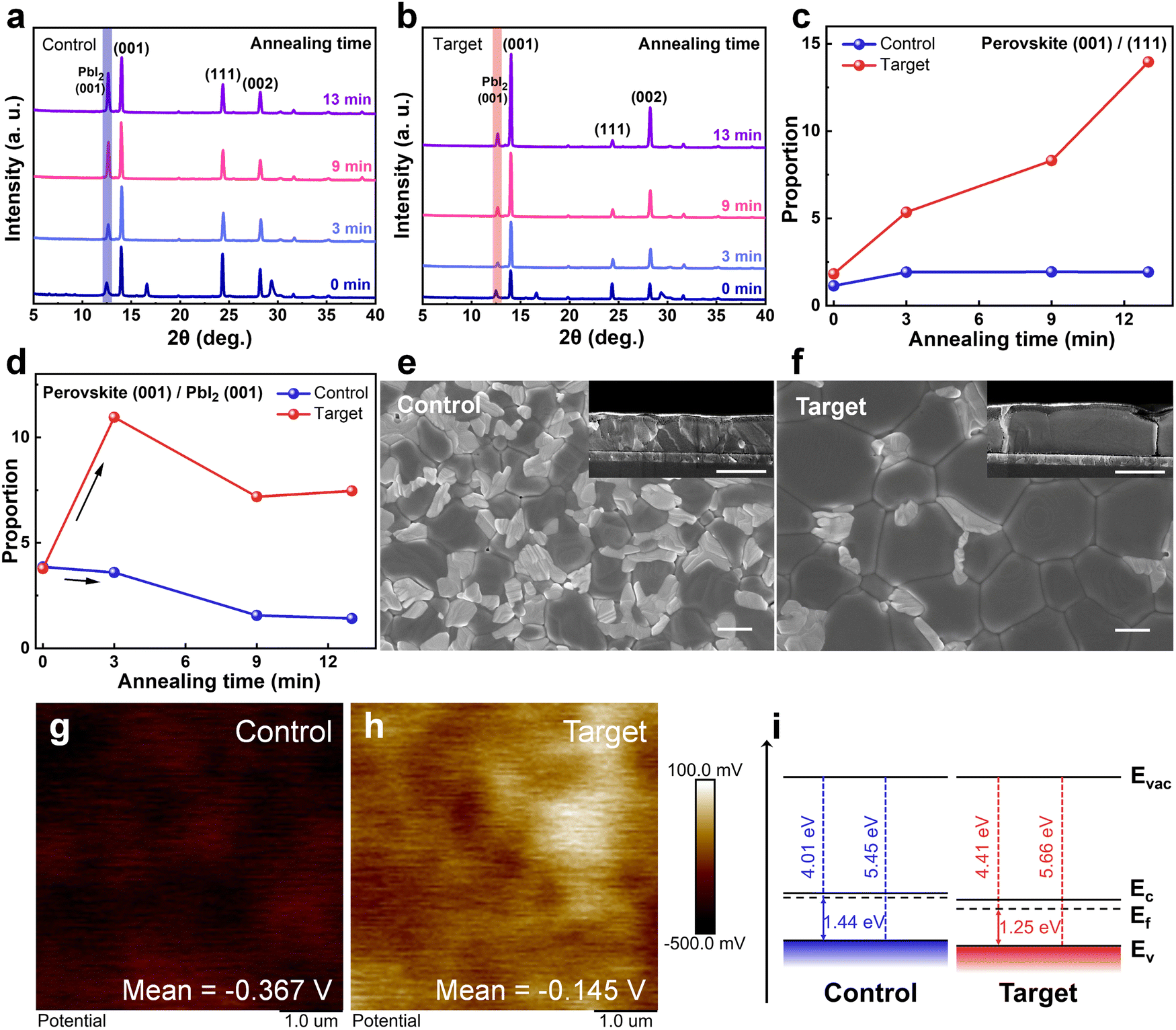 | ||
| Fig. 2 Characterization of perovskite films. XRD patterns of the (a) control and (b) target perovskite films with varied annealing time. Evolution of (c) the perovskite (001)/(111) ratio and (d) the perovskite (001)/PbI2 (001) ratio in different perovskite films. Top-view and inserted cross-sectional SEM images of perovskite films (e) before and (f) after PFAT incorporation. All scale bars are represented as 1 μm. KPFM images of perovskite films (g) w/o and (h) with PFAT. (i) Energy level diagram of different perovskite films. | ||
We then performed top-view and cross-sectional SEM measurements to verify the effect of PFAT on the growth of perovskite grains. As depicted in Fig. 2e and f, for the control perovskite film, the grains are dispersed and heterogeneous in size because of the penetration difficulty of the ammonium salts. On the contrary, the grains are much larger and interconnected for the target film, owing to the thorough penetration of the ammonium salts and the adequate interaction with PbI2, which reduce perovskite grain boundaries and further diminish non-radiative recombination. From the cross-sectional SEM images (insets of Fig. 2e and f), one can see that the PFAT-treated perovskite film has larger grains in size and volume and grows perpendicular to the substrate, while the untreated film is irregular in the longitudinal direction. The preferred vertical growth orientation of the PFAT-treated perovskite film is conducive to charge transport and extraction. Consistent with the XRD results, the SEM images also present that the residual PbI2 in perovskite films is greatly reduced with the incorporation of PFAT, especially for that at the grain boundaries (Fig. 2e and f). In addition, the reduction of excess PbI2 within perovskites would benefit the stability of perovskite films and devices.41
AFM and Kelvin probe force microscopy (KPFM) were utilized to test the surface roughness and potential of perovskite films. For both the perovskite films w/o and with PFAT, there is no significant change in roughness (Fig. S14a and b, ESI†), yet the surface potential of the two samples differs considerably (Fig. 2g and h). The surface potential of the target film (−0.145 V) is increased by 222 mV with respect to that of the control one (−0.367 V). The apparently higher surface potential implies a downward shift in the Fermi energy level of the PFAT-treated perovskite film surface, which would facilitate carrier extraction.42 A highly oriented pyrolytic graphite (HOPG) was used as a standard sample to calibrate the values of Fermi energy levels of perovskite films (Fig. S15, ESI†). Based on the KPFM results, the Fermi energy levels of the control and target films are estimated to be around −3.994 and −4.216 eV (see ESI† Note S2 for details), respectively. Ultraviolet photoelectron spectroscopy (UPS) was then employed to validate Fermi energy levels and valence band maximums (VBMs) of the two films (Fig. S16, ESI†). The energy level diagram was drawn on the basis of the UPS results, as shown in Fig. 2i. The Fermi levels of the control and target films are determined to be 4.01 and 4.41 eV as well as VBMs of −5.45 and −5.66 eV, respectively, which nearly coincide with the KPFM results. The deeper VBM of PFAT-tailored perovskite contributes to higher open-circuit voltage (VOC) of devices,42–45 which can be evidenced later.
The optical properties of perovskite films were then investigated by ultraviolet-visible (UV-vis) absorption spectra (Fig. S17, ESI†). The markedly enhanced absorption of the target perovskite film can be ascribed to its better orientation and extended grain size and volume (insets in Fig. 2e and f). In addition, compared to that of the control one, the bandgap of the target one becomes slightly wider (Fig. S18, ESI†), which may be attributed to the presence of the large cation in PFAT. Transient absorption (TA) spectroscopic measurements were then employed to distinguish the carrier transport dynamics in the control and target perovskite films, as shown in Fig. 3a and b. Upon excitation of a sample with a 400 nm pump light, electrons in the ground state absorb photons and jump to the excited state, reducing the number of electrons in the ground state. The reduced absorption of a probe light by the excited sample allows a negative ΔA signal to be detected, i.e., a ground-state bleaching (GSB) signal.46,47 There is a slight blue shift in the GSB peak position of the target film (784.2 nm) compared to that of the control one (785.8 nm) because of the slightly wider bandgap (Fig. S18, ESI†). The variation of the GSB peaks with decay time is shown in Fig. S19 (ESI†), and the fitted data are summarized in Table S2 (ESI†). The carrier lifetime τ2 increases from 7613.3 ps to 11293.4 ps after PFAT addition, indicating decreased carrier recombination in the target film.41,48 Steady-state photoluminescence (PL) and time-resolved photoluminescence (TRPL) were also measured to compare carrier transport dynamics in different perovskite films. The PFAT-processed perovskite film shows a stronger PL emission and longer PL decay lifetime than the control film, owing to the suppression of non-radiative recombination (Fig. 3c and d and Table S3, ESI†). The slight blue shift conforms to the change in bandgap obtained from the absorption results (Fig. S18, ESI†). For both glass/SnO2/perovskite and glass/perovskite/spiro-OMeTAD structures, the stronger PL quenching of the target film illustrates better electron and hole extraction ability relative to that of the control one (Fig. S20, ESI†). We also employed a confocal laser scanning fluorescence microscopy (CLSM) to examine the PL mapping of the samples. As viewed in Fig. 3e and f, for the pristine perovskite film, the uneven and weak PL distribution implies poor crystalline quality. After PFAT addition, much more homogeneous and brighter PL emissions and larger perovskite grains observed in the target film confirm the significantly improved crystallinity and reduced non-radiative recombination of the sample.41
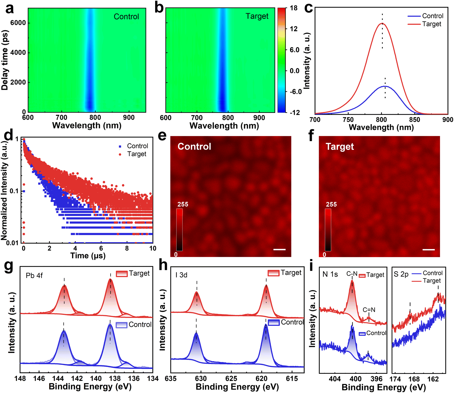 | ||
| Fig. 3 Optoelectronic properties of perovskite films. Pseudo color maps of TA spectra for the (a) control and (b) target perovskite films upon excitation at 400 nm. (c) Steady-state PL, and (d) TRPL spectra of the control and target perovskite films deposited on glass substrates. PL mapping images of the perovskite films under CLSM (e) w/o and (f) with PFAT treatment. The scale bars represent 1 μm. (g) Pb 4f, (h) I 3d, (i) N 1s, and S 2p spectra of perovskite films w/o and with PFAT incorporation. | ||
Underlying mechanism explanation
X-Ray photoemission spectroscopy (XPS) was utilized to explore the chemical interaction on the surface of perovskite films. The full XPS spectra of different perovskite films are displayed in Fig. S21 (ESI†). The detailed Pb 4f and I 3d spectra of the target film simultaneously show a slight shift of the peak position toward smaller binding energy (Fig. 3g and h), implying the interaction of PFAT with Pb-I octahedra. The –SO3− in PFAT interacts with the uncoordinated Pb,49,50 while –NH3+ donates a lone pair of electrons to positively charged iodine vacancies for defect healing.51,52 The attenuated Pb0 peaks imply the reduction of residual PbI2, which can further decompose into harmful Pb0 impurities by light excitation.41 The elevated ratio of C–N/C![[double bond, length as m-dash]](https://www.rsc.org/images/entities/char_e001.gif) N in the N 1s peaks and the appearance of the S 2p peaks in Fig. 3i signify that both the cation (with C–N) and anion (with S element) of PFAT are present in the perovskite films after PFAT processing, rather than volatilizing with thermal annealing.
N in the N 1s peaks and the appearance of the S 2p peaks in Fig. 3i signify that both the cation (with C–N) and anion (with S element) of PFAT are present in the perovskite films after PFAT processing, rather than volatilizing with thermal annealing.
With the above characterizations, we construct schematic diagrams to describe potential mechanisms of the underlying perovskite crystal growth (Fig. 4). Generally, after annealing at 70 °C, PbI2 films have both amorphous domains and PbI2 clusters.30–32 For the control sets (Fig. 4a–c), initially, the PbI2 clusters are small and the crystallinity is relatively low. When the ammonium salt solutions are dropped on the PbI2-Control films with low crystallinity and small crystalline clusters, clusters whose sizes do not reach the critical N*Control cannot grow further, and PbI2 in the amorphous domains is transported to the larger clusters (cluster sizes > N*Control) to promote their secondary growth. Then, only a small amount of PbI2 clusters reach a critical crystallinity and the ammonium salts begin to interact with them. The slow consumption of PbI2 leads to increased residual PbI2 and the formation of an undesirable perovskite (111) plane, which eventually brings about small grains and many defects. In contrast, for the target sets (Fig. 4d–f), the PbI2 clusters are larger and have relatively higher crystallinity in the PbI2-Target films initially. When the ammonium salts start to contact PbI2, more PbI2 clusters undergo their secondary nucleation because of N*Target < N*Control (Fig. 1g and h), which has been mentioned earlier. The large clusters that reach the critical crystallinity start to interact with the ammonium salts to form perovskite phases, and the slightly smaller clusters consume amorphous domains to achieve the desired crystallinity. As the interaction continues, more PbI2 clusters begin to be converted to perovskites. Then, more PbI2 is consumed and a more optimal orientation of a perovskite (001) facet is obtained in the target ones, owing to the higher crystallinity of the PbI2 films with large clusters. Note that when the PbI2 films are in contact with the ammonium salts, the whole thermodynamic system is metastable at the beginning and spontaneously tends to a steady state until the final conversion to perovskites, accompanied by a reduction of Gibbs free energy of the whole system, which follows Ostwald's step rule. In addition, the –NH3+ and –SO3− terminal groups in PFAT can further passivate inherent defects in perovskite films.13,35,53 The –NH3+ passivates positively charged iodine vacancies by delivering a lone pair of electrons, and the –SO3− can interact with undercoordinated Pb2+ ions.
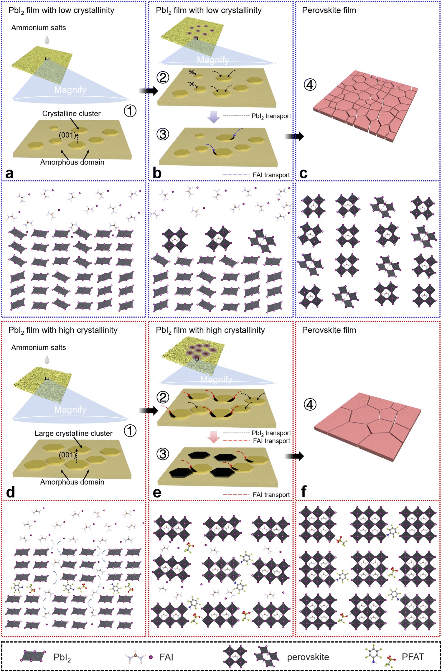 | ||
| Fig. 4 Underlying mechanism explanations. Schematic diagrams of the interaction of dripped organic ammonium salts with the deposited PbI2 films (a–c) w/o and (d–f) with PFAT and the formation of perovskite crystals. For simplicity, the ammonium salts are replaced by FAI. (a) The small clusters with low crystallinity. (b) A small number of clusters start the secondary growth and convert to perovskite phases, accompanied by the formation of undesired perovskite (111) facets and PbI2 residue. (c) The perovskite film with small grains and an unwanted (111) orientation. (d) The large clusters with high crystallinity. (e) The conversion of perovskite phases occurs and clusters with sizes larger than N*Target commence the secondary growth and then interact with the ammonium salts. (f) The perovskite film with large grains and a preferential orientation. | ||
Device performance, defect characterization, and stability studies
The operation performance statistics of the control and PFAT-processed devices are presented in Fig. 5a. Obviously, PFAT doping leads to a significant increase in the VOC and FF of PSCs, which promotes an effective increment in PCE. The average (champion) PCE, VOC, FF, and the short-circuit current density (JSC) for the target devices without antireflective films are 22.77 ± 0.23% (23.13%), 1.163 ± 0.005 V (1.171 V), 81.69 ± 0.14% (81.86%), and 23.98 ± 0.20 mA cm−2 (24.28 mA cm−2), respectively, while those for the control cells without antireflective films are 22.10 ± 0.22% (22.42%), 1.143 ± 0.002 V (1.146 V), 80.55 ± 0.54% (81.16%), and 24.00 ± 0.24 mA cm−2 (24.33 mA cm−2), respectively. Polydimethylsiloxane (PDMS) antireflective films were also pasted on the glass substrates of the PFAT-processed PSCs to reduce the reflection light on the glass side, thus significantly increasing the JSC of the devices (Fig. S22, ESI†). The best-performing PFAT-treated PSC with a PDMS antireflective coating gives an impressive PCE of 24.52% with a much-enhanced VOC of 1.164 V, an FF of 82.84%, and a JSC of 25.43 mA cm−2 (Fig. 5b), which is one of the highest PCEs in two-step sequential deposition-processed PSCs so far. The data of the forward and reverse sweeps of the corresponding device is also ordered (Fig. S23 and inset therein, ESI†). Depending on the external quantum efficiency (EQE) spectrum (Fig. 5c), the integrated current density of the target device is 25.27 mA cm−2, which coincides with the JSC obtained from the J–V curve (Fig. 5b). Steady power output (SPO) test (Fig. 5d) shows that the PFAT-processed device maintains a steady-state PCE of approximately 24.3% at a bias voltage of 0.99 V for 200 s. For comparison, the relevant parameters for the best-performing control cell are placed in Fig S24 (ESI†).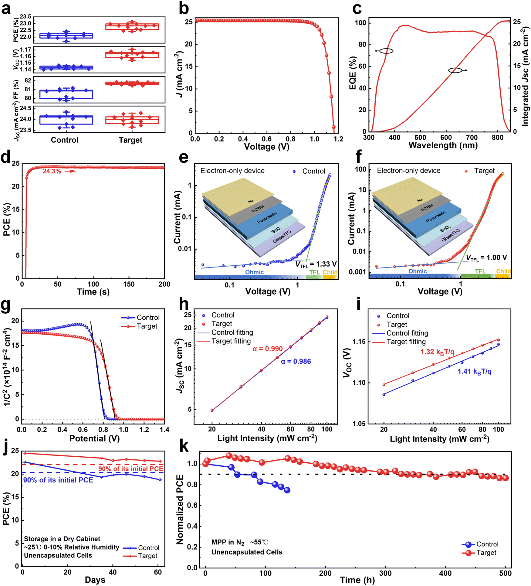 | ||
| Fig. 5 Photovoltaic performance and stability of PSCs. (a) Statistical distribution charts of the photovoltaic parameters for the control and PFAT-processed devices. (b) J–V curve of the best-performing target device, which includes an antireflective film to increase the JSC. (c) EQE spectrum and integrated curve of the best-performing target cell. (d) SPO test of the best-performing target device measured at a constant bias voltage of 0.99 V within 200 s. SCLC measurements for the electron-only (e) control and (f) target devices. (g) Mott–Schottky curves for different PSCs. The dependence of (h) JSC and (i) VOC on light intensity for devices. (j) PCE decay of the best-performing control and target PSCs in a dry cabinet (∼25 °C, 0–10% relative humidity) in the dark. (k) MPP tracking of the unencapsulated cells under constant light exposure at ∼55 °C in an N2-filled glovebox. | ||
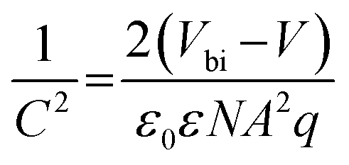
Space-charge-limited current (SCLC) characterization was conducted to compare the trap density (Nt) of electrons and holes (Fig. 5e and f and Fig. S25a and b, ESI†) for different samples by using electron-only and hole-only devices, respectively.54,55 For the electron-only devices, the trap-filled limited voltage (VTFL) of the target cell is around 1.00 V, which can be calculated as Nt = 3.6 × 1015 cm−3, whereas that of the control one is around 1.33 V (Nt = 4.8 × 1015 cm−3). As for the hole-only devices, the derived Nt equals 1.4 × 1015 cm−3 for the control device (VTFL = 0.39 V), while the Nt of the PFAT-tailored cell is only 1.0 × 1015 cm−3 (VTFL = 0.28 V). The reduced density of defect states for both electrons and holes for the target device can be ascribed to a preferred crystalline orientation, lowered defects, and enlarged grains. We then measured Mott–Schottky curves (Fig. 5g) to investigate the variation of the built-in electric field in PSCs, which can be estimated by the following formula:
 | (3) |
We then tested and compared the long-term storage and light stability of the control and target devices. The devices were placed in a dry cabinet (∼25 °C, 0–10% relative humidity) in the dark for long-term storage stability measurements (Fig. 5j). The initial PCEs of the control and target devices were 22.60% and 24.52%, respectively. After 61 days of storage, the efficiency of the target group remained above 90% of its initial efficiency, while the efficiency of the control group fell below 90% of its initial efficiency within 35 days, demonstrating much better storage stability after the PFAT treatment. Maximum power point (MPP) tracking at an operating temperature of ∼55 °C was utilized to further monitor the long-term photostability of PSCs in an N2 atmosphere. As shown in Fig. 5k, after 500 hours of constant light exposure, the target cell maintained ∼90% of its initial efficiency, in contrast to the control PSC, which dropped to ∼75% of its initial PCE after only 136 hours of constant light illumination. All these results indicate that the PFAT treatment improves the operation and photostability of the devices, which can be attributed to the enhanced crystalline quality, decreased surplus PbI2, and reduced defects of as-fabricated perovskite films.
Conclusion
In summary, by using PFAT to modulate the morphology, nucleation, and crystallinity of PbI2 films, we obtained preferentially oriented perovskite films with a largely reduced amount of residual PbI2. The incorporation of PFAT allows for the effective intercalation of organic ammonium salts. The secondary nucleation of larger PbI2 clusters and the enhanced crystallinity of PbI2 films enable the organic salts to interact with PbI2 earlier. Besides, the multi-functional groups in PFAT can passivate inherent defects in perovskite films through Lewis acid-base interactions. All of these reasons contribute to high-quality perovskite films with enlarged grains, reduced defects, and favored crystal growth of perovskites perpendicular to the substrates. The homogeneous growth of perovskites ultimately affords solar cells with a striking PCE of 24.52%, accompanied by significantly improved storage and MPP stability. This work provides a way to achieve favorable growth of perovskites and optimize the operational performance and stability of devices by pre-modulating PbI2 precursor films.Experimental
Materials and reagents
PbI2 (99.9985%) and lithium bis(trifluoromethanesulfonyl)imide (Li-TFSI) were bought from Tokyo Chemical Industry (TCI, Japan). PFAT was purchased from Macklin. PEAI was purchased from Xi’an Polymer Light Technology. Formamidinium iodide (FAI), methylammonium iodide (MAI), and spiro-OMeTAD (99%) were bought from Advanced Election Technology CO., Ltd. Methylammonium chloride (MACl) was purchased from Sigma Aldrich. SnO2 colloid solution (15 wt%) was bought from Alfa-Aesar. Hydrogen peroxide aqueous solution (H2O2, 30%) was purchased from Sinopharm Chemical Reagent Co., Ltd. N,N-dimethylformamide (DMF, 99.8%), dimethyl sulfoxide (DMSO, 99.9%), isopropanol (IPA) (99.7%), chlorobenzene (CB 99.8%), 4-tert-butylpyridine (tBP), and acetonitrile (ACN, 99.9%) were also purchased from Sigma-Aldrich.Device fabrication
SnO2 colloid solution was diluted with DI water and H2O2 aqueous solution (1![[thin space (1/6-em)]](https://www.rsc.org/images/entities/char_2009.gif) :4:1, v:v:v) and stirred at room temperature for 1 hour. The mixed aqueous solution was spin-coated onto the glass/ITO substrates at 4000 rpm for 30 s and then the substrates were annealed at 180 °C for 25 min in ambient air. To prepare the precursor solutions for the perovskite layers, 1.4 M PbI2 solutions (DMF/DMSO, v:v = 9:1) with different concentrations of PFAT (0, 0.5, 1, and 2 mg mL−1) were stirred at 70 °C for 6 hours, and organic ammonium salt solutions (FAI:MACl:MAI = 60 mg:10 mg:10 mg in 1 mL IPA) were stirred at room temperature for 6 h. In an N2-filled glove box, PbI2 solutions were spin-coated onto the deposited SnO2 layers at 1500 rpm for 30 s and immediately transferred to a hot plate for annealing at 70 °C for 1 min. After cooling, 100 μL of organic ammonium salt solutions were then rapidly poured down and spin-coated at 1800 rpm for 30 s. The substrates were transferred to a hot table in ambient air (30–40% relative humidity) to anneal at 150 °C for 15 min. For the passivation treatment, a PEAI solution (2 mg mL−1 in IPA) was deposited on the cooled-down perovskite films at 5000 rpm for 30 s without further annealing in an N2-filled glove box. A stock spiro-OMeTAD solution consisting of 72.3 mg in 1 mL of CB with 28.8 μL of tBP and 17.5 μL of Li-TFSI solution (520 mg of Li-TFSI powder in 1 mL of ACN) was then coated on the modified-perovskite films at 3000 rpm for 30 s. After at least 8 hours of oxidation in a dry cabinet, 60 nm of Au was thermally evaporated at 2 × 10⁻⁴ Pa. PDMS antireflection films were pasted on the glass substrates to increase light collection.
:4:1, v:v:v) and stirred at room temperature for 1 hour. The mixed aqueous solution was spin-coated onto the glass/ITO substrates at 4000 rpm for 30 s and then the substrates were annealed at 180 °C for 25 min in ambient air. To prepare the precursor solutions for the perovskite layers, 1.4 M PbI2 solutions (DMF/DMSO, v:v = 9:1) with different concentrations of PFAT (0, 0.5, 1, and 2 mg mL−1) were stirred at 70 °C for 6 hours, and organic ammonium salt solutions (FAI:MACl:MAI = 60 mg:10 mg:10 mg in 1 mL IPA) were stirred at room temperature for 6 h. In an N2-filled glove box, PbI2 solutions were spin-coated onto the deposited SnO2 layers at 1500 rpm for 30 s and immediately transferred to a hot plate for annealing at 70 °C for 1 min. After cooling, 100 μL of organic ammonium salt solutions were then rapidly poured down and spin-coated at 1800 rpm for 30 s. The substrates were transferred to a hot table in ambient air (30–40% relative humidity) to anneal at 150 °C for 15 min. For the passivation treatment, a PEAI solution (2 mg mL−1 in IPA) was deposited on the cooled-down perovskite films at 5000 rpm for 30 s without further annealing in an N2-filled glove box. A stock spiro-OMeTAD solution consisting of 72.3 mg in 1 mL of CB with 28.8 μL of tBP and 17.5 μL of Li-TFSI solution (520 mg of Li-TFSI powder in 1 mL of ACN) was then coated on the modified-perovskite films at 3000 rpm for 30 s. After at least 8 hours of oxidation in a dry cabinet, 60 nm of Au was thermally evaporated at 2 × 10⁻⁴ Pa. PDMS antireflection films were pasted on the glass substrates to increase light collection.
Characterizations
FTIR spectra were obtained by a NICOLET 5700 FTIR Spectrometer in the wavenumber range of 900–4000 cm−1. The morphology of the films was visualized by a JSM 6700F field emission scanning electron microscope (FE-SEM) with an accelerating voltage of 15 kV. XRD patterns were attained by an X-ray diffraction instrument (SmartLab-3kW, Rigaku, Japan) with a scan speed of 5 degrees min−1. TA spectra were obtained from an Ultrafast System HELIOSTM TA spectrometer. AFM and KPFM images were observed by a Bruker Dimension Icon XR equipment in a Scanasyst-Air and Peak force KPFM Mode. UV-vis absorption spectra were measured by a SHIMADZU mini 1280 UV-visible spectrophotometer. Steady-state PL and TRPL of the perovskite films were recorded by a HORIBA Jobin Yvon IBH Ltd with a 481 nm laser and a time-correlated single-photon counting module. PL mapping was captured by a confocal laser scanning fluorescence microscopy (CLSM) (TCS SP8, Leica). A 552 nm laser was applied as the PL excitation source to detect and collect the PL signals at 700–800 nm, and the scale range collected on the perovskite films was 10 μm × 10 μm. UPS and XPS measurements were carried out by an ESCALAB 250Xi (Thermo Fisher Scientific, USA). J–V curves, SCLC, and steady-state power output measurements were scanned and recorded by a Keithley 2400 Source Meter with a Newport 94023A solar simulator. Before each time J–V measurement, the light intensity of the solar simulator was calibrated by a National Renewable Energy Laboratory-certified and KG5-filtered crystalline silicon solar cell. The mismatch factor was 1.0. The active region (0.1188 cm2) of the devices was covered by a mask with an aperture area of 0.0557 cm2. EQE spectra were collected by a QE system (Enli Technology Co., Ltd). Electrochemical impedance spectra (EIS) were tested by a CHI760E electrochemical workstation (Shanghai Chenhua Instruments, Inc). MPP tracking data measured under light illumination (a white LED light source with 70 mW cm−2) were recorded with a multi-channel testing system (Suzhou D & R Instruments). The unencapsulated cells were placed in an N2-filled glove box and the operational temperature is about 55 °C.Author contributions
Conceptualization, W. S.; methodology, W. S.; investigation, W. S.; formal analysis, W. S., H. W., F. Y., C. W., C. W., H. C., K. D., Y. G., and T. W.; funding acquisition, W. K., and G. F.; project administration, G. F.; resources, W. S.; validation, W. S.; visualization, W. S.; writing – original draft, W. S.; writing – review & editing, W. S., W. K., and G. F.; supervision, W. K., and G. F.Conflicts of interest
There are no conflicts to declare.Acknowledgements
This work was supported by the National High Technology Research and Development Program (grant number 2015AA050601), the National Natural Science Foundation of China (grant numbers 12134010 and 12174290), the Natural Science Foundation of Hubei Province, China (grant number 2021CFB039), the Shenzhen Fundamental Research Program (grant number JCYJ20190808152609307), and Guangdong Basic and Applied Basic Research Foundation (grant number 2022A1515011931). We thank the Core Facility of Wuhan University for SEM and FTIR analysis.References
- NREL, Best research-cell efficiencies, (accessed September, 2022), https://www.nrel.gov/pv/cell-efficiency.html.
- M. Kim, J. Jeong, H. Lu, K. Lee Tae, T. Eickemeyer Felix, Y. Liu, W. Choi In, J. Choi Seung, Y. Jo, H.-B. Kim, S.-I. Mo, Y.-K. Kim, H. Lee, G. An Na, S. Cho, R. Tress Wolfgang, M. Zakeeruddin Shaik, A. Hagfeldt, Y. Kim Jin, M. Grätzel and S. Kim Dong, Science, 2022, 375, 302–306 CrossRef CAS PubMed.
- J. Jeong, M. Kim, J. Seo, H. Lu, P. Ahlawat, A. Mishra, Y. Yang, M. A. Hope, F. T. Eickemeyer, M. Kim, Y. J. Yoon, I. W. Choi, B. P. Darwich, S. J. Choi, Y. Jo, J. H. Lee, B. Walker, S. M. Zakeeruddin, L. Emsley, U. Rothlisberger, A. Hagfeldt, D. S. Kim, M. Gratzel and J. Y. Kim, Nature, 2021, 592, 381–385 CrossRef CAS PubMed.
- H. Lu, Y. Liu, P. Ahlawat, A. Mishra, W. R. Tress, F. T. Eickemeyer, Y. Yang, F. Fu, Z. Wang, C. E. Avalos, B. I. Carlsen, A. Agarwalla, X. Zhang, X. Li, Y. Zhan, S. M. Zakeeruddin, L. Emsley, U. Rothlisberger, L. Zheng, A. Hagfeldt and M. Grätzel, Science, 2020, 370, eabb8985 CrossRef CAS PubMed.
- H. Min, M. Kim, S.-U. Lee, H. Kim, G. Kim, K. Choi, H. Lee Jun and I. Seok Sang, Science, 2019, 366, 749–753 CrossRef CAS PubMed.
- G. Kim, H. Min, S. Lee Kyoung, Y. Lee Do, M. Yoon So and I. Seok Sang, Science, 2020, 370, 108–112 CrossRef CAS PubMed.
- Y. Zhang, Y. Li, L. Zhang, H. Hu, Z. Tang, B. Xu and N. G. Park, Adv. Energy Mater., 2021, 11, 2102538 CrossRef CAS.
- Z. Liu, P. Liu, M. Li, T. He, T. Liu, L. Yu and M. Yuan, Adv. Energy Mater., 2022, 12, 2200111 CrossRef CAS.
- C. Liu, J. Zhang, L. Zhang, X. Zhou, Y. Liu, X. Wang and B. Xu, Adv. Energy Mater., 2022, 12, 2200945 CrossRef CAS.
- C. Chen, Y. Lou, K. Wang, Z. Su, C. Dong, J. Chen, Y. Shi, X. Gao and Z. Wang, Adv. Energy Mater., 2021, 11, 2101538 CrossRef CAS.
- P. Ahlawat, A. Hinderhofer, A. Alharbi Essa, H. Lu, A. Ummadisingu, H. Niu, M. Invernizzi, M. Zakeeruddin Shaik, M. I. Dar, F. Schreiber, A. Hagfeldt, M. Grätzel, U. Rothlisberger and M. Parrinello, Sci. Adv., 2021, 7, eabe3326 CrossRef CAS PubMed.
- S. Chen, X. Xiao, B. Chen, L. Kelly Leah, J. Zhao, Y. Lin, F. Toney Michael and J. Huang, Sci. Adv., 2021, 7, eabb2412 CrossRef CAS PubMed.
- Z. Qin, Y. Chen, X. Wang, N. Wei, X. Liu, H. Chen, Y. Miao and Y. Zhao, Adv. Mater., 2022, 34, 2203143 CrossRef CAS PubMed.
- X. Luo, Z. Shen, Y. Shen, Z. Su, X. Gao, Y. Wang, Q. Han and L. Han, Adv. Mater., 2022, 34, 2202100 CrossRef CAS PubMed.
- J. Lu, T. Yang, T. Niu, N. Bu, Y. Zhang, S. Wang, J. Fang, X. Chang, T. Luo, J. Wen, Y. Yang, Z. Ding, K. Zhao and S. Liu, Energy Environ. Sci., 2022, 15, 1144–1155 RSC.
- X. Zhu, S. Yang, Y. Cao, L. Duan, M. Du, J. Feng, Y. Jiao, X. Jiang, Y. Sun, H. Wang, S. Zuo, Y. Liu and S. Liu, Adv. Energy Mater., 2022, 12, 2103491 CrossRef CAS.
- C. Luo, G. Zheng, F. Gao, X. Wang, Y. Zhao, X. Gao and Q. Zhao, Joule, 2022, 6, 240–257 CrossRef CAS.
- L. Zhang, Y. Liu, X. Ye, Q. Han, C. Ge, S. Cui, Q. Guo, X. Zheng, Z. Zhai and X. Tao, Cryst. Growth Des., 2018, 18, 6652–6660 CrossRef CAS.
- J. Wang, L. Yuan, H. Luo, C. Duan, B. Zhou, Q. Wen and K. Yan, Chem. Eng. J., 2022, 446, 136968 CrossRef CAS.
- W. Chen, S. Liu, Q. Li, Q. Cheng, B. He, Z. Hu, Y. Shen, H. Chen, G. Xu, X. Ou, H. Yang, J. Xi, Y. Li and Y. Li, Adv. Mater., 2022, 34, 2110482 CrossRef CAS PubMed.
- T. Zhou, Z. Xu, R. Wang, X. Dong, Q. Fu and Y. Liu, Adv. Mater., 2022, 34, 2200705 CrossRef CAS PubMed.
- A. Ummadisingu and M. Grätzel, Sci. Adv., 2018, 4, e1701402 CrossRef PubMed.
- X. Duan, X. Li, L. Tan, Z. Huang, J. Yang, G. Liu, Z. Lin and Y. Chen, Adv. Mater., 2020, 32, 2000617 CrossRef CAS PubMed.
- Y. Zhao, X. Zhang, X. Han, C. Hou, H. Wang, J. Qi, Y. Li and Q. Zhang, Chem. Eng. J., 2021, 417, 127912 CrossRef CAS.
- Z. Liu, K. Deng, Y. Zhu, M. Wang and L. Li, Solar RRL, 2018, 2, 1800230 CrossRef.
- Z. Shen, Q. Han, X. Luo, Y. Shen, T. Wang, C. Zhang, Y. Wang, H. Chen, X. Yang, Y. Zhang and L. Han, Energy Environ. Sci., 2022, 15, 1078–1085 RSC.
- W. Zhang, J. Du, W. Zhang, Y. Chu, A. Mei, Y. Rong, X. Gao, H. Han and Y. Hu, J. Energy Chem., 2022, 69, 253–260 CrossRef CAS.
- Y. Zhang, Y. Wang, X. Yang, L. Zhao, R. Su, J. Wu, D. Luo, S. Li, P. Chen, M. Yu, Q. Gong and R. Zhu, Adv. Mater., 2022, 34, 2107420 CrossRef CAS PubMed.
- F. Wang, P. Wai-Keung Fong, Z. Ren, H.-L. Xia, K. Zhou, K. Wang, J. Zhu, X. Huang, X.-Y. Liu, H. Wang, Y. Shi, H. Lin, Q. Zhu, G. Li and H. Hu, J. Energy Chem., 2022, 73, 599–606 CrossRef CAS.
- A. Ummadisingu, L. Steier, J. Y. Seo, T. Matsui, A. Abate, W. Tress and M. Gratzel, Nature, 2017, 545, 208–212 CrossRef CAS PubMed.
- H. A. Harms, N. Tétreault, N. Pellet, M. Bensimon and M. Grätzel, Faraday Discuss., 2014, 176, 251–269 RSC.
- F. Liu, F. Sommer, C. Bos and E. J. Mittemeijer, Int. Mater. Rev., 2007, 52, 193–212 CrossRef CAS.
- K. Liu, Q. Liang, M. Qin, D. Shen, H. Yin, Z. Ren, Y. Zhang, H. Zhang, P. W. K. Fong, Z. Wu, J. Huang, J. Hao, Z. Zheng, S. K. So, C.-S. Lee, X. Lu and G. Li, Joule, 2020, 4, 2404–2425 CrossRef CAS.
- J. Zhu, Y. Qian, Z. Li, O. Y. Gong, Z. An, Q. Liu, J. H. Choi, H. Guo, P. J. Yoo, D. H. Kim, T. K. Ahn, G. S. Han and H. S. Jung, Adv. Energy Mater., 2022, 12, 2200632 CrossRef CAS.
- Y. Li, Z. Chen, B. Yu, S. Tan, Y. Cui, H. Wu, Y. Luo, J. Shi, D. Li and Q. Meng, Joule, 2022, 6, 676–689 CrossRef CAS.
- Q. Jiang, Z. Chu, P. Wang, X. Yang, H. Liu, Y. Wang, Z. Yin, J. Wu, X. Zhang and J. You, Adv. Mater., 2017, 29, 1703852 CrossRef PubMed.
- F. Ye, J. Ma, C. Chen, H. Wang, Y. Xu, S. Zhang, T. Wang, C. Tao and G. Fang, Adv. Mater., 2020, 33, 2007126 CrossRef PubMed.
- H. Wang, F. Ye, J. Liang, Y. Liu, X. Hu, S. Zhou, C. Chen, W. Ke, C. Tao and G. Fang, Joule, 2022, 6, 1–16 CrossRef.
- Q. Chen, H. Zhou, T.-B. Song, S. Luo, Z. Hong, H.-S. Duan, L. Dou, Y. Liu and Y. Yang, Nano Lett., 2014, 14, 4158–4163 CrossRef CAS PubMed.
- D. Kim, J.-H. Yun, M. Lyu, J. Kim, S. Lim, J. S. Yun, L. Wang and J. Seidel, J. Phys. Chem. C, 2019, 123, 14144–14151 CrossRef CAS.
- J. Liang, X. Hu, C. Wang, C. Liang, C. Chen, M. Xiao, J. Li, C. Tao, G. Xing, R. Yu, W. Ke and G. Fang, Joule, 2022, 6, 816–833 CrossRef CAS.
- J. Wang, H. Ma, A. Wang, Z. Li, J. Dong, Y. Liu, S. Gao, S. Yan, X. Chen, Y. Li, Z. Wu, W. Xu, F. Liu, F. Wang, W. Huang and T. Qin, Matter, 2022, 5, 1–16 CrossRef.
- R. Wang, J. Xue, K. Wang, Z. Wang, Y. Luo, D. Fenning, G. Xu, S. Nuryyeva, T. Huang, Y. Zhao, L. Yang Jonathan, J. Zhu, M. Wang, S. Tan, I. Yavuz, N. Houk Kendall and Y. Yang, Science, 2019, 366, 1509–1513 CrossRef CAS PubMed.
- H. Zhu, Y. Ren, L. Pan, O. Ouellette, F. T. Eickemeyer, Y. Wu, X. Li, S. Wang, H. Liu, X. Dong, S. M. Zakeeruddin, Y. Liu, A. Hagfeldt and M. Grätzel, J. Am. Chem. Soc., 2021, 143, 3231–3237 CrossRef CAS PubMed.
- Q. Jiang, Z. Ni, G. Xu, Y. Lin, P. N. Rudd, R. Xue, Y. Li, Y. Li, Y. Gao and J. Huang, Adv. Mater., 2020, 32, 2001581 CrossRef CAS PubMed.
- H. Liu, Z. Zhang, Z. Su, W. Zuo, Y. Tang, F. Yang, X. Zhang, C. Qin, J. Yang, Z. Li and M. Li, Adv. Sci., 2022, 9, 2105739 CrossRef CAS PubMed.
- J. Qing, X.-K. Liu, M. Li, F. Liu, Z. Yuan, E. Tiukalova, Z. Yan, M. Duchamp, S. Chen, Y. Wang, S. Bai, J.-M. Liu, H. J. Snaith, C.-S. Lee, T. C. Sum and F. Gao, Adv. Energy Mater., 2018, 8, 1800185 CrossRef.
- J. Zhang, J. Qin, M. Wang, Y. Bai, H. Zou, J. K. Keum, R. Tao, H. Xu, H. Yu, S. Haacke and B. Hu, Joule, 2019, 3, 3061–3071 CrossRef CAS.
- Y. Cai, J. Cui, M. Chen, M. Zhang, Y. Han, F. Qian, H. Zhao, S. Yang, Z. Yang, H. Bian, T. Wang, K. Guo, M. Cai, S. Dai, Z. Liu and S. Liu, Adv. Funct. Mater., 2021, 31, 2005776 CrossRef CAS.
- W. Shao, H. Wang, F. Ye, C. Wang, C. Liu, S. Zhou, C. Tao and G. Fang, J. Power Sources, 2022, 520, 230900 CrossRef CAS.
- Y. Zhang, Y. Wang, L. Zhao, X. Yang, C.-H. Hou, J. Wu, R. Su, S. Jia, J.-J. Shyue, D. Luo, P. Chen, M. Yu, Q. Li, L. Li, Q. Gong and R. Zhu, Energy Environ. Sci., 2021, 14, 6526–6535 RSC.
- T. Li, S. Wang, J. Yang, X. Pu, B. Gao, Z. He, Q. Cao, J. Han and X. Li, Nano Energy, 2021, 82, 105742 CrossRef CAS.
- L. Yang, J. Feng, Z. Liu, Y. Duan, S. Zhan, S. Yang, K. He, Y. Li, Y. Zhou, N. Yuan, J. Ding and S. Liu, Adv. Mater., 2022, 34, 2201681 CrossRef CAS PubMed.
- Z. Xiong, X. Chen, B. Zhang, G. O. Odunmbaku, Z. Ou, B. Guo, K. Yang, Z. Kan, S. Lu, S. Chen, N. A. N. Ouedraogo, Y. Cho, C. Yang, J. Chen and K. Sun, Adv. Mater., 2021, 34, 2106118 CrossRef PubMed.
- S. Zhang, L. Zhang, Q. Tian, X. Gu, Y. Du, K. Zhao and S. Liu, Adv. Energy Mater., 2022, 12, 2103007 CrossRef CAS.
- Y. Wang, W. Li, Y. Yin, M. Wang, W. Cai, Y. Shi, J. Guo, W. Shang, C. Zhang, Q. Dong, H. Ma, J. Liu, W. Tian, S. Jin, J. Bian and Y. Shi, Adv. Funct. Mater., 2022, 32, 2204831 CrossRef CAS.
- L. Zhu, X. Zhang, M. Li, X. Shang, K. Lei, B. Zhang, C. Chen, S. Zheng, H. Song and J. Chen, Adv. Energy Mater., 2021, 11, 2100529 CrossRef CAS.
Footnote |
| † Electronic supplementary information (ESI) available. See DOI: https://doi.org/10.1039/d2ee03342a |
| This journal is © The Royal Society of Chemistry 2023 |