
 Open Access Article
 This Open Access Article is licensed under a Creative Commons Attribution-Non Commercial 3.0 Unported Licence
Investigating the vapour phase synthesis of copper terephthalate metal organic framework thin films by atomic/molecular layer deposition†
Ben
Gikonyo
,
Fangbing
Liu
,
Siddhartha
De
,
Catherine
Journet
 ,
Catherine
Marichy
* and
Alexandra
Fateeva
*
,
Catherine
Marichy
* and
Alexandra
Fateeva
*
Laboratoire des Multimatériaux et Interfaces, UMR CNRS 5615, Univ. Lyon, Université Claude Bernard Lyon 1, F-69622 Villeurbanne, France. E-mail: catherine.marichy@univ-lyon1.fr; alexandra.fateeva@univ-lyon1.fr
First published on 30th November 2022
Abstract
Solventless synthesis and processing of Metal Organic Frameworks (MOFs) is critical to implement these materials in applied technologies. Vapour phase synthesis of MOF thin films is particularly suitable for such applications, but challenging compared to the conventional solution based methods. It is therefore compelling to advance and widen the vapour phase synthesis of MOF thin films. Crystalline copper terephthalate MOF thin films are grown in the vapour phase by means of atomic and molecular layer deposition (ALD/MLD) on different kinds of substrates. Expanding from the pioneering work, the formation of the 3D phase is clearly evidenced for the first time and the adaptability of the process to several kinds of substrates is revealed. A directional film growth is observed at the early stage of the ALD/MLD process leading to oriented MOF crystallites on a surface, when isotropical growth proceeds with the increasing number of ALD/MLD cycles. Notably, this study primarily demonstrates a heteroepitaxial growth achievable in the vapour phase by using DMOF-1 single crystals as the starting surface with a lattice matching topology. Such an approach offers an appealing pathway to develop MOF on MOF superlattice materials in the vapour phase.
1. Introduction
Atomic layer deposition (ALD) is a classical thin film growth technique mainly applied to the microelectronics industry.1–4 It is based on successive self-limited reactions between gas phase precursors and a solid surface, allowing the growth of a film layer by layer with an atomic scale control of the thickness.5,6 Though ALD is mostly used for the synthesis of inorganic materials, noticeable progress was made when the molecular layer deposition (MLD) of organic polymers was first reported in the 1990s,7 followed by the growth of hybrid materials in 2008.8 The adaptability of this technique to the growth of materials using precursors that could lead to MOFs was first demonstrated in 2010 by Klepper et al. who reported an ALD/MLD process of several aluminium carboxylates, although the resulting films were amorphous.9 Hence, a major breakthrough for the vapour phase synthesis of crystalline MOF thin films via ALD/MLD was performed in 2016 by Ahvenniemi et al. who reported the direct growth of crystalline copper terephthalate (CuTPA).10Since this seminal study, the great majority of ALD/MLD of crystalline MOFs is reported by the group of Karppinen in Alto University.11–16 In other cases, MOF thin films were obtained in two steps as after the ALD/MLD process, a vapour post-treatment was necessary to achieve a crystalline film.17–21 This latter approach is less desirable, as it somehow cancels the great advantage of all-gas phase processing. Indeed, vapour phase synthesis of MOFs thin films is a highly attractive strategy when contemplating MOF integration into devices.22–24 In conjunction with reducing environmental impact, solvents should be avoided for device fabrication owing to contamination and corrosion risks25 as well as the generated surface tension during evaporation.26 Moreover, when considering MOF chemistry, developing vapour film growth opens great opportunity in terms of achieving superlattice structures that are especially challenging with equilibrated solution-based reactions.
Therefore, ALD/MLD growth of MOF thin films represents a unique opportunity both at the fundamental level and for industrial applications. It is for now however restricted in terms of scientific groups worldwide, methods, and materials. To develop and investigate the ALD/MLD of MOFs we focused on the first reported crystalline material: CuTPA.10 In this reference work, the authors demonstrated that the film thickness was linear to the number of cycles, with a growth per cycle (GPC) of 3 Å at 180 °C. Grazing Incidence X-Ray Diffraction (GIXRD) data were recorded and a 2D paddle-wheel MOF-2 structure was deduced, although the experimental data were not compared against the corresponding calculated XRD diagram. No morphological characterization by means of electron microscopy was provided, precluding the appreciation of the surface coverage, homogeneity, and crystal topology. Here, we present thorough characterization of the film structure, clarify the phase identification, and inspect the morphology of the crystalline MOF films. More importantly, we extend the process by investigating the film growth on different kinds of substrates. Beyond the MOF deposition on oxide substrates, we demonstrate for the first time a heteroepitaxial MOF on MOF growth in the vapour phase using a DMOF-1 single crystal as the substrate and leading to an unprecedented heterostructure.
2. Materials and methods
A home-made manual ALD/MLD reactor was developed (see the ESI for details, section C and Fig. S9†), with pressure and temperature control over the precursor cylinders and the deposition chamber. Terephthalic acid (TPA) and copper 2,2,6,6-tetramethyl-3,5-heptanedione Cu(thd)2 were used as reactants according to a reported procedure,10 and were kept at 180 and 110 °C, respectively. Ahvenniemi et al. reported the growth of crystalline CuTPA films between 180 °C and 195 °C, and of amorphous layers above 195 °C.10 As no noticeable change was observed within this range, the reaction chamber temperature was set to 190 °C. Depositions were performed at a pressure of 2 mbar, using argon as a carrier gas. First tests were performed on Si (100) substrates with the native oxide layer, then MOF films were grown on FTO, sapphire and DMOF-1 single crystals. The synthesis procedures and characterization of the bulk MOF sample (Fig. S3, S4 and S5†), DMOF-1 single crystals (Fig. S6, S7 and S8†) as well as the Cu(thd)2 precursors (Fig. S1 and S2) are detailed in the ESI† (sections A and B).3. Results and discussion
Materials deposited with an increasing number of cycles (160 and 250 cycles) were characterized by means of Scanning Electron Microscopy (SEM). As shown in Fig. 1a and b, fairly homogeneous films with a good surface coverage were obtained (Fig. S15a and b†). The substrates were covered by well-defined rod-shaped crystallites of about 150 nm. For 160 cycles, an orientation of the crystallites perpendicular to the substrate is noticeable (Fig. 1a); when increasing the number of cycles, crystallites start to grow on each other in a more isotropic way (Fig. 1b). It can be noted here that the oriented growth at a low number of cycles proceeds on the amorphous surface of the native oxide. Energy Dispersive Spectroscopy (EDS) analysis confirms the presence of Cu and C at the surface (Fig. S17†).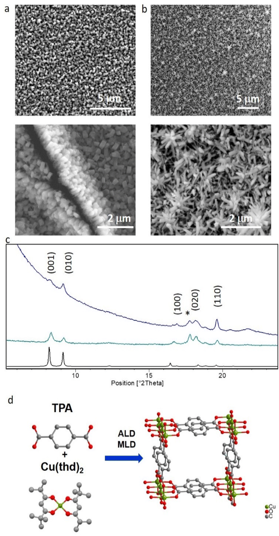 | ||
| Fig. 1 SEM images of the thin film obtained after 160 ALD/MLD cycles on Si (100), lower (top) and higher (bottom) magnifications (a), the film crack in the bottom image shows the oriented growth of the film. SEM images of the thin film obtained after 250 ALD/MLD cycles on Si (100), lower (top) and higher (bottom) magnifications (b). PXRD patterns of the films obtained after 160 cycles (blue) and after 250 cycles (teal), the calculated PXRD diagram for CuTPA (black), * corresponds to the free TPA (c), and the reaction scheme of the ALD/MLD of CuTPA (d). | ||
Structural analysis was performed by means of XRD. The obtained films show good crystallinity as depicted in Fig. 1c. Phase identification clearly demonstrates the formation of a triclinic 3-dimensional CuTPA framework,27 where the copper ions are solely connected by the carboxylate functions and form Cu–O chains that run in the same direction as the one-dimensional pores of ca. 5.2 Å (Fig. 1d). This clarifies the MOF phase obtained from the ALD/MLD process, which differs from the previously assigned paddle-wheel 2-dimensional structure. The observed 3D phase is in accordance with a solventless process, as no other linker than TPA is present in the Cu coordination sphere. The diffractograms in Fig. 1c show some extra Bragg peaks that were attributed to free TPA, probably due to its low volatility that prevents the total removal during the purge step. Attempts to avoid free TPA deposition using a shorter pulse and/or a lower temperature for this precursor (140 °C instead of 180 °C) led to a considerable loss of the film crystallinity that is evidenced by a considerable decrease of the diffraction peak intensity (Fig. S12†). To avoid the presence of unreacted TPA, a 5 μm filter gasket was implemented upstream from the reaction chamber and further studies were conducted with the standard parameters. More importantly, XRD patterns (Fig. 1c) indicate that the film growth starts in an oriented manner, given the large relative intensities of the peaks corresponding to the (010) and (110) inter-reticular planes in the pattern corresponding to 160 cycle grown film. When further ALD/MLD cycles are implemented, the growth orientation becomes more random, as the relative intensities of Bragg peaks are closer to the calculated pattern for CuTPA. This points out that CuTPA growth first preferentially occurs perpendicular to the substrate along the [001] direction of the unit cell, meaning that the pores and the inorganic chains of the MOF run parallel to the substrate (Fig. S10†). After a certain film thickness, the ALD/MLD proceeds more isotropically. This analysis of XRD data corroborated the SEM results (Fig. 1a and b) discussed above. The reproducibility of the 3D phase film growth was checked by performing three times the deposition under the same conditions (Fig. S11†). MOF formation was further confirmed spectroscopically by FTIR analysis.
The spectra (Fig. 3 and Fig. S14†) show vibration bands at 1590 cm−1 and 1390 cm−1 that are assigned to the asymmetric and symmetric vibrations of the carboxylate group, respectively. The Δ between these two frequencies (Δ = 200 cm−1) is characteristic of bidentate bridged carboxylate28 and free TPA displays ν(C![[double bond, length as m-dash]](https://www.rsc.org/images/entities/char_e001.gif) O) and ν(C–O) bands at 1685 cm−1 and 1272 cm−1, respectively (Fig. 3). The obtained values match the ones observed for the bulk CuTPA that was synthesized in solution as a reference for this study (see ESI, Fig. S14a†). It should be noted that the band at 1100 cm−1, visible in the spectrum of CuTPA on Si wafer with native oxide, originates from the substrate (Fig. S14b†) and corresponds to the stretching band of Si–O–Si. The bulk MOF morphology can be described as a near-square shape assembly of platelets (Fig. S5†) while the ALD/MLD grown crystallites display a more elongated parallelepiped shape, indicative of their preferential c-axis orientation.
O) and ν(C–O) bands at 1685 cm−1 and 1272 cm−1, respectively (Fig. 3). The obtained values match the ones observed for the bulk CuTPA that was synthesized in solution as a reference for this study (see ESI, Fig. S14a†). It should be noted that the band at 1100 cm−1, visible in the spectrum of CuTPA on Si wafer with native oxide, originates from the substrate (Fig. S14b†) and corresponds to the stretching band of Si–O–Si. The bulk MOF morphology can be described as a near-square shape assembly of platelets (Fig. S5†) while the ALD/MLD grown crystallites display a more elongated parallelepiped shape, indicative of their preferential c-axis orientation.
To check the adaptability of the process and investigate the impact of the starting surface, the film growth was then performed on crystalline substrates. Sapphire with a a-plane surface orientation and FTO on glass were chosen; both kinds of substrates present oxide/hydroxide functionalities at their surface that are well suited for reacting with the metallic precursor. The ALD/MLD was implemented with the same parameters as for Si (100). The SEM data evidence that a crystalline film is obtained on both substrates, but the crystallite morphology differs (Fig. 2a and b). Indeed, on the sapphire, a rather compact film formed of rod-like crystallites is observed when in the case of FTO, thinner and more dispersed crystallites are deposited. For both films, a good coverage is obtained (Fig. S15c and d†) and Cu and C are detected by EDS (Fig. S18 and S19†). XRD analysis (Fig. 2c) reveals that the same CuTPA phase is clearly formed on the sapphire substrate when in the case of FTO the obtained pattern is ill-defined and does not allow accurate phase identification. This might be due to sparser film coverage. In all cases, FTIR analysis reveals the coordination of copper by the TPA linker (Fig. 3).
 | ||
| Fig. 2 SEM image of the thin film deposited on sapphire, a-oriented substrate (a), SEM image of the thin film deposited on FTO (b), XRD patterns of the films deposited on sapphire (teal) and on FTO (blue); both films were deposited through 250 cycles and the calculated pattern for CuTPA is shown in black (c). | ||
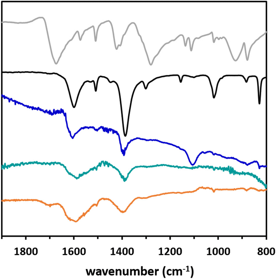 | ||
| Fig. 3 FTIR spectra of TPA (light grey), the bulk CuTPA (black), and CuTPA films grown on Si (100) with native oxide (blue), sapphire (teal) and FTO (orange). | ||
Given the good adaptability of the process, we aimed to explore the heteroepitaxial MOF on MOF growth, using a single crystalline MOF as the substrate. Assembling MOF on MOF heterostructures is of great interest to reach superstructures with tuned mechanical, adsorptive, and photophysical properties.29 To date, core–shell,30–32 layered,33 complex ternary34 and anisotropic35 MOF on MOF superstructures have been reported through solution-based synthesis. To the best of our knowledge, such superstructures have not been reported through the use of the MOF growth in the vapour phase. DMOF-1 (Zn-TPA-DABCO) was chosen as the support because, in its structure, the intermetallic distances are very close to the ones in CuTPA (10.93 and 10.77 Å, respectively, meaning a mismatch of ∼1.5% only, Fig. 4a). Additionally, DMOF-1 is easily obtained as single crystals, offering a molecular material substrate with well-defined planar facets (Fig. 4b and S8†). From single crystal X-Ray diffraction analysis, the crystal orientation was determined, indicating that DMOF-1 grows along its 3 cell axes, with the a axis as the preferential direction (inset Fig. 4b). The pore width of DMOF-1 is insufficient for the diffusion of the Cu(thd)2 precursor; therefore an on-surface only ALD/MLD reaction can be expected. DMOF-1 single crystals were dispersed onto the surface of the Si (100) substrate and the ALD/MLD of CuTPA was performed. From the SEM analysis of the recovered sample, the DMOF-1 surface is clearly altered as it appears covered by nanometric crystallites and a film deposition on the Si wafer is observed (Fig. 4b). This way, a heterostructure resembling a core–shell topology is obtained through ALD/MLD implementation on the MOF surface.
 | ||
| Fig. 4 Representation of the DMOF-1 (up) and CuTPA (bottom) structures and the intermetallic distances (a) and SEM images of DMOF-1 before (top left) and after 250 cycles of ALD/MLD of CuTPA (b). | ||
More importantly, these crystallites are well-oriented perpendicular to the DMOF-1 surface all over the different facets (Fig. 4b and S16†), indicating that the ALD/MLD process allows directional growth on a structured three-dimensional substrate, with comparable intermetallic distances. EDS analysis indicates the presence of both Cu and Zn (Fig. S20†) on the crystal particles. To perform a spatially resolved analysis of the heterostructure, the CuTPA-coated crystals were transferred to an Au grid for Transmission Electron Microscopy (TEM) analysis. The TEM image in Fig. 5a shows thin crystallites sticking out of the DMOF-1 crystal. Elemental mapping was performed in STEM-EDS mode (Fig. 5b and c), and the results clearly show that a Cu containing material is deposited on top of the Zn-based solid, demonstrating for the first time that a heterostructure is accessible using ALD/MLD on a MOF surface. In this set up, the deposition occurs both on the Si (100) and on DMOF-1 surfaces, which prevents thorough structural analysis of the heterostructure by X-Ray diffraction; nonetheless the obtained pattern displays Bragg peaks corresponding to the CuTPA phase (Fig. S13†).
 | ||
| Fig. 5 TEM image of DMOF-1 after 250 cycles of ALD/MLD of CuTPA (a), STEM image (b) and the corresponding elemental mapping performed by STEM-EDS (c). | ||
4. Conclusions
In summary, this study clarifies and expands the scope of the ALD/MLD growth of crystalline MOF thin films. In particular, we demonstrate that the 3D CuTPA MOF films can be easily obtained through the vapour phase layer by layer growth and that this process is adaptable to different kinds of amorphous (Si with native oxide) or crystalline (sapphire, FTO) inorganic substrates. Importantly, for the first time an oriented MOF growth in the vapour phase is detected and the orientation of the crystallites is determined. Notably, the directional MOF growth is also observed on the facets of DMOF-1 single crystals leading to an unprecedented core–shell material by vapour phase synthesis. This proves the ability of the ALD/MLD technique to accomplish heteroepitaxial growth on structured hybrid materials with lattice matching topologies. Our results indicate that the ALD/MLD deserves further and wider advancement for the processing of hybrid materials and the development of functional heterojunctions.Author contributions
Ben Gikonyo: investigation and validation; Fangbing Liu: investigation and validation; Siddhartha De: investigation; Catherine Journet: resources, data curation, and visualization; Catherine Marichy: conceptualization, project administration, supervision, visualization, writing – original draft, and writing – review & editing; Alexandra Fateeva: conceptualization, funding acquisition, resources, project administration, supervision, visualization, writing – original draft, and writing – review & editing.Conflicts of interest
The authors declare that they have no competing financial interests or personal relationships that could have appeared to influence the work reported in this paper.Acknowledgements
The authors gratefully acknowledge Pr. Jacques Jose for the technical help, the Centre Technologique des Microstructures of the University of Lyon for providing the electron microscopy facilities, the French Ministry of National Education, Research and Technology, the University Lyon 1 and the CNRS for financial support; this work was supported by the French National Research Agency grant (ANR-17-CE09-0029-01).References
- J. Plutnar and M. Pumera, Applications of Atomic Layer Deposition in Design of Systems for Energy Conversion, Small, 2021, 17(39), 2102088, DOI:10.1002/smll.202102088.
- T. Tripathi and M. Karppinen, Atomic Layer Deposition of P-Type Semiconducting Thin Films: A Review, Adv. Mater. Interfaces, 2017, 4(24), 1700300, DOI:10.1002/admi.201700300.
- Y. Zhao, L. Zhang, J. Liu, K. Adair, F. Zhao, Y. Sun, T. Wu, X. Bi, K. Amine, J. Lu and X. Sun, Atomic/Molecular Layer Deposition for Energy Storage and Conversion, Chem. Soc. Rev., 2021, 50(6), 3889–3956, 10.1039/d0cs00156b.
- M. Leskelä, M. Mattinen and M. Ritala, Review Article: Atomic Layer Deposition of Optoelectronic Materials, J. Vac. Sci. Technol., B: Nanotechnol. Microelectron.: Mater., Process., Meas., Phenom., 2019, 37(3), 030801, DOI:10.1116/1.5083692.
- R. W. Johnson, A. Hultqvist and S. F. Bent, A Brief Review of Atomic Layer Deposition: From Fundamentals to Applications, Mater. Today, 2014, 17(5), 236–246, DOI:10.1016/j.mattod.2014.04.026.
- S. M. George, Atomic Layer Deposition: An Overview, Chem. Rev., 2010, 110(1), 111–131, DOI:10.1021/cr900056b.
- T. Yoshimura, S. Tatsuura and W. Sotoyama, Polymer Films Formed with Monolayer Growth Steps by Molecular Layer Deposition, Appl. Phys. Lett., 1991, 59(4), 482–484, DOI:10.1063/1.105415.
- A. A. Dameron, D. Seghete, B. B. Burton, S. D. Davidson, A. S. Cavanagh, J. A. Bertrand and S. M. George, Molecular Layer Deposition of Alucone Polymer Films Using Trimethylaluminum and Ethylene Glycol, Chem. Mater., 2008, 20(10), 3315–3326, DOI:10.1021/cm7032977.
- K. B. Klepper, O. Nilsen and H. Fjellvåg, Deposition of Thin Films of Organic–Inorganic Hybrid Materials Based on Aromatic Carboxylic Acids by Atomic Layer Deposition, Dalton Trans., 2010, 39(48), 11628–11635, 10.1039/C0DT00817F.
- E. Ahvenniemi and M. Karppinen, Atomic/Molecular Layer Deposition: A Direct Gas-Phase Route to Crystalline Metal–Organic Framework Thin Films, Chem. Commun., 2016, 52(6), 1139–1142, 10.1039/C5CC08538A.
- E. Ahvenniemi and M. Karppinen, In Situ Atomic/Molecular Layer-by-Layer Deposition of Inorganic–Organic Coordination Network Thin Films from Gaseous Precursors, Chem. Mater., 2016, 28(17), 6260–6265, DOI:10.1021/acs.chemmater.6b02496.
- J. Heiska, O. Sorsa, T. Kallio and M. Karppinen, Benzenedisulfonic Acid as an ALD/MLD Building Block for Crystalline Metal-Organic Thin Films, Chem. – Eur. J., 2021, 27(34), 8799–8803, DOI:10.1002/chem.202100538.
- J. Multia, J. Heiska, A. Khayyami and M. Karppinen, Electrochemically Active In Situ Crystalline Lithium-Organic Thin Films by ALD/MLD, ACS Appl. Mater. Interfaces, 2020, 12(37), 41557–41566, DOI:10.1021/acsami.0c11822.
- J. Penttinen, M. Nisula and M. Karppinen, Atomic/Molecular Layer Deposition of s-Block Metal Carboxylate Coordination Network Thin Films, Chem. – Eur. J., 2017, 23(72), 18225–18231, DOI:10.1002/chem.201703704.
- A. Tanskanen and M. Karppinen, Iron-Terephthalate Coordination Network Thin Films Through In situ Atomic/Molecular Layer Deposition, Sci. Rep., 2018, 8, 8976, DOI:10.1038/s41598-018-27124-7.
- J. Heiska, M. Nisula, E.-L. Rautama, A. J. Karttunen and M. Karppinen, Atomic/Molecular Layer Deposition and Electrochemical Performance of Dilithium 2-Aminoterephthalate, Dalton Trans., 2020, 49(5), 1591–1599, 10.1039/C9DT04572D.
- K. B. Lausund, V. Petrovic and O. Nilsen, All-Gas-Phase Synthesis of Amino-Functionalized UiO-66 Thin Films, Dalton Trans., 2017, 46(48), 16983–16992, 10.1039/C7DT03518G.
- K. B. Lausund and O. Nilsen, All-Gas-Phase Synthesis of UiO-66 through Modulated Atomic Layer Deposition, Nat. Commun., 2016, 7(1), 13578, DOI:10.1038/ncomms13578.
- L. D. Salmi, M. J. Heikkilä, E. Puukilainen, T. Sajavaara, D. Grosso and M. Ritala, Studies on Atomic Layer Deposition of MOF-5 Thin Films, Microporous Mesoporous Mater., 2013, 182, 147–154, DOI:10.1016/j.micromeso.2013.08.024.
- L. D. Salmi, M. J. Heikkilä, M. Vehkamäki, E. Puukilainen, M. Ritala and T. Sajavaara, Studies on Atomic Layer Deposition of IRMOF-8 Thin Films, J. Vac. Sci. Technol., A, 2015, 33(1), 01A121, DOI:10.1116/1.4901455.
- K. B. Lausund, M. S. Olsen, P.-A. Hansen, H. Valen and O. Nilsen, MOF Thin Films with Bi-Aromatic Linkers Grown by Molecular Layer Deposition, J. Mater. Chem. A, 2020, 8(5), 2539–2548, 10.1039/C9TA09303F.
- I. Stassen, D. De Vos and R. Ameloot, Vapor-Phase Deposition and Modification of Metal–Organic Frameworks: State-of-the-Art and Future Directions, Chem. – Eur. J., 2016, 22(41), 14452–14460, DOI:10.1002/chem.201601921.
- P. Su, M. Tu, R. Ameloot and W. Li, Vapor-Phase Processing of Metal–Organic Frameworks, Acc. Chem. Res., 2022, 55(2), 186–196, DOI:10.1021/acs.accounts.1c00600.
- C. Crivello, S. Sevim, O. Graniel, C. Franco, S. Pané, J. Puigmartí-Luis and D. Muñoz-Rojas, Advanced Technologies for the Fabrication of MOF Thin Films, Mater. Horiz., 2021, 8(1), 168–178, 10.1039/D0MH00898B.
- M. Sánchez-Sánchez, N. Getachew, K. Díaz, M. Díaz-García, Y. Chebude and I. Díaz, Synthesis of Metal–Organic Frameworks in Water at Room Temperature: Salts as Linker Sources, Green Chem., 2015, 17(3), 1500–1509, 10.1039/C4GC01861C.
- J. Ma, A. P. Kalenak, A. G. Wong-Foy and A. J. Matzger, Rapid Guest Exchange and Ultra-Low Surface Tension Solvents Optimize Metal–Organic Framework Activation, Angew. Chem., Int. Ed., 2017, 56(46), 14618–14621, DOI:10.1002/anie.201709187.
- C. G. Carson, G. Brunnello, S. G. Lee, S. S. Jang, R. A. Gerhardt and R. Tannenbaum, Structure Solution from Powder Diffraction of Copper 1,4-Benzenedicarboxylate, Eur. J. Inorg. Chem., 2014, 2014(12), 2140–2145, DOI:10.1002/ejic.201301543.
- K. Tan, N. Nijem, P. Canepa, Q. Gong, J. Li, T. Thonhauser and Y. J. Chabal, Stability and Hydrolyzation of Metal Organic Frameworks with Paddle-Wheel SBUs upon Hydration, Chem. Mater., 2012, 24(16), 3153–3167, DOI:10.1021/cm301427w.
- R. Haldar and C. Wöll, Hierarchical Assemblies of Molecular Frameworks—MOF-on-MOF Epitaxial Heterostructures, Nano Res., 2021, 14(2), 355–368, DOI:10.1007/s12274-020-2953-z.
- S. Furukawa, K. Hirai, K. Nakagawa, Y. Takashima, R. Matsuda, T. Tsuruoka, M. Kondo, R. Haruki, D. Tanaka, H. Sakamoto, S. Shimomura, O. Sakata and S. Kitagawa, Heterogeneously Hybridized Porous Coordination Polymer Crystals: Fabrication of Heterometallic Core–Shell Single Crystals with an In-Plane Rotational Epitaxial Relationship, Angew. Chem., Int. Ed., 2009, 48(10), 1766–1770, DOI:10.1002/anie.200804836.
- M. Faustini, J. Kim, G.-Y. Jeong, J. Y. Kim, H. R. Moon, W.-S. Ahn and D.-P. Kim, Microfluidic Approach toward Continuous and Ultrafast Synthesis of Metal–Organic Framework Crystals and Hetero Structures in Confined Microdroplets, J. Am. Chem. Soc., 2013, 135(39), 14619–14626, DOI:10.1021/ja4039642.
- D. Yu, Q. Song, J. Cui, H. Zheng, Y. Zhang, J. Liu, J. Lv, T. Xu and Y. Wu, Designing Core–Shell Metal–Organic Framework Hybrids: Toward High-Efficiency Electrochemical Potassium Storage, J. Mater. Chem. A, 2021, 9(46), 26181–26188, 10.1039/D1TA08215A.
- K. Ikigaki, K. Okada, Y. Tokudome, T. Toyao, P. Falcaro, C. J. Doonan and M. Takahashi, MOF-on-MOF: Oriented Growth of Multiple Layered Thin Films of Metal–Organic Frameworks, Angew. Chem., Int. Ed., 2019, 58(21), 6886–6890, DOI:10.1002/anie.201901707.
- C. Liu, Q. Sun, L. Lin, J. Wang, C. Zhang, C. Xia, T. Bao, J. Wan, R. Huang, J. Zou and C. Yu, Ternary MOF-on-MOF Heterostructures with Controllable Architectural and Compositional Complexity via Multiple Selective Assembly, Nat. Commun., 2020, 11(1), 4971, DOI:10.1038/s41467-020-18776-z.
- G. Lee, S. Lee, S. Oh, D. Kim and M. Oh, Tip-To-Middle Anisotropic MOF-On-MOF Growth with a Structural Adjustment, J. Am. Chem. Soc., 2020, 142(6), 3042–3049, DOI:10.1021/jacs.9b12193.
Footnote |
| † Electronic supplementary information (ESI) available. See DOI: https://doi.org/10.1039/d2dt03216c |
| This journal is © The Royal Society of Chemistry 2023 |