
 Open Access Article
 This Open Access Article is licensed under a Creative Commons Attribution-Non Commercial 3.0 Unported Licence
Diagnosis of doped conjugated polymer films using hyperspectral imaging
Vijila
Chellappan
 *a,
Adithya
Kumar
a,
Saif
Ali khan
a,
Pawan
Kumar
a and
Kedar
Hippalgaonkar
*ab
*a,
Adithya
Kumar
a,
Saif
Ali khan
a,
Pawan
Kumar
a and
Kedar
Hippalgaonkar
*ab
aInstitute of Materials Research and Engineering, Agency for Science Technology and Research, #08-03, 2 Fusionopolis Way, Innovis, Singapore 138634, Singapore. E-mail: c-vijila@imre.a-star.edu.sg
bMaterials Science and Engineering, Nanyang Technological University, 50 Nanyang Avenue, Singapore 639798, Singapore. E-mail: kedar@ntu.edu.sg
First published on 10th February 2023
Abstract
Absorption spectra of doped conjugated polymer films provide valuable information on the degree of crystallinity, doping efficiency, material composition, and film thickness. The absorption spectral features commonly observed in doped polymers are due to intra-, inter-chain excitons, exciton–phonon coupling, polarons, and bipolarons that are branched differently in films prepared at different process parameters and doping conditions. Thus, the spectral features of thin films can be used to monitor and tune process parameters. However, probing spectral information at a point does not provide complete information on the solution-processed films where film characteristics are significantly influenced by uncontrolled process parameters. Hyperspectral imaging (HSI) is a high throughput spectral diagnostic method that provides the spatial distribution of spectral features where the process-induced variations of thin film quality and their influence on final performance metrics can be effectively analysed. In this report, we present a methodology for diagnosing thin film characteristics using the HSI technique by implementing automated spectral feature extraction and visualisation. For this study, we used the well-established F4TCNQ-doped regio regular poly-3-hexyl thiophene (P3HT) film as a model system and show film quality parameters, such as variation in film thickness, homogeneity of materials composition, degree of crystallinity and polaron concentration. We also present a generic process flow for the rapid screening of thin film and process optimization using the HSI technique.
Introduction
In recent years, doped conjugated polymers are attracting significant research interest due to their advantage of tunable electronic properties and ability to manufacture large-area flexible devices using cost-efficient methods such as roll-to-roll coating, drop casting, or blade coating techniques.1–4 In particular, molecular doping of conjugated polymers using solution-processable methods is highly suitable for flexible electronic applications including organic thermoelectric and sensor devices.5–7 To realise practical devices based on doped conjugated polymers, the electrical conductivity needs to be significantly increased.8 The electrical conductivity of doped conjugated polymers can be as large as ∼103 S cm−1,9,10 however, these high-performing polymers have poor environmental stability and processability.11 As a result, significant efforts have been dedicated to developing conjugated polymers with different side chains to improve the solubility and backbone modification for tuning the planarity and inter-chain stacking.12–15 Among various conjugated polymer families, polythiophene derivatives show the most promising optical and electrical characteristics where the electrical conductivity is significantly improved through structural modifications, doping strategies, and by controlling the microstructure through process optimization.16–21The electrical conductivity of the most commonly used poly(3-hexylthiophene-2,5-diyl) (P3HT) doped with 2,3,5,6-tetrafluoro-7,7,8,8-tetracyanoquinodimethane (F4TCNQ) is around 10 S cm−1,22 which increases to 100 S cm−1 when the P3HT structure is modified with ethylene glycol side chains.23 Another prototypical conjugated polymer poly(bisdodecylquaterthiophene) (PQT) shows the highest electrical conductivity of 350 S cm−1 after introducing sulphur atoms into side chains and upon doping with NOBF4.24 The alteration of energy levels due to chemical structure modification facilitates integer charge transfer between the polymer and dopants,21,25 where the microstructure of the doped polymer film plays a dominant role in controlling electrical conductivity. The modification of sidechains with certain atoms promotes the interaction between the side chains and dopant molecules, thus increasing the lamellar distance while closely packing the polymer backbone and promotes charge transport along the π–π stacking direction.
In general, the electrical conductivity of solution processable-doped conjugated polymeric films depends on various inter-related process parameters such as film preparation method, process solvents, surface treatments, doping method, and dopant concentration.26,27 All these inter-related process variations cause significantly different films where morphological variations, different degrees of aggregation, inhomogeneous doping, non-uniformity, and un-intentional defects, which affect the performance of the final devices. The optical absorption spectra have different spectral signatures that are sensitive to structural and morphological variations and these spectral fingerprints can be tracked to optimize process conditions for high-performance thin films.28–30 However, the spectral fingerprints from a single point measurement do not provide the actual representation of the film characteristics. The optical and electrical properties of the doped films are significantly influenced by local structural characteristics. However, the effect of the local domain on material properties is not commonly investigated. Maddali et al. studied the local electrical properties in amorphous and crystalline domains of electrochemically-doped P3HT films using conductive AFM measurements.31 It has been shown that crystalline domains have a high degree of doping compared to amorphous domains, resulting in superior local electrical conductivity.26 This indicates that the possibility of maximizing the crystalline domains increases the doping efficiency and the resultant electrical conductivity of the film. Mapping localized thin film characteristics with non-destructive methodologies can accelerate the optimization and materials identification process for maximising the performance level.
Spatially resolved spectroscopic techniques or hyperspectral imaging allow non-destructive chemical and morphology mapping of materials. Available information from hyperspectral imaging techniques depends on the spectral range, detector type, measurement mode, and the type of excitation source.32 Infrared (IR) imaging and Raman imaging techniques are the most used methods to map vibrational frequencies of different chemical bonds for identifying specific material constituents.33,34 To enable spectral imaging on a wide variety of materials with varying degrees of spectral and spatial resolution, different instrumental configurations are developed. For example, microattenuated total reflection Fourier transform infrared (ATR-FTIR) spectroscopic imaging is used for visualising molecular orientation in polymeric spherulites.35 Confocal Raman microscopy is used to map the charge carrier distribution in carbon nanotube-based transistor devices.34 Spatially localised chemical information of powder samples at the nanoscale is studied by secondary electron hyperspectral imaging (SEHI).36 Although these advanced techniques provide localised chemical, morphological and molecular information with higher spatial resolution, it requires complex instrumentation and tedious experimental/data analysis methodologies due to multiple overlapping peaks and weak signal strengths. Visible range hyperspectral imaging is a relatively simple technique that measures the broad absorption spectral features due to electronic transitions.
The hyperspectral imaging technique is generally used for remote sensing applications, monitoring plant health by predicting the onset of diseases and stress,37 evaluating the quality attributes of meat,38,39 and predicting internal quality and moisture content in fruits.40 In recent years, the HSI technique has gained popularity as a non-destructive, fast-quality assessment method for a wide range of applications. Randeberg et al.41 reported real-time optical diagnostics of the skin using hyperspectral imaging by developing an algorithm for extracting skin parameters. Near-infrared HSI has been widely used as a non-destructive analytical tool for biological materials.42 Different modes of HSI, such as Raman HSI, photoluminescence HSI, combined with signal enhancement strategies are used to study various types of nanomaterials where the high spectral and spatial resolution of HSI technique enables the simultaneous measurement of nanoparticle distribution and its material properties.43–45
In this study, we use the hyperspectral imaging (HSI) technique in the visible spectral region for simultaneous probing of spectral and spatial characteristics of the doped conjugated polymer films with a spatial resolution of 120 μm. The pictorial representation of the hyperspectral imaging system, model hypercube, and spectral features for amorphous, semi-crystalline, and doped conjugated polymeric films are shown in Fig. 1(a), (b), and (c) respectively. The spectra shown in Fig. 1(c) is for illustrative purpose based on the peak shift observed in most of the conjugated polymers at the amorphous, semi-crystalline, and doped state.46,47 It is well known that the absorption spectrum of fully dissolved pristine-conjugated polymer shows a broad spectrum with a single peak corresponding to intrachain π–π* transition. With the increase of aggregation or planarity, the intrachain π–π* transition shows a red spectral shift compared to the amorphous phase with additional spectral features corresponding to inter-band transitions. When the film is doped, two sub-band-gap spectral features appear at the low-energy spectral region in addition to the suppression of high-energy features corresponding to neutral excitons due to π–π* transition.48 The total suppression of absorption due to neutral excitons is an indication of complete oxidation/reduction or doping. The films prepared by solution methods show mixed domains on the same film corresponding to un-doped regions, partially doped, and fully doped regions if the process conditions are not optimised, or there are process-related immiscibility issues. Hyperspectral imaging on these films is extremely useful for identifying these localised domains by probing the spectral features. We show how the use of automated analysis of an HSI cube with visualisation of spectral feature distribution can be used as a fast-screening method to identify suitable films for device fabrication or optimizing the process conditions for desired film morphology. The device performance indicators, such as efficiency and lifetime strongly depend on the film quality, thus fast HSI screening of films with visualisation of representative parameters eliminates the requirement of the tedious process involved in device fabrication and complex characterisation studies that can be carried out with selected high-quality films.
 | ||
| Fig. 1 (a) Pictorial representation of hyperspectral imaging system, (b) hypercube with spatial and spectral information, and (c) model spectral features corresponding to amorphous, semi-crystalline, and doped films, respectively. Three key spectral features can be observed from the spectra: the spectral shift to the red region, the presence of vibronic shoulders, and suppression of absorption due to neutral excitons. | ||
The prototypical conjugated polymer: regio-regular poly-3 hexyl thiophene (RR-P3HT) films prepared by five different solvents is used for this work as the microstructure of the RR-P3HT film is sensitive to process solvents that creates different microstructures of varying crystallinity. The P3HT films are doped with F4TCNQ using the sequential doping method and the concentration of F4TCNQ in nitromethane is varied from 1 mM to 30 mM. The difference in the film microstructure influences the doping efficiency in addition to the distribution of dopants within the film. The hyperspectral image cube is composed of thousands of spatial pixels with more than 250 spectral channels for each pixel, thus the image file is large and multidimensional as every pixel provides complete spectral information or chemical fingerprint of the materials. The analysis of hypercube requires specific software to extract the spectral features. In this work, we implemented automated hyperspectral image cube analysis using python packages to map the spectral features corresponding to uniformity, homogeneity, and the formation of polarons.
Experimental
Materials
Electronics grade regioregular P3HT flakes and F4TCNQ were obtained from Reike Metals and Sigma-Aldrich respectively. Both P3HT and F4TCNQ were stored in the glove box, where we did the weighing and solution preparation. The P3HT concentration of 10 mg ml−1 was prepared using different process solvents (chlorobenzene, chloroform, tetrahydrofuran, toluene, and xylene) to obtain thin films with different microstructures. The F4TCNQ was dissolved in nitromethane by varying the concentration from 1 mM to 30 mM. The films were prepared on a 2.5 cm × 2.5 cm quartz substrate. The substrates were cleaned using acetone and IPA solution and subsequently underwent ultra-sonification for 10 minutes. The substrates were dried and treated with ozone at a temperature of 100 °C for 10 minutes. The films were prepared by spin coating (spin speed: 1000 rpm and time 90 s) and annealed on a hot plate at a temperature of 100 °C for 5 minutes. The annealed films were dipped into an F4TCNQ solution of varying concentrations. We prepared 5 pristine films prepared with five different process solvents and 30-doped films of varying dopant concentrations and process solvents. The pristine and doped films were characterised on the same day to avoid the effects of degradation and de-doping. The measurement sequence was the hyperspectral image of the films, four-point probe, UV-Vis-NIR followed by surface profilometry for thickness measurement. The measurement details are elaborated in the following section.Hyperspectral image acquisition
We used a hyperspectral-imaging system from Resonon, USA (model: PIKA-L) in this study. The hyperspectral imaging system has a spectral range from 400 nm to 1000 nm with a spectral and spatial resolution of 2.1 nm and ∼120 μm, respectively. In this configuration, the broadband halogen light is dispersed via a rod lens for line light illumination. The rod lens is mounted under a transparent sample stage for the transmittance configuration. The sample holder is attached with a linear translational stage where the single spatial line is collected at a time (push-broom technique or line scan) by the 2D array detector. The axis corresponding to the spatial line forms one of the dimensions of the 2D sensor and the other dimension corresponds to the spectral axis of the sensor as shown in Fig. 1(b). While scanning across the sample, multiple 2D arrays are collected and these 2D arrays are stacked together to form a 3D image cube. The imaging conditions were set at the frame rate of 75 Hz, integration time of 11.5 ms, horizontal field width of 9 cm, and scanning speed of 0.8 cm s−1.The acquisition of hyperspectral images involves three major steps such as (1) dark correction, (2) reference correction, and (3) sample image acquisition. The dark correction was carried out by recording the camera response (D) without light illumination and the reference correction was carried out by recording the response of the HSI system and light source with the reference substrate (quartz). The intensity of the light passing through the reference substrate (I0) and the sample (I) for every pixel was measured and the transmittance (T) of the sample was calculated according to the relation given below:
 | (1) |
The recorded hyperspectral image cube provides the transmittance of the sample that includes automatic correction of both, the dark and reference. The response correction was carried out with reference substrates covering the entire line light illumination length that removes the inhomogeneity of the rod lens and the intensity variation of the light source. The transmittance spectrum is converted into absorbance (A) using the equation as shown below:
| A = −log(T) | (2) |
The image cube is in a band interleaved by line (.bil) format accompanied by a header file (bil.hdr) containing the nature of the image. The HSI cubes were analysed using Python in Jupyter notebook to extract the spectral features of each pixel. The size of the image analysed for feature visualisation was 2 cm × 2 cm.
Four-point probe measurement
The sheet resistance of the doped films was measured using a semi-automated four-point probe (4pp) measurement setup. The current–voltage characteristics were measured using a Keithley 2450 source meter in a four-point probe configuration. The geometry factor of 3.8 was multiplied by the slope obtained from the I–V curve and the conductivity (σ, S cm−1) of the film was calculated using the following equation: | (3) |
Results and discussion
The RGB image of the pristine P3HT films prepared with five different process solvents is shown in Fig. 2(a). The thickness variation due to colour change, defects, and scratches in the films are visible with the RGB image, however, the spectral fingerprints of every pixel carry more information on the microstructure and material composition on the selected domains. The basic absorption spectral characteristics, such as maximum absorbance (Amax) and peak energy (Emax) were extracted by automated HSI analysis of the data cube and the spatial mapping of the features are shown in Fig. 2(b) and (c), respectively. The peak absorbance map indicates the dispersion of the absorbance across the pixels, which is useful to estimate the thickness uniformity within the film and the thickness variation between the films due to process solvents. The narrow distribution of absorbance within the film is an indication of better film uniformity. The film prepared from THF is thicker than the other films and xylene produced more uniform thin films as the absorbance distribution was narrower than the other films. The peak energy map (Fig. 2(c)) shows the variation in microstructure such as the semi-crystalline phase (aggregated) or amorphous phase. The light blue colour (corresponding to the peak energy of ∼2.25 eV) coded region indicates aggregated domains and the pink colour coded region indicates the amorphous region (corresponding to the peak energy of ∼2.5 eV) based on P3HT spectral fingerprints. It is well known that the absorption spectra shift towards low energy for the aggregated region than the coiled confirmation or the amorphous region. It can be easily seen that the film prepared with xylene produces more light blue coloured domains, whereas, the film prepared from THF shows mainly pink-coloured domains, indicating that the films prepared by xylene have a high degree of aggregation than the other films and THF produces an amorphous film. The results indicate that the process solvent variation produces very different film characteristics although all other process parameters (concentration, spin speed, annealing temperature) remained constant except the solvent. It is well established that the process solvents/conditions significantly affect the microstructure/degree of crystallinity.49,50 | ||
| Fig. 2 (a) Absorption spectral map of pristine P3HT films in different solvents. (b) Average absorbance spectra, and (c) average free exciton width estimated from the absorption ratio between A0–0, and A0–1 as shown in eqn (4). | ||
The degree of crystallinity is governed by various factors such as planarization, polymer chain entanglement, nature of orientation, and inter/intra-chain interaction. Simple absorption spectroscopy can provide information on inter and intra-chain interaction, exciton–phonon coupling, and the fraction of film made up of the aggregates. The absorption spectral features of the polymeric thin films mainly arise from electronic interactions along the polymer chain (J-aggregates or intrachain interaction), between the polymeric chains (H-aggregates), and the combination of both J and H aggregates. The coupling of electronic and vibrational transition creates spectral splitting and the absorption intensity ratio between the inter-chain absorption and intra-chain absorption provides the degree of crystallinity and the degree of excitonic coupling within the aggregate. Therefore the absorption spectral splitting is used as an indicator of coupling between the electronic and vibrational degrees of freedom.51,52
The absorption spectra of regio-regular P3HT film are explained using an analytical form of weakly interacting H-aggregate model where the free exciton bandwidth is related to the absorption ratio between the inter-chain and intra-chain interaction, as shown in eqn (4)49,53–55
 | (4) |
![[double bond, length as m-dash]](https://www.rsc.org/images/entities/char_e001.gif) C symmetric stretch with energy 0.18 eV, and assuming Huang–Rhys factor of 1. eqn (4) is valid for the weak exciton-coupling limit where the Coulomb coupling is restricted to the nearest neighbour.56 The average absorption spectra extracted from the HSI of the films are shown in Fig. 2(b) where the spectral features due to inter-chain interaction and intra-chain interactions are indicated as A0–0 and A0–1, respectively. The absorption ratio (A0–0/A0–1) < 1 is an indication of dominant H-aggregates in the system, whereas a ratio greater than 1 is an indication of J-aggregation.57 The ratio of spin-coated P3HT films reported is in the range of 0.65 to 0.9, which is consistent with our results. The ratio (A0–0/A0–1) > 1 is generally observed for P3HT nanofibers where increasing the planarity of the polymer chains promotes intra-chain exciton coupling and dominates over inter-chain exciton coupling.57 The free exciton bandwidth is calculated using experimentally-measured absorption ratio from each pixel of the HSI data cube using relation (4) and the dispersion of free exciton width across the pixels is shown in Fig. 2(c). The average values of ‘W’ extracted from HSI are shown in Fig. 2(c) and the obtained values are consistent with reported values.53 The films prepared from THF show the highest ‘W’ in the range of 150 meV, whereas the films prepared from xylene show ‘W’ below 100 meV, which is also sensitive to the aging of the film. Hynynen et al.17 investigated the correlation between the exciton bandwidth and electrical conductivity, where the electrical conductivity systematically increased with the decrease of free exciton bandwidth. It has also been demonstrated that the films with smaller ‘W’ exhibit better charge mobility and device performance due to favourable microstructure for charge transport.49
C symmetric stretch with energy 0.18 eV, and assuming Huang–Rhys factor of 1. eqn (4) is valid for the weak exciton-coupling limit where the Coulomb coupling is restricted to the nearest neighbour.56 The average absorption spectra extracted from the HSI of the films are shown in Fig. 2(b) where the spectral features due to inter-chain interaction and intra-chain interactions are indicated as A0–0 and A0–1, respectively. The absorption ratio (A0–0/A0–1) < 1 is an indication of dominant H-aggregates in the system, whereas a ratio greater than 1 is an indication of J-aggregation.57 The ratio of spin-coated P3HT films reported is in the range of 0.65 to 0.9, which is consistent with our results. The ratio (A0–0/A0–1) > 1 is generally observed for P3HT nanofibers where increasing the planarity of the polymer chains promotes intra-chain exciton coupling and dominates over inter-chain exciton coupling.57 The free exciton bandwidth is calculated using experimentally-measured absorption ratio from each pixel of the HSI data cube using relation (4) and the dispersion of free exciton width across the pixels is shown in Fig. 2(c). The average values of ‘W’ extracted from HSI are shown in Fig. 2(c) and the obtained values are consistent with reported values.53 The films prepared from THF show the highest ‘W’ in the range of 150 meV, whereas the films prepared from xylene show ‘W’ below 100 meV, which is also sensitive to the aging of the film. Hynynen et al.17 investigated the correlation between the exciton bandwidth and electrical conductivity, where the electrical conductivity systematically increased with the decrease of free exciton bandwidth. It has also been demonstrated that the films with smaller ‘W’ exhibit better charge mobility and device performance due to favourable microstructure for charge transport.49
The P3HT films prepared using different process solvents were doped with F4TCNQ by the sequential doping method. The films were immersed in F4TCNQ/nitromethane solution of different concentrations varying from 1 mM to 30 mM. The efficiency of doping and the process-induced defects on film characteristics were analysed using HSI with automated data analysis and visualisation of spatial maps of spectral features. The average absorption spectra of the F4TCNQ-doped P3HT film extracted from an HSI cube are shown in Fig. 3(a) where the spectral fingerprints due to neutral excitons (π–π*), high-energy polarons (P2) are marked in the spectra and the associated electronic transitions are indicated in the inset of Fig. 3(a). Our HSI system can only probe neutral excitons (π–π*), and high-energy polarons (P2), the low-energy polarons (P1) cannot be probed due to limited spectral range. Generally, the absorption spectra of the aggregated P3HT film show characteristics peaks at around 2.05 eV, 2.25 eV, and 2.35 eV attributed to neutral excitons coupled with vibronic transitions.58 Doping introduces two additional sub-bandgap transitions at ∼1.3–1.6 eV, and ∼0.5 eV due to high energy polarons (P2) and (P1) transitions, respectively, where the P2 peak is overlapped with F4TCNQ anions.59 Wang et al. further deconvoluted the 1.3–1.6 eV spectral features into high-energy polarons, charged anions, low-energy polarons, and bipolarons.48
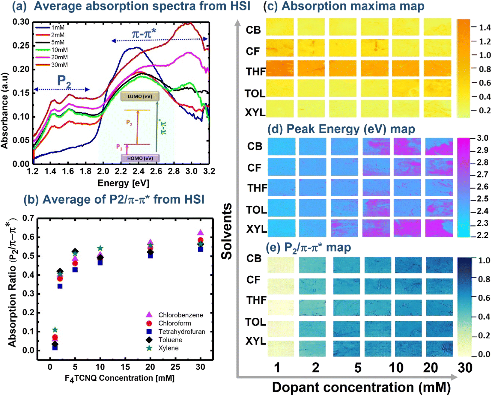 | ||
| Fig. 3 (a) Absorption spectrum of F4TCNQ doped P3HT film extracted from HSI showing the spectral features corresponding to π–π* transition (neutral exciton) of P3HT and F4TCNQ, high-energy polaron (P2) and the corresponding energy level diagram is shown in the inset of (a); (b) average value of the absorption ratio between P2 and π–π* transition (P3HT) extracted from HSI; (c) mapping of absorption maxima and (d) the corresponding energy showing the film uniformity and homogeneity of doped films, respectively; (e) mapping of absorption ratio showing the efficiency of polaron generation. A higher absorption ratio indicates a better generation yield of polarons. The absorption ratio less than unity is shown in (b) and (e) suggesting incomplete doping. | ||
The average absorption spectra extracted from the hyperspectral image of doped P3HT films prepared from xylene are shown in Fig. 3(a), which shows all the spectral features of F4TCNQ-doped P3HT films and the peak energy is consistent with the literature values.48,59 It can be seen that in the spectra at higher dopant concentrations (10–30 mM), there is a strong feature at ∼3.2 eV due to neutral F4TCNQ. The spectra also indicated that all the films used in this study were incompletely doped, as features corresponding to the π–π* transition of neutral P3HT, singly charged polarons, and the F4TCNQ anions were seen and no complete bleaching of absorption due to neutral excitons was observed. The absorption maxima of all the pixel spectra are extracted and the visualisation of the dispersion of the absorption intensity across the pixels and the corresponding peak energy map is shown in Fig. 3(c) and (d). The absorption intensity is directly related to the film thickness and the thickness variation due to the process solvent and the influence of film thickness due to the doping process can be easily visualised in this map. It has been shown that film thickness plays a critical role in the doping process and electrical conductivity optimization.20 It can be seen that the films prepared from THF solution always result in thicker films compared to the films prepared from other solvents. The films prepared from chlorobenzene and xylene produce thinner and more uniform films. The film thickness and morphology vary significantly with polymer solubility, surface treatment of a substrate, solvent evaporation rate, and spin conditions.60–63 The absorption maxima wavelength (peak energy) was also extracted as shown in Fig. 3(d). The peak energy map provides information on film homogeneity and uniformity of doping as the doped and un-doped films have distinctly different spectral fingerprints. The peak energy of the film with low dopant concentration is around 2.3 eV, which is attributed to the absorption of pristine P3HT. If the films are fully doped, the absorption due to π–π* transition vanishes, thus the peak energy should shift to low energy region where completely oxidised films show dominant absorption due to polarons. A significant portion of highly doped films (10 mM, 20 mM and 30 mM) show peak energy > 3 eV (pink coloured regions). The absorption energy of neutral F4TCNQ molecule is ∼3 eV, thus the pink region indicates the deposition or aggregation of F4TCNQ showing film inhomogeneity and non-uniform doping.
To analyse the efficiency of doping, the absorption ratio (P2/π–π*) between the polarons and neutral excitons is commonly used, as the absorption ratio is directly proportional to the polaron concentration. The rate of change of absorption ratio with the dopant concentration provides information on doping efficiency and the optimum level of dopant concentration. In this study, the absorption of high-energy polaron (P2) at 1.5 eV and neutral exciton ∼2.3 eV was calculated for every pixel and the absorption ratio map is shown in Fig. 3(e). The absorption ratio strongly increases with dopant concentrations up to 5 mM and shows weak dependence at higher dopant concentrations, suggesting inefficient doping. The overlayer deposition of F4TCNQ at higher dopant concentrations could be the origin of inefficient doping. The films with overlayer coating of F4TCNQ show absorption energy >3 eV due to the absorption of neutral dopant, as shown in Fig. 3(d). Although the films used in this study are not fully optimized, they fulfilled the purpose of using the hyperspectral-imaging technique to rapidly identify process flaws. The absorption ratio mapping can also be used to identify the high conductive region if the film is inhomogeneous. The highly conductive region shows a higher absorption ratio than the region where the film is not fully doped or undoped as the absorption ratio directly relates the concentration of polarons with respect to neutral excitons.
To compare the results obtained from HSI with traditional point spectroscopy and to study the low energy polaronic (P1) features, the absorption spectra of all the doped films were recorded for the spectral range from 300–3300 nm. The UV-VIS-NIR absorption spectra of 20 mM F4TCNQ-doped P3HT film are shown in Fig. 4(a), which shows the P1 peak in addition to all the spectral features observed with the HSI image. All the films showed two polaronic peaks (P1 and P2) without a significant shift in the spectral position or merging of polaronic peaks due to high-order excitation, indicating the singly charged nature of the polarons in the studied films. The P1 peak is fitted with a simple Gaussian form and the width and peak position were extracted, as shown in Fig. 4(b). The P1 peak appeared at ∼0.55 eV, which does not show any significant changes with respect to dopant concentration or solvent. However, the films prepared with THF films show higher widths for all the dopant concentrations indicating the broader distribution of the polaron localisation length. There is also a slight increase in P1 width with dopant concentration that might originate from the disrupted structural ordering due to dopant molecules. The absorption ratio of low energy polaron (P1) at 0.5 eV and neutral exciton ∼2.3 eV is plotted with dopant concentration, as shown in Fig. 4(c). The dependence of P1/π–π* and P2/π–π* with dopant concentration is also compared as shown in Fig. 4(d). The dependence of absorption ratio with the dopant concentration for both low energy and high energy polarons show a similar trend, which indicates that the HSI with spatial mapping of spectral features in the visible region can be a quick and non-destructive diagnostic tool for process optimization or identification of films with desired characteristics.
 | ||
| Fig. 4 (a) UV-Vis-NIR spectra of the doped film (20 mM F4TCNQ doped P3HT film) showing all the spectral features due to neutral excitons (π–π*), low energy polaron (P1), and high energy polaron (P2); (b) the characteristics of low energy polaron (P1) with dopant concentration; (c) absorption ratio between P1 and π–π*; (d) comparison between the absorption ratio of P1/π–π* and P2/π–π* with dopant concentration; (e) electrical conductivity (σ, S cm−1) variation with dopant concentration and (f) the correlation between P1/π–π* and σ [S cm−1]. | ||
The dependence of electrical conductivity with dopant concentration was also measured to identify if there is any correlation between the local film characteristics and electrical conductivity as shown in Fig. 4(e). The electrical conductivity increases with the increase of dopant concentration for all the solvents although there is no clear trend between the process solvents. The films prepared from THF show relatively poor conductivity than the films prepared with other process solvents, which is consistent with spectral features observed on pristine and doped films. The films prepared with xylene show slightly better conductivity at lower dopant concentrations, however, it decreases at higher dopant concentrations. The lack of any systematic trend in electrical conductivity between the process solvents can be explained by the quality of the film and local morphology, which is obvious from the HSI spatial map, particularly the ratio of P2/π–π*. The spectral features indicated that the absorption of neutral F4TCNQ at high dopant concentration is much stronger in the films prepared with xylene and toluene than in the films prepared with chloroform and chlorobenzene. The overlayer coating of neutral F4TCNQ could be the origin of the observed lower electrical conductivity as optimal miscibility of the polymer and the dopant is essential for high electrical conductivity.64 The electrical conductivity of ∼1.5 S cm−1 was observed for films prepared with chlorobenzene and chloroform with a dopant concentration of 20–30 mM. The electrical conductivity reported in this study is very close to the reported values from the literature although there is a slight improvement by tuning the process parameters.26 The correlation between the measured electrical conductivity and absorption ratio (P1/π–π*) was also analysed and it exhibit almost linear dependence as shown in Fig. 4(f), indicating that the absorption ratio map from the HSI can be used as a proxy to identify highly conductive thin films. Although the spatial resolution of HSI is not high, the visualisation of spectral features corresponding to the degree of crystallinity provide rapid identification of the film that shows better coverage of the crystalline domains for the pristine films and the P2/π–π* ratio indicates efficiency of doping and the underlying material composition. The HSI acquisition and spectra analysis method presented in this study can be generic to any material system and it can be implemented as a high throughput methodology for thin film optimization.
High throughput workflow involving automated synthesis, experimentation, and machine learning has been successfully applied for process optimization/material screening in organic semiconductors. For example, MacLeod et al. demonstrated an automated, machine-learning-assisted platform that can optimize the pseudo-mobility of organic thin films.65 This autonomous robotic platform uses a Bayesian optimization algorithm in the loop for automatic data analysis and controlling the entire experimental workflow starting from the formulation, thin film fabrication, and optical and electrical measurements. The absorption spectroscopy and four-point probe measurements are used as proxy experiments for analyzing the hole mobility of organic semiconductors. Gómez-Bombarelli et al. demonstrated machine-learning-assisted high throughput material screening for designing efficient organic light-emitting materials.66 A robot-based high-throughput screening platform was demonstrated for the identification of efficient antisolvent combinations for perovskite systems.67 The absorption spectral peak is one of the monitoring parameters to study the interaction between the solvent and perovskite mixtures. High throughput time-resolved photoluminescence (PL) spectroscopy has been used for tuning the size and composition of quantum dots by monitoring the PL lifetime and optical bandgap from the absorbance spectra.68 It is evident from these high-quality publications that the implementation of high throughput methodologies combined with automated synthesis and data analysis plays an effective role in process optimization and parameter screening for designing novel materials or devices.
The complete process flow used in our work starting from the sample preparation to visualisation of film characteristics using hyperspectral imaging is shown in Fig. 5. The identification of suitable material combinations and process parameters (Fig. 5, part I) plays a major role in determining the thin film characteristics including the electrical conductivity of the doped conjugated polymeric films. The availability of a wide range of conjugated polymers, molecular dopants, fabrication methods, and doping strategies has resulted in keeping this class of materials interesting for different device applications. However, the reliability and performance of the films are highly influenced by uncontrollable process parameters, and spectral fingerprints in the visible spectral region have been used to monitor the film characteristics with respect to process conditions. In this report, we elaborated on the application of a hyperspectral imaging system (Fig. 5, part II), which has the advantage of fast image acquisition on multiple samples simultaneously. In addition, the automated extraction of spectral features and visualisation (shown in Fig. 5, part III) provides a fast and effective film diagnostic methodology. The throughput for acquiring images and analysis is faster than the point UV-vis spectroscopy measurement. The use of HSI with higher spatial resolution and spectral range can be a powerful film diagnostic method for solution-processed films.
 | ||
| Fig. 5 Schematic diagram showing the complete process flow starting from the sample preparation to visualisation of film characteristics using hyperspectral imaging. The selection of materials and process variables such as solvents, spin conditions, annealing temperature, and dopant concentration can be quickly optimized via high-throughput hyperspectral imaging and visualisation of spectral features. | ||
Conclusion
In this work, we demonstrated the use of a hyperspectral imaging system as a high throughput non-destructive diagnostic methodology for solution-processable thin films. We used the well-studied F4TCNQ-doped RR-P3HT films as a model material system to describe the spectral features corresponding to film thickness uniformity, homogeneity, and efficiency of doping. The polaron generation yield with dopant concentration is correlated to the electrical conductivity of the films. The spectral features extracted from the HSI method were also verified using UV-Vis-NIR spectroscopy. The workflow involving the fabrication steps, HSI acquisition, and analysis that can be generic to any material system is also presented.Data availability
The hyperspectral data, UV-Vis data, and the code for analyzing the hyperspectral image can be found at https://github.com/CVijila/Thin-film-diagnosis-data.Author contributions
The author's contributions are provided in CRediT format. V. Chellappan-conceptualization, investigation, methodology, formal analysis, validation, writing original draft and visualization A. Kumar-investigation, formal analysis, software development, writing – review and editing; S. A. Khan-investigation, formal analysis, software development, writing – review and editing; P. Kumar-investigation, methodology, formal analysis, writing – review and editing; K. Hippalgaonkar – conceptualization, formal analysis, project administration, funding-acquisition, resources, and writing review and editing.Conflicts of interest
The authors declare no conflicts of interest.Acknowledgements
The authors acknowledge funding from the Accelerated Materials Development for Manufacturing Program at A*STAR, Singapore under Grant No. A1898b0043.References
- F. Yang, Y. Huang, Y. Li and Y. Li, npj Flexible Electron., 2021, 5, 30 CrossRef CAS.
- M. Ito, Y. Yamashita, T. Mori, M. Chiba, T. Futae, J. Takeya, S. Watanabe and K. Ariga, Langmuir, 2022, 38, 5237–5247 CrossRef CAS PubMed.
- C.-Y. Yang, M.-A. Stoeckel, T.-P. Ruoko, H.-Y. Wu, X. Liu, N. B. Kolhe, Z. Wu, Y. Puttisong, C. Musumeci, M. Massetti, H. Sun, K. Xu, D. Tu, W. M. Chen, H. Y. Woo, M. Fahlman, S. A. Jenekhe, M. Berggren and S. Fabiano, Nat. Commun., 2021, 12, 2354 CrossRef CAS PubMed.
- Z. Ma, W. Shi, K. Yan, L. Pan and G. Yu, Chem. Sci., 2019, 10, 6232–6244 RSC.
- C.-H. Lin and S.-C. Luo, Langmuir, 2022, 38, 7383–7399 CrossRef CAS PubMed.
- R. M. Kluge, N. Saxena and P. Müller-Buschbaum, Adv. Energy Sustainability Res., 2021, 2, 2000060 CrossRef CAS.
- O. Bubnova and X. Crispin, Energy Environ. Sci., 2012, 5, 9345–9362 RSC.
- J. F. Ponder, S. A. Gregory, A. Atassi, A. K. Menon, A. W. Lang, L. R. Savagian, J. R. Reynolds and S. K. Yee, J. Am. Chem. Soc., 2022, 144, 1351–1360 CrossRef CAS PubMed.
- M. N. Gueye, A. Carella, J. Faure-Vincent, R. Demadrille and J.-P. Simonato, Prog. Mater. Sci., 2020, 108, 100616 CrossRef CAS.
- H. Yano, K. Kudo, K. Marumo and H. Okuzaki, Sci. Adv., 2019, 5, eaav9492 CrossRef CAS PubMed.
- L. Jiang, Y. Sun, H. Peng, L.-J. Li, T. Wu, J. Ma, F. Y. Chiang Boey, X. Chen and L. Chi, Small, 2011, 7, 1949–1953 CrossRef CAS PubMed.
- B. Kang, R. Kim, S. B. Lee, S.-K. Kwon, Y.-H. Kim and K. Cho, J. Am. Chem. Soc., 2016, 138, 3679–3686 CrossRef CAS PubMed.
- J. H. Carpenter, M. Ghasemi, E. Gann, I. Angunawela, S. J. Stuard, J. J. Rech, E. Ritchie, B. T. O'Connor, J. Atkin, W. You, D. M. DeLongchamp and H. Ade, Adv. Funct. Mater., 2019, 29, 1806977 CrossRef.
- Z. Liu, G. Zhang and D. Zhang, Acc. Chem. Res., 2018, 51, 1422–1432 CrossRef CAS PubMed.
- B. X. Dong, C. Nowak, J. W. Onorato, J. Strzalka, F. A. Escobedo, C. K. Luscombe, P. F. Nealey and S. N. Patel, Chem. Mater., 2019, 31, 1418–1429 CrossRef CAS.
- Y. Wang, H. Gao, M. Ke, X. Zeng, X. Miao, X. Cheng and W. Deng, Langmuir, 2022, 38, 7005–7012 CrossRef CAS PubMed.
- J. Hynynen, D. Kiefer, L. Yu, R. Kroon, R. Munir, A. Amassian, M. Kemerink and C. Müller, Macromolecules, 2017, 50, 8140–8148 CrossRef CAS PubMed.
- A. Hamidi-Sakr, L. Biniek, J.-L. Bantignies, D. Maurin, L. Herrmann, N. Leclerc, P. Lévêque, V. Vijayakumar, N. Zimmermann and M. Brinkmann, Adv. Funct. Mater., 2017, 27, 1700173 CrossRef.
- Y. Xu, X. Wang, J. Zhou, B. Song, Z. Jiang, E. M. Y. Lee, S. Huberman, K. K. Gleason and G. Chen, Sci. Adv., 2018, 4, eaar3031 CrossRef PubMed.
- M. T. Fontana, D. A. Stanfield, D. T. Scholes, K. J. Winchell, S. H. Tolbert and B. J. Schwartz, J. Phys. Chem. C, 2019, 123, 22711–22724 CrossRef CAS.
- P. Kafle, S. Huang, K. S. Park, F. Zhang, H. Yu, C. E. Kasprzak, H. Kim, C. M. Schroeder, A. M. van der Zande and Y. Diao, Langmuir, 2022, 38, 6984–6995 CrossRef CAS PubMed.
- D. T. Scholes, P. Y. Yee, J. R. Lindemuth, H. Kang, J. Onorato, R. Ghosh, C. K. Luscombe, F. C. Spano, S. H. Tolbert and B. J. Schwartz, Adv. Funct. Mater., 2017, 27, 1702654 CrossRef.
- R. Kroon, D. Kiefer, D. Stegerer, L. Yu, M. Sommer and C. Müller, Adv. Mater., 2017, 29, 1700930 CrossRef PubMed.
- H. Li, M. E. DeCoster, R. M. Ireland, J. Song, P. E. Hopkins and H. E. Katz, J. Am. Chem. Soc., 2017, 139, 11149–11157 CrossRef CAS PubMed.
- I. E. Jacobs, C. Cendra, T. F. Harrelson, Z. I. Bedolla Valdez, R. Faller, A. Salleo and A. J. Moulé, Mater. Horiz., 2018, 5, 655–660 RSC.
- I. E. Jacobs, E. W. Aasen, J. L. Oliveira, T. N. Fonseca, J. D. Roehling, J. Li, G. Zhang, M. P. Augustine, M. Mascal and A. J. Moulé, J. Mater. Chem. C, 2016, 4, 3454–3466 RSC.
- G. M. Newbloom, S. M. Hoffmann, A. F. West, M. C. Gile, P. Sista, H.-K. C. Cheung, C. K. Luscombe, J. Pfaendtner and L. D. Pozzo, Langmuir, 2015, 31, 458–468 CrossRef CAS PubMed.
- J. Y. Na, B. Kang, D. H. Sin, K. Cho and Y. D. Park, Sci. Rep., 2015, 5, 13288 CrossRef PubMed.
- M. Chang, G. T. Lim, B. Park and E. Reichmanis, Polymers, 2017, 9, 212 CrossRef PubMed.
- J. Clark, J.-F. Chang, F. C. Spano, R. H. Friend and C. Silva, Appl. Phys. Lett., 2009, 94, 163306 CrossRef.
- H. Maddali, K. L. House, T. J. Emge and D. M. O'Carroll, RSC Adv., 2020, 10, 21454–21463 RSC.
- S. Mukherjee and A. Gowen, Anal. Chim. Acta, 2015, 895, 12–34 CrossRef CAS PubMed.
- J. L. Koenig and J. P. Bobiak, Macromol. Mater. Eng., 2007, 292, 801–816 CrossRef CAS.
- J. Zaumseil, F. Jakubka, M. Wang and F. Gannott, J. Phys. Chem. C, 2013, 117, 26361–26370 CrossRef CAS.
- Y. Hikima, J. Morikawa and S. G. Kazarian, Anal. Chim. Acta, 2019, 1065, 79–89 CrossRef CAS PubMed.
- J. F. Nohl, N. T. H. Farr, Y. Sun, G. M. Hughes, S. A. Cussen and C. Rodenburg, Micron, 2022, 156, 103234 CrossRef CAS PubMed.
- A. Lowe, N. Harrison and A. P. French, Plant Methods, 2017, 13, 80 CrossRef PubMed.
- H. Jiang, W. Wang, H. Zhuang, S. Yoon, Y. Li and Y. Yang, Appl. Sci., 2018, 8, 256 CrossRef.
- H. Huang, L. Liu and M. O. Ngadi, Sensors, 2014, 14, 7248–7276 CrossRef CAS PubMed.
- H. Zhu, B. Chu, Y. Fan, X. Tao, W. Yin and Y. He, Sci. Rep., 2017, 7, 1–13 CrossRef PubMed.
- A. Bjorgan, M. Milanic and L. L. Randeberg, J. Biomed. Opt., 2014, 19, 066003 CrossRef PubMed.
- M. Manley, Chem. Soc. Rev., 2014, 43, 8200–8214 RSC.
- A. Splendiani, L. Sun, Y. Zhang, T. Li, J. Kim, C.-Y. Chim, G. Galli and F. Wang, Nano Lett., 2010, 10, 1271–1275 CrossRef CAS PubMed.
- X. Dong, M. Jakobi, S. Wang, M. H. Köhler, X. Zhang and A. W. Koch, Appl. Spectrosc. Rev., 2019, 54, 285–305 CrossRef.
- R. Frisenda, Y. Niu, P. Gant, A. J. Molina-Mendoza, R. Schmidt, R. Bratschitsch, J. Liu, L. Fu, D. Dumcenco and A. Kis, J. Phys. D: Appl. Phys., 2017, 50, 074002 CrossRef.
- Z. Fei, P. Boufflet, S. Wood, J. Wade, J. Moriarty, E. Gann, E. L. Ratcliff, C. R. McNeill, H. Sirringhaus, J.-S. Kim and M. Heeney, J. Am. Chem. Soc., 2015, 137, 6866–6879 CrossRef CAS PubMed.
- G. Jo, J. Jung and M. Chang, Polymers, 2019, 11, 332 CrossRef PubMed.
- C. Wang, D. T. Duong, K. Vandewal, J. Rivnay and A. Salleo, Phys. Rev. B, 2015, 91, 085205 CrossRef.
- J. Clark, J.-F. Chang, F. C. Spano, R. H. Friend and C. Silva, Appl. Phys. Lett., 2009, 94, 117 Search PubMed.
- A. R. Aiyar, J. I. Hong, R. Nambiar, D. M. Collard and E. Reichmanis, Adv. Funct. Mater., 2011, 21, 2652–2659 CrossRef CAS.
- A. De Sio, F. Troiani, M. Maiuri, J. Réhault, E. Sommer, J. Lim, S. F. Huelga, M. B. Plenio, C. A. Rozzi and G. Cerullo, Nat. Commun., 2016, 7, 1–8 Search PubMed.
- H. Yamagata and F. C. Spano, J. Chem. Phys., 2012, 136, 184901 CrossRef CAS PubMed.
- J. Clark, C. Silva, R. H. Friend and F. C. Spano, Phys. Rev. Lett., 2007, 98, 206406 CrossRef PubMed.
- F. C. Spano, J. Chem. Phys., 2005, 122, 234701 CrossRef PubMed.
- F. C. Spano, Chem. Phys., 2006, 325, 22–35 CrossRef CAS.
- N. J. Hestand and F. C. Spano, Chem. Rev., 2018, 118, 7069–7163 CrossRef CAS PubMed.
- E. T. Niles, J. D. Roehling, H. Yamagata, A. J. Wise, F. C. Spano, A. J. Moulé and J. K. Grey, J. Phys. Chem. Lett., 2012, 3, 259–263 CrossRef CAS.
- F. M. McFarland, L. R. Bonnette, E. A. Acres and S. Guo, J. Mater. Chem. C, 2017, 5, 5764–5771 RSC.
- D. T. Scholes, S. A. Hawks, P. Y. Yee, H. Wu, J. R. Lindemuth, S. H. Tolbert and B. J. Schwartz, J. Phys. Chem. Lett., 2015, 6, 4786–4793 CrossRef CAS PubMed.
- S.-H. Chan, Y.-S. Hsiao, L.-I. Hung, G.-W. Hwang, H.-L. Chen, C. Ting and C.-P. Chen, Macromolecules, 2010, 43, 3399–3405 CrossRef CAS.
- J. Y. Na, B. Kang, S. G. Lee, K. Cho and Y. D. Park, ACS Appl. Mater. Interfaces, 2017, 9, 9871–9879 CrossRef CAS PubMed.
- J. W. Jeong, G. Jo, S. Choi, Y. A. Kim, H. Yoon, S.-W. Ryu, J. Jung and M. Chang, ACS Appl. Mater. Interfaces, 2018, 10, 18131–18140 CrossRef CAS PubMed.
- T. Li, H. Zhang, B. Liu, T. Ma, J. Lin, L. Xie and D. Lu, Macromolecules, 2020, 53, 4264–4273 CrossRef CAS.
- M. Xiong, X. Yan, J. T. Li, S. Zhang, Z. Cao, N. Prine, Y. Lu, J. Y. Wang, X. Gu and T. Lei, Angew. Chem., 2021, 133, 8270–8278 CrossRef.
- B. P. MacLeod, F. G. L. Parlane, T. D. Morrissey, F. Häse, L. M. Roch, K. E. Dettelbach, R. Moreira, L. P. E. Yunker, M. B. Rooney, J. R. Deeth, V. Lai, G. J. Ng, H. Situ, R. H. Zhang, M. S. Elliott, T. H. Haley, D. J. Dvorak, A. Aspuru-Guzik, J. E. Hein and C. P. Berlinguette, Sci. Adv., 2020, 6, eaaz8867 CrossRef CAS PubMed.
- R. Gómez-Bombarelli, J. Aguilera-Iparraguirre, T. D. Hirzel, D. Duvenaud, D. Maclaurin, M. A. Blood-Forsythe, H. S. Chae, M. Einzinger, D.-G. Ha, T. Wu, G. Markopoulos, S. Jeon, H. Kang, H. Miyazaki, M. Numata, S. Kim, W. Huang, S. I. Hong, M. Baldo, R. P. Adams and A. Aspuru-Guzik, Nat. Mater., 2016, 15, 1120–1127 CrossRef PubMed.
- E. Gu, X. Tang, S. Langner, P. Duchstein, Y. Zhao, I. Levchuk, V. Kalancha, T. Stubhan, J. Hauch, H. J. Egelhaaf, D. Zahn, A. Osvet and C. J. Brabec, Joule, 2020, 4, 1806–1822 CrossRef CAS.
- O. Stroyuk, O. Raievska, C. Kupfer, D. Solonenko, A. Osvet, M. Batentschuk, C. J. Brabec and D. R. T. Zahn, J. Phys. Chem. C, 2021, 125, 12185–12197 CrossRef CAS.
| This journal is © The Royal Society of Chemistry 2023 |