
 Open Access Article
 This Open Access Article is licensed under a Creative Commons Attribution-Non Commercial 3.0 Unported Licence
A guide for the characterization of organic electrochemical transistors and channel materials
David
Ohayon†
,
Victor
Druet†
and
Sahika
Inal
 *
*
King Abdullah University of Science and Technology (KAUST), Biological and Environmental Science and Engineering Division, Organic Bioelectronics Laboratory, Thuwal 23955-6900, Saudi Arabia. E-mail: sahika.inal@kaust.edu.sa
First published on 13th January 2023
Abstract
The organic electrochemical transistor (OECT) is one of the most versatile devices within the bioelectronics toolbox, with its compatibility with aqueous media and the ability to transduce and amplify ionic and biological signals into an electronic output. The OECT operation relies on the mixed (ionic and electronic charge) conduction properties of the material in its channel. With the increased popularity of OECTs in bioelectronics applications and to benchmark mixed conduction properties of channel materials, the characterization methods have broadened somewhat heterogeneously. We intend this review to be a guide for the characterization methods of the OECT and the channel materials used. Our review is composed of two main sections. First, we review techniques to fabricate the OECT, introduce different form factors and configurations, and describe the device operation principle. We then discuss the OECT performance figures of merit and detail the experimental procedures to obtain these characteristics. In the second section, we shed light on the characterization of mixed transport properties of channel materials and describe how to assess films’ interactions with aqueous electrolytes. In particular, we introduce experimental methods to monitor ion motion and diffusion, charge carrier mobility, and water uptake in the films. We also discuss a few theoretical models describing ion–polymer interactions. We hope that the guidelines we bring together in this review will help researchers perform a more comprehensive and consistent comparison of new materials and device designs, and they will be used to identify advances and opportunities to improve the device performance, progressing the field of organic bioelectronics.
 David Ohayon | David Ohayon is a Postdoctoral Fellow in the Organic Bioelectronics group at King Abdullah University of Science and Technology (KAUST). He received his MSc and BSc degrees in chemistry and physics from the Graduate School of Chemistry, Biology, and Physics of Bordeaux in France in 2016. He completed his PhD degree in Bioscience at KAUST in 2020, focusing on the development of n-type conjugated polymers for organic bioelectronics and point-of-care applications. His research interests cover advanced and functional materials for early, rapid and accurate disease and pathologies diagnosis, (bio)actuating purposes, and the development of biomedical devices. |
 Victor Druet | Victor Druet is a PhD candidate in the Organic Bioelectronics group at KAUST. He received his MSc and BSc degrees in chemistry and physics from the Graduate School of Chemistry, Biology, and Physics of Bordeaux in France in 2018, with a major in nano and micro technology. His research focuses on the development of biosensors relying on n-type organic semiconductors and understanding their operation mechanisms. |
 Sahika Inal | Sahika Inal is an Associate Professor of Bioengineering at KAUST and has been leading the Organic Bioelectronics group since 2016. She received her MSc in Polymer Science (2009) and PhD in Experimental Physics (2013) from the University of Potsdam (Potsdam, Germany). She was a post-doctoral fellow in the Department of Bioelectronics at the Centre Microelectronique de Provence in France, designing electronic ion pumps and scaffolds. Her group at KAUST investigates ion/electron conduction in organic electronic materials and designs bioelectronic devices that can sense and actuate biological signals. |
1. Introduction
Organic bioelectronics develops electronic devices that interface living systems through organic electronic materials. These devices detect diverse pathologies and regulate the physiology and processes of individual cells, tissues, and organs. One popular bioelectronic device is the organic electrochemical transistor (OECT), which has been used in applications ranging from biosensors to neuromorphic computing and in fundamental studies that benchmark mixed (ionic and electronic) conduction properties of materials.1,2 The OECT operates like a switch, in which the electrochemical state and impedance of the gate electrode control the amount of current flowing in the channel, which is connected to the gate electrode through an electrolyte. OECTs convert ionic fluxes in the electrolyte into electronic signals and during ionic-to-electronic signal conversion, the ionic signals are also amplified, a property intrinsic to the transistor circuity. Therefore, especially for biosensing, with their efficient transduction and large amplification, OECTs have become a valuable tool. A high amplification performance and fast-switching of the channel's conductivity guarantee the detection of weak biological signals occurring at various speeds. Research on the development of new materials for OECTs and optimization of device geometry has thus primarily focused on enhancing these two parameters.While high amplification is the distinguishing property of OECTs, other features render their use at the biological interface compelling. First, OECTs generally use aqueous electrolytes, which are intrinsically compatible with biological media. Second, the device fabrication is easy, versatile, and compatible with various substrates. Third, the gate electrode and the channel can be placed in different positions, allowing the construction of devices with various form factors. Lastly, a broad range of materials or electrolytes can be integrated into these devices, and different geometries are feasible. These features enable a diverse set of applications. For instance, OECTs fabricated on conformable substrates were implanted on the cortex and mapped electrocorticography signals over a large surface, achieving a higher spatial resolution and signal-to-noise ratio (SNR) than conventional electrodes.3,4 An implantable OECT array detected nanomolar concentrations of catecholamine, a key neurotransmitter regulating neural functions, while the device operated for hours at half of the conventionally required voltages.5 Oxidase enzyme integrated OECTs quantified minute changes of lactate,6 glucose,7 or cholesterol8 concentrations in various media including saliva,9 sweat,10 cell culture media,11 and sap of a tree stem.12 When these devices were integrated with microfluidic channels, fluid flow rate could be controlled and a lower detection limit was achieved in small sample volumes.13 When functionalized with biochemical moieties, OECTs detected binding events of pathogens or the antibodies raised against them.14,15 Culturing cells into a transwell placed between the channel and the gate electrode16 or directly onto the OECT channel17 enabled monitoring of cell barrier integrity, rendering real-time drug screening possible without the need for optical labels.18 The OECT detected the activity of ion channels tethered onto supported lipid membranes, which is essential for identifying pathologies and potential cures.19,20 Solid gel electrolytes permitted the fabrication of all-solid-state OECTs to realize ultrasensitive pressure sensors where physical contact modulated the ionic doping mechanism in the channel.21 While the range of OECT applications is broad, the evaluation of OECT performance must be universal, but is hard to achieve due to the interdisciplinary nature of the research. Using standard techniques and guidelines for device performance evaluation can help the field to progress further and may lead to commercial applications.
Besides the influence of structural parameters (such as channel geometry, gate electrode type, electrolyte concentration, etc.), the channel material properties dictate the OECT performance. Many OECTs comprise soft, π-conjugated polymers or small molecules in the channel with the ability of mixed charge transport (named as mixed ionic and electronic conductors, i.e., OMIEC).22,23 The ideal channel material displays efficient electronic transport while facilitating ion uptake, release, and transport, two events that are coupled and require conflicting film morphologies.24,25 Studies so far have aimed to maximize the number of ions that the OMIEC film can take, which is associated with the volumetric capacitance, and the transport speed of the electronic charges that the ions compensate for. Synthetic strategies have made longer chains with stiff backbones to improve charge transport and removed the contribution of ionic components in the film to enhance the electronic charge density.26–28 Postprocessing efforts (such as side chains removal,29 annealing,30 acid post-treatment,31 solvent mixtures32,33 or small molecule additives in the solution34,35) aimed to improve chain aggregation,25 reduce traps,36 increase the charge carrier density or introduce chemically doped charges in the film.37 All these efforts have focused on OECT amplification performance. Besides amplification, the switching speed is also important for biological applications, regulated by the channel material. If the transistor does not switch ON or OFF within the duration of a biological event, i.e., neurons firing or a chemical binding reaction, the device will be insensitive to it. Any barrier against ion penetration and release will slow volumetric charging, which can be monitored by techniques that track ion transport inside the film. In addition, studies showed the importance of water uptake by the channel,38 highlighting that excessive swelling with water may disrupt electronic charge transport, slowing the OECT, and causing poor reversibility.30,39,40 In all these efforts, it is crucial to monitor and control ion transport and swelling in the channel and study material properties using universal techniques to understand materials chemistry-materials properties-device performance relationships.
Although the OECT has been widely adopted, the field has yet to set a universal consensus on reporting device performance and materials figures of merits. In this review, we first discuss different OECT configurations and commonly used fabrication techniques. We introduce the operation principle of devices and describe the methods used to evaluate the steady-state and the transient characteristics and the conditions that need to be considered for performance metrics reporting. We then examine how the figures of merit of OECT materials have been determined and the experimental techniques reported for such analysis. This review aims to present a standardized material when assessing the mixed conductivity of OMIECs and gives insight into the characterization methods used for OECT performance evaluation.
2. OECT architecture and characterization
2.1. Configuration and fabrication
Fig. 1 A shows a schematic for a common OECT architecture with various components. The OECT comprises an OMIEC thin film in the channel, bridging the source and drain electrodes. The third terminal of the device is the gate electrode, which can be an unpolarizable electrode, the most popular one being the Ag/AgCl electrode, or a polarizable metal electrode (Pt, Au). The metal gates can be further coated with an OMIEC film. The gate electrode may contain biomolecules or other functional materials. For instance, titanium particles can be immobilized on an Au gate for applications requiring light sensitivity.41–43 2D materials or nanomaterials such as graphene or gold nanoparticles can be added to the gate electrode surface to increase the electrochemically active surface area or electrochemical reactivity to a particular chemical species.41,44,45 OECTs use an electrolyte that has an interface with both the gate electrode and the channel. The electrolyte contains salt ions and can be in the form of a simple liquid,46 more complex biological fluid (saliva,9 sweat,10 cell culture medium,11 cerebrospinal fluid,47,48etc.), a hydrogel,49 or an ionic liquid. Ionic liquids are particularly interesting as their low vapor pressure makes them non-volatile, ideal for wearable applications which seek long-term recording performance and high SNR.50 They demonstrate high ionic conductivity while granting a wider electrochemical window than the water-based electrolyte. The gate electrode can be dipped into the aqueous, gel, or ionic liquid type electrolyte, or coated on top of the electrolytes with low fluidity. It can as well be placed on the same plane as the channel. This spatial freedom gives rise to various OECT architectures answering specific applications' needs. The parts of the source and drain electrodes that are not in contact with the channel are insulated. These electrodes are extended on the substrate to establish the electronic connection with the source measure unit (SMU). The source and drain electrodes can interface from below (Fig. 1B-i) (if they are patterned before the channel material) or from above (Fig. 1B-ii). Bottom contacts represent most devices produced to date and possess a faster switching speed than their top contact counterparts; nonetheless, it has been shown that positioning the contact above the channel would promote higher reproducibility of devices.51 A significant drawback of the top contact configuration lies in its interface with the electrolyte, which can lead to parasitic reactions. Such reactions cause a high leakage current. Using electrochemically inert materials limits the occurrence of these parasitic reactions.52 The two designs use an out-of-plane gate dipped into the electrolyte above the channel, a very suitable architecture for benchtop experiments. Yet, the coplanar gate configuration, where the channel and gate are fabricated on the same substrate (Fig. 1B-iii), is more practical as the user does not have to handle two separate components. The coplanarity renders possible, for instance, OECTs fabricated on one shank48 or as a wearable patch.53 A fourth and most recent architecture is the vertical OECT, where the source and drain contacts are stacked on top of each other and separated by an insulating layer, forming a vertical OMIEC channel (Fig. 1B-iv). This design permits a smaller device footprint, a crucial parameter for in vivo applications, and a reduced channel length which benefits both the transconductance and the device switching speed.52,54 One often overlooked parameter when designing an OECT is the overlap between the OMIEC and the metal contact. While the overlap size does not affect the steady-state performance of the OECT, it increases the response time, measured as a lower cut-off frequency with increasing overlap.55 Generating a clean contact where the OMIEC completely wets the metal is critical to ensure good device characteristics. Using self-assembled monolayers has been shown to improve the interface quality between the two materials, leading to higher steady-state performance.56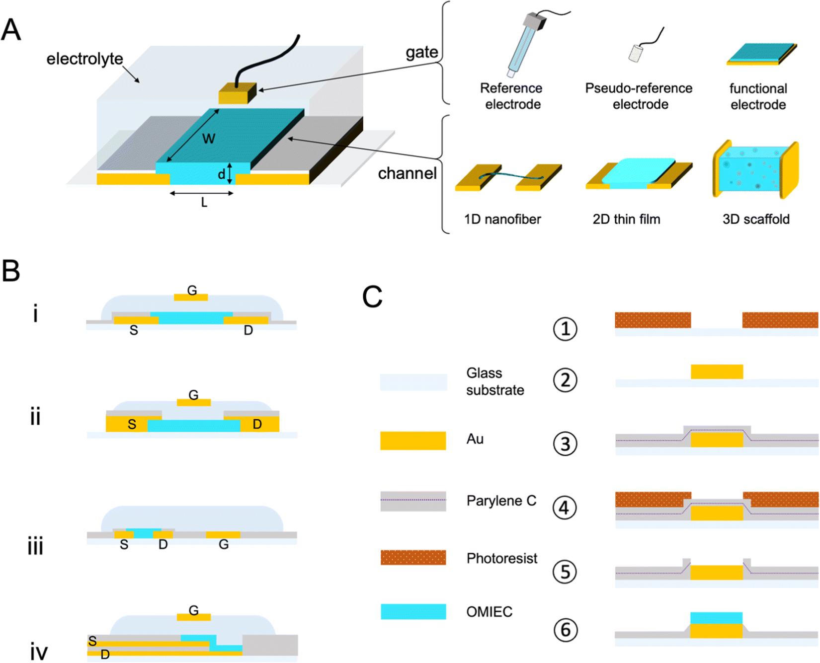 | ||
| Fig. 1 OECT architecture and fabrication. (A) The schematic represents the typical architecture of an OECT with an OMIEC film cast between the source and the drain electrodes with channel dimensions: length (L), width (W), and thickness (d). The gate electrode can be an Ag/AgCl reference electrode, a pseudo-reference electrode, or any other material, including conducting polymers, metals, or metal oxides. The OMIEC channel can be processed as a 1D fiber, a 2D-thin film, or a 3D scaffold. (B) The most common OECT architectures are bottom contact (i), top contact (ii), coplanar (iii), and vertical (iv). (C) Basic steps involved in photolithography for the microfabrication of OECT: photoresist patterning (1), Au deposition and photoresist removal (2), two layers of PaC vaporization separated by an anti-adhesive layer (3), second photoresist patterning (4), dry etching and photoresist removal (5), OMIEC coating and PaC peel-off (6). | ||
Micron-scale OECT channels are commonly fabricated using photolithography which involves multiple steps in a cleanroom facility. Such dimensions are necessary for applications where the area that the array interfaces have to be minimized, and when high spatial resolution is required. Single-cell recordings, for instance, would be possible if the size of the device matches that of the cell. Fig. 1C summarizes the key steps used in this photolithographic fabrication of OECTs. First, the metal contacts (source, drain, and gate often made of chromium/gold) are deposited on the substrate through photoresist-assisted patterning. An insulating layer, often parylene C (PaC), is vaporized over the wafer, followed by a dry etching procedure to open the channels (and the gate contacts). A second thicker layer of the insulator is then coated, including an anti-adhesive layer underneath; it is etched and peeled off after coating the OMIEC material. Except when using top contact configuration, the OECT (micro)fabrication precedes the coating of the active organic material onto the channel (and sometimes the gate too). The type of coating procedure can take many forms thanks to the versatile processability of the OMIEC. This procedure can supply high-performing devices with a critical dimension (the channel length) of only a few micrometers. While silicon wafers have been the standardized substrate, the same fabrication can be conducted on PaC-coated substrates. Such ultrathin flexible devices made possible the post-fabrication transfer of the OECT onto soft biological surfaces granting to record electrophysiological signals.57,58
Like metals, metal nanoparticles, and dielectric materials, OMIECs can be processed using mass production-oriented techniques such as inkjet printing,59,60 spray printing, or roll-to-roll fabrication.61 Although the resolution enabled by printing techniques cannot be sub micrometers; they present an appealing alternative to the time- and cost-demanding cleanroom fabrication for applications that do not require high speeds and where cost-effectiveness is more important than performance. All OMIEC-based devices (active area and contacts) can be inkjet printed in a single step on substrates incompatible with photolithography, such as paper or thermoplastics.62,63 Screen-printing technology is particularly suitable for large-scale production of OECT arrays, enabling, for example, the fabrication of 760 OECTs on one A4-sized sheet of polyethylene terephthalate (PET) with a yield of 99.7%.64 Spray-deposition of OECTs offers excellent control of the OMIEC thickness through the compressed air pressure and the number of coating cycles.65 Moreover, this technique is hardly limited by the desired type of substrate; examples include ethyl-cellulose, natural leaf, adhesive bandage, and an elastomer.66 The rheology of inks can be leveraged for volumetric printing where every component (conductor, semiconductor, insulator, and electrolyte) can be developed as a viscous ink to realize a fully 3D printed OECT. Stereolithography has appeared recently as a technique to fabricate 3D-OECT; after optimizing a mixture of OMIEC and photocurable resin, a laser head locally exposes and crosslinks the desired volumetric design.67 3D printing and stereolithography are mask-free techniques suitable for rapid prototyping as only 3D models are required. Although the resolution of both methods remained above 100 μm, about 2 orders of magnitude above the standard photolithography, fabricating out-of-plane OECTs paves the way for more complex and richer architectures.
Besides printing, the polymer films can be processed at room temperature in ambient conditions using solution-based methods ranging from spin-cast, drop-cast, and doctor blade to electrodeposition,68 electrospinning,69,70 and freeze-drying.71 The compatibility with a wide range of processing means enables the generation of films with various form factors such as scaffolds71,72 or fibers69 that can be integrated into an OECT architecture, realizing 3D or 1D channel, respectively (Fig. 1A). OMIEC fiber-based OECTs can be obtained by coating commercial fibers (often cotton or Nylon) with an OMIEC solution73 or via electrospinning of the semiconducting fiber directly.74 Fibers can be brought together, i.e., woven, to form a flexible fabric OECT inside a diaper, which can be further bio-functionalized to detect glucose levels in the sweat.75 3D channels can be generated using freeze drying, during which the solvent of the OMIEC formulation is sublimated (solid-to-gas transition), and the pores left by the sublimed solvent generate a 3D structure. Only a few solvent types can undergo sublimation (thermodynamical triple point required); therefore, the technique has been limited so far to water-based formulations. When such a polymer-based scaffold is fabricated inside a fluidic tube, and electrically connected to source–drain and gate contacts, it is possible to generate a 3D OECT. Fluidic integration supports a 3D cell culture growing inside the scaffold under constant fluid flow, while the channel current becomes a measure of cell adhesion and growth.71
2.2. Operation
The OECT operation starts with applying a voltage at the gate electrode (VG), which causes a movement of ions in the electrolyte as well as in the channel (Fig. 2A). The channel current (ID) is monitored by applying a source–drain voltage (VD). ID is proportional to the number of mobile charge carriers (holes or electrons for a p-type or n-type semiconductor, respectively) and their speed. In standard operation, the gate and drain voltages are applied with respect to the source electrode, which is grounded. The VG triggers ion injection into the channel and can as well cause the ejection of counterions from the channel if they are mobile enough, which might enhance electrochemical doping.76 Some conjugated polymers, known as polyelectrolytes, contain mobile charges that may be ejected toward the gate electrode as the bias is applied for the first time.77 In other cases, the film may contain ions that have diffused from the electrolyte. The electrolyte gating in OECTs allows for low-bias operation, typically below 1 V.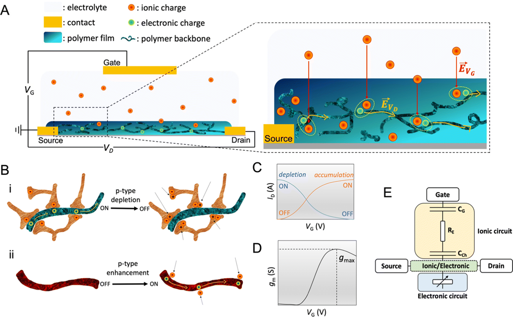 | ||
Fig. 2 OECT operation (A) schematic representation of an OECT during operation. The electric field arising from the gate electrode (![[E with combining right harpoon above (vector)]](https://www.rsc.org/images/entities/i_char_0045_20d1.gif) VG) pushes ionic charges inside the OMIEC channel. These ionic charges stabilize electronic carriers in the channel. Electronic charges can move across the channel due to voltage applied at the drain (VD), generating a source–drain current. (B) Schematic displaying two p-type OECT modes of operation (i) depletion mode device where cations penetrating the channel deplete the holes by compensating with anionic species. (ii) Enhancement mode device where penetrating anions stabilize holes. (C) Transfer curve of an OECT working in depletion mode (blue, ON to OFF) or enhancement mode (orange, OFF to ON). Adapted with permission from ref. 41. Copyright 2021, American Chemical Society; (D) transconductance vs. VG plot, i.e., the first derivative of the transfer curve. The transconductance of OECT typically denotes a maximum, gmax, reported as one of the steady-state figures of merit of OECT; (E) electronic circuit used to model OECT behavior.88 The resistor is the electrolyte resistance (RE), while the capacitors represent the capacitance of the gate electrode (CG) and the capacitance of the channel (CCh). Adapted with permission from ref. 41. Copyright 2021, American Chemical Society. VG) pushes ionic charges inside the OMIEC channel. These ionic charges stabilize electronic carriers in the channel. Electronic charges can move across the channel due to voltage applied at the drain (VD), generating a source–drain current. (B) Schematic displaying two p-type OECT modes of operation (i) depletion mode device where cations penetrating the channel deplete the holes by compensating with anionic species. (ii) Enhancement mode device where penetrating anions stabilize holes. (C) Transfer curve of an OECT working in depletion mode (blue, ON to OFF) or enhancement mode (orange, OFF to ON). Adapted with permission from ref. 41. Copyright 2021, American Chemical Society; (D) transconductance vs. VG plot, i.e., the first derivative of the transfer curve. The transconductance of OECT typically denotes a maximum, gmax, reported as one of the steady-state figures of merit of OECT; (E) electronic circuit used to model OECT behavior.88 The resistor is the electrolyte resistance (RE), while the capacitors represent the capacitance of the gate electrode (CG) and the capacitance of the channel (CCh). Adapted with permission from ref. 41. Copyright 2021, American Chemical Society. | ||
OECTs display two operation modes: depletion and accumulation (enhancement). The distinction between these two modes lies in the intrinsic doping state of the channel material. If the channel is made of a conducting (doped) polymer, the device operates in depletion mode (ON to OFF). In contrast, an undoped polymer with negligible electronic conductivity will work in enhancement mode (OFF to ON). An example of a depletion mode OECT comprises a poly(3,4-ethylenedioxythiophene):poly(styrene sulfonate) (PEDOT:PSS) channel (Fig. 2B-i). The net negative charges of the PSS compensate for the positive charge carriers (holes) of PEDOT, rendering the film conducting in its neutral state, with reported electrical conductivities as high as 4000 S cm−1 (with sulfuric acid post-treatment).31 A positive voltage at the gate with respect to the source electrode injects electrolyte cations that pair with the PSS anions while holes are extracted at the drain electrode. The “dedoping” of the PEDOT:PSS film during the OECT operation (VG magnitude increasing to a more positive value) causes the ID to decrease (Fig. 2C). This process is reversible: when VG is reversed (or stopped), cations leave the channel, and PSS once more forms ionic bonds with PEDOT, oxidizing it back to its conducting state.
It is also possible to operate PEDOT:PSS in enhancement mode OECT if the film contains aliphatic amines as de-dopants, for instance, polyethyleneimine (PEI),78 diethylenetriamine (DETA),79 and 1,8-diazabicyclo[5.4.0]undec-7-ene (DBU).80 In this case, the material's conductivity is low, but there are still states that can be filled with electrochemically injected charges. In a p-type enhancement mode OECT, a negative VG pushes anions inside the film, stabilizing holes injected along the backbone (Fig. 2B-ii). The electrostatic coupling between electronic and ionic charges increases the conductivity of the channel, switching the device from an OFF to an ON state (Fig. 2C). Other enhancement mode OECTs use conjugated polymers that contain polar, hydrophilic units, such as conjugated polyelectrolytes with charged units on side chains or polymers with ethylene glycol (EG) side chains. These polymers can be hole (p-type) or electron (n-type) transporters. One example of n-type OECT channel material is poly(benzimidazobenzophenanthroline) (BBL). The planarity and rigidity of the BBL backbone promote electron delocalization and facilitate intramolecular charge transfer. The high performance of enhancement mode BBL OECTs have been leveraged to build complementary circuits81–83 and an ion sensor,84 as well as neuromorphic devices.85 Furthermore, BBL represents the first demonstration of an n-type depletion mode OECT, where BBL was chemically reduced with PEI in printable ethanol-based ink.82 After thermal activation under an inert atmosphere, BBL:PEI films displayed an electrical conductivity as high as 8 S cm−1 and excellent thermal, ambient, and solvent stability. Recent work also showed the combination of p and n-type polymers in the form of a bulk heterojunction, where a p-type 6H-pyrrolo[3,2-b:4,5-b′]bis[1,4]benzothiazine ladder (PBBTL) polymer was blended with BLL, producing an ambipolar OECT.86 By optimizing the mass ratios of the individual polymers, the authors tuned the transport properties of each component of the bulk heterojunction, achieving a bi-continuous network of homogeneously distributed junctions between the PBBTL and BBL interfaces. Such combinations allow for extending the operation regime of OECTs. Furthermore, polymers displaying different redox states over a wide electrochemical window, such as polyaniline, can be leveraged to build single-component complementary circuits.87
The transconductance  is usually considered the most important figure of merit of OECTs as it quantifies the amplification factor. It is often reported as the maximum transconductance (gmax) when comparing the performance of different OECTs of the same geometry (Fig. 2D). Bernards and Malliaras were the first to develop a mathematical prediction of OECT gm by considering the conjugated polymer channel as the conjunction of an electronic circuit and an ionic one (Fig. 2E).88 The electronic circuit is represented by a variable resistor corresponding to the conductivity of the channel that varies in function of the gating. It involves the electronic charges in the channel that drift under the application of a source–drain voltage (VD in Fig. 2A). The ionic circuit is composed of capacitors in series with a resistor. The ionic circuit describes the flow of ions toward the semiconductor bulk and is represented by a resistor (flow of ions) in parallel with a capacitor (storage of ions). The ions drift under the application of VG (VG in Fig. 2A). Bernard's model considers a purely capacitive process for the film and assumes a voltage-independent electronic mobility.89,90 The model provides a good approximation of the steady-state performance of OECTs at saturation conditions and allows for the prediction of the gm as expressed in eqn (1):91
 | (1) |
 channel dimensional ratios before saturating for high ratios. They showed that the VG corresponding to gm,max depended on VD and the channel thickness and length. Moreover, the authors adjusted their model to include the influence of contact resistance, which was shown to be the origin of the gm,max saturation at high channel ratios, and more pronounced at low VD. Overall, this model allows to optimize the gm by adjusting the channel ratio and biasing conditions to operate the OECT at voltages that lead to highest gm.
Another metric in the equation above is the product of μC*, which is commonly used to benchmark materials' mixed conduction performance. Here, C* reflects the extent of ion penetration, transport, and storage ability of the OMIEC film. The ion uptake in the bulk of the channel yields high capacitance, hence, excellent signal amplification. The μ accounts for the transport of the electronic charges across the channel. Both of these parameters are typically VG-dependent. Furthermore, the size, charge, and polarity of ions are parameters that influence their penetration and mobility inside the polymer film, thus influencing the μC*.93–95 Cendra et al. studied the effect of various compensating anions on the performance of a p-type enhancement mode OECT.94 They found that larger and less hydrated anions lead to OECTs with higher gm. Flagg et al. demonstrated anion-dependent doping and charge transport of p-type enhancement mode OECTs, where higher drain currents and lower threshold voltage were observed with a molecular anion (PF6−) rather than a smaller atomic anion (Cl−).30,93 Finally, OECT performance is affected by the nature and the geometry of the gate electrode as it dictates the amplitude of the gate voltage drop across the channel.96,97 In the case of a non-polarizable gate electrode such as Ag/AgCl, most of the applied gate voltage drops at the channel/electrolyte interface. For polarizable gates, an electrochemical double-layer capacitance forms at the electrolyte interface, which, for maximum channel current modulation, should be much higher than the capacitance of the channel. It is thus required to have a large area gate when using polarizable gate electrode materials to operate the device efficiently.
Although the interactions of ionic and electronic charges in the bulk of the channel endows OECTs with high gm, volumetric charging leads to a slow operation.1 The response time of the OECT, i.e., the switching speed, is governed by how fast each type of charge travels inside the channel. For PEDOT:PSS, it is often the ionic charge transport that is identified as the speed-limiting process, as hole transport is relatively faster, and the response time can then be estimated from the RC time constant of the ionic circuit.88 The response time of the OECT thus depends on the capacitance of the material, which increases with film thickness.91 The film's thickness can thus be optimized to better match the requirements of the end application with a trade-off between the gain and the bandwidth. The following sections will detail these performance metrics.
2.3. Characterization of an OECT
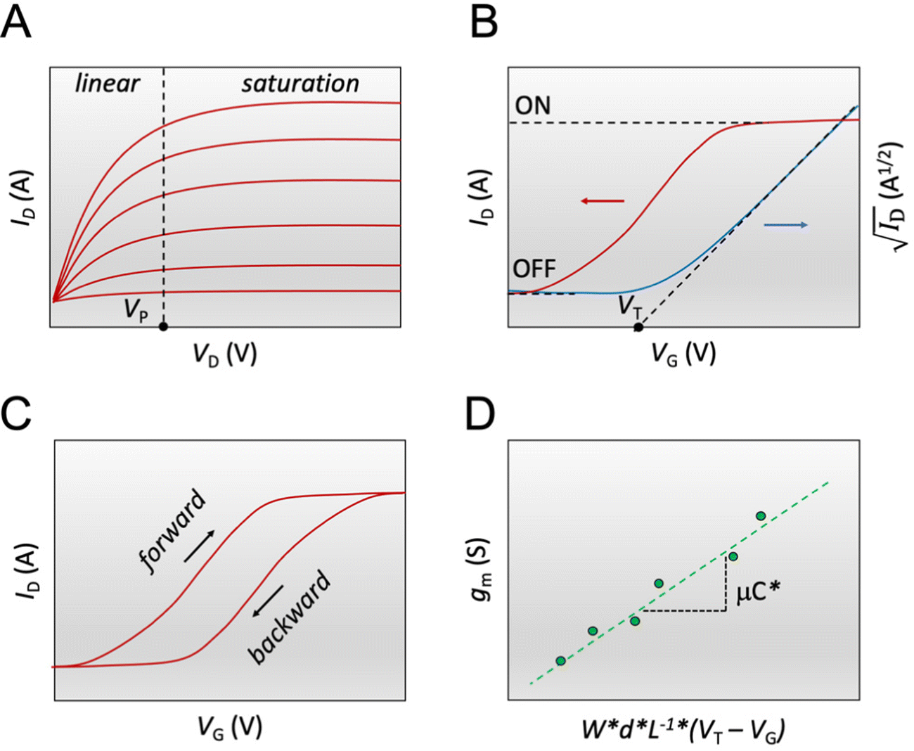 | ||
Fig. 3 The steady-state figures of merit of an OECT. (A) Output characteristics show the ID evolution as a function of VD. Each line represents the device current at a constant VG. The pinch-off voltage VP is marked. (B) The transfer curve (red) shows the evolution of ID as a function of VG. The ON/OFF ratio is calculated from the ratio of the maximum ID at saturation (ON) and the current at saturation in the OFF state (OFF).  as a function of VG (blue) with VT obtained from the x-axis intercept; (C) transfer curve hysteresis; (D) the μC* product as an OECT figure of merit. The gm of each OECT measured at the saturation regime is plotted as a function of its channel geometry and biasing conditions. Each point corresponds to one OECT measurement, and all the measurements give a linear relationship according to eqn (2), where the slope is the μC* product. as a function of VG (blue) with VT obtained from the x-axis intercept; (C) transfer curve hysteresis; (D) the μC* product as an OECT figure of merit. The gm of each OECT measured at the saturation regime is plotted as a function of its channel geometry and biasing conditions. Each point corresponds to one OECT measurement, and all the measurements give a linear relationship according to eqn (2), where the slope is the μC* product. | ||
The transfer curve is obtained by recording the channel current as the VG is swept and the drain electrode is polarized at a constant potential with respect to the source (Fig. 3B). The VD is typically chosen to be in the saturation regime. We obtain key parameters from transfer curves such as the VT, ON/OFF ratio, and gm. The VT can be determined by plotting the square root of the ID as a function of VG (Fig. 3B). The linear portion of the slope with the maximum magnitude is extrapolated, and the intersection with the x-axis gives the VT.100 The accuracy of this method is, however, questionable given the voltage dependence of μ,101 the presence of parasitic resistance, and the limited speed of charges at low ionic dopant concentrations.30
V T is generally regarded as the voltage that fills trap states in the semiconductor for the conduction to occur in field effect devices.102,103 In OECTs, it is mainly governed by the energetics of the channel material (ionization potential or electron affinity) and the film's readiness for ion penetration. VT is often correlated with the electrochemical potential that corresponds to the UV-VIS polaron absorption onset. It also often matches the electrochemical onset potential (reduction or oxidation onset) identified in cyclic voltammetry curves.94 Controlling VT has been of particular interest for OECT-based sensors104 and logic circuits as it dictates the noise margin and the circuit power consumption.105VT has been shown to vary by the gate electrode type and electrochemical potential,37,105,106 the side-chains of the polymer which affect ion penetration,107 the type and concentration of ions in the electrolyte,93,94,104 and device architecture such as dual-liquid gate,108,109 microfluidic channels13 or channel aspect ratio.110
The ON/OFF ratio is defined as the ratio of the maximum channel current when the OECT is turned on (for an enhancement-mode transistor) and the current at OFF state (at VG = 0 V if the material is undoped at this voltage) (Fig. 3B). Transistors with large and stable ON/OFF ratios are preferred for logic circuits and neuromorphic applications since high and static ON currents allow for effective signal output. Low OFF currents consume less power and cause less background noise for sensors.64 High ON/OFF ratios are essential for biosensors' response as it improves the signal-to-noise (SNR) ratio of the device. Thus lower limits of detection can be achieved.13,111 To this end, enhancement mode devices are preferred as they generally present higher ON/OFF ratios than depletion mode transistors (due to incomplete dedoping of the channel), and thus offer a more extensive range of current modulation.
The first derivative of the transfer characteristics corresponds to the VG-dependent gm at a chosen VD in the saturation regime (Fig. 2D). Eqn (1) showed that gm in the saturation region depends on the channel dimensions, the channel material properties (μOECT and C*), VT, and VG (Fig. 3D). For the same material and device geometry, any condition that impacts VT will naturally change the gm. The reported gm values are typically normalized by the width of the channel transistor, film thickness, or sometimes the VD, indicating the lack of a standard.2,77,112 As gm is one of the main performance metrics, it is crucial to have a standardized way of reporting it for a fair comparison between different devices. The following equation normalizes the gm with the device geometry:
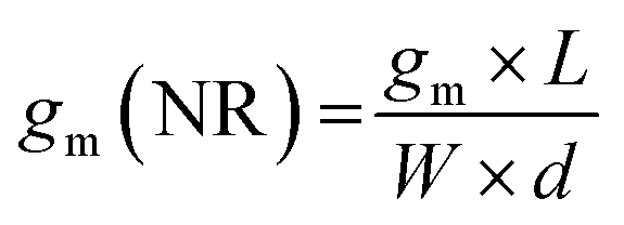 | (2) |
When determining gm(NR), we stress the importance of accurate thickness measurements. While it is common to normalize the gm by the thickness measured from a film cast using the same conditions but on a usually much bigger electrode (typically made of gold), these values do not necessarily correspond to the film thickness in the microscale channel, especially when it is fabricated using the photolithographic process described above. The thickness mismatch is severe where the channel opening leads to a significant difference in the polymer's wetting, and thus coating, compared to a large electrode surface. Even the thickness of the film cast on a metal electrode microfabricated on the same substrate and located in the vicinity of the channel may differ from that in the channel. For accurate channel thickness measurements, atomic force microscopy measurements are recommended, where the film is scratched down to the substrate, typically using a hard tip in contact mode. This method is, however, time-consuming and destructive to the channel. An alternative is fabricating a separate device without the metal contacts through the same protocol used for patterning and measuring the film thickness with a profilometer. This way, the channel wetting, and coating properties can be routinely replicated on a separate substrate and used only for film thickness estimations. As for the length and width, they should be measured each time after fabrication to eliminate batch-to-batch differences. We define the length of the channel as the distance between the source and drain electrodes, and thus do not consider the overlap between the channel and the contact electrodes.
 | (3) |
 .113 The relaxation of the ID over time is fitted with a mono-decay exponential function, where the characteristic time corresponds to the time response of the OECT (τOn).
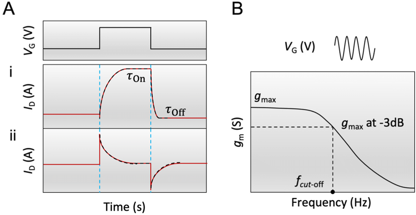 | ||
| Fig. 4 The transient characteristics of an OECT (A) ID in response to a square VG pulse is measured while VD is maintained constant. Two main types of behaviors are observed: a monotonic relaxation of ID towards the steady-state value (i) or a “spike and recovery” behavior (ii). The fit is an exponential decay function (black dotted lines), from which the characteristic time is extracted; (B) gm is measured in response to a sinusoidal VG pulse while VD is maintained constant. The frequency corresponding to the value of gmax at −3 dB (around 0.707gmax) represents the cut-off frequency of the device that can be used to estimate τOn. | ||
According to eqn (3), when the electronic transport is faster than the ionic charging, ID relaxes monotonically to its steady-state value (Fig. 4A-i). When the electronic transport is instead the limiting factor, ID displays a spike beyond the final steady-state current before relaxing exponentially towards the final current, demonstrating a “spike and recovery” behavior (Fig. 4A-ii). The monotonous relaxation and “spike-and-recovery” behavior of channel current have been observed for various OECTs.91,98,114–116 The OECT transient characteristic is thus generally measured from the ID response to a VG pulse, under a constant VD (chosen in the saturation regime). The VG pulse amplitude and period are adjusted depending on the material and channel geometry. For example, a large channel geometry typically leads to slower devices. Hence the pulse length should be correspondingly extended. Using a long gate pulse would be appropriate to obtain a current response with high resolution for a good quality fit.
Another method to estimate τOn is through the impedance matching method, detailed below for the determination of μOECT. Here, τOn can be calculated from τOn = RS·CCh after modeling the impedance spectra with an equivalent circuit model or through the cutoff frequency (fc), which describes the frequency upper boundary that OECTs can achieve for signal acquisition and amplification (Fig. 4B), based on eqn (4):117
 | (4) |
Some strategies have been implemented to shorten the OECT response time to meet the needs of the end application. In the first method, the film is made thinner, or the dimensions shrink (mostly by reducing W) as  .90 Given the relationship between channel geometry and gm (eqn (1)), L should be as small as possible to maximize gm, while W and d should be chosen considering the application. For instance, when using OECTs to measure slow signals of low amplitude, W and d should be increased, while a thinner and narrower channel will be more beneficial for fast signals. A second method is to optimize the biasing conditions. Friedlein et al. demonstrated that by operating OECTs at VD = VSTEP, OECTs could respond more than 30 times faster than the speed of their ionic charging circuit, where:98
 | (5) |
While Bernard's model marks the first attempt to predict OECTs’ transient response, the simplifications introduced in the model limit its accuracy, which was addressed in more recent models. For example, Friedlein et al. considered an exponential distribution of the density of states. They accounted for the influence of the charge carrier density on μOECT to address the constant charge carrier mobility assumed in Bernard's model.124 The authors proposed that their non-uniform mobility model will be helpful in better understanding the transient behavior of OECTs. Other models have improved Bernard's model and given a physical interpretation to the factor f (see eqn (3)). Gentile et al. proposed a hybrid model combining Bernard's and the equivalent circuit models, associating f with the penetration depth of ions in the film bulk, where the output characteristics of the device depend explicitly on the size and charge of the ions species.125 Fitting the model to channel current response to triangular gate voltage pulses could describe the transient response of OECTs and be used to calculate ion diffusion coefficients in solution, where the lag between the doping and dedoping peak current at different frequencies was characteristic of a specific system diffusivity. They used this method to discriminate electrolyte characteristics such as the cation and anion type and their concentration. Based on equivalent circuits, Faria et al. introduced a model that could accurately predict OECT transient behavior and provide an experimental method to determine the factor f.116 By fitting the gate and channel current response to a VG pulse, the model yields impedance circuit values such as the impedance (capacitance and resistance) of the polymer in the channel, the electrolyte resistance, and, ultimately, the factor f. IG that flows into the channel is split between the source and drain electrodes. The authors interpreted factor f as the fraction of this current measured at the drain electrode and demonstrated that it was gate and drain voltage-dependent. They further speculated that f also depends on the channel geometry and gate-channel distance. Faria model was extended to describe the behavior of cell membrane integrated OECTs and to effectively extract the corresponding membrane impedance characteristics, parameters that define their health status. For an in-depth analysis of the current OECT models and their limitations, along with the physical phenomena considered, we would like to refer the reader to recent literature reviews and ref. 22, 90, 103, 126 and 127.
3. Characterization of mixed transport properties of OECT channel
3.1. Volumetric capacitance (C*)
The capacitance of a material is often determined from the electrochemical impedance spectrum (see Fig. 5A for an exemplary spectrum) recorded using electrochemical impedance spectroscopy (EIS). The EIS setup involves a three-electrode system with the OMIEC film addressed as a working electrode (WE), a reference electrode (RE), and a counter electrode (CE), all immersed in the electrolyte. The CE should have a much larger C than the WE to ensure that the kinetics of the reactions occurring at the counter do not inhibit those occurring at the WE.128 The spectrum is acquired by applying a small AC modulation (typically 10–50 mV) with varying frequencies (typically 106–10−1 Hz) on a DC offset. The voltages are applied to the WE with respect to the RE. The spectrum will naturally change as a function of the offset voltage and for undoped films, the spectrum should be acquired at a potential that maximizes the C of the OMIEC film. For intrinsically doped polymers such as PEDOT:PSS, the voltage is set at the open circuit potential. Once the data are acquired, the C can be extracted in two ways. The first approach relies on eqn (6):129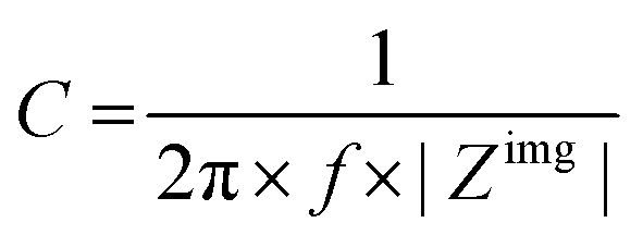 | (6) |
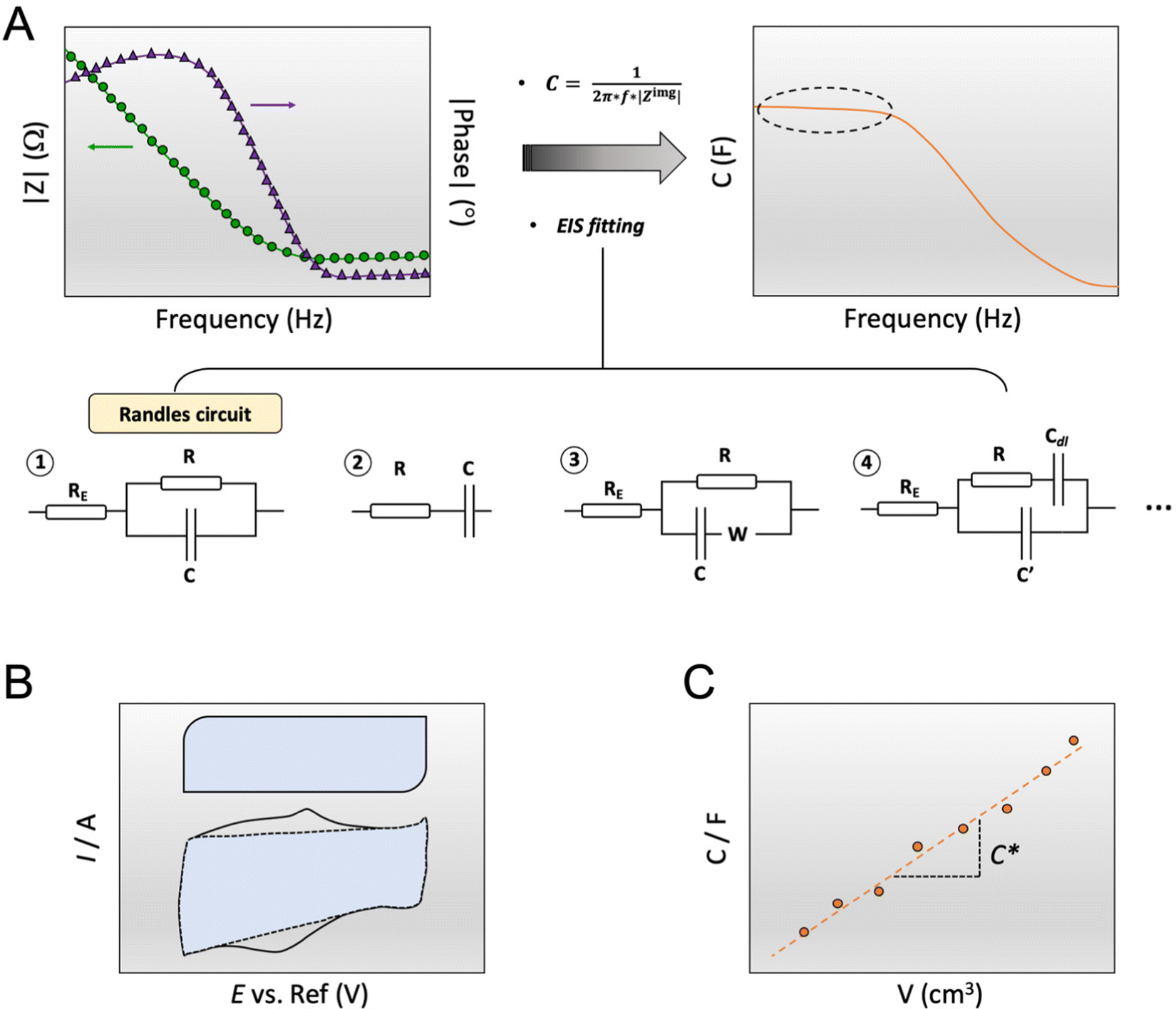 | ||
| Fig. 5 Determination of C*. (A) C extraction from EIS data (left plot: dots and triangle represent the impedance modulus |Z| and the impedance phase, respectively) either by applying eqn (6) (right plot, the marked area shows the plateau at low-frequency region) or by fitting the data with an equivalent circuit modeling. The most common equivalent circuit models are shown at the bottom; (B) C extraction from the integration of a cyclic voltammogram curve, represented by the blue area, according to eqn (8). The top box-like curve represents an ideal capacitive material, while the bottom curve corresponds to an OMIEC that presents redox reactions; (C) C vs. volume curve. The slope yields C*. | ||
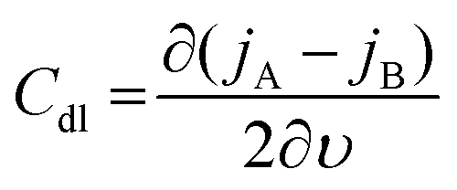
The C extracted this way includes all the possible capacitive contributions of the system. In the case where a material deviates from an ideal capacitor behavior, evidenced by an impedance phase angle much lower than 90° at low frequencies, the contribution of a double layer capacitance, Cdl, becomes significant. Such materials are those with low ionic mobility or high ion injection barrier, thus the impedance phase spectrum is an important aspect to analyze to determine whether a material would work in an OECT device. Cdl can be calculated as the slope of the difference in anodic (jA) and cathodic (jC) current density (A/unit area), measured in the non-faradaic region (at a potential that does not involve any electron exchange reactions) of the cyclic voltammogram as a function of the scan rate υ:130
 | (7) |
Besides EIS, cyclic voltammetry also allows the C to be estimated (Fig. 5B). In the absence of faradaic reactions, the cyclic voltammogram can be integrated to provide C*, according to eqn (8):89
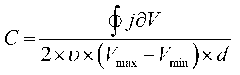 | (8) |
Lastly, to extract the C*, one should divide the obtained C value by the corresponding film volume (Fig. 5C). For accurate estimation of C*, the C of films with varying geometries should be measured. The extracted capacitance should scale linearly with the film geometry with the slope of the curve, yielding C*.2,91 The offset of the linear fit can indicate the presence of an ion injection barrier or ion accumulation at the polymer film/electrolyte interface.91 A saturation at high film volumes may be due to an incorrect speed used to evaluate the charging currents.
3.2. Electronic charge carrier mobility (μOECT)
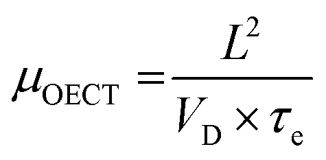
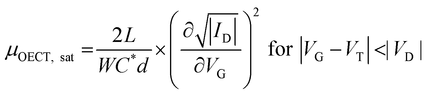
While methods for extracting electronic mobility in (O)FET devices and their limitations are well established and documented in the literature,139,140 the co-presence of ionic and electronic charges in the OECT channel prevents the direct translation of these techniques to extract OECT electronic charge carrier mobility in OECTs (μOECT). The determination of μOECT is based on measuring the electronic charge carrier transit time (recall, τe) from a time or frequency domain IG analysis. The first approach applies an IG pulse while the channel current is monitored at a constant VD (Fig. 6A-i).88 The slopes of IDvs. time curves as a response to IG pulses with various magnitudes is plotted as a function of IG. The τe is then extracted using eqn (9):88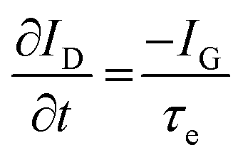 | (9) |
| ΔIG = 2π × f × τe × ΔID | (10) |
 | (11) |
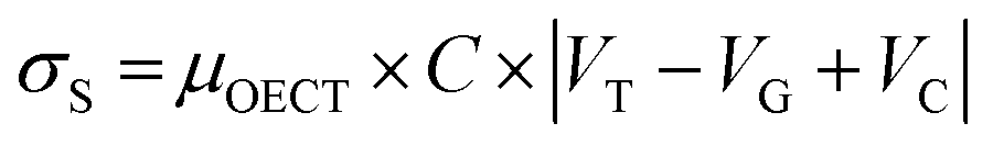
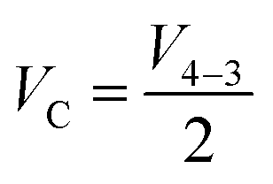
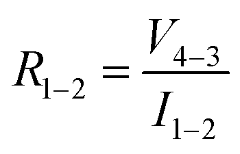
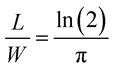 in accordance with square van der Pauw structures.142 The current injected between contacts 1 and 2, I1–2 can then be expressed in terms of the sheet resistance σS:
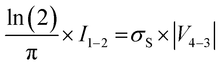 | (12) |
 | (13) |
 | (14) |
 | (15) |
 | (16) |
 | (17) |
 | ||
Fig. 6 Determination of μOECT. (A) The μOECT is calculated from the electronic charge carrier transit time τe using eqn (9). The τe can be determined by gate current analysis at time (i) or frequency (ii) domain. Adapted with permission from ref. 118. Copyrights 2015, AIP Publishing LLC; (B) schematic of the electrochemical van der Pauw measurement setup (left) and time response of microscopic four-contact structures during electrolyte gated van der Pauw measurements. The voltage drop on the sample between the sensing contacts 4 and 3 is measured in time while varying the applied gate voltage VG. Adapted with permission from ref. 141. Copyright 2021 Wiley-VCH; (C) the [μC*] product extracted from the slope of Fig. 3C is plotted as a function of the product of [μOECT] and [C*] determined independently for various OMIECs, where the dashed line corresponds to a 1![[thin space (1/6-em)]](https://www.rsc.org/images/entities/char_2009.gif) :1 agreement. In particular, p(g2T-T), p(g2T-TT), and p(gBDT-g2T) are p-type enhancement mode OECT materials based on glycolated thiophene, thiophene–thienothiophene, and benzo[1,2-b:4,5-b′]dithiophene (BDT)-thiophene-based backbones, respectively. TOS, PSS, PSTFSI and PMATFSI, and DS, are molecular, polymeric, and biological anionic dopants complexed with PEDOT, namely tosylate, poly(styrene sulfonate), (trifluoromethylsulfonyl)sulfonylimide (styrene or methacrylate backbone and Li+ as the counter ion), and dextran sulfate, respectively. These materials are suitable for p-type depletion mode operation. p(gNDI-g2T) is a glycolated naphthalene diimide-based n-type material. PTHS is a thiophene-based, undoped conjugated polyelectrolyte with sulfonate-terminated alkyl chains. Adapted from ref. 2 under the terms of the Creative Commons Attribution 4.0 International License. Copyright 2017, Nature Publishing Group. :1 agreement. In particular, p(g2T-T), p(g2T-TT), and p(gBDT-g2T) are p-type enhancement mode OECT materials based on glycolated thiophene, thiophene–thienothiophene, and benzo[1,2-b:4,5-b′]dithiophene (BDT)-thiophene-based backbones, respectively. TOS, PSS, PSTFSI and PMATFSI, and DS, are molecular, polymeric, and biological anionic dopants complexed with PEDOT, namely tosylate, poly(styrene sulfonate), (trifluoromethylsulfonyl)sulfonylimide (styrene or methacrylate backbone and Li+ as the counter ion), and dextran sulfate, respectively. These materials are suitable for p-type depletion mode operation. p(gNDI-g2T) is a glycolated naphthalene diimide-based n-type material. PTHS is a thiophene-based, undoped conjugated polyelectrolyte with sulfonate-terminated alkyl chains. Adapted from ref. 2 under the terms of the Creative Commons Attribution 4.0 International License. Copyright 2017, Nature Publishing Group. | ||
Finally, note that the electronic charge density varies across the film as it depends on the electrochemical potential (which has a changing profile from source to drain),146 resulting in non-uniform, voltage-dependent charge transport properties.124 The voltage dependence of μOECT has also been attributed to band fillings (i.e., at high doping potentials, HOMO or LUMO is filled with electronic charges, and there is a lack of empty states to allow the charge to hop onto) or contact effects. On the other hand, an ionic charge injection barrier causes the C to be voltage-dependent.2,146,147 Thus, it is essential to keep in mind that the application of eqn (1), from which we can obtain the different steady-state figures of merit of OECT, does not take into account these considerations, and therefore voltage-dependent must be taken into account when reporting/interpreting data.
3.3. Ion mobility and ion motion
Monitoring ion transport within the channel and quantifying ion mobility is critical to improving OECT performance, particularly the switching speed and capacitance. While methods have been developed to estimate the mobility of electronic charge carriers, the ion motion in the film is not trivial to monitor, and ion mobility is more challenging to calculate due to the accompanying movement of electronic charges. Ion transport in a conjugated polymer film depends on the nature of ionic species (size, water affinity, and interactions with the counter ion), the strength of the electrical field, and on the polymer film morphology and interactions with the electrolyte (swelling). For an OECT operating in aqueous electrolytes, the channel needs to interact with hydrated ions; hence integrating polar components, such as EG units or charged groups in the polymer side chains, has been a successful strategy to enhance the ion transport ability of the films.27,121 Increasing the segmental motion of the side chains by introducing alkyl spacers was suggested to improve ionic conductivity further.148 Besides the nature of chemical components that make the film, the film microstructure and morphology affect ion transport.25,149 For example, including a cross-linker such as 3-glycidoxypropyltrimethoxysilane (GOPS) in the PEDOT:PSS formulation makes the film denser (less porous), decreasing the speed of ions.134 The addition of EG in the polymer dispersion improves the electronic charge transport by rendering PEDOT and PSS phases more homogenous and increasing the PEDOT-rich content, which, in turn, reduces the ability of ions to reach these PEDOT-rich areas.25,149One method to study ion motion and extract their mobility involves a spectroelectrochemistry setup where the film's optical transmission profile or UV-VIS spectrum is monitored while it is electrochemically doped (Fig. 7A). This is possible as the electronic excitations have signatures in the optical spectrum of OMIEC films. In this experiment, the ion motion in the film is restricted to two dimensions as the film is insulated everywhere except for an opening to the electrolyte where the reference electrode is dipped.134,149,150 Application of a potential between this electrode and the other end of the film forces ions to penetrate the film and travel towards its end. As the ions move, they change the transmission profile of the film (Fig. 7A), causing a de-doping (or doping) front to move as fast as their speed. Monitoring the evolution of this “moving front” over time allows us to estimate ionic mobility.149,151 Stavrinidou et al. proposed a model based on these experiments to evaluate ion drift mobility inside conducting polymer films (e.g., PEDOT:PSS).134,151 By modeling the moving front as two resistors in series (one ionic for the dedoped part and one electronic for the doped region), the authors related the moving front length (or drift length of the injected ions), ![[small script l]](https://www.rsc.org/images/entities/i_char_e146.gif) , to the total resistance of the film according to eqn (18):
, to the total resistance of the film according to eqn (18):
 | (18) |
| 2 = 2 × μP × Vapplied × t | (19a) |
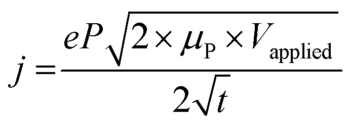 | (19b) |
 | ||
| Fig. 7 Monitoring ion transport in OMIEC films. (A) (i) Moving front measurement configurations: a spectro-temporal moving front experiment using a white light source/fiber spectrometer (left) and spatio-temporal moving front experiment using a microscope objective (right) at a specified distance X from the edge of the film–electrolyte interface to track the motion of injected ions. In all cases, the time of application of bias is t = 0 s. (ii) The absorbance spectra and the corresponding time–wavelength color plot for X ≈ 1 mm for a PEDOT:PSS film (0 vol% EG). The right panels show the absorbance spectra from t = 1 s (blue) to t = 90 s (red) using the same color scheme. (iii) The optical images of the moving front at t = 0, 10, 30, and 40 s. (iv) Normalized absorbance intensity of the film at a distance X as the de-doping front propagates, validating the agreement between the spectro-temporal (red symbols) and spatio-temporal moving front experiment (black symbols) (X values as noted). The normalized absorbance intensity profiles of the same film obtained from microscopy studies are shown as insets (blue: t = 5 s, red: t = 45 s. Adapted with permission from ref. 149. Copyright 2016, Royal Society of Chemistry; (B) instrumentation schematic of in situ electrochemical strain microscopy (ESM) using dual-amplitude resonance tracking centered around the contact resonance frequency. ESM images from P3HT thin films overlaid with AM-FM pixels corresponding to the lower 21% (i) and upper 24% (ii) of AM-FM stiffness (frequency) map data, where higher frequency means higher elastic modulus. The pixels show anti-correlation between AM-FM and ESM data, with morphology ranging from more amorphous (softer) to more crystalline (stiffer) correlated with enhanced or diminished ion uptake. Adapted with permission from ref. 40. Copyright 2017, Nature Publishing Group; (C) Comparison of topographic features of two ratios of DPP-DTT:polystyrene (PS) nanowire blends upon PF6− doping. (i) Topography (top) and 840 cm−1 PiFM pixels corresponding to PF6− signal (bottom), for a 2:8 film. Here the nanowire film was doped at approximately half of the film. The PF6− ions do not appear in the topography but are very obvious in the PiFM image, indicating that the ions have penetrated the matrix. (ii) 1:0 film topography focusing on a similar doping junction (top) and PF6− corresponding image (bottom). Here, the topography clearly shows the PF6− ions, consistent with the interpretation that the ions are not penetrating the film. The PiFM image shows the same contrast everywhere, consistent with most of the anions staying closer to the surface. Both films were doped with 100 mM KPF6 at −0.85 V. Adapted with permission from ref. 153. Copyright 2021, American Chemical Society. | ||
Besides monitoring the transmission profiles, the same technique could monitor the evolution of the UV-VIS spectrum (Fig. 7A-ii). Doing so allows us to get more information about the preferential movement of ions to different parts of the film as the optical features at different wavelengths inform about film morphology, as they may belong to differently aggregated parts of the films. As such, ion transport-morphology relationships can be investigated. Moving front measurements, and the above analytical model, are currently the only method that allows estimating ion mobilities in OMIEC films. However, the above model has not yet been applied to intrinsically un-doped polymers, possibly due to experimental difficulties arising from ion/charge injection barriers at large geometries. This highlights the need for new techniques and models. Furthermore, while the Cottrell equation has often been (mis)used to extract ion diffusivity from chronoamperometric measurements,36,38 we would like to emphasize that the Cottrell equation does not account for the significant effect of RC charging in OMIEC films, thus leading to inaccurate ion mobility values. Moreover, the Cottrell equation assumes a surface-related redox reaction event, as opposed to the volumetric and often electrostatics-driven charge compensation in OMIECs.
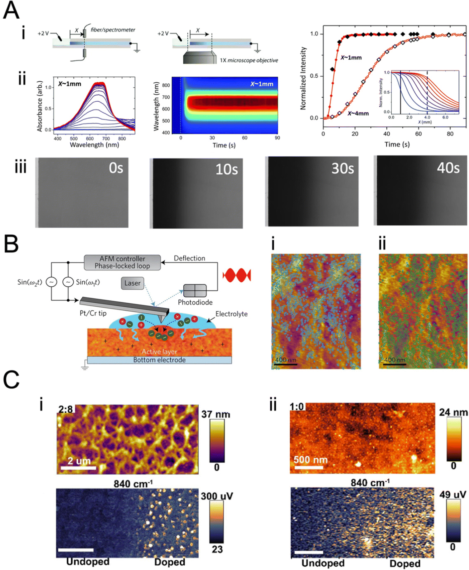
Electrochemical strain microscopy (ESM)40 and infrared photo-induced force microscopy (PiFM)152 are two other methods that can be used to monitor ion motion in films. In ESM, an AC bias is applied to the AFM cantilever in contact with the polymer film immersed in an electrolyte, inducing local oxidation/reduction upon simultaneous ion injection/expulsion from the film (Fig. 7B). The local swelling/de-swelling is monitored as a function of the ESM amplitude.93,153 Giridharagopal et al. first demonstrated this technique using poly(3-hexylthiophene-2,5-diyl) (P3HT) films.40 The ESM images overlaid with stiffness pixels of P3HT revealed heterogeneous local swelling of the film under electrochemical doping, where morphology ranging from more amorphous (softer, Fig. 7C-i) to more crystalline (stiffer, Fig. 7C-ii) correlated with enhanced or diminished ion uptake, respectively. This work represents the first direct visualization of ion uptake-induced morphological changes. The ESM technique was later successfully applied by the same team to poly[2,5-(2-octyldodecyl)-3,6-diketopyrrolopyrrole-alt-5,5-(2,5-di(thien-2-yl)thieno[3,2-b]thiophene), DPP-DTT nanowires, showing volumetric electrochemical operation.153 Overall, ESM represents a powerful technique to correlate nanoscale variations in ion uptake with morphological changes therein and polymer packing. However, this method is still vastly underused, possibly due to operational challenges.
PiFM allows monitoring of the IR signature of the ions injected into the films by measuring the IR-induced dipole–dipole interactions between the AFM probe tip and substrate (Fig. 7C). This technique was successfully applied to monitor the uptake of PF6− anion (by following the anion characteristic IR P–F stretch absorption peak) while mapping the film morphology of different dry polymers such as (poly[2,5-bis(thiophenyl)-1,4-bis(2-(2-(2-methoxyethoxy)ethoxy)ethoxy)benzene-PB2T-TEG, poly(3-((2-(2-methoxyethoxy)ethoxy)methyl)thiophene-2,5-diyl)-P3MEEMT, and DPP-DTT) and film architectures (thin films and nanowires).30,152,153 When the nanowire film was electrochemically doped up to its half section, the PF6− ions did not show up in the topography but were very obvious in the PiFM image, indicating that the ions penetrated the matrix (Fig. 7C-i). Conversely, when the PF6− ions could not penetrate the bulk of the film, the ions were visible on the surface morphology, and the PF6− signal was observed uniformly on the surface (Fig. 7C-ii). PiFM can thus give valuable information on the spatial distribution of dopants (ions), allowing to map ion uptake distribution in crystalline and amorphous parts of the film.30 However, PiFM requires vacuum conditions and, thus, does not reflect real-time ion injection into the film. Furthermore, its use for conjugated polymers has been restricted to p-type polymers, as there is yet to find a cation with a characteristic IR signature like PF6− for n-type materials ion uptake imaging.
Glow Discharge Optical Emission Spectroscopy (GDOES) is an analytical technique that provides quantitative measurements of the elemental depth profile of a substrate. GDOES was useful in investigating ionic charge depth distribution profiles within conjugated polymer films. Flagg et al. demonstrated through GDOES measurements that both ions from KPF6 could diffuse within the P3MEEMT polymer film before electrochemical doping as opposed to TBAPF6.76 Conversely, none of the ions from the Cl− based electrolytes could enter the film. Before electrochemical doping, the passive diffusion of the non-compensating ion within the film was considered responsible for the earlier oxidation onset. The oxidation of the films was hypothesized to occur first through cation expulsion, followed by the injection of the compensating anion from the electrolyte. Another technique that can be used to track ion distribution inside the film is Secondary Ion Mass Spectrometry (SIMS).36 Despite its higher resolution, unlike GDOES, SIMS cannot be performed in situ and requires careful sample preparation to ensure that ions remain in the film upon doping.
3.4. Swelling
By measuring the capacitance of the film, we estimate the number of electrolyte ions compensating for the electronic charge carriers in the film. In the OECT configuration, this number corresponds to the ionic charge injected in the channel, which can be calculated from the integrated IG measured over time. Under certain assumptions, another method can be used to calculate the number of electrolyte ions the film takes up during charging and any losses associated with the ionic–electronic charge coupling. This method is the quartz crystal microbalance with dissipation monitoring integrated with an electrochemistry module, i.e., eQCM-D. QCM-D is a powerful tool leveraged to study mass changes observed on a film during adsorption or desorption processes.154,155 The OMIEC film is coated on a quartz crystal where changes in its oscillation frequencies (Δf) and the concomitant energy dissipation (Δd) are monitored (Fig. 8A-i–ii) and subsequently translated into mass (or thickness) values. Decreased frequency is associated with increased mass of the coated sensor, and increased dissipation is associated with softening of the film (Fig. 8A-iv). Recording the sensor oscillation frequency at multiple overtones of the fundamental frequency gives information about the mass change at different vertical regions of the film,156 as the penetration depth decreases with an increase in the overtone number. Higher overtone numbers are more sensitive to surface phenomena, while lower numbers relate more to the bulk.157 | ||
| Fig. 8 Quartz crystal microbalance with dissipation monitoring, QCM-D. (A) (i): depictions of a bare QCM-D sensor, a thin polymer film-coated sensor in air, and a swollen polymer film-coated sensor in liquid. (ii) Qualitative frequency (Δf) and (iii) dissipation (ΔD) changes in sensor oscillations after polymer coating and changing the medium to liquid. (iv) A mock QCM-D response for the change in a single overtone Δf and ΔD with the Sauerbrey and viscoelastic model regimes identified. Adapted with permission from ref. 154. Copyright 2021 Wiley-VCH; (B) the signals are acquired at different overtones, here represented as fn and Dn, respectively, with n = 3, 5, 7 for the 3rd, 5th, and 7th overtones. Depending on the material's nature, i.e., rigid or soft, the Sauerbrey or viscoelastic models can be used to analyze the data; (C) schematic diagram of the e-QCMD set-up. The sensor mounted at the bottom serves as the working electrode; any changes happening at the surface in the electrochemical environment are measured in real-time by monitoring Δf and ΔD. The Pt ceiling acts as the counter electrode, and the reference electrode is mounted in the outlet flow close to the working electrode. Adapted with permission from ref. 154. Copyright 2021 Wiley-VCH. (D) (i) Changes in the mass of the films when doped in four electrolytes of varying ion concentrations. (ii) The number of water molecules injected into the films at the end of the doping pulse at 0.5 V and remaining in the film upon the subsequent dedoping pulse applied at 0 V as a function of NaCl concentration. Adapted with permission from ref. 38. Copyright 2019 American Chemical Society; (E) hole mobility of p-type OMIEC materials and ion diffusion coefficients as a function of the amount of water taken up by the polymers upon doping at 0.5 V versus VOC. Adapted with permission from ref. 123. Copyright 2020 Wiley-VCH. | ||
The challenging part of analyzing the gravimetric QCM-D data is choosing the appropriate model. Four models were developed for polymer thin films are the Sauerbrey model, the viscoelastic models (Voigt and extended Voigt), and the hydrodynamic model. Sauerbrey model relates Δf to the changes in the mass of the polymer (Δm) according to eqn (20):
 | (20) |
| G* = μ + 2πifη | (21) |
When coupled with a potentiostat, QCM-D can monitor the mass changes in the film during the application of a voltage while collecting electrical data (Fig. 8C). These mass changes reflect the changes the film undergoes during its interactions with electrolyte ions. Savva et al. used e-QCMD to investigate ion-to-electron coupling efficiency in a PEDOT:PSS film.95 By correlating the mass changes observed during electrochemical doping/dedoping cycles to the concomitant charge measured, the authors found that more ions were injected into the film than the charges extracted. Assuming that each ion couples with one hole, the authors found that the ions entered the film by dragging water along them. However, the water that the film uptakes during electrochemical dedoping has not affected the performance of PEDOT:PSS OECTs as the films readily swell (up to double their initial weight) passively in the absence of biasing. Using eQCM-D, the authors revealed that a large amount of water is taken up by semiconducting films used in the channel of enhancement mode OECTs (Fig. 8D).38,39,107,123 The excess water was shown to be detrimental to electronic charge transport, irreversibly changing the film morphology. The increase in hydration always enhanced ion transport by excess water but decreased charge mobility (Fig. 8D and E).38 These studies showed that film swelling is an important property to characterize an OMIEC, and it should be optimized through chemical design or device operating conditions.
3.5. Theoretical approaches
While the techniques summarized in Sections 3.3 and 3.4 can provide important information about swelling and ion transport and diffusion in OMIEC films, a thorough understanding of the structure-property relationships and prediction of properties through chemical structure calls for theoretical approaches, such as molecular dynamics (MD) simulations. In such simulations, as opposed to traditional quantum mechanical treatment, the different properties of a material are investigated using force fields, which appropriately describe the averaged effect of the molecular electrons on the covalent bonding and van der Waals-type forces.159 MD simulations have proven to be a powerful tool to understand polymer–electrolyte interactions, providing valuable information on (i) dynamic properties such as electrolyte diffusion, segmental chain motion, and swelling and (ii) equilibrium properties such as aggregation, nonbonding interactions, and conformational features (side chain and backbone flexibility, electrolyte coordination).155 Siemons et al. constructed an MD model to investigate the gradual exchange of hydrophobic alkyl-based side chains with hydrophilic EG-based side chains on polythiophenes.160 The authors demonstrated that the oxygen content of the side chains influenced the packing behavior of the resulting OMIEC, where EG-based OMIEC was found to pack more effectively for charge transport in the solid state. Water was found to penetrate the OMIEC bulk through the π-stack (backbone) for the alkylated polymers and the lamellar stack (side chains) for the glycolated polymers. Further, the interactions of EG side chains with cations revealed the formation of a metastable single-bound state, or an energetically deep double-bound state, both with a strong side-chain length dependence. As such, (EG)3 side chains were found to be optimal to ensure no cation trapping in the crystalline phase of OMIECs, while (EG)4 should be preferred if such property is desired. Another study from the same team demonstrated the preferential interactions of ions with the donor (anions) or acceptor (cations) units of glycolated diketopyrrolopyrrole (DPP)-based copolymers and how the side chain nature could influence such interactions for maximized OECT performance.161 Furthermore, MD simulations were successfully used to study phase transitions in OMIECs amorphous phase during electrochemical doping and ion injection,162–164 despite relying on AMBER force field, a non-validated force field model for the systems investigated and generally used to model non-conjugated system.165 To accurately model OMIECs, a possible alternative is to reparametrize backbone dihedral angles to capture more accurately the torsional behavior of the conjugated units. This was effectively used to investigate the effect of the EG side chain length on short-range intermolecular interactions and aggregation behavior of glycolated polythiophenes,166 and to study how the anion nature can influence polymer–electrolyte interactions.167 Lastly, more advanced models based on coarse-grained simulations have investigated the effect of side chain hydrophilicity on OMIEC morphology and charge transport,168 water uptake and ion diffusion.169,1704. Conclusion and outlook
In this review, we introduced the OECT technology and described the currently established operation mechanism and common fabrication techniques. We discussed the techniques used in the characterization of OECTs and the materials that render volumetric ionic (de)doping possible. We proposed guidelines to help report the main performance metrics of OECTs and OMIEC figures of merits for benchmarking emergent devices and mixed conductors. We emphasized the need to describe the device architecture (e.g., channel geometry, film thickness) and measurement conditions (e.g., scan rate, biasing conditions) when reporting device and materials characteristics. New OMIECs, with enhanced charge transport performance and tailored properties, are under continuous development to generate new device functionalities. With these guidelines, a consistent comparison of properties of new OMIECs and OECTs may be possible, which will help identify advances and opportunities to improve OMIEC molecular design. Note that the best-performing material in terms of mixed conductivity is not necessarily the best-suited material for a given application. For instance, while high operation stability and reversibility are important for biosensors, tunable and reversible hysteresis and structural changes are desirable for memory and neuromorphic devices.The OECT transient and steady-state behavior was first described by Bernards and Malliaras who built the foundation of advanced and more accurate models. For instance, lateral motion of ions, contact resistance effects, and new interpretations of Bernard's model parameters have been proposed to refine our understanding of the device operation. Such models have allowed to operate devices at a faster speed through careful optimization of the biasing conditions and the device environment such as electrolyte nature. Device simulation and modeling is, therefore, very important to develop better devices and operating conditions for targeted applications.
Lastly, we would like to highlight the need for methods that can monitor ion transport, especially in intrinsically semiconducting films which are doped by mobile ions. We have highlighted techniques that have been used, e.g., ESM and (e)QCM-D, to monitor ion uptake and release although each entails challenges in measurement conditions and analysis. Computational methods, such as MD and DFT calculations, are powerful tools that can assist in answering questions related to ion transport. We envision that combined operando characterization methods and the guidance of theoretical models of polymer/ion interactions will give important insights into materials design and enable researchers to find conditions to fine control and tune ion motion in OMIEC films.
Conflicts of interest
There are no conflicts to declare.Acknowledgements
The authors thank Abdulelah Saleh for his assistance on the table of contents image. This publication is based upon work supported by King Abdullah University of Science and Technology under Award No. ORA-2021-CRG10-4650, OSR-2019-CRG8-4095, and REI/1/5130-01.References
- J. Rivnay, S. Inal, A. Salleo, R. M. Owens, M. Berggren and G. G. Malliaras, Nat. Rev. Mater., 2018, 3, 1–14 CrossRef
.
- S. Inal, G. G. Malliaras and J. Rivnay, Nat. Commun., 2017, 8, 1–7 CrossRef CAS PubMed
- D. Khodagholy, T. Doublet, P. Quilichini, M. Gurfinkel, P. Leleux, A. Ghestem, E. Ismailova, T. Hervé, S. Sanaur and C. Bernard, Nat. Commun., 2013, 4, 1–7 Search PubMed
- W. Lee, D. Kim, N. Matsuhisa, M. Nagase, M. Sekino, G. G. Malliaras, T. Yokota and T. Someya, Proc. Natl. Acad. Sci. U. S. A., 2017, 114, 10554–10559 CrossRef CAS PubMed
- K. Xie, N. Wang, X. Lin, Z. Wang, X. Zhao, P. Fang, H. Yue, J. Kim, J. Luo and S. Cui, eLife, 2020, 9, e50345 CrossRef CAS PubMed
- A. M. Pappa, D. Ohayon, A. Giovannitti, I. P. Maria, A. Savva, I. Uguz, J. Rivnay, I. McCulloch, R. M. Owens and S. Inal, Sci. Adv., 2018, 4, eaat0911 CrossRef PubMed
- D. Ohayon, G. Nikiforidis, A. Savva, A. Giugni, S. Wustoni, T. Palanisamy, X. Chen, I. P. Maria, E. Di Fabrizio and P. M. Costa, Nat. Mater., 2020, 19, 456–463 CrossRef CAS PubMed
- S. Wustoni, T. C. Hidalgo, A. Hama, D. Ohayon, A. Savva, N. Wei, N. Wehbe and S. Inal, Adv. Mater. Technol., 2020, 5, 1900943 CrossRef CAS
- A. M. Pappa, V. F. Curto, M. Braendlein, X. Strakosas, M. J. Donahue, M. Fiocchi, G. G. Malliaras and R. M. Owens, Adv. Healthcare Mater., 2016, 5, 2295–2302 CrossRef CAS PubMed
- L. J. Currano, F. C. Sage, M. Hagedon, L. Hamilton, J. Patrone and K. Gerasopoulos, Sci. Rep., 2018, 8, 1–11 CAS
- M. Braendlein, A. M. Pappa, M. Ferro, A. Lopresti, C. Acquaviva, E. Mamessier, G. G. Malliaras and R. M. Owens, Adv. Mater., 2017, 29, 1605744 CrossRef PubMed
- C. Diacci, T. Abedi, J. W. Lee, E. O. Gabrielsson, M. Berggren, D. T. Simon, T. Niittylä and E. Stavrinidou, Iscience, 2021, 24, 101966 CrossRef CAS PubMed
- A. Koklu, D. Ohayon, S. Wustoni, A. Hama, X. Chen, I. McCulloch and S. Inal, Sens. Actuators, B, 2021, 329, 129251 CrossRef CAS
- K. Guo, S. Wustoni, A. Koklu, E. Díaz-Galicia, M. Moser, A. Hama, A. A. Alqahtani, A. N. Ahmad, F. S. Alhamlan and M. Shuaib, Nat. Biomed. Eng., 2021, 5, 666–677 CrossRef CAS PubMed
- H. Liu, A. Yang, J. Song, N. Wang, P. Lam, Y. Li, H. K.-W. Law and F. Yan, Sci. Adv., 2021, 7, eabg8387 CrossRef CAS PubMed
- L. H. Jimison, S. A. Tria, D. Khodagholy, M. Gurfinkel, E. Lanzarini, A. Hama, G. G. Malliaras and R. M. Owens, Adv. Mater., 2012, 24, 5919–5923 CrossRef CAS PubMed
- F. Decataldo, M. Barbalinardo, M. Tessarolo, V. Vurro, M. Calienni, D. Gentili, F. Valle, M. Cavallini and B. Fraboni, Adv. Mater. Technol., 2019, 4, 1900207 CrossRef CAS
- P. Cavassin, A. M. Pappa, C. Pitsalidis, H. F. P. Barbosa, R. Colucci, J. Saez, Y. Tuchman, A. Salleo, G. C. Faria and R. M. Owens, Adv. Mater. Technol., 2020, 5, 1900680 CrossRef CAS
- A.-M. Pappa, H.-Y. Liu, W. Traberg-Christensen, Q. Thiburce, A. Savva, A. Pavia, A. Salleo, S. Daniel and R. M. Owens, ACS Nano, 2020, 14, 12538–12545 CrossRef CAS PubMed
- M. Kawan, T. C. Hidalgo, W. Du, A.-M. Pappa, R. M. Owens, I. McCulloch and S. Inal, Mater. Horiz., 2020, 7, 2348–2358 RSC
- S. Chen, A. Surendran, X. Wu and W. L. Leong, Adv. Funct. Mater., 2020, 30, 2006186 CrossRef CAS
- B. D. Paulsen, K. Tybrandt, E. Stavrinidou and J. Rivnay, Nat. Mater., 2020, 19, 13–26 CrossRef CAS PubMed
- C. J. Kousseff, R. Halaksa, Z. S. Parr and C. B. Nielsen, Chem. Rev., 2021, 122, 4397–4419 CrossRef PubMed
- D. Tu and S. Fabiano, Appl. Phys. Lett., 2020, 117, 080501 CrossRef CAS
- J. Rivnay, S. Inal, B. A. Collins, M. Sessolo, E. Stavrinidou, X. Strakosas, C. Tassone, D. M. Delongchamp and G. G. Malliaras, Nat. Commun., 2016, 7, 1–9 Search PubMed
- H. Y. Wu, C. Y. Yang, Q. Li, N. B. Kolhe, X. Strakosas, M. A. Stoeckel, Z. Wu, W. Jin, M. Savvakis and R. Kroon, Adv. Mater., 2022, 34, 2106235 CrossRef CAS PubMed
- A. Giovannitti, D.-T. Sbircea, S. Inal, C. B. Nielsen, E. Bandiello, D. A. Hanifi, M. Sessolo, G. G. Malliaras, I. McCulloch and J. Rivnay, Proc. Natl. Acad. Sci. U. S. A., 2016, 113, 12017–12022 CrossRef CAS PubMed
- A. Giovannitti, I. P. Maria, D. Hanifi, M. J. Donahue, D. Bryant, K. J. Barth, B. E. Makdah, A. Savva, D. Moia and M. S. Zetek, Chem. Mater., 2018, 30, 2945–2953 CrossRef CAS PubMed
- J. F. Ponder Jr, S. A. Gregory, A. Atassi, A. K. Menon, A. W. Lang, L. R. Savagian, J. R. Reynolds and S. K. Yee, J. Am. Chem. Soc., 2022, 144, 1351–1360 CrossRef PubMed
- L. Q. Flagg, C. G. Bischak, J. W. Onorato, R. B. Rashid, C. K. Luscombe and D. S. Ginger, J. Am. Chem. Soc., 2019, 141, 4345–4354 CrossRef CAS PubMed
- N. Kim, S. Kee, S. H. Lee, B. H. Lee, Y. H. Kahng, Y. R. Jo, B. J. Kim and K. Lee, Adv. Mater., 2014, 26, 2268–2272 CrossRef CAS PubMed
- A. Savva, D. Ohayon, J. Surgailis, A. F. Paterson, T. C. Hidalgo, X. Chen, I. P. Maria, B. D. Paulsen, A. J. Petty and J. Rivnay, Adv. Electron. Mater., 2019, 5, 1900249 CrossRef
- L. V. Lingstedt, M. Ghittorelli, H. Lu, D. A. Koutsouras, T. Marszalek, F. Torricelli, N. I. Crăciun, P. Gkoupidenis and P. W. Blom, Adv. Electron. Mater., 2019, 5, 1800804 CrossRef
- J. Nightingale, C. Pitsalidis, A.-M. Pappa, E. Tan, K. Stewart, R. M. Owens and J.-S. Kim, J. Mater. Chem. C, 2020, 8, 8846–8855 RSC
- T. C. Hidalgo Castillo, M. Moser, C. Cendra, P. D. Nayak, A. Salleo, I. McCulloch and S. Inal, Chem. Mater., 2022, 34, 6723–6733 CrossRef CAS
- A. F. Paterson, A. Savva, S. Wustoni, L. Tsetseris, B. D. Paulsen, H. Faber, A. H. Emwas, X. Chen, G. Nikiforidis and T. C. Hidalgo, Nat. Commun., 2020, 11, 1–11 CrossRef PubMed
- S. T. M. Tan, G. Lee, I. Denti, G. LeCroy, K. Rozylowicz, A. Marks, S. Griggs, I. McCulloch, A. Giovannitti and A. Salleo, Adv. Mater., 2022, 34, 2202359 CrossRef CAS PubMed
- A. Savva, C. Cendra, A. Giugni, B. Torre, J. Surgailis, D. Ohayon, A. Giovannitti, I. McCulloch, E. Di Fabrizio and A. Salleo, Chem. Mater., 2019, 31, 927–937 CrossRef CAS
- J. Surgailis, A. Savva, V. Druet, B. D. Paulsen, R. Wu, A. Hamidi-Sakr, D. Ohayon, G. Nikiforidis, X. Chen and I. McCulloch, Adv. Funct. Mater., 2021, 2010165 CrossRef CAS
- R. Giridharagopal, L. Flagg, J. Harrison, M. Ziffer, J. Onorato, C. Luscombe and D. Ginger, Nat. Mater., 2017, 16, 737–742 CrossRef CAS PubMed
- A. Koklu, D. Ohayon, S. Wustoni, V. Druet, A. Saleh and S. Inal, Chem. Rev., 2021, 122, 4581–4635 CrossRef PubMed
- Z. Li, J. Hu, G. Gao, X.-N. Liu, J.-Q. Wu, Y.-T. Xu, H. Zhou, W.-W. Zhao, J.-J. Xu and H.-Y. Chen, Sens. Diagn., 2022, 1, 294–300 RSC
- M.-J. Lu, F.-Z. Chen, J. Hu, H. Zhou, G. Chen, X.-D. Yu, R. Ban, P. Lin and W.-W. Zhao, Small Struct., 2021, 2, 2100087 CrossRef CAS
- C. Liao, M. Zhang, L. Niu, Z. Zheng and F. Yan, J. Mater. Chem. B, 2014, 2, 191–200 RSC
- C. Peruzzi, S. Battistoni, D. Montesarchio, M. Cocuzza, S. L. Marasso, A. Verna, L. Pasquardini, R. Verucchi, L. Aversa and V. Erokhin, Sci. Rep., 2021, 11, 1–11 CrossRef PubMed
- D. A. Koutsouras, K. Lieberth, F. Torricelli, P. Gkoupidenis and P. W. Blom, Adv. Mater. Technol., 2021, 6, 2100591 CrossRef CAS
- M. Giordani, M. Berto, M. Di Lauro, C. A. Bortolotti, M. Zoli and F. Biscarini, ACS Sens., 2017, 2, 1756–1760 CrossRef CAS PubMed
- A. Williamson, M. Ferro, P. Leleux, E. Ismailova, A. Kaszas, T. Doublet, P. Quilichini, J. Rivnay, B. Rózsa and G. Katona, Adv. Mater., 2015, 27, 4405–4410 CrossRef CAS PubMed
- Y. J. Jo, K. Y. Kwon, Z. U. Khan, X. Crispin and T.-I. Kim, ACS Appl. Mater. Interfaces, 2018, 10, 39083–39090 CrossRef CAS PubMed
- H. Lee, S. Lee, W. Lee, T. Yokota, K. Fukuda and T. Someya, Adv. Funct. Mater., 2019, 29, 1906982 CrossRef CAS
- P. R. Paudel, D. Dahal, R. K. Radha Krishnan, M. Skowrons and B. Lüssem, AIP Adv., 2022, 12, 045310 CrossRef
- P. A. Ersman, D. Westerberg, D. Tu, M. Nilsson, J. Åhlin, A. Eveborn, A. Lagerlöf, D. Nilsson, M. Sandberg and P. Norberg, Flexible Printed Electron., 2017, 2, 045008 CrossRef
- S. T. Keene, D. Fogarty, R. Cooke, C. D. Casadevall, A. Salleo and O. Parlak, Adv. Healthcare Mater., 2019, 8, 1901321 CrossRef CAS PubMed
- M. J. Donahue, A. Williamson, X. Strakosas, J. T. Friedlein, R. R. McLeod, H. Gleskova and G. G. Malliaras, Adv. Mater., 2018, 30, 1705031 CrossRef PubMed
- A. G. Polyravas, V. F. Curto, N. Schaefer, A. B. Calia, A. Guimera-Brunet, J. A. Garrido and G. G. Malliaras, Flexible Printed Electron., 2019, 4, 044003 CrossRef CAS
- A. F. Paterson, H. Faber, A. Savva, G. Nikiforidis, M. Gedda, T. C. Hidalgo, X. Chen, I. McCulloch, T. D. Anthopoulos and S. Inal, Adv. Mater., 2019, 31, 1902291 CrossRef PubMed
- A. R. Hassan, Z. Zhao, J. J. Ferrero, C. Cea, P. Jastrzebska-Perfect, J. Myers, P. Asman, N. F. Ince, G. McKhann and A. Viswanathan, Adv. Sci., 2022, 2202306 CrossRef PubMed
- S. Park, S. W. Heo, W. Lee, D. Inoue, Z. Jiang, K. Yu, H. Jinno, D. Hashizume, M. Sekino and T. Yokota, Nature, 2018, 561, 516–521 CrossRef CAS PubMed
- L. Basiricò, P. Cosseddu, A. Scidà, B. Fraboni, G. Malliaras and A. Bonfiglio, Org. Electron., 2012, 13, 244–248 CrossRef
- H. Sirringhaus, T. Kawase, R. Friend, T. Shimoda, M. Inbasekaran, W. Wu and E. Woo, Science, 2000, 290, 2123–2126 CrossRef CAS PubMed
- R. R. Søndergaard, M. Hösel and F. C. Krebs, J. Polym. Sci., Part B: Polym. Phys., 2013, 51, 16–34 CrossRef
- E. Bihar, Y. Deng, T. Miyake, M. Saadaoui, G. G. Malliaras and M. Rolandi, Sci. Rep., 2016, 6, 1–6 CrossRef PubMed
- T. N. Mangoma, S. Yamamoto, G. G. Malliaras and R. Daly, Adv. Mater. Technol., 2022, 7, 2000798 CrossRef CAS
- M. Zabihipour, R. Lassnig, J. Strandberg, M. Berggren, S. Fabiano, I. Engquist and P. Andersson Ersman, npj Flexible Electron., 2020, 4, 1–8 CrossRef
- M. Nishinaka, H. Jinno, Y. Jimbo, S. Lee, J. Wang, W. Lee, T. Yokota and T. Someya, Small Struct., 2021, 2, 2000088 CrossRef CAS
- X. Wu, A. Surendran, M. Moser, S. Chen, B. T. Muhammad, I. P. Maria, I. McCulloch and W. L. Leong, ACS Appl. Mater. Interfaces, 2020, 12, 20757–20764 CrossRef CAS PubMed
- V. Bertana, G. Scordo, M. Parmeggiani, L. Scaltrito, S. Ferrero, M. G. Gomez, M. Cocuzza, D. Vurro, P. D’Angelo and S. Iannotta, Sci. Rep., 2020, 10, 1–11 CrossRef PubMed
- H. Ma, Y. Chen, X. Li and B. Li, Adv. Funct. Mater., 2021, 31, 2101861 CrossRef CAS
- E. V. Canesi, A. Luzio, B. Saglio, A. Bianco, M. Caironi and C. Bertarelli, ACS Macro Lett., 2012, 1, 366–369 CrossRef CAS PubMed
- J. Schoeller, F. Itel, K. Wuertz-Kozak, G. Fortunato and R. M. Rossi, Polym. Rev., 2021, 1–49 Search PubMed
- C. Pitsalidis, M. Ferro, D. Iandolo, L. Tzounis, S. Inal and R. Owens, Sci. Adv., 2018, 4, eaat4253 CrossRef CAS PubMed
- C. M. Moysidou, C. Pitsalidis, M. Al-Sharabi, A. M. Withers, J. A. Zeitler and R. M. Owens, Adv. Biol., 2021, 5, 2000306 CrossRef CAS
- X. Wu, J. Feng, J. Deng, Z. Cui, L. Wang, S. Xie, C. Chen, C. Tang, Z. Han and H. Yu, Sci. China: Chem., 2020, 63, 1281–1288 CrossRef CAS
- S. K. Lee, Y. W. Cho, J. S. Lee, Y. R. Jung, S. H. Oh, J. Y. Sun, S. Kim and Y. C. Joo, Adv. Sci., 2021, 8, 2001544 CrossRef CAS PubMed
- A. Yang, Y. Li, C. Yang, Y. Fu, N. Wang, L. Li and F. Yan, Adv. Mater., 2018, 30, 1800051 CrossRef PubMed
- L. Q. Flagg, C. G. Bischak, R. J. Quezada, J. W. Onorato, C. K. Luscombe and D. S. Ginger, ACS Mater. Lett., 2020, 2, 254–260 CrossRef CAS
- P. Schmode, D. Ohayon, P. M. Reichstein, A. Savva, S. Inal and M. Thelakkat, Chem. Mater., 2019, 31, 5286–5295 CrossRef CAS
- Y. Xuan, M. Sandberg, M. Berggren and X. Crispin, Org. Electron., 2012, 13, 632–637 CrossRef CAS
- T. P. van der Pol, S. T. Keene, B. W. Saes, S. C. Meskers, A. Salleo, Y. van de Burgt and R. A. Janssen, J. Phys. Chem. C, 2019, 123, 24328–24337 CrossRef CAS PubMed
- I. Cruz-Cruz, M. Reyes-Reyes, I. A. Rosales-Gallegos, A. Y. Gorbatchev, J. M. Flores-Camacho and R. N. López-Sandoval, J. Phys. Chem. C, 2015, 119, 19305–19311 CrossRef CAS
- H. Sun, M. Vagin, S. Wang, X. Crispin, R. Forchheimer, M. Berggren and S. Fabiano, Adv. Mater., 2018, 30, 1704916 CrossRef PubMed
- C.-Y. Yang, M.-A. Stoeckel, T.-P. Ruoko, H.-Y. Wu, X. Liu, N. B. Kolhe, Z. Wu, Y. Puttisong, C. Musumeci and M. Massetti, Nat. Commun., 2021, 12, 1–8 CrossRef CAS PubMed
- S. Zhang, M. Massetti, T. P. Ruoko, D. Tu, C. Y. Yang, X. Liu, Z. Wu, Y. Lee, R. Kroon and P. O. Persson, Adv. Funct. Mater., 2022, 32, 2106447 CrossRef CAS
- P. Romele, P. Gkoupidenis, D. A. Koutsouras, K. Lieberth, Z. M. Kovács-Vajna, P. W. Blom and F. Torricelli, Nat. Commun., 2020, 11, 1–11 CrossRef PubMed
- P. C. Harikesh, C.-Y. Yang, D. Tu, J. Y. Gerasimov, A. M. Dar, A. Armada-Moreira, M. Massetti, R. Kroon, D. Bliman and R. Olsson, Nat. Commun., 2022, 13, 1–9 Search PubMed
- X. Wu, T. L. D. Tam, S. Chen, T. Salim, X. Zhao, Z. Zhou, M. Lin, J. Xu, Y. L. Loo and W. L. Leong, Adv. Mater., 2022, 2206118 CrossRef CAS PubMed
- L. Travaglini, A. P. Micolich, C. Cazorla, E. Zeglio, A. Lauto and D. Mawad, Adv. Funct. Mater., 2021, 31, 2007205 CrossRef CAS
- D. A. Bernards and G. G. Malliaras, Adv. Funct. Mater., 2007, 17, 3538–3544 CrossRef CAS
- A. V. Volkov, K. Wijeratne, E. Mitraka, U. Ail, D. Zhao, K. Tybrandt, J. W. Andreasen, M. Berggren, X. Crispin and I. V. Zozoulenko, Adv. Funct. Mater., 2017, 27, 1700329 CrossRef
- J. T. Friedlein, R. R. McLeod and J. Rivnay, Org. Electron., 2018, 63, 398–414 CrossRef CAS
- J. Rivnay, P. Leleux, M. Ferro, M. Sessolo, A. Williamson, D. A. Koutsouras, D. Khodagholy, M. Ramuz, X. Strakosas and R. M. Owens, Sci. Adv., 2015, 1, e1400251 CrossRef PubMed
- P. R. Paudel, V. Kaphle, D. Dahal, R. K. Radha Krishnan and B. Lüssem, Adv. Funct. Mater., 2021, 31, 2004939 CrossRef CAS
- L. Q. Flagg, R. Giridharagopal, J. Guo and D. S. Ginger, Chem. Mater., 2018, 30, 5380–5389 CrossRef CAS
- C. Cendra, A. Giovannitti, A. Savva, V. Venkatraman, I. McCulloch, A. Salleo, S. Inal and J. Rivnay, Adv. Funct. Mater., 2019, 29, 1807034 CrossRef
- A. Savva, S. Wustoni and S. Inal, J. Mater. Chem. C, 2018, 6, 12023–12030 RSC
- F. Cicoira, M. Sessolo, O. Yaghmazadeh, J. A. DeFranco, S. Y. Yang and G. G. Malliaras, Adv. Mater., 2010, 22, 1012–1016 CrossRef CAS PubMed
- G. Tarabella, C. Santato, S. Y. Yang, S. Iannotta, G. G. Malliaras and F. Cicoira, Appl. Phys. Lett., 2010, 97, 205 CrossRef
- J. T. Friedlein, M. J. Donahue, S. E. Shaheen, G. G. Malliaras and R. R. McLeod, Adv. Mater., 2016, 28, 8398–8404 CrossRef CAS PubMed
- D. Nilsson, T. Kugler, P.-O. Svensson and M. Berggren, Sens. Actuators, B, 2002, 86, 193–197 CrossRef CAS
- A. Ortiz-Conde, F. G. Sánchez, J. J. Liou, A. Cerdeira, M. Estrada and Y. Yue, Microelectron. Reliab., 2002, 42, 583–596 CrossRef
- V. Kumar Singh and B. Mazhari, Appl. Phys. Lett., 2013, 102, 112_111 CrossRef
- J. Zaumseil and H. Sirringhaus, Chem. Rev., 2007, 107, 1296–1323 CrossRef CAS PubMed
- R. Colucci, H. F. de Paula Barbosa, F. Günther, P. Cavassin and G. C. Faria, Flexible Printed Electron., 2020, 5, 013001 CrossRef CAS
- P. Romele, M. Ghittorelli, Z. M. Kovács-Vajna and F. Torricelli, Nat. Commun., 2019, 10, 1–11 CrossRef CAS PubMed
- S. E. Doris, A. Pierre and R. A. Street, Adv. Mater., 2018, 30, 1706757 CrossRef PubMed
- M. Sensi, M. Berto, A. Candini, A. Liscio, A. Cossarizza, V. Beni, F. Biscarini and C. A. Bortolotti, ACS Omega, 2019, 4, 5374–5381 CrossRef CAS
- P. Schmode, A. Savva, R. Kahl, D. Ohayon, F. Meichsner, O. Dolynchuk, T. Thurn-Albrecht, S. Inal and M. Thelakkat, ACS Appl. Mater. Interfaces, 2020, 12, 13029–13039 CrossRef CAS PubMed
- Y. Zhang, J. Li, R. Li, D.-T. Sbircea, A. Giovannitti, J. Xu, H. Xu, G. Zhou, L. Bian and I. McCulloch, ACS Appl. Mater. Interfaces, 2017, 9, 38687–38694 CrossRef CAS PubMed
- J. Ji, H. Wang, R. Liu, X. Jiang, Q. Zhang, Y. Peng, S. Sang, Q. Sun and Z. L. Wang, Nano Energy, 2021, 87, 106116 CrossRef CAS
- J. Rivnay, P. Leleux, M. Sessolo, D. Khodagholy, T. Hervé, M. Fiocchi and G. G. Malliaras, Adv. Mater., 2013, 25, 7010–7014 CrossRef CAS PubMed
- A. Koklu, S. Wustoni, V.-E. Musteata, D. Ohayon, M. Moser, I. McCulloch, S. P. Nunes and S. Inal, ACS Nano, 2021, 15, 8130–8141 CrossRef CAS PubMed
- D. Khodagholy, J. Rivnay, M. Sessolo, M. Gurfinkel, P. Leleux, L. H. Jimison, E. Stavrinidou, T. Herve, S. Sanaur and R. M. Owens, Nat. Commun., 2013, 4, 1–6 Search PubMed
- D. A. Koutsouras, P. Gkoupidenis, C. Stolz, V. Subramanian, G. G. Malliaras and D. C. Martin, ChemElectroChem, 2017, 4, 2321–2327 CrossRef
- D. Ohayon, A. Savva, W. Du, B. D. Paulsen, I. Uguz, R. S. Ashraf, J. Rivnay, I. McCulloch and S. Inal, ACS Appl. Mater. Interfaces, 2021, 13, 4253–4266 CrossRef CAS PubMed
- N. Wang, Y. Liu, Y. Fu and F. Yan, ACS Appl. Mater. Interfaces, 2017, 10, 25834–25840 CrossRef PubMed
- G. C. Faria, D. T. Duong and A. Salleo, Org. Electron., 2017, 45, 215–221 CrossRef CAS
- Y. Zhong, A. Saleh and S. Inal, Macromol. Biosci., 2021, 21, 2100187 CrossRef CAS PubMed
- J. Rivnay, M. Ramuz, P. Leleux, A. Hama, M. Huerta and R. M. Owens, Appl. Phys. Lett., 2015, 106, 8_1 CrossRef
- R. B. Rashid, W. Du, S. Griggs, I. P. Maria, I. McCulloch and J. Rivnay, Sci. Adv., 2021, 7, eabh1055 CrossRef CAS PubMed
- G. D. Spyropoulos, J. N. Gelinas and D. Khodagholy, Sci. Adv., 2019, 5, eaau7378 CrossRef CAS PubMed
- N. A. Kukhta, A. Marks and C. K. Luscombe, Chem. Rev., 2021, 122, 4325–4355 CrossRef PubMed
- S. E. Chen, L. Q. Flagg, J. W. Onorato, L. J. Richter, J. Guo, C. K. Luscombe and D. S. Ginger, J. Mater. Chem. A, 2022, 10, 10738–10749 RSC
- A. Savva, R. Hallani, C. Cendra, J. Surgailis, T. C. Hidalgo, S. Wustoni, R. Sheelamanthula, X. Chen, M. Kirkus and A. Giovannitti, Adv. Funct. Mater., 2020, 30, 1907657 CrossRef CAS
- J. T. Friedlein, S. E. Shaheen, G. G. Malliaras and R. R. McLeod, Adv. Electron. Mater., 2015, 1, 1500189 CrossRef
- F. Gentile, D. Delmonte, M. Solzi, M. Villani, S. Iannotta, A. Zappettini and N. Coppedè, Org. Electron., 2016, 35, 59–64 CrossRef CAS
- M. Berggren, X. Crispin, S. Fabiano, M. P. Jonsson, D. T. Simon, E. Stavrinidou, K. Tybrandt and I. Zozoulenko, Adv. Mater., 2019, 31, 1805813 CrossRef PubMed
- P. R. Paudel, J. Tropp, V. Kaphle, J. D. Azoulay and B. Lüssem, J. Mater. Chem. C, 2021, 9, 9761–9790 RSC
- N. Elgrishi, K. J. Rountree, B. D. McCarthy, E. S. Rountree, T. T. Eisenhart and J. L. Dempsey, J. Chem. Educ., 2018, 95, 197–206 CrossRef CAS
- P. D'Angelo, S. L. Marasso, A. Verna, A. Ballesio, M. Parmeggiani, A. Sanginario, G. Tarabella, D. Demarchi, C. F. Pirri and M. Cocuzza, Small, 2019, 15, 1902332 CrossRef PubMed
- G. Nikiforidis, S. Wustoni, D. Ohayon, V. Druet and S. Inal, ACS Appl. Energy Mater., 2020, 3, 7896–7907 CrossRef CAS
- E. Stavrinidou, M. Sessolo, B. Winther-Jensen, S. Sanaur and G. G. Malliaras, AIP Adv., 2014, 4, 017127 CrossRef CAS
- C. M. Proctor, J. Rivnay and G. G. Malliaras, Journal, 2016, 54, 1433–1436 CAS
- M. Berggren and G. G. Malliaras, Science, 2019, 364, 233–234 CrossRef CAS PubMed
- E. Stavrinidou, P. Leleux, H. Rajaona, D. Khodagholy, J. Rivnay, M. Lindau, S. Sanaur and G. G. Malliaras, Adv. Mater., 2013, 25, 4488–4493 CrossRef CAS PubMed
- C. Musumeci, M. Vagin, E. Zeglio, L. Ouyang, R. Gabrielsson and O. Inganäs, J. Mater. Chem. C, 2019, 7, 2987–2993 RSC
-
E. Barsoukov and J. R. Macdonald, Applications, John Wiley &Sons, Inc., Hoboken, NJ, 2nd edn, 2005 Search PubMed
- A. M. Österholm, J. F. Ponder Jr, M. De Keersmaecker, D. E. Shen and J. R. Reynolds, Chem. Mater., 2019, 31, 2971–2982 CrossRef
- B. Ulgut, J. E. Grose, Y. Kiya, D. C. Ralph and H. D. Abruna, Appl. Surf. Sci., 2009, 256, 1304–1308 CrossRef CAS
- H. H. Choi, K. Cho, C. D. Frisbie, H. Sirringhaus and V. Podzorov, Nat. Mater., 2018, 17, 2–7 CrossRef CAS PubMed
- Y. Xu, Y. Li, S. Li, F. Balestra, G. Ghibaudo, W. Li, Y. F. Lin, H. Sun, J. Wan and X. Wang, Adv. Funct. Mater., 2020, 30, 1904508 CrossRef CAS
- F. Bonafè, F. Decataldo, B. Fraboni and T. Cramer, Adv. Electron. Mater., 2021, 7, 2100086 CrossRef
- L. J. van der Pauw, Philips Tech. Rev., 1958, 20, 220–224 Search PubMed
- R. K. Hallani, B. D. Paulsen, A. J. Petty, R. Sheelamanthula, M. Moser, K. J. Thorley, W. Sohn, R. B. Rashid, A. Savva and S. Moro, J. Am. Chem. Soc., 2021, 143, 11007–11018 CrossRef CAS PubMed
- X. Chen, A. Marks, B. D. Paulsen, R. Wu, R. B. Rashid, H. Chen, M. Alsufyani, J. Rivnay and I. McCulloch, Angew., Chem., Int. Ed., 2021, 60, 9368–9373 CrossRef CAS PubMed
- Y. Kim, H. Noh, B. D. Paulsen, J. Kim, I. Y. Jo, H. Ahn, J. Rivnay and M. H. Yoon, Adv. Mater., 2021, 33, 2007550 CrossRef CAS PubMed
- F. Mariani, F. Conzuelo, T. Cramer, I. Gualandi, L. Possanzini, M. Tessarolo, B. Fraboni, W. Schuhmann and E. Scavetta, Small, 2019, 15, 1902534 CrossRef CAS PubMed
- B. D. Paulsen and C. D. Frisbie, J. Phys. Chem. C, 2012, 116, 3132–3141 CrossRef CAS
- B. X. Dong, C. Nowak, J. W. Onorato, J. Strzalka, F. A. Escobedo, C. K. Luscombe, P. F. Nealey and S. N. Patel, Chem. Mater., 2019, 31, 1418–1429 CrossRef CAS
- S. Inal, G. G. Malliaras and J. Rivnay, J. Mater. Chem. C, 2016, 4, 3942–3947 RSC
- X. Wang, B. Shapiro and E. Smela, J. Phys. Chem. C, 2009, 113, 382–401 CrossRef CAS
- E. Stavrinidou, P. Leleux, H. Rajaona, M. Fiocchi, S. Sanaur and G. G. Malliaras, J. Appl. Phys., 2013, 113, 244501 CrossRef
- C. G. Bischak, L. Q. Flagg, K. Yan, T. Rehman, D. W. Davies, R. J. Quezada, J. W. Onorato, C. K. Luscombe, Y. Diao and C.-Z. Li, J. Am. Chem. Soc., 2020, 142, 7434–7442 CrossRef CAS PubMed
- R. Giridharagopal, J. Guo, J. Kong and D. S. Ginger, ACS Appl. Mater. Interfaces, 2021, 13, 34616–34624 CrossRef CAS PubMed
- A. D. Easley, T. Ma, C. I. Eneh, J. Yun, R. M. Thakur and J. L. Lutkenhaus, J. Polym. Sci., 2021, 60, 1090 CrossRef
- R. Wu, M. Matta, B. D. Paulsen and J. Rivnay, Chem. Rev., 2022, 122, 4493–4551 CrossRef CAS PubMed
- L. A. Galuska, E. S. Muckley, Z. Cao, D. F. Ehlenberg, Z. Qian, S. Zhang, S. Rondeau-Gagné, M. D. Phan, J. F. Ankner and I. N. Ivanov, Nat. Commun., 2021, 12, 1–11 CrossRef PubMed
- K. Singh and C. F. Blanford, ChemCatChem, 2014, 6, 921–929 CrossRef CAS
- I. Reviakine, D. Johannsmann and R. P. Richter, Anal. Chem., 2011, 83, 8838–8848 CrossRef CAS PubMed
- J. Wildman, P. Repiščák, M. J. Paterson and I. Galbraith, J. Chem. Theory Comput., 2016, 12, 3813–3824 CrossRef CAS PubMed
- N. Siemons, D. Pearce, C. Cendra, H. Yu, S. M. Tuladhar, R. K. Hallani, R. Sheelamanthula, G. S. LeCroy, L. Siemons, A. J. White, I. McCulloch, A. Salleo, J. M. Frost, A. Giovannitti and J. Nelson, Adv. Mater., 2022, 34, 2204258 CrossRef CAS PubMed
- E. Tan, J. Kim, K. Stewart, C. Pitsalidis, S. Kwon, N. Siemons, J. Kim, Y. Jiang, J. M. Frost and D. Pearce, Adv. Mater., 2022, 2202574 CrossRef CAS PubMed
- S. Ghosh and I. Zozoulenko, ACS Appl. Electron. Mater., 2020, 2, 4034–4041 CrossRef CAS
- J. Gladisch, E. Stavrinidou, S. Ghosh, A. Giovannitti, M. Moser, I. Zozoulenko, I. McCulloch and M. Berggren, Adv. Sci., 2020, 7, 1901144 CrossRef CAS PubMed
- M. Moser, J. Gladisch, S. Ghosh, T. C. Hidalgo, J. F. Ponder Jr, R. Sheelamanthula, Q. Thiburce, N. Gasparini, A. Wadsworth and A. Salleo, Adv. Funct. Mater., 2021, 31, 2100723 CrossRef CAS
- K. H. DuBay, M. L. Hall, T. F. Hughes, C. Wu, D. R. Reichman and R. A. Friesner, J. Chem. Theory Comput., 2012, 8, 4556–4569 CrossRef CAS PubMed
- M. Moser, L. R. Savagian, A. Savva, M. Matta, J. F. Ponder Jr, T. C. Hidalgo, D. Ohayon, R. Hallani, M. Reisjalali and A. Troisi, Chem. Mater., 2020, 32, 6618–6628 CrossRef CAS
- M. Matta, R. Wu, B. D. Paulsen, A. J. Petty, R. Sheelamanthula, I. McCulloch, G. C. Schatz and J. Rivnay, Chem. Mater., 2020, 32, 7301–7308 CrossRef CAS
- A. Khot and B. M. Savoie, J. Polym. Sci., 2022, 60, 610–620 CrossRef CAS
- N. Delavari, J. Gladisch, I. Petsagkourakis, X. Liu, M. Modarresi, M. Fahlman, E. Stavrinidou, M. Linares and I. Zozoulenko, Macromolecules, 2021, 54, 6552–6562 CrossRef CAS
- M. Modarresi, J. F. Franco-Gonzalez and I. Zozoulenko, Phys. Chem. Chem. Phys., 2018, 20, 17188–17198 RSC
Footnote |
| † These authors contributed equally. |
| This journal is © The Royal Society of Chemistry 2023 |