
Rationalization of passivation strategies toward high-performance perovskite solar cells
Zhihao
Zhang†
ad,
Lu
Qiao
c,
Ke
Meng
 *b,
Run
Long
*c,
Gang
Chen
*b and
Peng
Gao
*ad
*b,
Run
Long
*c,
Gang
Chen
*b and
Peng
Gao
*ad
aCAS Key Laboratory of Design and Assembly of Functional Nanostructures, and Fujian Provincial Key Laboratory of Nanomaterials Fujian Institute of Research on the Structure of Matter, Chinese Academy of Sciences, Fuzhou, Fujian 350002, China. E-mail: peng.gao@fjirsm.ac.cn
bSchool of Physical Science and Technology, ShanghaiTech University, Shanghai 201210, China. E-mail: mengke@shanghaitech.edu.cn; gchen@shanghaitech.edu.cn
cCollege of Chemistry, Key Laboratory of Theoretical and Computational Photochemistry of Ministry of Education, Beijing Normal University, Beijing 100875, China. E-mail: runlong@bnu.edu.cn
dLaboratory for Advanced Functional Materials, Xiamen Institute of Rare Earth Materials, Haixi Institute, Chinese Academy of Sciences, Xiamen 361021, China
First published on 1st December 2022
Abstract
Lead halide perovskite solar cells (PSCs) have shown unprecedented development in efficiency and progressed relentlessly in improving stability. All the achievements have been accompanied by diverse passivation strategies to circumvent the pervasive defects in perovskite materials, which play crucial roles in the process of charge recombination, ion migration, and component degradation. Among the tremendous efforts made to solve these issues and achieve high-performance PSCs, we classify and review both well-established and burgeoning passivation strategies to provide further guidance for the passivation protocols in PSCs, including chemical passivation to eliminate defects by the formation of chemical bonds, physical passivation to eliminate defects by strain relaxation or physical treatments, energetic passivation to improve the stability toward light and oxygen, and field-effect passivation to regulate the interfacial carrier behavior. The subtle but non-trivial consequences from various passivation strategies need advanced characterization techniques combining synchrotron-based X-ray analysis, capacitance-based measurements, spatially resolved imaging, fluorescent molecular probe, Kelvin probe force microscope, etc., to scrutinize the mechanisms. In the end, challenges and prospective research directions on advancing these passivation strategies are proposed. Judicious combinations among chemical, physical, energetic, and field-effect passivation deserve more attention for future high-efficiency and stable perovskite photovoltaics.
 Zhihao Zhang | Zhihao Zhang received his BS Degree from Southwest Petroleum University in 2018. Then he joined the Laboratory for Advanced Functional Materials at Fujian Institute of Research on the Structure of Matter, Chinese Academy of Sciences, as a master student under the supervision of Prof. Peng Gao. Currently, he is a PhD candidate in Prof. Dewei Zhao's group at Sichuan University. His current research interests are tin-based and tandem perovskite solar cells. |
 Lu Qiao | Lu Qiao received her BS degree in 2017 from Hebei Normal University, majoring in Chemistry. Now she is a PhD student under the supervision of Prof. Run Long at the college of Chemistry, Beijing Normal University. Her current research interest includes the theory and modeling of photoinduced non-equilibrium charge dynamics in perovskite solar cells. |
 Ke Meng | Dr Ke Meng received his PhD degree from University College Dublin in 2014. His doctoral thesis is about quantum dot sensitized solar cells. In 2015, he joined the lab of Prof. Gang Chen (ShanghaiTech University) as a postdoctoral researcher and studied perovskite solar cells. He is now a research associate professor at the School of Physical Science and Technology at ShanghaiTech University. He is interested in the development and characterization of high-performance perovskite-based optoelectronic devices. |
 Run Long | Prof. Dr Run Long is a Professor of Chemistry at the Beijing Normal University. He obtained his PhD in atomic and molecular physics in 2008 from Shandong University. He worked as a postdoctoral researcher at the University College Dublin until 2010 and then moved to the University of Rochester as a Marie Curie Fellow. In June 2012, he joined the School of Physics at the University College Dublin as a Lecturer. He is a Senior Editor for the Journal of Physical Chemistry Letters. Dr Long's research interests are focused on excitation dynamics in nanoscale systems, in particular energy- and charge-transfer dynamics in condensed phase and at interfaces. |
 Gang Chen | Prof. Dr Gang Chen received his BS degree from the University of Science and Technology of China (USTC) in 2000 and his PhD degree from Purdue University in 2007. He worked as a post-doctoral fellow at the University of California, San Diego (UCSD) before moving to the Materials Science Division of Lawrence Berkeley National Laboratory in 2011. In late 2012, he joined the Shanghai Institute of Applied Physics (SINAP) as a full professor in the CAS “100-Talents” project. In January 2015, he joined the School of Physical Science and Technology at ShanghaiTech University. Currently, his group applies a broad range of X-ray and optical techniques, including X-ray diffraction, scattering and absorption, FTIR, and Raman spectroscopy, to study nanoscale and energy-related materials. |
 Peng Gao | Prof. Dr Peng Gao completed his PhD at Max-Planck Institute for Polymer Research (Mainz, Germany) in the group of Prof. Klaus Müllen. His PhD thesis is about organic field-effect transistors. In 2010, he joined the lab of Prof. Grätzel at EPFL (Lausanne, Switzerland) as a postdoctoral researcher and studied dye-sensitized solar cells and perovskite solar cells. In 2015 he worked with Prof. Nazeeruddin at the EPFL Sion Energy Polis (Sion, Switzerland) as a group leader on perovskite solar cell-related semi-conductive materials. He started the Laboratory for Advanced Functional Materials in 2017 at Fujian Institute of Research on the Structure of Matter (FJIRSM), Chinese Academy of Sciences, and focused on applying rare-earth elements in organic optoelectronics and energy conversion materials. He has been involved in relative research from the beginning in investigating various aspects of the perovskite solar cells, including different fabrication techniques, device concepts, and interface materials. |
1. Introduction
Perovskite solar cells (PSCs) have made distinguished achievements in photovoltaics due to their low-cost manufacturing and rapid development in power conversion efficiencies (PCEs). The last two years have witnessed impressive progress of single-junction PSCs on the lab scale with a record efficiency of over 25%, with further advancement challenged by the Shockley–Queisser (S–Q) limit. Therefore, recent research turned to perovskite-based tandem solar cells to break the S–Q limit or large-area modules for commercial applications.1–6 Passivation, commonly defined as a material being less affected by the external environment, has been demonstrated to be the most effective method to improve the efficiency and stability of perovskite photovoltaic devices, regardless of the single-junction structure, tandem structure, or large-area module.2,7–9The advantage of solution processing and rapid crystal growth of perovskite thin films at elevated temperatures could be accompanied by a wide range of defects, depending on the precursor composition and processing conditions.7 Throughout the perovskite films, deep-level traps are located mainly at the surface, while shallow-level traps are prevalent in the perovskite bulk.10 These defect types play crucial roles in the process of charge recombination and/or ion migration in PSCs. Deep-level traps capture either electrons or holes that cannot escape by thermal activation and end up with non-radiative recombination by annihilating with an oppositely charged carrier, leading to a severe loss of charge carriers and voltage deficit. Furthermore, the trapped charges by deep-level defects can also accelerate moisture-, oxygen-, and light-induced degradation in PSCs under operating conditions.11 The common types of deep-level defects in perovskite materials include (1) intrinsic point defects, such as lead interstitial and substitutional defects like IPb and PbI;12 (2) two-dimensional extended defects, e.g., grain boundaries and surface defects;13 (3) three-dimensional defects, such as lead clusters;14 and (4) impurities from the raw materials of the device components, like Au from deposited electrodes, etc.15 On the other hand, despite little contribution to non-radiative recombination and device efficiency, the migration of shallow-level traps through the device and accumulation at the interface cause photocurrent hysteresis, unfavorable band bending, interfacial reactions, and phase segregation, severely restricting the carrier extraction efficiency and impairing device stability.11 Shallow-level defects in perovskite materials contain intrinsic point defects, such as I/MA interstitials, I/MA/Pb vacancies, and substitutional defects like MAPb.12 Apart from the above detriments, vacancy defects, like I/MA vacancies in perovskites, could also be crucial pathways for light/oxygen-induced degradation.16 Therefore, applying judicious passivation strategies to directly eliminate defects or reduce the damage from defects of the perovskite film is of great importance for improving the performance of PSCs.
However, the concept of “passivation” that is frequently referred to for perovskite solar cells is limited to using organic or inorganic compounds as passivating additives or interface modifiers to reduce various defects over the surface and in the bulk of perovskite materials. Many studies revealed that vague conventional passivation mechanisms could not disentangle the undisclosed interwoven processes ocurring simultaneously. There is a lack of an in-depth understanding of the trivial recombination and degradation pathways. In this review, in the name of rationalization, we intend to specify further each passivation mechanism and deepen the cognizance of the existing passivation strategies based on the particular passivation mechanism.
Chemical passivation is the predominant approach for optimizing the performance of PSCs.17 The ionic nature of hybrid perovskites enables this unique passivation method for reducing various charged defects (Fig. 1). Molecules with a chemical passivation effect act during the film-forming step or after, forming covalent and ionic bonds with under-coordinated metal cations or halide anions to deactivate their electronic and/or chemical activities, further inhibiting the undesired non-radiative recombination and ion migration.18 Another strategy for the reduction of defects is physical passivation, which utilizes a physical process (strain relaxation) or a physical treatment (temperature, laser, adhesive tape, etc.), and simultaneously avoids potentially detrimental chemical processes to other components of the device that may occur in the case of chemical passivation (Fig. 1).19–21 The implementation of most physical passivation methods is time-efficient and highly precise to be compatible with the scaling up of perovskite solar cells and modules. Due to the relieved charge trapping from deep-level defects and suppressed migration of shallow-level defects achieved by defect passivation, both chemical and physical passivation that reduce defects of perovskite materials to improve the intrinsic robustness are conducive to enhancing the operational stability of devices.
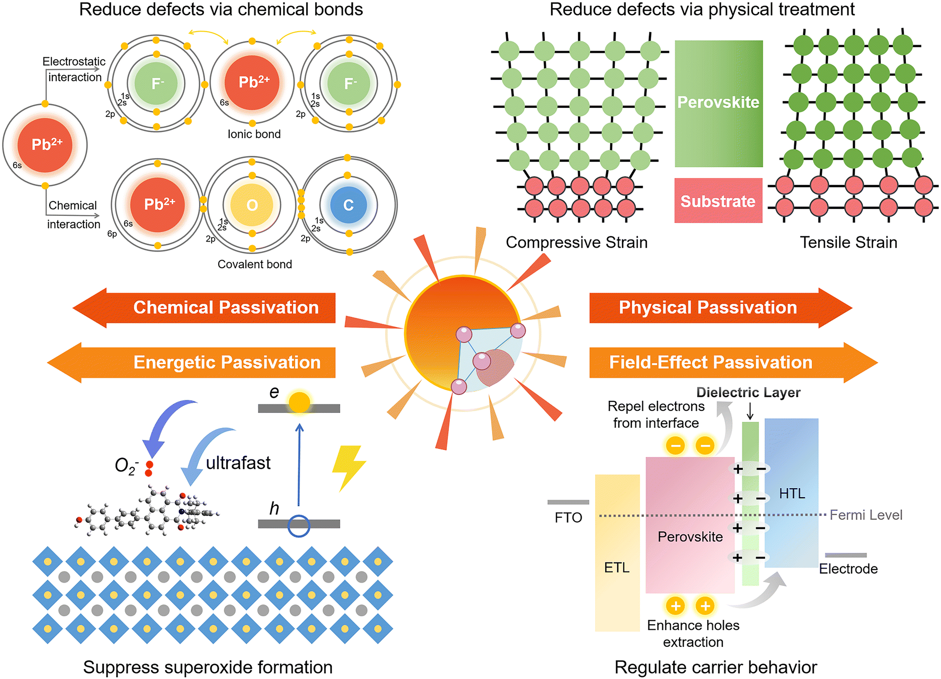 | ||
| Fig. 1 Passivation strategies toward high-efficiency and stable PSCs and their functions, including chemical passivation, physical passivation, energetic passivation, and field-effect passivation. | ||
Aside from these traditional means for defect reduction, another strategy called ‘energetic passivation’ was recently proposed by Gao and Long's groups, endeavouring to prevent the perovskite layer from being attacked by excited oxygen during the operation under light (improving the light/oxygen stability of the absorber) (Fig. 1).22,23 The mechanism of energetic passivation is defined as the introduction of midgap states created by the passivator to capture the photoexcited electrons prior to oxygen to avoid the generation of superoxide anion radicals in the photo-excited perovskites. Active superoxide radical is known to trigger the degradation of the hybrid perovskite layer by reacting with organic cations when exposed to both light and oxygen, severely impairing the lifetime of PSCs.24 Inspired by the advancement in silicon solar cells, field-effect passivation has been successfully applied in PSCs recently.25 By inserting a dielectric layer (with a strong dipole or high work function) at the interface of the perovskite absorber and transport layer, the resultant interfacial band-bending shields photo-generated charge carriers from recombination active regions by repelling or separating free charges (either electrons or holes) from the interface, decreasing the probability of charge trapping at defect sites and minority carrier recombination at the interface (Fig. 1). This benign behavior boosts valid charge transfer, alleviates carrier accumulation, decreases the recombination velocity, and improves the photovoltaic performance of PSCs.
This review presents a brand-new rationalization of passivation strategies for PSCs in recent years, including chemical, physical, energetic, and field-effect passivation, highlighting their significance and uniqueness. Besides the comprehensive review of the most recent passivation strategies, the identification and direct observation of passivation effects in perovskites are summarized based on the corresponding advanced characterization techniques, which are equally crucial for the purpose of ‘suiting the remedy to the case’. Finally, we offer a guideline for further development by looking at the challenges and opportunities for these four types of passivation strategies.
2. Passivation strategies of perovskite solar cells
2.1 Chemical passivation
Applying certain chemicals to react with defect sites via constructing chemical bonds (covalent bonds, ionic bonds) on the surface or from the bulk of perovskite materials for deactivating their electronic or chemical reactivities is the main function of chemical passivation, which has been extensively studied over the past decade.26,27 Covalent bonds can be understood as the interaction between two atoms by sharing electrons. In contrast, ionic bonds are formed between a positively charged cation and a negatively charged anion through electrostatic interaction. Besides, intermolecular non-covalent interaction, including halogen bonding and hydrogen bonding that belong to the electrostatic force of attraction, can also reduce the defects of perovskite materials. Passivation by halogen bonding aims for electron-rich defects (negatively charged defects),28–30 while passivation by hydrogen bonding can deal with both positively and negatively charged defects.31,32 These beneficial intermolecular interactions are often accompanied by the construction of chemical bonds between the passivators and defect sites, further enhancing the effects of chemical passivation.As an imperative implement towards high device performance, chemical passivation that can directly eliminate defects has been commonly utilized not only in most reported PCSs (Table 1), but also in perovskite-based light-emitting diodes and photodetectors.33,34 Generally, defects derived from the film surface are more notorious than those generated from the film interior as interface trap density is several orders of magnitude higher than that in the bulk, resulting in more attention being paid to interface engineering than additive engineering.10 Although chemical passivation strategies have been discussed in quite a few review works as part of interface engineering or additive engineering,7,10,17,35 no thorough review has been performed from the perspective of the nature of chemical passivation so far. More importantly, significant breakthroughs have been made in chemical passivation in the past three years, yielding many noteworthy signs of progress that deserve summarization and prospect, which are the critical points to be discussed in this part.
Lewis-acid passivator refers to a molecule that can accept nonbonding electrons, thereby enabling the passivation of electron-rich defects in perovskites. The most common examples are fullerene (C60) and its derivatives ([6,6]-phenyl-C61-butyric acid methyl ester (PCBM), etc.), which have outstanding electron accepting capability and high chemical reactivity. Moreover, the shape of this class of substances can be modified by accepting an electron and thus drastically reducing the intrinsic strain of the molecule, leading to an excellent passivation effect.36 PCBM, commonly deposited on the perovskite film as the electron transport layer (ETL), was observed to effectively passivate charge trap states and eliminate the photocurrent hysteresis of PSCs.37 The theoretical calculation results show that PCBM thermodynamically favors interaction with halide-rich defects at the surface or grain boundaries while showing hybridization with the surface, which is in agreement with the passivation mechanisms of Lewis acid.38 It is worth mentioning that the in-depth mechanisms behind the C60 or its derivative passivated perovskites should be further resolved.
In addition, Lewis acids with the structure of fluorine-substituted aromatic rings connected to a III–V element were also employed to provide chemical passivation for under-coordinated halide anions.39,40 Iodopentafluorobenzene (IPFB) is the first investigated Lewis acid with this structure that passivates under-coordinated halide defects by forming halogen bonding (non-covalent bond).28 Furthermore, based on the structure of IPFB, a modified Lewis acid named tris(pentafluorophenyl) phosphine (TPFP) was developed.39 In the molecular architecture of TPFP, every fluorine-substituted benzene ring has a similar structure to IPFB. However, a stronger positive charge center is formed at the centered phosphorus atom due to fifteen strongly electronegative fluorine atoms.39 Therefore, Lewis acids of this type can function as a good electron acceptor that accepts an electron from under-coordinated I− and IPb antisite defects through Lewis acid–base adduction interaction,39,40 instead of forming halogen bonding with under-coordinated halide defects like IPFB. The strong electronegativity of fluorine atoms also can produce hydrophobicity to enhance the moisture stability of devices. However, research on Lewis-acid type passivators is limited to a few types, and more efforts should be made to broaden the choice to achieve more efficient passivation for certain pernicious electron-rich defects.
Lewis-base passivators are defined as organic compounds with lone-pair donating end groups, such as carbonyl (C![[double bond, length as m-dash]](https://www.rsc.org/images/entities/char_e001.gif) O), sulfoxide (SO), phosphate (PO), and cyano (C
O), sulfoxide (SO), phosphate (PO), and cyano (C![[triple bond, length as m-dash]](https://www.rsc.org/images/entities/char_e002.gif) N) groups. In some cases, these nonbonding electron pairs were found to coordinate with undercoordinated Pb2+/PbI antisite and passivate lead clusters.41,42 The simplest Lewis bases applied for passivating perovskites are thiophene and pyridine, on which the nitrogen atom (in pyridine) or the sulfur atom (in thiophene) provides additional electron pairs for under-coordinated Pb2+ and facilitates the reduction of non-radiative recombination in perovskites.43,44 Liu et al. further revealed the different passivation mechanisms of pyridine and thiophene by non-adiabatic (NA) molecular dynamics combining time-domain density functional theory (TD-DFT).45 Thiophene removes electron density from the surface, while pyridine attracts electrons at the surface into an unoccupied orbital localized around the coordinative bond formed by the pyridine nitrogen and under-coordinated Pb2+ on the surface. As a result, both molecules reduced the NA coupling and extended the non-radiative recombination time by an order of magnitude. Since then, a large number of Lewis base-containing passivators have been developed for defect passivation in PSCs as represented by 1,1-dicyanomethylene-3-indanone (π-conjugated Lewis base),46,47 urea (small molecule),48–50 poly(vinyl acetate) (PVA, polymer),51etc.
N) groups. In some cases, these nonbonding electron pairs were found to coordinate with undercoordinated Pb2+/PbI antisite and passivate lead clusters.41,42 The simplest Lewis bases applied for passivating perovskites are thiophene and pyridine, on which the nitrogen atom (in pyridine) or the sulfur atom (in thiophene) provides additional electron pairs for under-coordinated Pb2+ and facilitates the reduction of non-radiative recombination in perovskites.43,44 Liu et al. further revealed the different passivation mechanisms of pyridine and thiophene by non-adiabatic (NA) molecular dynamics combining time-domain density functional theory (TD-DFT).45 Thiophene removes electron density from the surface, while pyridine attracts electrons at the surface into an unoccupied orbital localized around the coordinative bond formed by the pyridine nitrogen and under-coordinated Pb2+ on the surface. As a result, both molecules reduced the NA coupling and extended the non-radiative recombination time by an order of magnitude. Since then, a large number of Lewis base-containing passivators have been developed for defect passivation in PSCs as represented by 1,1-dicyanomethylene-3-indanone (π-conjugated Lewis base),46,47 urea (small molecule),48–50 poly(vinyl acetate) (PVA, polymer),51etc.
Nevertheless, the distributions and compositions of defects of the perovskite films are very complicated. In the actual situation, the positively and negatively charged defects appear concurrently and distribute away from each other with an uncertain molar ratio. This can be explained because the perovskite film surface does not necessarily reach thermal dynamic stable states right after the annealing step, and the surface defects may pair up with bulk defects.14 Therefore, in practice, the passivation effect of single-function Lewis acid only for negatively charged defects or Lewis base only for positively charged defects may be limited. The dual passivation of both types of charged defects by Lewis acid/base to surmount the complicated defect composition or distribution can be achieved using two strategies: (1) applying a Lewis acid and a Lewis base simultaneously.52 Zhu et al. combined bis-PCBM mixed isomers (Lewis acid) in antisolvent and N-(4-bromophenyl)thiourea (BrPh-ThR) (Lewis base) in perovskite solution precursor, intending to passivate both negatively and positively charged defects during the fabrication process of perovskite films (Fig. 2a).52 This direct combination of Lewis acid and base enabled marked passivation of under-coordinated Pb2+ and IPb antisite defects, which improved device efficiency from 19.3% to 21.7%. (2) Lewis acid/base integrated molecules (zwitterionic molecules) with spatially separated electronegative and positive regions with the advantage of a self-adaptive selection of defects for opposite charged defects for passivation. This conception has been achieved by combining Lewis-base groups and protonated functional groups (such as –OH and –NH) in one molecule.23,42,53 From the electrostatic potential surface (EPS) of such passivators (Fig. 2b), the Lewis-base and protonated groups formed a push–pull electronic structure, in which the unbalanced electron distribution constituted the functional sites for the efficient passivation of both negatively and positively charged defects, contrasting the monofunctional Lewis-base system (Fig. 2c).23
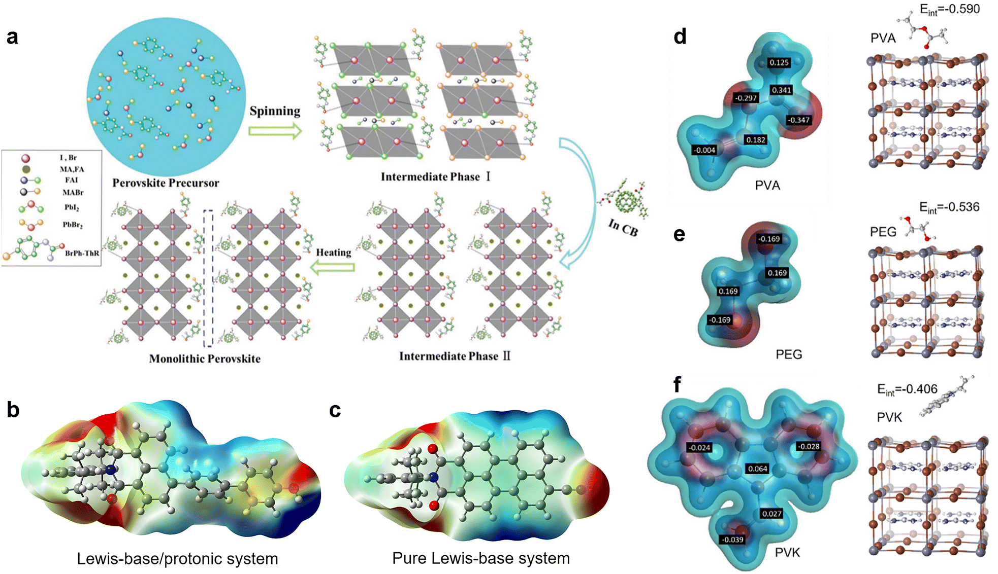 | ||
| Fig. 2 (a) Schematic reaction process of perovskite growth resulting from the combination of the Lewis base BrPh-ThR in the perovskite-solution precursor and the Lewis acid bis-PCBM in the antisolvent process. Reproduced from ref. 52 with permission from the Royal Society of Chemistry, copyright 2018. Passivator with (b) Lewis-base/protonated system and (c) pure Lewis-base system. Reproduced from ref. 23 with permission from Wiley-VCH, copyright 2021. (d–f) The partial charge distribution of PVA, PEG, and PVK and the interaction energies of their monomers to interact with the surface iodide vacancy defect of perovskite crystals. Reproduced from ref. 51 with permission from Elsevier, copyright 2022. | ||
The synergistic passivation effects of the second strategy have been reported by several groups. Yang et al. proposed that when –NH and CO groups were constructed in an optimal configuration in a molecule, the –NH groups could interact with I− in the PbI64− octahedron through hydrogen bonds, facilitating the binding of CO with the PbI antisite to give a maximized passivation effect.42 Later, Gao's group demonstrated that Lewis bases accompanied by protonated functional groups have stronger chemical passivation ability than only Lewis base groups. The superiority of 4-hydroxybiphenyl substituted NMI (4OH-NMI) with both CO and protonated –OH groups originated from the additional capability of the protonated group to deal with negatively charged defects.23 Very recently, benefiting from the synergistic effects of the Lewis-base/protonated system (CO/–NH) of the Indigo compounds, Yuan et al. achieved efficient chemical passivation of under-coordinated Pb2+/I− and PbI antisite defects, as well as improved device stability under heat and moisture stresses.53 Therefore, combining Lewis-base and protonated groups in one passivator following a judicious design is of great significance in achieving efficient chemical passivation.44
The passivation effect of the Lewis bases is very relevant to their molecular structures. However, most studies focused on simply changing the functional groups, and less attention has been paid to the influence of structure on the interaction stability between the perovskite and passivators. This could be due to the fact that finding an optimal molecular structure for the Lewis acid/base passivator generally involves tedious trial-and-error procedures. Despite the difficulty, Li et al. investigated the stability of the passivation effect of Lewis-base passivators by analyzing the coordination interactions between Lewis-base groups and positively charged defects that can be easily damaged under the erosion of the external environment.54 They demonstrated that surface molecule superstructure, such as dimer and even periodic close-packed interconnected structure of tribenzylphosphine oxide (TBPO), enabled by π–π self-assembly, contributed to the improved stability of the coordination interactions between Lewis-base groups and positively charged defects.
Lately, to elaborate on the relationship between the defect passivation capability of polymeric passivators and their molecular structure, Yang et al. calculated the partial charge distribution of three polymers, including poly(vinyl acetate) (PVA), polyethylene glycol (PEG), and poly(9-vinylcarbazole) (PVK), as well as the interaction energies between their monomers and iodide vacancy on the surface of perovskite crystals (Fig. 2d–f).51 They found that the difference in the interaction energies is attributed to the varying strength of the partial charge and degree of steric hindrance of the interacting functional groups. For example, the greater negative partial charge of the ester groups (CO, Lewis-base groups) on the side chain of the PVA monomer enabled more accessibility to the undercoordinated Pb2+ (iodide vacancy). In contrast, the smaller partial charge of the ether bond (C–O) on the PEG (hindered by surrounding CH2) and the partial negative charge of the bulky carbazole group on the PVK limited their interaction with the defects, delivering lower interaction energies. Fourier transform infrared (FTIR) spectroscopy, and X-ray photoelectron spectroscopy (XPS) further confirmed these simulation results. Consequently, PVA gave the most excellent passivation effect for charged defects and achieved a remarkably improved PCE of 23.2%.
As an emerging passivation strategy, the host–guest complexations exerted by crown ethers (or their ion-accepting molecules) have shown a marked passivation effect for positively charged defects (undercoordinated Pb2+, FA+, and Cs+) of perovskites through the formation of coordination/hydrogen bonds.55,56 Crown ethers are well-known cyclic etheric molecules, possessing highly electronegative cavities that can selectively chelate different cations. Their selectivity is based on the size of the ring structure. Thus, the coordination between crown ethers and positively charged defects can be classified into Lewis acid–base adduction interaction. Grätzel et al. were the first to employ crown ethers to passivate the undercoordinated surface defects.55 The interaction between crown ethers and defects, namely host–guest complexations, was elucidated by solid-state nuclear magnetic resonance and density functional theory (DFT) calculations. Their results showed that crown ether is not just adsorbed but reacts with the perovskite film via coordination between the oxygen atoms and positively charged defects on the perovskite surface. Consequently, they achieved PSCs with substantially improved efficiency exceeding 23% and enhanced operational stability. Later, the same group further applied a modified crown ether, dibenzo-21-crown-7, to act as a vehicle that assembles at the interface and delivers Cs+ ions into the interior.56 This host–guest complexation strategy provided a local nanoscale gradient of Cs+ that facilitates photo-induced charge separation while passivating positively charged defects, leading to exceeding 24% efficiency devices with improved stability.
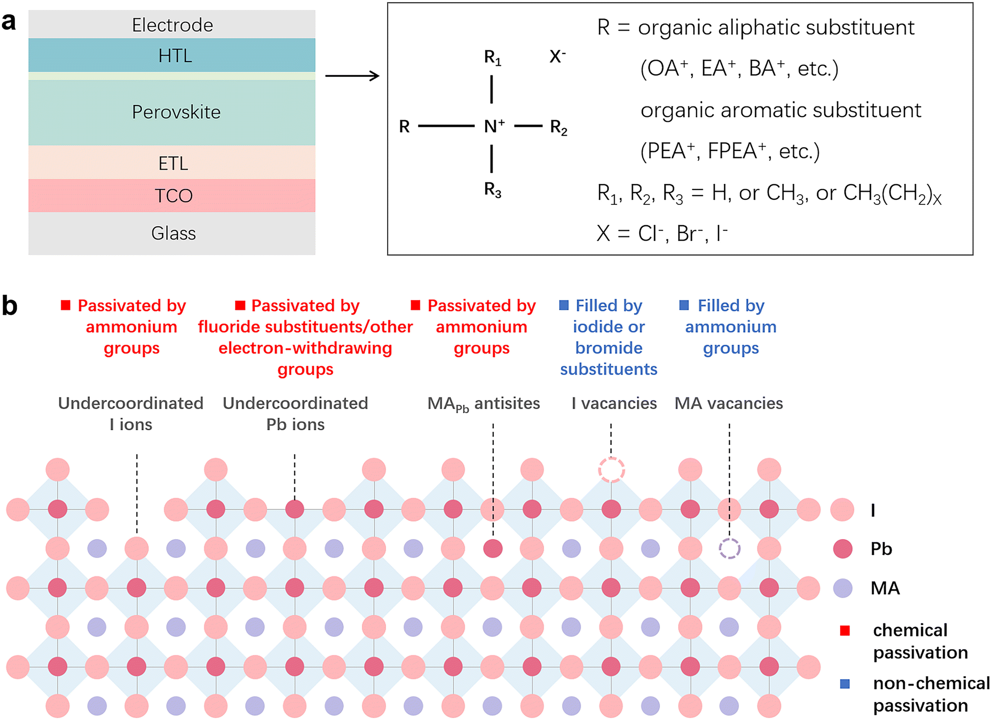 | ||
| Fig. 3 (a) The general formula for ammonium halide salts with the typical n–i–p structure of PSCs. (b) Schematic diagram of defect types in MAPbI3 perovskites and the corresponding passivation effects of ammonium halide salts which are divided into chemical and non-chemical passivation. | ||
Similar to zwitterionic molecules, the structure tunability of ammonium halide salts endows them with multiple passivation abilities to cope with several different types of defects on the surface or in the bulk of perovskites. As illustrated in Fig. 3b, the comprehensive passivation effect of ammonium halide salts comes from the following points: (a) ammonium groups heal the negatively charged defects by electrostatic interactions (ionic bonds);72 (b) ammonium groups reduce organic cation vacancies by occupying the corresponding sites;14 (c) ammonium groups passivate substitutional defects like MAPb defects by attracting one iodine atom to break the I-dimer;73 (d) iodide and bromide substituents fill the halide vacancies of perovskites;74 (e) fluoride substituents in the halide site with the strong electronegativity form robust ionic bonds with Pb-related defects and hydrogen bonds with organic cations;75,76 (f) interstitial chlorine ions restore the tilting octahedra induced by the MA interstitial defect via Coulomb interaction with lattice Pb2+ ions;74 and (g) additionally, if the ammonium halide salts are attached to electron-withdrawing groups, they will have the ability to passivate positively charged defects.72 Among these abilities, (a), (c), (e) and (g) belong to the chemical passivation effect. Combining the excellent chemical passivation ability for the charged defects, the capability of vacancy filling, and the formed low-dimensional perovskite overlayer, ammonium halide salts can efficaciously enable suppressed ionic migration and decreased defect-assisted recombination in the passivated PSCs, giving significant efficiency enhancement and stability improvement. Although the chemical passivation effects in ammonium halide salts have been mentioned frequently in previous works, there are a few studies on the differentiation and optimization of their passivation ability, which may originate from the inherent complexity and the more conspicuous merits of low-dimensional perovskites that distracted the attention of the researchers and led to the insufficient understanding of the chemical passivation process.63,77,78
It is known that the electronic band structure of perovskite materials is determined by the frontier orbitals of the divalent cation and halide.91,92 Hence, incorporating monovalent alkali metal cations (K+, Na+, Rb+, and Cs+) into perovskites usually does not affect the bonding directly and shows only passivation effects. Bi et al. found that Na+ ions can diffuse into grain boundaries over time, enabling lower defect density and improved photoluminescence (PL) lifetimes.81 They proposed that Na+ ions potentially passivate the negatively charged defects by forming ionic bonds with undercoordinated halides and reduce vacancy defects by filling the MA vacancies owing to their similar size and isovalent charge with MA+. Similarly, K+ ions were found to accumulate at grain boundaries on the film surface and form ionic bonds with the halides to passivate both undercoordinated Br− and I−.82 (Fig. 4a) The K+ ions also play a role in mixed-cation PSCs to eliminate photocurrent hysteresis due to the lower formation energy of the K interstitial and suppressed ion migration.83 Rb+ ions have homologous but weaker passivation ability than K+ ions, which can be explained by the worse solubility of the non-perovskite phase (Rb–I–Br-based phase) in the Rb-doped device than the K-doped case (KBr), causing adverse effects on device performance.93 Recently, theoretical calculations by Long and his co-workers revealed that alkali metal cations with negative doping energy could get easily inserted into the interstitial sites of the perovskite lattice and increase the formation energy of iodine interstitial while decreasing the defect concentration (Fig. 4b). If the defects are already present, the alkalis bind strongly to them through electrostatic interactions, eliminating the midgap state that traps charge carriers and diminishing the trap-assisted non-radiative recombination energy loss.94 Another theoretical calculation work showed that small alkali metal ions like K+ ions with a radius of 1.38 Å are energetically favorable to occupy the interstitial sites within the perovskite lattice. These filled interstitial sites can prevent the formation of iodide Frenkel defects and hinder ion migration, leading to a similar passivation effect to ionic bonding at the surface/grain boundaries and hysteresis-free PSCs.83
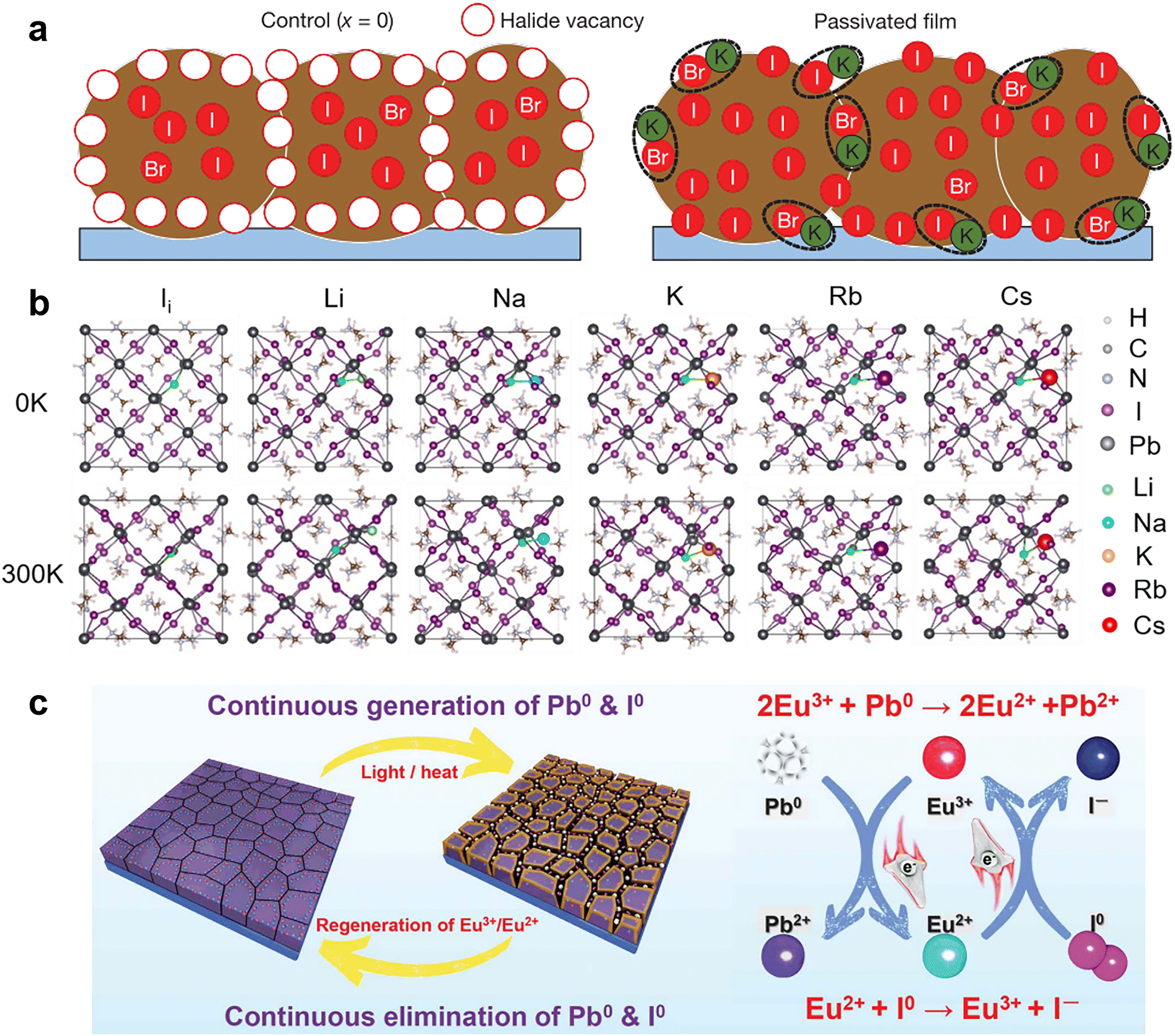 | ||
| Fig. 4 (a) Schematic of a cross-section of a film showing halide-vacancy management in the case of excess halide, in which surplus halide is immobilized through complexing with potassium into benign compounds at the grain boundaries and surfaces. Reproduced from ref. 82 with permission from Springer Nature, copyright 2018. (b) Structures of pristine, Li doped, Na doped, K doped, Rb doped, and Cs doped iodine interstitial systems formed by introducing an alkali atom into iodine interstitial MAPbI3. Reproduced from ref. 94 with permission from Wiley-VCH, copyright 2020. (c) Proposed mechanism diagram of cyclical elimination of Pb0 and I0 and regeneration of Eu3+–Eu2+ metal ion pair. Reproduced from ref. 80 with permission from Springer Nature, copyright 2019. | ||
For the same reason mentioned above,91,92 the applications of divalent metal cations are more inclined to be incorporated into the perovskite crystal lattice to replace lead ions at the B-site.88 However, due to the strict atomic size and electronic structure requirement, only a tiny fraction of divalent metal cations work as chemical passivation. For instance, in the two-step sequential deposition of perovskite films, the incorporation of Ni2+ into the interstices of the PbI2 lattice led to an electron interaction between Ni2+ with MA+ and octahedral [PbI6]4−, thus restraining the formation of IPb defects. Meanwhile, the configuration of Ni2+ ions that was mainly distributed among the inorganic cages composed of MA+ and octahedral [PbI6]4− induced an ordered arrangement of MA+ and reduced the undercoordinated halides via coordinate bonds. Another divalent metal cation, Cd2+, was demonstrated to assist crystal growth and passivate negatively charged defects through ionic interactions.89 The rare-earth metal cation, Eu3+/Eu2+, was revealed to act as a “redox shuttle” that selectively oxidizes Pb0 (generated by the reduction of Pb2+) and reduces I0 defects (produced by the easy oxidization of I−) through electron transfer in the following two chemical reactions: 2Eu3+ + Pb0 → 2Eu2+ + Pb2+ and Eu2+ + I0 → Eu3+ + I− (Fig. 4c).80 As a result, Eu3+-incorporated PSCs gave improved efficiency and long-term durability.
2.2 Physical passivation
Physical passivation, including strain relaxation, thermal annealing treatment, and surface polishing, is another strategy to reduce the defects of perovskite materials from a physical perspective. Unlike straightforward chemical passivation, physical passivation is not limited by perovskite compositions and device configurations. It could avoid adding potentially detrimental chemical reagents to the components of the device but take effects via subsequent internal chemical transformations. More importantly, most of the physical passivation strategies are timely and effective enough to be compatible with the scaling up of perovskite solar cells and modules.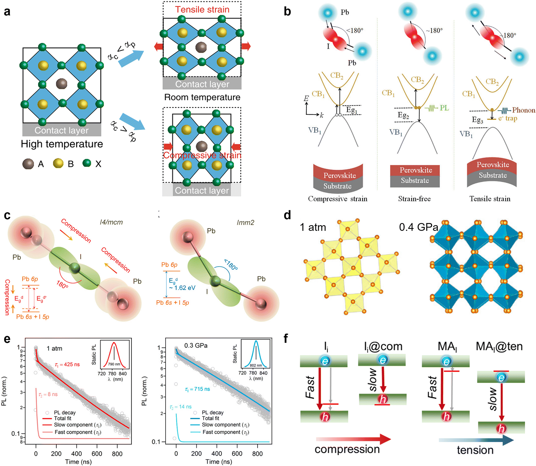 | ||
| Fig. 5 (a) Schematic illustration of the formation of tensile and compressive strains. Reproduced from ref. 19 with permission from Springer Nature, copyright 2020. (b) Schematic illustrations of various recombination mechanisms and bandgap evolution in MHPs. The relation Eg1 < Eg2 < Eg3 results from the generated strains/stresses. Reproduced from ref. 99 with permission from Wiley-VCH, copyright 2021. (c) Schematic models for the changes of the Pb–I–Pb bond angle with the strain increasing of the I4/mcm and Imm2 phases; (d) Pb–I inorganic frameworks of MAPbI3 at 1 atm and 0.4 GPa; (e) TRPL measurements on a MAPbI3 single crystal at 1 atm and 0.3 GPa. Reproduced from ref. 101 with permission from the National Academy of Sciences, copyright 2016. (f) Schematic illustration of the tensile and compressive strain shifting traps from bandgap into bands. Reproduced from ref. 47 with permission from American Chemical Society, copyright 2021. | ||
Furthermore, it is found that the strain can cause a phase transformation of perovskites. Without introducing any adverse chemical or thermal effect, Kong et al. applied a hydrostatic strain to precisely modulate the crystal lattice of perovskites.101 They found that the strain drives the I4/mcm phase transit to the Imm2 phase of MAPbI3, which is a crucial factor in altering the electron-density function between Pb and I atoms via the change of bond angles (Fig. 5c and d). More importantly, the mild strain of ∼0.3 Gpa simultaneously narrows the bandgap and prolongs the carrier lifetime of perovskites (Fig. 5e), which implies its ability to reduce defect densities and is a desirable trend for achieving better device performance. Then, Zhu et al. demonstrated that the efficiency of PSCs can be enhanced up to 20.7% by reducing the strain gradient of FAPbI3.102 From the first-principles calculations, they found that the tensile strain can cause perovskite valence band bending that improves hole transport and extraction.
Based on the simulation, Long and his co-workers recently revealed the mechanism underlying the enhanced performance by strain application for PSCs from the defect passivation perspective.47 The compressive and tensile strain can drive the trap states introduced by iodine interstitial (Ii) and substitution of iodine with methylamine (MAI) merging into band edge and mitigate their negative effect that serves as recombination centers. In detail, the compressive strain enhances the coupling of Pb-s and I-p and pushes up the valence band maximum (VBM), while the increased Pb–Pb distance under the tensile strain weakens the overlap of Pb-p orbitals and pushes down the conduction band minimum (CBM). Consequently, the trap states caused by Ii near the VBM and MAI close to CBM can be shifted into bands and no longer create midgap charge recombination centers under strain, efficiently suppressing the non-radiative recombination process (Fig. 5f). However, these defects physically passivated by strain also perturb the pristine system and introduce modest disorder that reduces delocalization of electron and hole wave functions and decreases their overlap. In addition, the compressive and tensile strains both generate less charge overlap and smaller NA coupling, hence a significantly longer carrier lifetime. This impressive work highlights the role of defect passivation in strain relaxation and the significance of defect characterization for its experimental studies in the future.
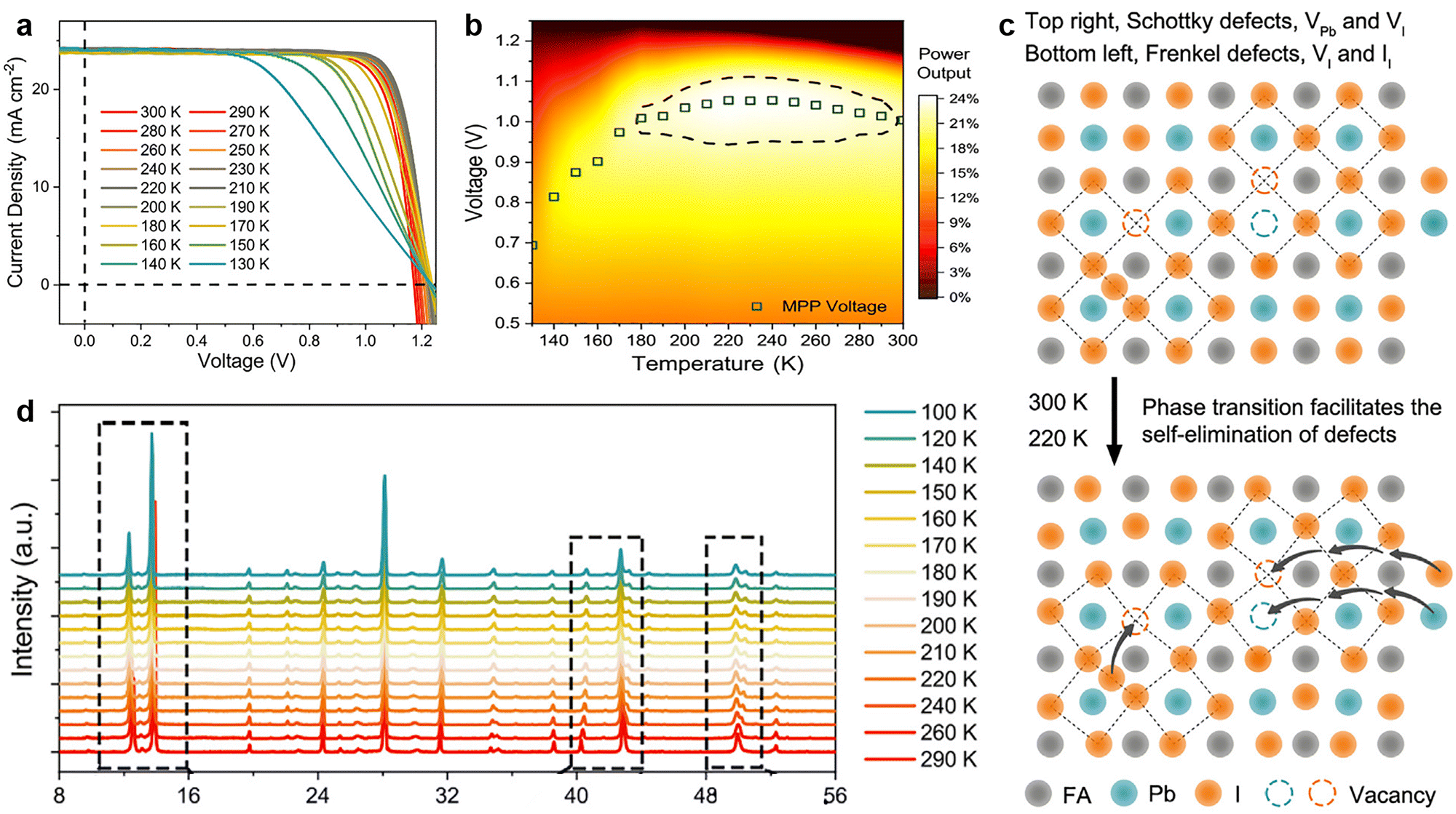 | ||
| Fig. 6 (a) J–V curves of the FAMAC-based PSCs at different temperatures from 300 to 130 K, with a step of 10 K; (b) temperature and applied voltage-dependent power output plot of PSCs. (c) A schematic illustration for the self-elimination of intrinsic defects via phase transition; (d) XRD patterns as a function of the temperature from 290 to 100 K for FAMAC-based perovskite film. Reproduced from ref. 20 with permission from Elsevier, copyright 2020. | ||
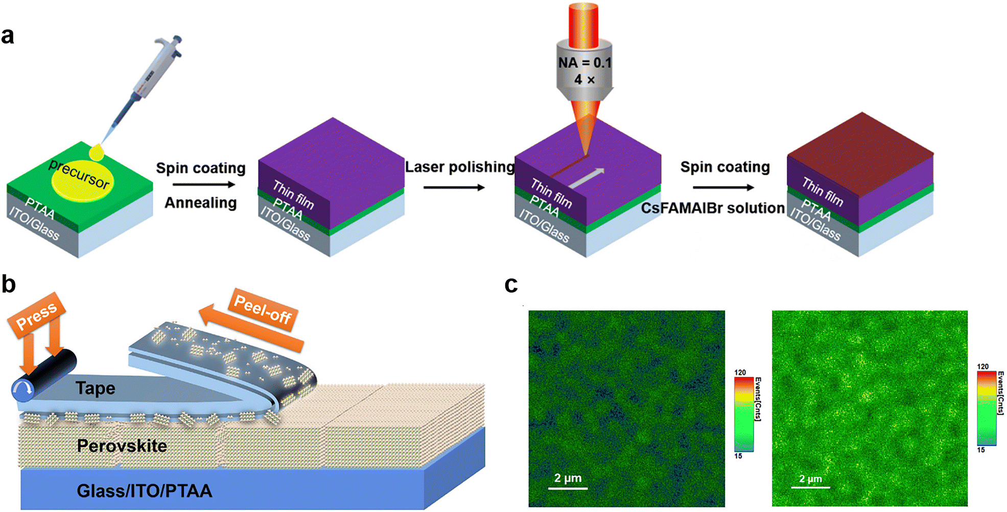 | ||
| Fig. 7 (a) The scheme of PSC fabrication processing with fs-laser polishing. Reproduced from ref. 21 with permission from Wiley-VCH, copyright 2020. (b) Schematic of peeling an adhesive tape off the perovskite film; (c) PL mapping images of perovskite film before (left) and after (right) tape treatment. Reproduced from ref. 105 with permission from Elsevier, copyright 2020. | ||
However, the current polishing strategy by lasers is suitable for PSCs with small areas but hard to be applied to the scalable, high-speed manufacturing of large-area perovskite photovoltaic modules, especially for devices fabricated by a roll-to-roll process requiring substrate flatness and absorber thickness. To achieve efficient physical passivation with low-cost and high-throughput processability for large-area cells and modules, Huang and co-workers designed a facile method that utilized low-cost adhesive tapes to mechanically polish the polycrystalline films to remove defects, such as amorphous phase and excessive PbI2 particles that cause the degradation of perovskites via the photolysis effect.105 The application of adhesive tape made of soft adhesive on a flexible polymer substrate is shown in Fig. 7b. The tape is pressed onto the rough and defective perovskite surfaces to form an intimate contact with appropriate bonding strength. After peeling off this adhesive tape, the amorphous phase can be retained on the tape and thereby removed from perovskite films. The thermal admittance spectroscopy (TAS) measurement revealed that the polished film exhibited a much lower shallow-level defect density of states in the shallow trap depth region, attributed to the removal of defective surfaces. This result was supported by the enhanced PL intensity after tape treatment, suggesting suppressed non-radiative recombination (Fig. 7c). Even more interesting is that a thin layer of polymer adhesive on top of perovskite films left by the tape can also have chemical passivation effects on devices. Finally, the tape-treated MAPbI3 PSC exhibited improved efficiency of up to 22.0% with a long operational time of over 1400 h without efficiency loss. This mechanical polishing strategy is expected to work on other commonly used perovskite compositions and is desired for the scaling up of perovskite photovoltaics.
2.3 Energetic passivation
It is widely known that neutral oxygen molecules have little impact on perovskite stability, as they interact weakly with perovskites.106 Nevertheless, oxygen molecules can diffuse into the perovskite lattice at a fast rate. When exposed to light and oxygen, the oxygen molecules accept the photoexcited electron from the perovskite under light to form superoxide (O2−) (Fig. 8a).16,107,108 The reactive superoxide radical will deprotonate the organic methylammonium cation of photo-excited halide perovskites and break the inorganic Pb–I bonds, leading to the formation of PbI2, water, methylamine, and iodine, thereby severely impairing the operation stability of PSCs.16,24 More seriously, this degradation can be accelerated further when the superoxide radical is further reduced to peroxide (O22−) since the doubly negative charge of O22− repulses I− and attracts Pb2+ more strongly.106 Superoxide-induced degradation also occurs in mixed-cation perovskites due to their organic components.109 Moreover, light and oxygen-induced degradation has been proven to occur faster than the more widely studied moisture-induced degradation.110 Hence, suppressing the formation of superoxide is crucial to improving the stability of perovskite toward light and oxygen.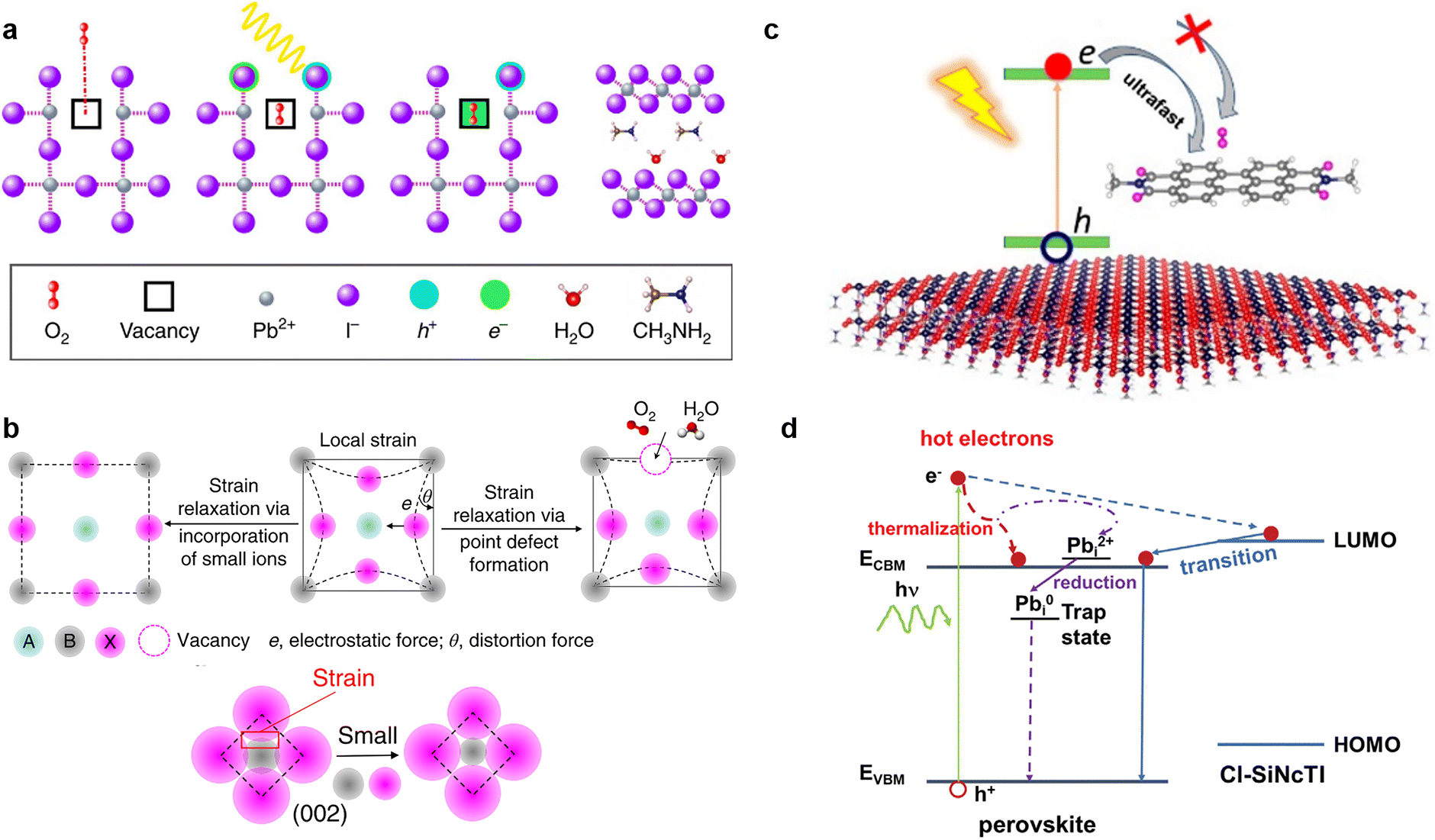 | ||
| Fig. 8 (a) Oxygen-induced photo-degradation. Schematic representation of the reaction steps of O2 with MAPbI3, including oxygen diffusion and incorporation into the lattice; photoexcitation of MAPbI3 to create electrons and holes; superoxide formation from O2; reaction and degradation to layered PbI2, H2O, I2, and MA+ (from left to right). Reproduced from ref. 16 with permission from Springer Nature, copyright 2017. (b) Schematically illustrating that the local strain can be reduced by forming point defects or incorporating small ions, and the distortion angle decreases via strain relaxation. Reproduced from ref. 113 with permission from Springer Nature, copyright 2018. (c) Midgap states created by passivators are higher than the trap states generated by O2, favoring the capture of photoexcited electrons of the perovskite and suppressing superoxide formation. Reproduced from ref. 22 with permission from American Chemical Society, copyright 2021. (d) Photo-excited carrier dynamics in an energy-space diagram. Reproduced from ref. 116 with permission from Wiley-VCH, copyright 2022. | ||
According to previous reports, the trap states of iodide vacancies are in the bandgap of perovskites, and they are most energetically favorable for forming superoxide when occupied by a trapped electron.16 Traditional chemical passivation strategies can be used to lessen the iodide vacancies inside the perovskite film, such as directly introducing ammonium iodide (MAI or PEAI),111 to fill the vacancy and alleviate the formation of in-bandgap trap states. Meanwhile, some zwitterionic molecules, such as amino valeric acid (AVA), can bind to the iodide vacancies and prevent oxygen from accessing, so as to protect perovskites from superoxide-induced degradation.112 Physical passivation strategy could also be used. It was reported that judiciously selected metal cations such as cadmium could be incorporated into a mixed perovskite lattice to release the remaining lattice strain, further increasing the formation energy of iodide vacancies (Fig. 8b).113
Nowadays, some novel methods are introduced to achieve the same purpose. (1) Neutral oxygen is found to be able to passivate iodide vacancies by separating the localized charge density and weakening the electron–phonon interaction.114 (2) Inserting an electron acceptor layer with a proper frontier orbital level between the ETL and perovskite absorber to improve electron extraction from the perovskite absorber before they can react with oxygen.110 (3) Doping alkaline-earth metal into perovskites to eliminate superoxide. A theoretical study by Long et al. suggested that these metal atoms can break the O–O chemical bond and shift the O–O antibonding orbitals located inside the bandgap into the bands.115
However, small oxygen molecules can still penetrate the interlayers through the pores and form superoxide by accepting an electron through the midgap states from the photoexcitation perovskite.106 At present, although encapsulation for PSCs is usually used to cut off oxygen, there is still a tiny amount of residual oxygen in the space of the device after encapsulation. In this context, the advantage of the energetic passivation strategy in holding back the superoxide generation became visible. The passivator introduced for this purpose can create benign midgap states for the excited perovskite that capture the photoexcited electrons prior to oxygen to avoid the generation of superoxide anions.22,23
Using nonadiabatic molecule dynamics simulations, Long and his coworkers found that an electron-accepting molecule (e.g., perylene diimide (PDI)) with electronic levels higher than the oxygen-created midgap states inside the perovskite bandgap can restrain superoxide-induce degradation22 (Fig. 8c). The midgap state created by PDI can rapidly capture the photo-generated electron of perovskite at about 100 ps before the O2-related trap state, which takes about double the time. The fast electron trapping originates from the strong NA coupling and small energy gap between the PDI midgap state and the MAPbI3 CBM. This simulation suggests that a rational design of an electron-accepting conjugated molecule with suitable molecular orbitals of the polyaromatic imide compounds has the potential to achieve the energetic passivation effect.
Inspired by the above study, our group revealed two passivators, i.e., 4OH-NMI with a Lewis-base/polyaromatic/protonated system and cyanide-substituted perylene-3,4-dicarboximide (9CN-PMI) with Lewis-base/polyaromatic/Lewis-base system, have different degrees of ability for energetic passivation.23 Both 4OH-NMI and 9CN-PMI can create benign midgap states above the trap states produced by O2 to capture the photoexcited electrons on perovskite prior to oxygen, thereby avoiding the formation of superoxide anions. However, the midgap states created by 4OH-NMI are much closer to the conduction CBM of perovskite than that of 9CN-PMI and exhibit stronger non-adiabatic electron–phonon coupling, which enables faster electron trapping and thus a stronger energetic passivation effect. Moreover, the slightly wider bandgap of 1.45 eV for the 4OH-NMI-passivated system than that of the 9CN-PMI-passivated system (1.42 eV) suggests a more negligible non-adiabatic coupling that favors slower non-radiative recombination loss. Benefiting from the excellent energetic passivation and the chemical passivation effects of 4OH-NMI, a high-performance PSC with an efficiency of 23.7% and improved light/oxygen stability was achieved. This work reveals that the more the passivator-generated midgap states are close to the CBM of perovskite materials, the faster the passivator captures the photoexcited electrons.
Our group recently proposed a novel energetic passivation strategy using ambipolar silicon naphthalocyanine tetraimides (Cl-SiNcTI) via a simple antisolvent-assisted crystallization method.116 The suitable molecular orbital of Cl-SiNcTI enables a high-lying band above the conduction band of the perovskite, which can compete for high-energy photocarriers. This beneficial behavior not only facilitates the collection and thermalization of hot carriers to suppress the formation of Pb2+ to Pb0 to reduce Fermi-level pinning, but also inhibits the formation of superoxide from the reaction between oxygen molecules and photoexcited electrons (Fig. 8d). The consequent champion device exhibited a high VOC of up to 1.18 V and an enhanced PCE of 23.5% due to the decreased trap-assisted recombination, as well as improved photo-oxygen stability.
As shown from the above examples, if the organic molecules have appropriate electronegativity to accept or donate pair of nonbonding electrons for defects of perovskites, they also provide functions of chemical passivation to improve device efficiency and stability (defect-related). Undoubtedly, energetic passivation can be the last frontier for perovskites against the degradation induced by light and oxygen, which deserves more theoretical and experimental studies.116
2.4 Field-effect passivation
With a few studies, field-effect passivation already implemented in silicon solar cells is another ingenious passivation strategy for PSCs (Table 1). The term “passivation” in field-effect passivation implies a virtual imbalance between the populations of positive and negative charges near the interface between the perovskite layer and transporting layers (interface, hereafter), preventing minority carrier recombination at the photo-absorber surface and yielding a low contact resistance for the majority carrier.25,117 The implementation methods of field-effect passivation in PSCs generally can be achieved as follows: (1) insert a dielectric film with a higher work function than the perovskite layers at the interface between perovskite and transporting layers, which generates the interfacial dipoles to selectively repel or separate free charges (either electrons or holes) from the interface to shield photo-generated carriers from recombination in active regions;67,118 (2) introduce facilitating materials on the interface to promote the work function of the perovskite layer and thus enhance the degree of upward bending of vacuum level change, as the negative vacuum level change can create a potential well to trap carrier and cause deleterious charge accumulation.119 Consequently, field-effect passivation decreases the probability of charge trapping and accumulation, alleviates the interface recombination, and enhances the charge transfer efficiency and stability in photovoltaic devices. Nevertheless, several issues about introducing field-effect passivation in PSCs remain to be solved so far, including appropriate material selection, implementation methods, resultant performance enhancement, and involved working mechanisms.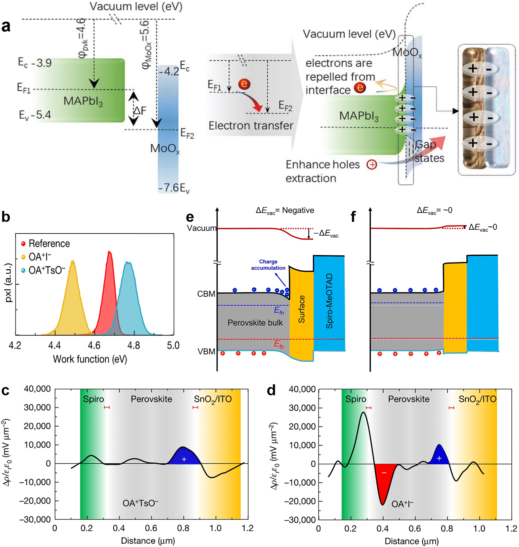 | ||
| Fig. 9 (a) Schematic diagram of additional interfacial dipole formed by inserting a MoOx interlayer. Reproduced from ref. 25 with permission from Wiley-VCH, copyright 2021. (b) Work function distributions measured by KPFM; Charge density distributions of (c) OATsO-treated and (d) OAI-treated device cross-sections measured by cross-sectional KPFM; schematic diagram of the heterointerface band alignments of the (e) OAI-treated and (f) OATsO-treated devices under illumination under open-circuit conditions. Reproduced from ref. 119 with permission from Springer Nature, copyright 2022. | ||
The success of applying MoOx with a high work function over the front surface of a perovskite in an n–i–p device motivated possible investigations on a similar consequence with other metal oxides. Besides vacuum deposition, atomic layer deposition (ALD) is a potential technology for the deposition of dielectric layers in order to achieve field-effect passivation in PSCs that require a mild preparation process. So far, the ALD technique has been used to deposit HTL/ETL (TiO2, SnO2, ZnO, and NiOx), recombination layers, and transparent conductive oxides for different device configurations. Ultrathin Al2O3 passivation layer (around 1 nm)121 could be fabricated by ALD for the chemical passivation of surface defects on perovskite film and successfully improved device efficiency and moisture stability.122 No corresponding characterization, however, has been performed to confirm its possible field-effect passivation, which deserves further investigation. Furthermore, other metal oxides with a high work function, such as VOx and WOx, also can form dielectric layers via ALD. To avoid the destructive effect of the water cycles of ALD,123 a p–i–n device structure is preferred and could be studied as the next step.
Very recently, Yang and his coworkers investigated the relationship between the work function change (ΔW) induced by surface treatment and the charge carrier dynamics at the interface.119 ΔW was described as the vacuum level change ΔEvac in this work. They applied OAI and OATsO to change the work function of the perovskite layers. According to the results of Kelvin probe force microscopy (KPFM), the work function of OAI-treated film decreased to 4.49 ± 0.09 V while that of the OATsO-treated film enhanced to 4.77 ± 0.11 V, from 4.67 ± 0.08 V of the reference (Fig. 9b), suggesting the negative ΔEvac of the OAI-treated film and non-negative ΔEvac of the OATsO-treated film. Charge carriers cannot be extracted under open-circuit conditions and may accumulate at the interface of the opposite polarity. Therefore, cross-sectional KPFM under illumination and open-circuit conditions was used to reveal the real-time charge carrier distribution in complete PSCs. As illustrated in Fig. 9c and d, moderate hole accumulation at the perovskite/ETL was observed for both OATsO-treated and OAI-treated PSCs, but a severe electron accumulation presented only at the perovskite/HTL interface for the OAI-treated PSC. These results demonstrate that non-negative ΔEvac enabled by interface passivators is conducive to avoiding the potential well and charge accumulation, consequently suppressing the possible halide migration, photocurrent hysteresis, and degradation of device performance (Fig. 10e and f). Besides the effective field-effect passivation, OA-based ammonium salts also provided chemical passivation effects. At nearly the same time, Zhu et al. achieved field-effect passivation of this type via benzylamine hydroiodide (BAHI) enabled chemical polishing.126 This treatment increased the work function and thus resulted in an up-shifted band structure near the polished perovskite surface, which produced an electric field facilitating the hole carrier collection. In conclusion, field-effect passivation achieved by promoting the work function of the perovskite layer to suppress this undesired interfacial behavior is an effective but easily overlooked passivation strategy.
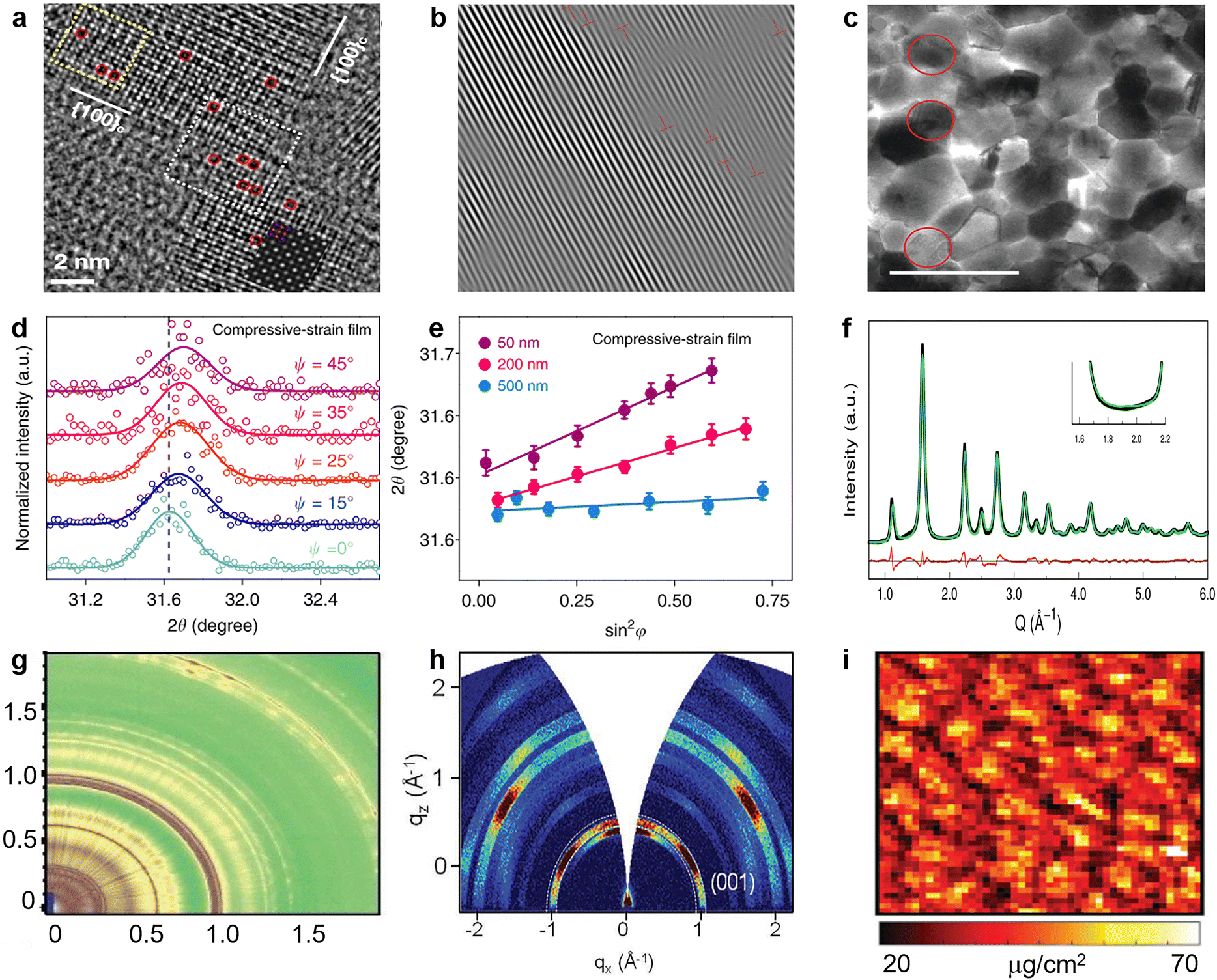 | ||
| Fig. 10 (a) Aberration-corrected high-resolution transmission electron microscopy (HRTEM) image of CsPbBr3 NCs (red dashed circles indicates Br vacancies). Reproduced from ref. 136 with permission from American Chemical Society, copyright 2021. (b) Inverse Fourier transform of the HRTEM image of the perovskite film. Reproduced from ref. 137 with permission from Elsevier, copyright 2020. (c) Bright-field TEM images recorded for the perovskite film with x = 0.5, the grains circled in red show {111}c planar defects. Reproduced from ref. 138 with permission from Springer Nature, copyright 2021. (d) GIXRD spectrum at different tilt angles at a depth of 50 nm for the compressively strained film; (e) residual strain distribution in the depths of 50, 200, and 500 nm for the compressively strained film. Reproduced from ref. 102 with permission from Springer Nature, copyright 2019. (f) Debye scattering equation best fit corresponding to orthorhombic coherent subdomains. Reproduced from ref. 147 with permission from American Chemical Society, copyright 2017. (g) 2D scattering patterns for TWAXS geometries. Reproduced from ref. 148 with permission from the Royal Society of Chemistry, copyright 2020. (h) Typical 2D GI-XRD pattern of the LHM-PVSK film. Reproduced from ref. 152 with permission from Wiley-VCH, copyright 2021. (i) Nano-XRF map of Cl illustrating the varying halide distribution within perovskite film over many grains. Reproduced from ref. 158 with permission from Wiley-VCH, copyright 2018. | ||
| Passivation type | Subcategory | Passivator/modification | Perovskite materials | PCE [%] | V OC [V] | J SC [mA cm−2] | FF (%) | Area [cm2] | Year/Ref. |
|---|---|---|---|---|---|---|---|---|---|
| a TPFP, tris(pentafluorophenyl)boron; b LAD, fluorine-containing hydrophobic Lewis acid; c TBPO, tribenzylphosphine oxide; d FDA, fluorination. 4,4′-(hexafluoroisopropylidene)diphthalic anhydride; e PVA, poly(vinyl acetate); f MBrA, methyl bromoacetate; g PEAI, phenethylammonium iodide; h EAI, ethylammonium iodide; i FPEAI, 2-(4-fluorophenyl)ethyl ammonium iodide; j DEA-DEDTC, diethylammonium diethyldithiocarbamate; k 4OH-NMI, 4-hydroxybiphenyl-substituted naphthalene-1,8-dicarboximide; l 9CN-PMI, cyanide-substituted perylene-3,4-dicarboximide; m Cl-SiNcTI, ambipolar silicon naphthalocyanine tetraimides; n NMAI, 1-naphthylmethylamine iodide; o TAPC, 4,4-cyclohexylidenebis[N,N-bis(4-methylphenyl)benzenamine]; p BAHI, benzylamine hydroiodide (BAHI). | |||||||||
| Chemical | Lewis acid | PCBB-3N-3I | MAPbI3 | 21.1 (17.7) | 1.11 (1.07) | 23.5 (22.61) | 81.4 (73.3) | 0.1 | 2019/127 |
| Chemical | Lewis acid | TPFPa | Cs0.05FA0.8MA0.15Pb(I0.83Br0.17)3 | 21.0 (18.0) | 1.16 (1.13) | 24.0 (22.6) | 71.0 76.0 | 0.04 | 2020/39 |
| Chemical | Lewis acid | LADb | CsFAMAPbIxBr1−x | 20.3 (13.4) | 1.12 (1.03) | 23.0 (21.0) | 79.0 (62.0) | — | 2020/40 |
| Chemical | Lewis base | Theophylline | (FAPbI3)x(MAPbBr3)1−x | 23.5 (21.0) | 1.19 (1.16) | 25.2 (24.8) | 78.0 (73.0) | — | 2019/42 |
| Chemical | Lewis base | TBPOc | CsFAMAPbIxBr1−x | 22.1 (20.4) | 1.14 (1.10) | 23.9 (23.7) | 81.0 (78.0) | — | 2020/54 |
| Chemical | Lewis base | FDAd | (FAPbI3)0.95(MAPbBr3)0.05 | 22.4 (19.6) | 1.16 (1.12) | 23.8 (22.5) | 81.5 (78.0) | 0.14 | 2021/128 |
| Chemical | Lewis base | PVAe | FAMAPbIxBr1−x | 23.2 (20.5) | 1.15 (1.12) | 25.2 (23.3) | 80.0 (78.5) | 0.1 | 2022/51 |
| Chemical | Lewis base | Indigo | Cs0.05FA0.85MA0.10Pb(I0.90Br0.10)3 | 23.2 (20.2) | 1.16 (1.07) | 25.0 (24.2) | 80.0 (78.0) | 0.0725 | 2022/53 |
| Chemical | Lewis base | MBrAf | FA0.85MA0.15PbI3 | 24.3 (22.3) | 1.18 (1.13) | 24.8 (24.6) | 82.9 (80.3) | 0.07 | 2022/129 |
| Chemical | Ammonium halide salts | PEAIg | FA1−xMAxPbI3 | 23.3 (21.5) | 1.18 (1.12) | 25.2 (24.3) | 78.4 (79.1) | 0.0739 | 2019/74 |
| Chemical | Ammonium halide salts | EAIh | FA0.9Cs0.07MA0.03Pb(I0.92Br0.08)3 | 22.4 (20.5) | 1.12 (1.08) | 24.1 (24.5) | 81.0 (76.0) | 0.16 | 2019/65 |
| Chemical | Ammonium halide salts | FPEAIi | Cs0.1(FA0.83MA0.17)0.9Pb(I0.83Br0.17)3 | 20.5 (19.2) | 1.13 (1.09) | 22.8 (22.0) | 80.0 (80.0) | 0.1 | 2019/76 |
| Chemical | Ammonium halide salts | DEA-DEDTCj | FAPbI3 | 23.2 (20.6) | 1.12 (1.08) | 25.8 (25.2) | 80.3 (76.0) | 0.1 | 2022/130 |
| Chemical | Metal cations | Ni2+ | MAPbI3 | 20.6 (17.3) | 1.13 (1.08) | 22.6 (21.6) | 81.0 74.0 | 0.108 | 2018/90 |
| Chemical | Metal cations | Eu3+ | MAPbI3 | 21.9 | 1.15 | 23.5 | 80.7 | 0.094 | 2019/80 |
| Chemical | Metal cations | Cd2+ | CsFAMAPbIxBr1−x | 22.0 (20.3) | 1.16 (1.14) | 24.9 (24.4) | 76.0 (73.0) | — | 2021/89 |
| Physical | Strain relaxation | — | FA0.85MA0.15Cs0.05Pb(I0.85Br0.15)3 | 20.7 | 1.17 | 22.8 | 78.0 | 2019/102 | |
| Physical | Thermal annealing treatment | — | CsFAMAPbIxBr1−x | 25.2 (21.4) | 1.23 (1.15) | 24.8 23.9 | 82.7 78.0 | 0.08313 | 2020/20 |
| Physical | Surface polishing | Femtosecond laser | Cs0.06FA0.79MA0.15Pb(I0.85Br0.15)3 | 18.6 (17.0) | 1.14 (1.08) | 23.3 (23.0) | 70.2 (68.5) | — | 2020/21 |
| Physical | Surface polishing | Adhesive tapes | Rb0.05Cs0.05FA0.85MA0.05PbI2.85Br0.15 | 22.0 (20.6) | 1.15 (1.12) | 23.4 (23.3) | 81.7 (78.8) | 0.08 | 2020/105 |
| Energetic | — | Perylene diimide | MAPbI3 | — | — | — | — | — | 2021/22 |
| Energetic | — | 4OH-NMIk | (FAPbI3)0.92(MAPbBr3)0.08 | 23.7 (21.1) | 1.15 (1.09) | 24.5 (24.2) | 83.9 (80.0) | 0.1 | 2021/23 |
| Energetic | — | 9CN-PMIl | (FAPbI3)0.92(MAPbBr3)0.08 | 21.5 (21.1) | 1.10 (1.09) | 24.2 (24.2) | 80.7 (80.0) | 0.1 | 2021/23 |
| Energetic | — | Cl-SiNcTIm | FA0.92MA0.08Pb(I0.92Br0.08)3 | 23.5 (21.7) | 1.18 (1.12) | 24.2 (23.8) | 82.4 (81.5) | 0.1 | 2022/116 |
| Field-effect | Organic molecules | NMAIn | Cs0.05(MA0.15FA0.85)0.95Pb(I0.85Br0.15)3 | 21.0 (19.4) | 1.18 (1.10) | 23.0 (22.7) | 77.3 77.3 | 0.1 | 2020/67 |
| Field-effect | Organic molecules | TAPCo | MAPbI3 | 21.5 (19.6) | 1.17 (1.15) | 22.9 (22.2) | 80.3 (76.9) | 0.1 | 2020/125 |
| Field-effect | Organic molecules | BAHIp | FA0.8075MA0.10Cs0.05Pb(I0.854Br0.186)3 | 24.5 (23.1) | 1.15 (1.12) | 25.9 (25.9) | 82.4 (79.5) | 0.09 | 2022/126 |
| Field-effect | Metal oxides | MoOx | MAPbI3 | 21.7 (19.1) | 1.18 (1.13) | 23.0 (21.9) | 80.1 (77.4) | 0.1 | 2021/25 |
| Field-effect | — | LiF | Cs0.05(MA0.17FA0.83)0.95Pb(I0.83Br0.17)3 | — | — | — | — | — | 2022/131 |
3. Characterization techniques of passivation strategies
3.1 Characterization for chemical and physical passivation
As strategies that directly reduce the defects of perovskite materials, chemical and physical passivation require advanced characterization techniques for identifying, observing, and quantifying the decrease of defects in perovskites or the consequently reduced non-radiative recombination, which therefore facilitate a better understanding of material properties, effects of defects, and device operations. Herein, we introduce various classical or novel advanced characterization techniques to reveal the passivation mechanisms under time- and/or space-resolved conditions. This section excludes the PL and space charge limited current (SCLC) characterization because they are well-known and widely reported in previous reviews. Notably, we selectively presented several synchrotron-based X-ray techniques and capacitance-based measurements by explaining the application cases on defect characterization and passivation in perovskites, which are gradually gaining attention in the field of PSCs.In the conventional p–n junction solar cell, the measured capacitance mainly comes from the charging and discharging of the defect at a location where the defect energy level crosses the Fermi level.171 The electron traps above or below the Fermi level are expected to be empty and filled, respectively. When the frequency of the alternating current (AC) voltage signal changes, the traps can release their charge within the AC period and therefore contribute to admittance. Another crucial factor affecting the release process of the charge is temperature because the traps with different activation energies induced by a temperature change can respond to the junction capacitance accordingly.
TAS measurement for PSCs in current research usually requires electrochemical potentiostat and temperature controlling equipment. The applied angular frequency ω defines an energetic demarcation:172
the trap density (NT) can be estimated from the angular frequency-dependent capacitance using
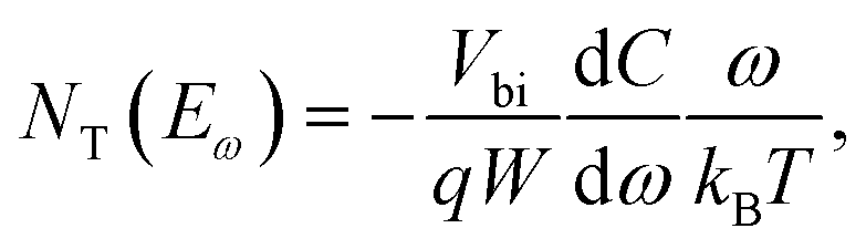
where C is the capacitance, k is the Boltzmann constant, Vbi is the built-in potential that depends on cutting off the edge of the curve from Mott–Schottky analysis, and W is the depletion width extracted from the slope of the fitting line of the same curve.10 The derived TAS plot is shown in Fig. 11a, which clearly differentiates the shallow-level and deep-level trap states and the drop of defect density after passivation.37 It should be noted that TAS has some shortcomings: it cannot distinguish the states between the valence band and conduction band, and the defect traps above the energy demarcation cannot be detected.
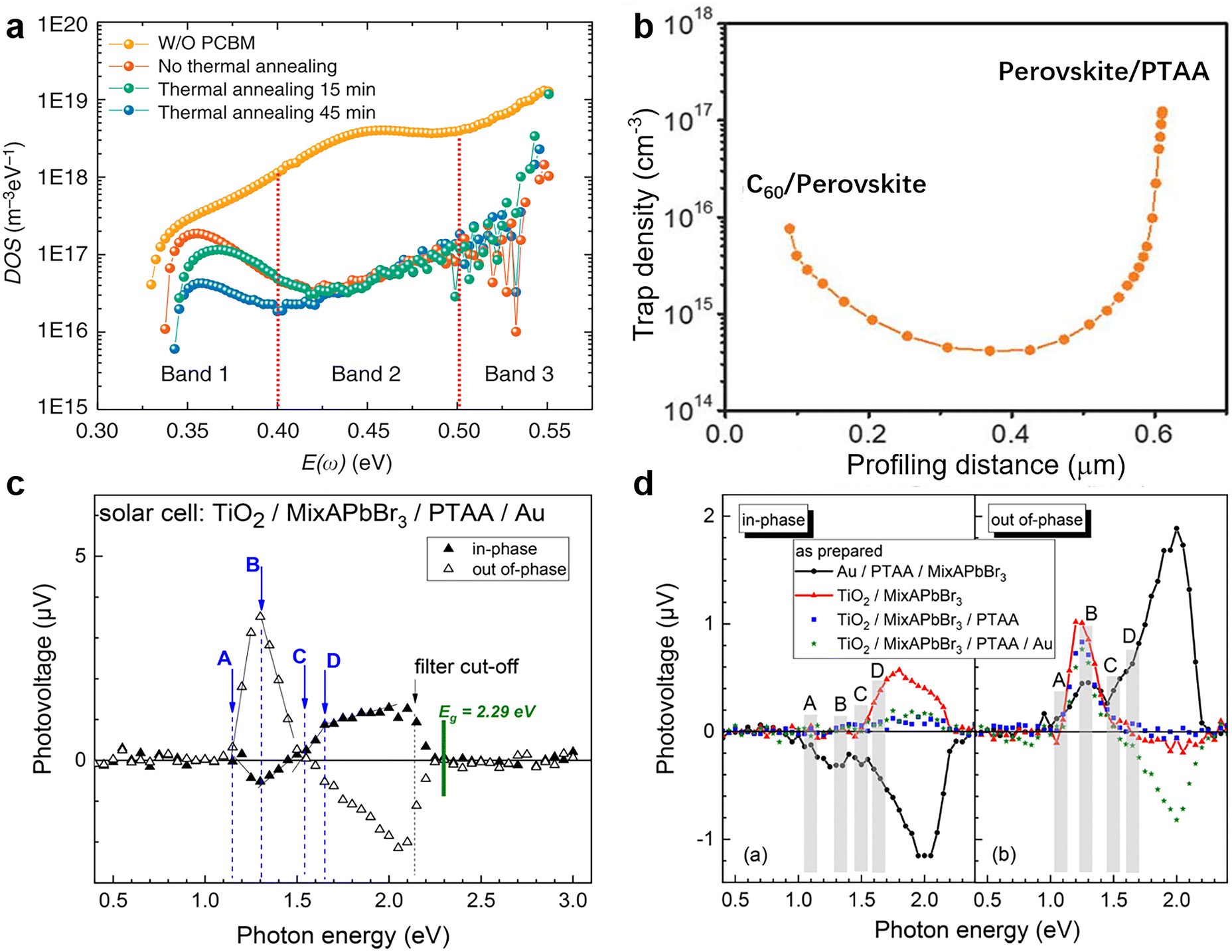 | ||
| Fig. 11 (a) Trap density of states obtained by TAS. Reproduced from ref. 37 with permission from Springer Nature, copyright 2014. (b) Dependence of the trap density on the profiling distance for the perovskite thin film by DLCP measurement. Reproduced from ref. 10 with permission from the AAAS, copyright 2020. (c) Spectra of the in-phase and out-of-phase SPV signals for the complete PSC structure; (d) spectra of the in-phase and out-of-phase SPV signals for different device structures. Reproduced from ref. 175 with permission from the American Chemical Society, copyright 2019. | ||
The derivation of the carrier density, including deep trap states, is based on the nonlinear relationship between the change of charges (δQ) and the perturbation AC bias (δV):
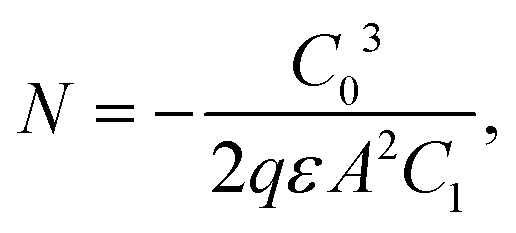
DLCP method uses a series of variables δV (e.g., 20 to 200 mV) to measure the junction capacitance and acquire the capacitance contribution from the trap states by taking advantage of the information embedded in the higher-order terms. For example, with the determination of C0 and C1, the carrier density (N) that includes both free carrier density (N0) and trap density (NT) at a particular position X from the junction barrier is calculated using:
In the modulated SPV spectroscopy, only the signals that can follow the charge separation and recovery of the light-induced disturbance of the space charge within the modulation period can be detected. In other words, the quasi-static charge distribution can change in a sample while measuring a modulated SPV spectrum. Through recording SPV responses under illumination, the resultant SPV spectroscopy can probe sub-band-gap electronic transitions caused by defect states and further determine the location of the corresponding defect states in terms of their energies within the bandgap.175–177 Thus, it can be used to confirm the passivation effect by chemical and physical passivation for the absorbing layer of PSCs. As shown in Fig. 11c and d, the modulated SPV spectrum combined in- and out-of-phase signals reveal several electronic transitions related to extrinsic (A) and intrinsic (B–D) defects at photon energies of about 0.9–1.15, 1.30–1.35, 1.50–1.55, and 1.65–1.70 eV, respectively. These four defect levels are over 0.6 eV from the band edges and therefore belong to the deep-level, and the corresponding defects serve as non-radiative recombination centers under steady-state illumination conditions.175
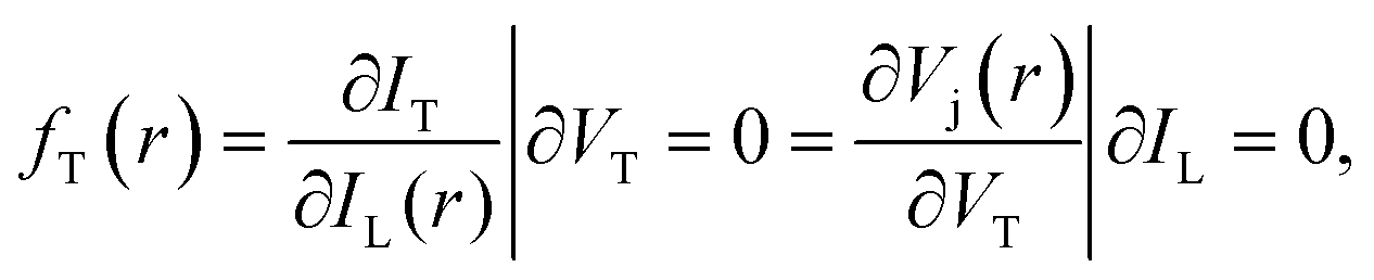
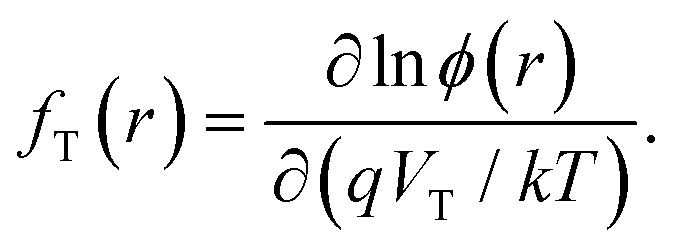
The samples measured by SRI are entire PSCs. The generalized Planck's law describes the radiative emission ϕ(E,r) of a solar cell:
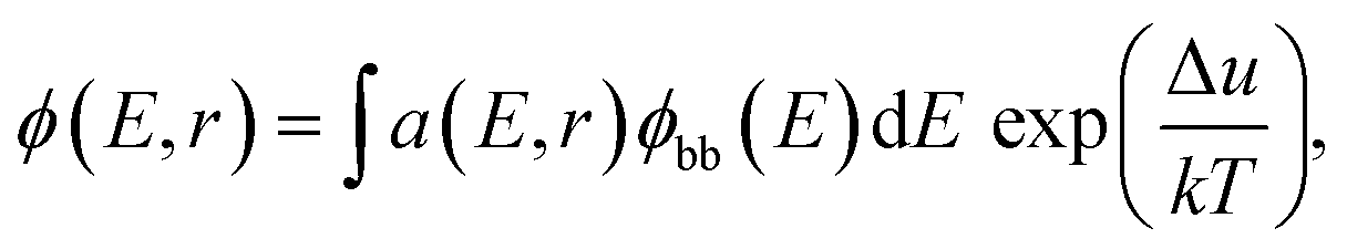
where IT is the terminal current of the cell, IL(r) is the local light-induced current, VT is the terminal voltage, Vj(r) is the local internal voltage when a terminal voltage of VT is applied. Based on above two equations, a luminescence-based reciprocity relation can be derived as follows:
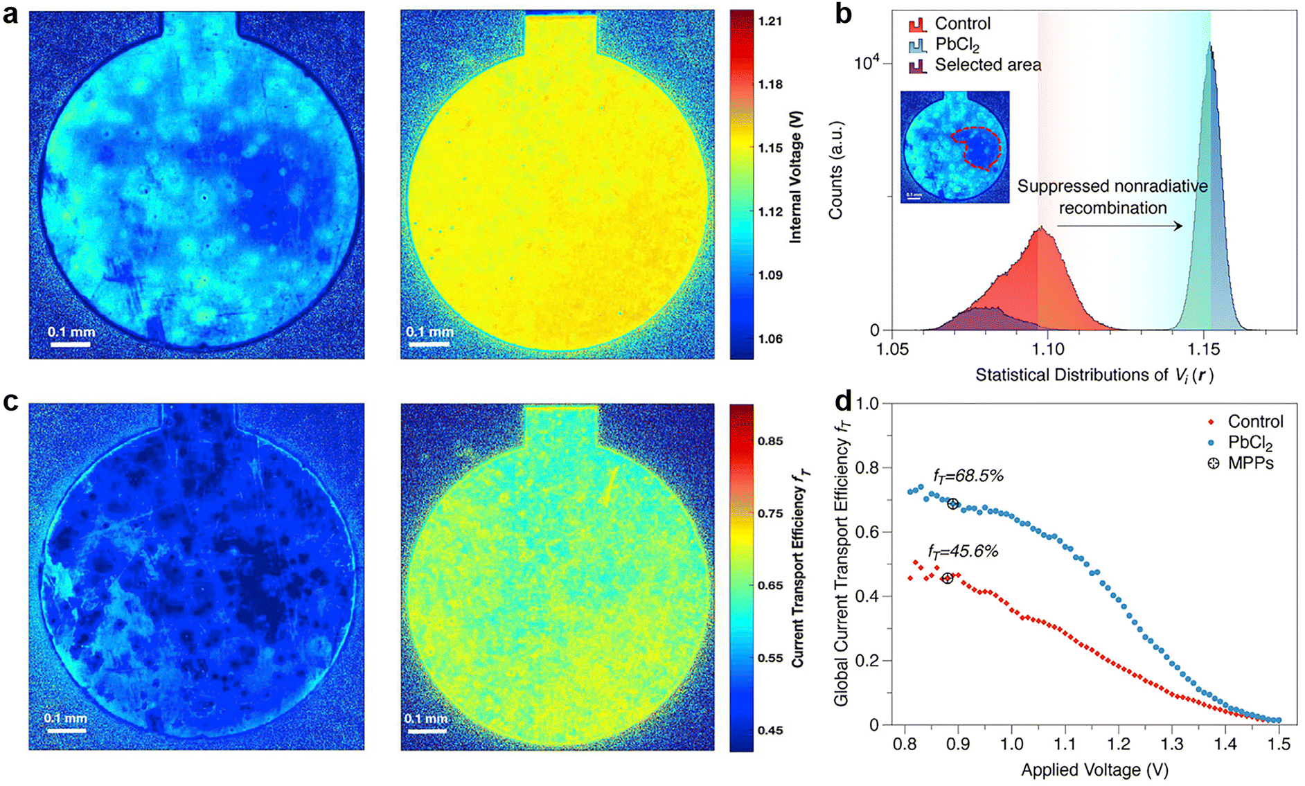 | ||
| Fig. 12 (a) Internal voltage map of the control and PbCl2-passivated devices; (b) statistical distributions of the local internal voltage counted from the Vi maps of these two devices; (c) current transport efficiency fT images of control and PbCl2-passivated devices; (d) globally averaged fT values of control and PbCl2-passivated devices as a function of the applied voltage. Reproduced from ref. 34 with permission from Elsevier, copyright 2020. | ||
The deducted fT images of reference and PbCl2-passivated PSCs are shown in Fig. 12c. For the reference sample, a large area of the device exhibits a high current transport loss. In contrast, the passivated sample displayed a noticeable enhancement in homogeneity of carrier transport and the corresponding fT values over the active area of the entire device.182Fig. 12d illustrates the globally averaged fT values of the corresponding PSCs as a function of the applied voltage determined via a series of luminescence images. Again, the PbCl2-passivated device shows a higher global fT at maximum power point than the control one, suggesting improved device-level current extraction capability.
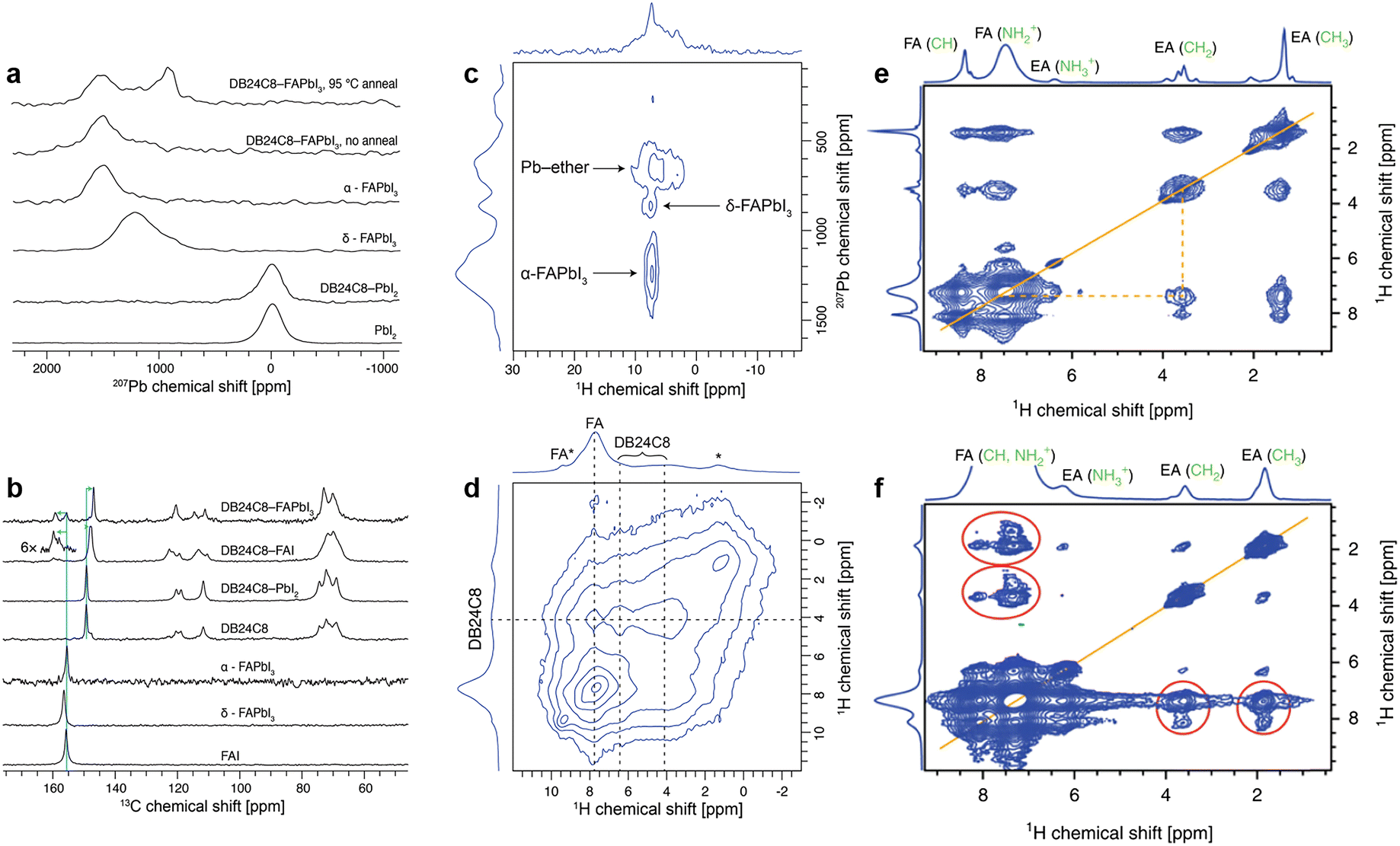
The chemical passivation effect of crown ether (DB24C8) for the uncoordinated Pb2+ defects and FA+ in FAPbI3 perovskite has been demonstrated via solid-state NMR spectroscopy.55 First, to confirm the possibility of complexation of FA+ and Pb2+ by DB24C8, bulk samples of FAI![[thin space (1/6-em)]](https://www.rsc.org/images/entities/char_2009.gif) :DB24C8 and PbI2:DB24C8 with a 1:1 molar ratio were recorded in ss-NMR. For DB24C8-PbI2, no change was observed either in the PbI2 structure as measured by the 207Pb spectrum (Fig. 13a) or in DB24C8 as probed by the 13C spectrum (Fig. 13b), which indicates that the crown ether is unable to form a complex with PbI2 under these conditions. While for DB24C8-FAI, an evident upfield shift of the 13C signal of the crown ether from 158.3 to 156.9 ppm indicates the change in the chemical environment of phenyl-ether (Fig. 13b). Combined with shifted 13C and 1H signals of FA+, the formation of a DB24C8-FAI complex was confirmed. Then the interaction between DB24C8 and bulk FAPbI3 perovskite was recorded. Although the a-FAPbI3 sample after ball-milling delivered an inconspicuous 207Pb signal around 1520 ppm, a new peak was observed at ∼900 ppm after annealing at 95 °C for 15 min, which may be ascribed to the signal from crown ether captured 207Pb (Fig. 13c). According to the distinguished signals of crown ether (1H, d = 4.2 ppm), perovskite FA+ (1H, d = 7.7 ppm), and aromatic ether (1H, d = 6.5 ppm) from Fig. 13d, the minor signal at d = 9.3 ppm can be assigned to FA+ interacting with the ether (denoted FA*). In brief, ss-NMR spectroscopy clearly verified the formation of a mixed perovskite-DB24C8 phase with atomic proximity between FA, Pb, and crown ether.55
:DB24C8 and PbI2:DB24C8 with a 1:1 molar ratio were recorded in ss-NMR. For DB24C8-PbI2, no change was observed either in the PbI2 structure as measured by the 207Pb spectrum (Fig. 13a) or in DB24C8 as probed by the 13C spectrum (Fig. 13b), which indicates that the crown ether is unable to form a complex with PbI2 under these conditions. While for DB24C8-FAI, an evident upfield shift of the 13C signal of the crown ether from 158.3 to 156.9 ppm indicates the change in the chemical environment of phenyl-ether (Fig. 13b). Combined with shifted 13C and 1H signals of FA+, the formation of a DB24C8-FAI complex was confirmed. Then the interaction between DB24C8 and bulk FAPbI3 perovskite was recorded. Although the a-FAPbI3 sample after ball-milling delivered an inconspicuous 207Pb signal around 1520 ppm, a new peak was observed at ∼900 ppm after annealing at 95 °C for 15 min, which may be ascribed to the signal from crown ether captured 207Pb (Fig. 13c). According to the distinguished signals of crown ether (1H, d = 4.2 ppm), perovskite FA+ (1H, d = 7.7 ppm), and aromatic ether (1H, d = 6.5 ppm) from Fig. 13d, the minor signal at d = 9.3 ppm can be assigned to FA+ interacting with the ether (denoted FA*). In brief, ss-NMR spectroscopy clearly verified the formation of a mixed perovskite-DB24C8 phase with atomic proximity between FA, Pb, and crown ether.55
 | ||
| Fig. 13 (a) 207Pb echo and (b) 1H → 13C CP NMR spectra of FAI, PbI2, and FAPbI3, with and without ball-milling with DB24C8 crown ether recorded at 15 kHz MAS. (c) 207Pb → 1H HETCOR spectrum of DB24C8-FAPbI3 recorded at 113 K and 30 kHz MAS. (d) 1H–1H spin diffusion spectrum of DB24C8-FAPbI3, recorded at 40 kHz MAS with a mixing time of 10 ms. Reproduced from ref. 55 with permission from the American Chemical Society, copyright 2020. (e) 1H–1H spin diffusion (20 kHz MAS) experiment evidencing atomic-level proximity between FA and EA in the mixed FA/EA phase; (f) 1H–1H spin diffusion experiment (60 kHz MAS) evidencing atomic-level proximity between FA and EA in FA0.93Cs0.07PbI3. Reproduced from ref. 65 with permission from Springer Nature, copyright 2019. | ||
In addition, ss-NMR spectroscopy could also be utilized to confirm the formation of a low-dimension passivation layer introduced by some ammonium halide salts.65 As illustrated in Fig. 13e, the magic angle spinning (MAS) ss-NMR of the ethyl ammonium iodide (EAI) treated CsFA perovskite film indicates completely converted EAI, judging from the new spectral signature similar to that of EAPbI3 (Fig. 13f). These results proved the existence of a fully converted 1D perovskite passivation layer without annealing in the new mixed EA/FA phases.65
3.2 Characterization for energetic passivation
The energetic passivator aims to create midgap states to capture photo-generated electrons before reacting with O2 to form superoxide, so its effectiveness is directly associated with the generation rate of superoxide species, which can be determined by the fluorescent molecular probe. Compounds with the ability to be fluorescent molecular probes, such as hydroethidine and 1,3-diphenylisobenzofuran (DPBF), are known to exhibit characteristic increase or decrease in emission at a specific wavelength upon exposure to the superoxide radical anion.24,109 The procedures for superoxide generation measurement are described as follows: (1) dissolving the fluorescent molecules in an organic solvent that cannot dissolve perovskite compositions (e.g. toluene) at specific proportions; (2) immersing the reference or passivated perovskite films into the above-mixed solution, and avoiding their contact with oxygen and light as much as possible; (3) building photodegradation conditions consisting of continuous illumination by a tungsten halogen lamp and dry oxygen flow bubbled through the organic solvent at a constant flow rate; (4) at regular time intervals, taking out a part of the mixed solutions after light/oxygen treatment as samples in a sealed container to avoid contact with oxygen and light; (5) transferring the above samples to cuvettes for recording the PL spectra at a specific excitation wavelength, where the corresponding fluorescence intensities at every time interval present the yield of the superoxide. As shown in Fig. 14a and b, the ratio IF(t)/IF(t0) is a measure of the yield of superoxide generation, where IF(t) is the fluorescence intensity maximum at time t and IF(t0) is the background fluorescence intensity of the probe at t = 0. The PL intensities vary with time, representing the increased rate of superoxide species in these perovskite films. The passivated samples deliver a lower rate of increase of superoxide species than the control one, implying the possible energetic passivation effect of the applied passivators.109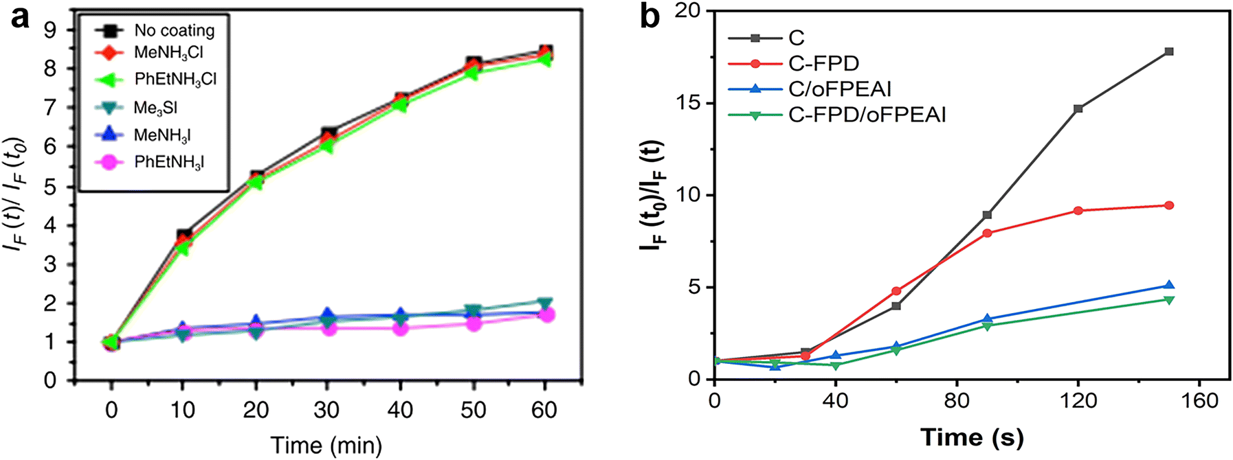 | ||
| Fig. 14 Superoxide generation plot for control perovskite and passivated perovskite films with (a) hydroethidine as the fluorescent probe. Reproduced from ref. 16 with permission from Springer Nature, copyright 2017. And (b) DPBF as a fluorescent probe. Reproduced from ref. 109 with permission from Wiley-VCH, copyright 2021. | ||
3.3 Characterization for field-effect passivation
The work function change or band bending at the interface of the perovskite layer and transporting layer is the crucial factor of field-effect passivation. Therefore, the field-effect passivation in PSCs can be confirmed by several energy-level-related characterization methods, including KPFM, XPS, and ultraviolet photoelectron spectroscopy (UPS) or their combination.The primary purpose of KPFM is to detect the surface potential change after inserting the dielectric layer. As illustrated in Fig. 15a, the sample to be tested should be divided into two regions, including the perovskite layer (Region 1) and the dielectric layer covered by the perovskite (Region 2).125 The KPFM results reveal large positive surface potential changes when the probe sweeps from the perovskite film to the perovskite-dielectric film (Fig. 15b). This phenomenon implies a microscopic electric dipole moment with the positive charge end pointing toward the perovskite film and the negative charge end pointing toward the dielectric layer, which is conducive to extracting holes and repelling electrons (Fig. 15c).117,192 It is also confirmed that the surface potential of the perovskite-dielectric film becomes more uniform than that of the perovskite film.125 Second, the contact potential difference (CPD) from KPFM can be used for determining the relative work function of the surface. CPD values between a metallic atomic force microscopy (AFM) tip and a sample and is denoted as VCPD, which is identified as the work function difference between the tip and the sample and can be expressed as follows:
| VCPD = Φtip − Φsimple/−e, |
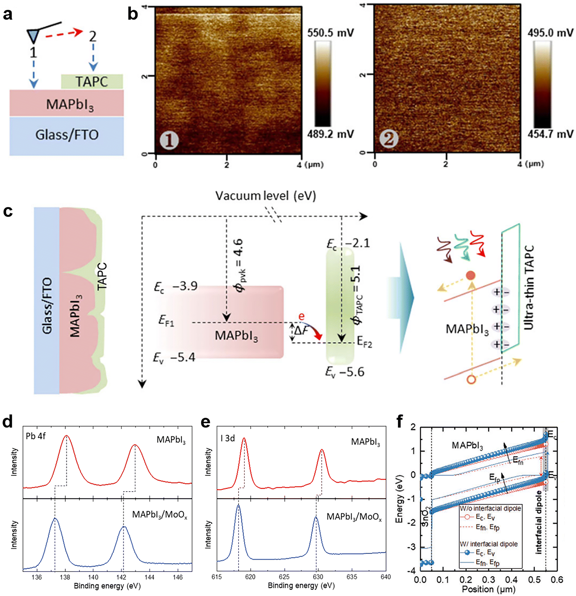 | ||
| Fig. 15 (a) The setup for SKPM measurement; (b) the SKPM images of the sample, region 1: the active layer (MAPbI3). Region 2: the TAPC covered MAPbI3; (c) schematic diagram of interface polarization formed by TAPC passivation. Reproduced from ref. 125 with permission from Springer Nature, copyright 2020. XPS spectra of (d) Pb 4f and (e) I 3d for MAPbI3 with and without MoOx; (f) the simulated energy band level with and without interfacial dipole. Reproduced from ref. 118 with permission from Wiley-VCH, copyright 2021. | ||
The XPS and UPS measurements also intend to investigate the work function and energy level alignment at the perovskite/passivation layer interface after field-effect passivation. Generally, the interface dipoles resulting from the selected dielectric layer will create band bending of the energy level at the perovskite surface close to the transporting layers, favorable for carrier collection due to better energy band alignment. As shown in Fig. 15d and e, after depositing MoOx as the dielectric layer, the lead and iodine core energy levels of the perovskite layer shift to the low binding energy position. These XPS results not only imply that the Ev (and core energy level) of the perovskite has moved to the Fermi level (EF) but also indicate that the bend of the bulk perovskite is bent upward to the rear surface, which is entirely due to the interface dipole caused by the high work function of the MoOx layer (Fig. 15f).25 As mentioned in Section 2.4, organic field-effect passivators are often accompanied by chemical passivation for charged defects due to the electronegativity of different parts of organic molecules or some specific functional groups. The dipoles created by interactions between organic field-effect passivators and the dominated negatively charged defects cause the upward bending of the energy level at the perovskite surface close to the HTL, promoting the hole collection due to better energy band alignment, which can be confirmed by UPS analysis.67,126
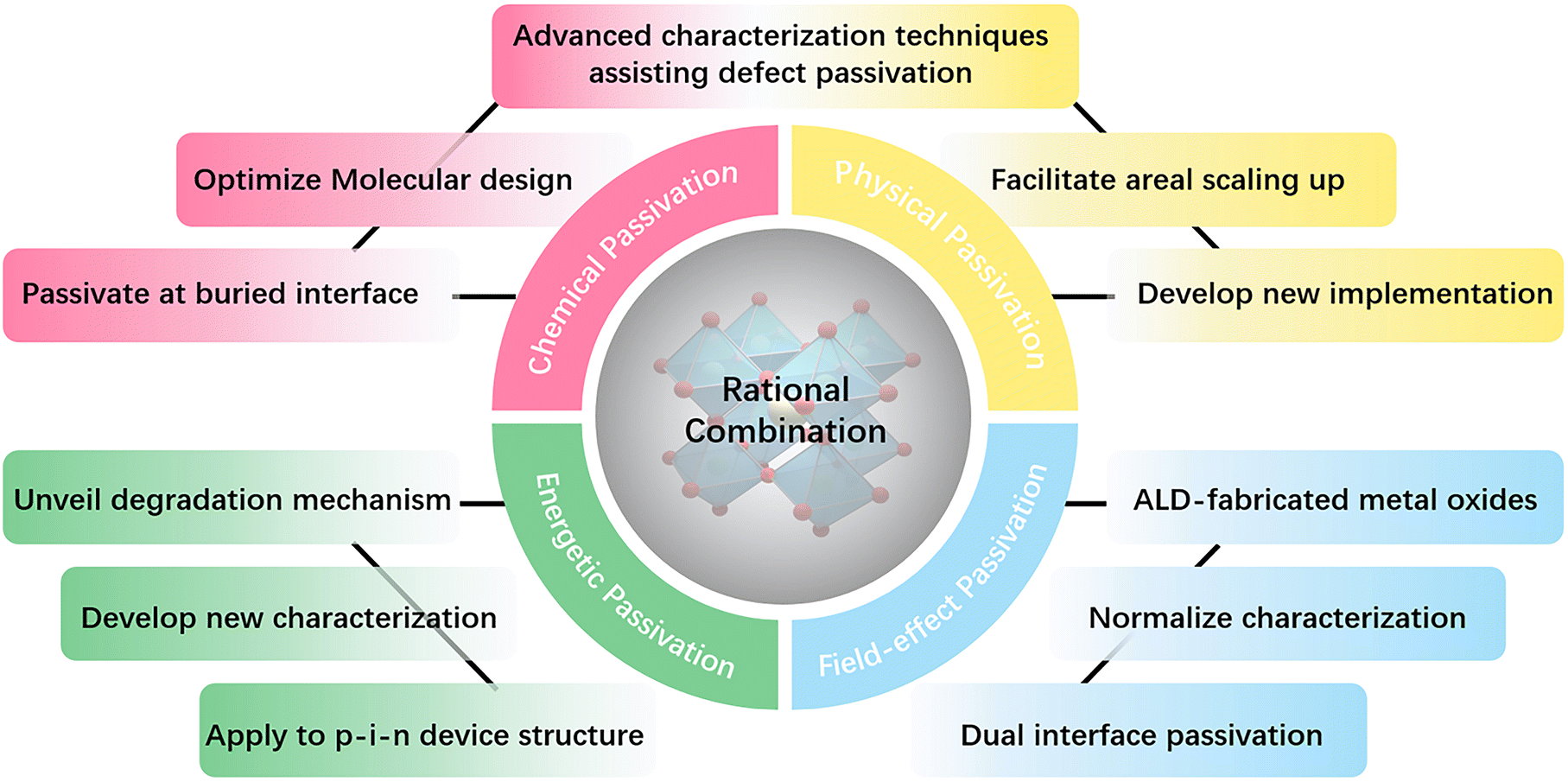 | ||
| Fig. 16 Summary of perspectives for chemical, physical, energetic, and field-effect passivation. | ||
The constant final state yield spectroscopy (CFSYS) was recently applied to investigate the electronic interface formation and energy level alignment between perovskite and ETL in inverted PCSs, in order to confirm field-effect passivation.131 This characterization is achieved by applying UPS with specific excitation energy and additionally varying the incident photon energy in the near-UV range and measuring the excited photoelectrons per absorbed photon (yield) at one constant final state (fixed kinetic energy). Through directly observing the Fermi edge in the CSFYS spectra, the measurement-induced surface photovoltage effects in the photoactive layer stacks and the energetic positions to the actual surface Fermi level can be accounted. By utilizing CFSYS, the field-effect passivation ability of the LiF interlayer at the perovskite/C60 interface was demonstrated, which resulted in a mild dipole effect and fixed charges that lowered the hole concentration in the vicinity of the interface.131
Overall, it should be pointed out that it is still challenging to accurately assess the underlying mechanisms of the four titled passivation strategies mentioned in this review based on the existing characterization techniques. Therefore, more advanced equipment and characterization are immediately needed to elucidate and demonstrate their working mechanisms from the experimental perspective in more depth. Potential examples include ultrafast spectroscopy to confirm the reduction process of Pb2+ by hot carriers, high-frequency electrical spectroscopy or highly sensitive chemical characterization equipment for in situ identification of superoxide anion, characterization of ultra-high spatial resolution to detect subtle passivation effect, and so on.
4. Conclusions and outlook
Albeit efficiency soared, the actual stability of the PSC devices still falls behind, which is regarded as the most significant impediment to their commercialization. Therefore, it is inevitable to utilize appropriate passivation strategies for fabricating PSCs with high photovoltaic performance and long-term stability. This review systematically outlined two prevailing passivation strategies (chemical and physical passivation) and two infrequently recognized passivation strategies (energetic and field-effect passivation), strengthening the fundamental understanding of their mechanism and cutting-edge characterization methods (Fig. 16).Chemical passivation mainly targets for the intrinsic point defects through chemical bonds and incidentally passivates three-dimensional and two-dimensional extended defects. Consequently, the VOC of passivated PSCs usually increases due to the suppressed defect-assisted non-radiative recombination resulting from the reduced deep-level defects. The suppressed migration and accumulation of shallow-level defects can subsequently mitigate the deleterious band bending, interfacial reactions, and phase segregation. According to the working mechanisms, Lewis acid/base compounds, ammonium halide salts, and some metal cationic passivating additives are classified as chemical passivators, which are universally used in high-efficiency photovoltaic devices. However, because of the intrinsically multifunctional nature of some chemical passivators (especially zwitterionic organic molecules), the overall complexity of the related research systems, as well as the limited experimental and characterization techniques, the complete mechanism of chemical passivation has not yet been totally resolved. Therefore, the rational and systematic molecular design principle of chemical passivators,54 including functional groups selection/combination,23,42 molecule stacking methods,41 the type and amount of halide anions,78,193etc., should be proposed or concluded to offer guidance to achieving highly-efficient chemical passivation.
It is worth mentioning that in perovskite films, the interface trap density (for both top and bottom surfaces) is several orders of magnitude higher than the bulk trap density.10 However, most passivation strategies used in reported studies only focus on the top surface of perovskite film and lack corresponding understanding and response for the non-exposed bottom surface, i.e., buried interface. In fact, the bottom surface of polycrystalline semiconductor films has more severe multi-scale heterogeneities and imperfections, limiting photovoltaic devices from reaching their performance potential to a great extent.194 Thus, designing new chemical passivation strategies to remove the non-radiative recombination-related defects at buried interfaces in perovskite photovoltaics and developing corresponding characterization methods also matter.195–197
The results of physical passivation generally resemble chemical passivation but with totally different mechanisms and implementations. This passivation method can be achieved by strain relaxation or physical treatments, including but not limited to introducing transition layers, post-treatment by cryo-temperature, and surface polishing. The superior effectiveness, universality, and accessibility of physical passivation enable the applicability in large-area PSC modules with low cost, which is hard to be achieved by chemical passivation. We note that more attention should be paid to future studies on physical passivation and practical implementation based on underlying mechanisms. Depending on the fabrication process of different components of the devices, combining chemical and physical passivation strategies to synergistically reduce absorber defects is an ingenious topic to be realized.
A thorough understanding of the nature, concentration, and distribution of different types of defects in perovskite films can also provide guidance for accurate chemical and physical passivation. Since the two key defect-related factors affecting the operational stability of perovskite devices are the trapped charges by deep-level defects and migration of shallow-level defects of perovskites, chemical and physical passivation targeted at reducing the defects of perovskite materials can significantly improve the device stability under operation. In order to pertinently enhance the operational stability of PSCs with different perovskite materials as absorbers, it is crucial to theoretically identify their main defect types that cause charge trapping or migration and apply the corresponding chemical or physical passivation strategies experimentally. In addition, a deeper understanding of the mechanism of moisture-, oxygen-, and light-induced degradation of PSCs under illumination is also fundamentally beneficial to identify the defect types. Several well-established or representative characterization methods are introduced to understand better the effect of chemical and physical passivation in reducing defects. For example, in order to identify defect types, quantize the defect state density, or confirm the degree of defect-assisted non-radiative recombination, synchrotron-based X-ray techniques, capacitance-based measurements, spatially resolved imaging techniques, etc., are discussed in detail.
As a recently proposed passivation strategy intended to improve light/oxygen stability, energetic passivation creates benign midgap states for the excited perovskite to capture the photoexcited electrons prior to oxygen and subsequently avoid the generation of superoxide anions. Consequently, the superoxide-induced perovskite degradation can be alleviated, preventing further damages caused by the resulting products such as H2O and I2, significantly improving the light and oxygen stability of PSCs. The protection effect will become more significant if the midgap state of energetic passivators (electron-accepting molecule) is closer to the CBM of perovskite due to fast electron trapping in the presence of strong NA coupling and a small energy gap.22,23 Aside from the generated midgap state by energetic passivators and the bandgap of the passivated system, more detailed design criteria need to be proposed for further studies. So far, most of the existing research about the effect of superoxide on perovskite has focused on MAPbI3. However, its potential role and detailed degradation mechanism in FA-containing perovskite or Cs-based inorganic perovskite are still vague.
On the other hand, Sn-based perovskites, as the less-toxic substitute for Pb-based perovskites, have attracted increasing attention because of their excellent optical bandgap and high charge-carrier mobility.198–200 Considering the extreme sensibility of the Sn-contained perovskite layer toward oxidation (Sn2+ to Sn4+) when exposed to oxidants, the superoxide anion radicals generated from the photo-excited electron can trigger the oxidation and serious decomposition of Sn-based perovskites,172 which deserves further investigation in the future study. Besides, the fluorescent molecular probe method for recording superoxide yields requires standard measurement protocols to ensure accuracy since the commonly used fluorescent molecular probe has limits under certain circumstances. Therefore, more effective and universal characterization strategies of energetic passivation need to be explored. In light of the mechanism and implementation of energetic passivation, it can also find application in PSCs with the p–i–n structure, where the demand for improving light/O2 stability is equally imperative.
Although many fabrication and characterization technologies of silicon solar cells have been successfully implemented in PSCs, field-effect passivation, as an efficient method that contributes to decreasing the probability of charge accumulation, reducing recombination velocity, and boosting charge transfer, is rarely reported in perovskite photovoltaics. Thus, this strategy can effectively suppress the performance degradation caused by charge migration and accumulation. The most critical factor in field-effect passivation is the selection of the dielectric layer, which determines the formation of interfacial dipoles and their working mechanisms. Metal oxides with high work function are ideal field-effect passivators with extra ability to prevent moisture penetration and provide stronger device stability due to the compactness and hydrophobicity of the dielectric layer they formed. On the other hand, organic molecules often have chemical passivation functionality due to the charged substituents, further improving device efficiency and stability (defect-related). Depending on the material properties, implementation methods of the dielectric layers vary accordingly, which are required to leave no or less damage to the perovskite layer. The unexplored ALD-fabricated metal oxides with similar dielectric behavior to Al2O3, such as Cr2O3, V2O5, and WO3, have great potential to be applied as a high-quality dielectric layer to achieve field-effect passivation. To avoid the possible degradation caused by water cycles in the growth process, deposition parameters such as employed precursors, water cycles, and temperature are required to be precisely optimized. Alternatively, other techniques without impairing perovskite layers should be developed for the deposition of the dielectric layer of metal oxides. To further promote the photovoltaic performance of PSCs, incorporating suitable dielectric layers at the opposite interface (ETL/perovskite or HTL/perovskite) should be considered, which may form bifacial field-effect passivation in PSCs to regulate recombination dynamics better.
Ultimately, considering the respective functions and the possible co-existence of chemical, physical, energetic, and field-effect passivation, we believe that the rational combinations among these passivation strategies can accelerate large-scale and practical manufacture of perovskite photovoltaics with excellent efficiency and stability.
Conflicts of interest
The authors declare no conflict of interest.Acknowledgements
P. G. acknowledges the National Natural Science Foundation of China (Grant No. 21975260, 22175180), the NSFC-CNR exchange program of NSFC (Grant No. 22011530391), and Fujian Science & Technology Innovation Laboratory for Optoelectronic Information of China (Grant No. 2021ZR113) for funding. R. L. is grateful to the National Natural Science Foundation of China (Grant No. 21973006) and the Beijing Natural Science Foundation (Grant No. 2212031).References
- Z. Zhang, Z. Li, L. Meng, S. Y. Lien and P. Gao, Adv. Funct. Mater., 2020, 30, 2001904 CrossRef CAS.
- C. Wang, Z. Song, C. Li, D. Zhao and Y. Yan, Adv. Funct. Mater., 2019, 29, 1808801 CrossRef CAS.
- X. Jiang, H. Li, Q. Zhou, Q. Wei, M. Wei, L. Jiang, Z. Wang, Z. Peng, F. Wang, Z. Zang, K. Xu, Y. Hou, S. Teale, W. Zhou, R. Si, X. Gao, E. H. Sargent and Z. Ning, J. Am. Chem. Soc., 2021, 143, 10970–10976 CrossRef CAS.
- J. Tong, Q. Jiang, A. J. Ferguson, A. F. Palmstrom, X. Wang, J. Hao, S. P. Dunfield, A. E. Louks, S. P. Harvey, C. Li, H. Lu, R. M. France, S. A. Johnson, F. Zhang, M. Yang, J. F. Geisz, M. D. Mcgehee, M. C. Beard, Y. Yan, D. Kuciauskas, J. J. Berry and K. Zhu, Nat. Energy, 2022, 7, 642–651 CrossRef CAS.
- L. Li, Y. Wang, X. Wang, R. Lin, X. Luo, Z. Liu, K. Zhou, S. Xiong, Q. Bao, G. Chen, Y. Tian, Y. Deng, K. Xiao, J. Wu, M. I. Saidaminov, H. Lin, C. Ma, Z. Zhao, Y. Wu, L. Zhang and H. Tan, Nat. Energy, 2022, 7, 708–717 CrossRef CAS.
- R. Lin, J. Xu, M. Wei, Y. Wang, Z. Qin, Z. Liu, J. Wu, K. Xiao, B. Chen, S. M. Park, G. Chen, H. R. Atapattu, K. R. Graham, J. Xu, J. Zhu, L. Li, C. Zhang, E. H. Sargent and H. Tan, Nature, 2022, 603, 73–78 CrossRef CAS.
- F. Zhang and K. Zhu, Adv. Energy Mater., 2020, 10, 1902579 CrossRef CAS.
- D. Li, D. Zhang, K. Lim, Y. Hu, Y. Rong, A. Mei, N. Park and H. Han, Adv. Funct. Mater., 2021, 31, 2008621 CrossRef CAS.
- S. P. Dunfield, L. Bliss, F. Zhang, J. M. Luther, K. Zhu, M. F. A. M. Van Hest, M. O. Reese and J. J. Berry, Adv. Energy Mater., 2020, 10, 1904054 CrossRef CAS.
- Z. Ni, C. Bao, Y. Liu, Q. Jiang, W. Q. Wu, S. Chen, X. Dai, B. Chen, B. Hartweg, Z. Yu, Z. Holman and J. Huang, Science, 2020, 367, 1352–1358 CrossRef CAS.
- B. Chen, P. N. Rudd, S. Yang, Y. Yuan and J. Huang, Chem. Soc. Rev., 2019, 48, 3842–3867 RSC.
- W.-J. Yin, T. Shi and Y. Yan, Appl. Phys. Lett., 2014, 104, 063903 CrossRef.
- R. Long, J. Liu and O. V. Prezhdo, J. Am. Chem. Soc., 2016, 138, 3884–3890 CrossRef CAS.
- X. Zheng, B. Chen, J. Dai, Y. Fang, Y. Bai, Y. Lin, H. Wei, X. C. Zeng and J. Huang, Nat. Energy, 2017, 2, 1–9 Search PubMed.
- Z. Li, C. Xiao, Y. Yang, S. P. Harvey, D. H. Kim, J. A. Christians, M. Yang, P. Schulz, S. U. Nanayakkara, C.-S. Jiang, J. M. Luther, J. J. Berry, M. C. Beard, M. M. Al-Jassim and K. Zhu, Energy Environ. Sci., 2017, 10, 1234–1242 RSC.
- N. Aristidou, C. Eames, I. Sanchez-Molina, X. Bu, J. Kosco, M. Saiful Islam and S. A. Haque, Nat. Commun., 2017, 8, 1–10 CrossRef PubMed.
- P. Zhao, B. J. Kim and H. S. Jung, Mater. Today Energy, 2018, 7, 267–286 CrossRef.
- H. Zhang, Y. Wu, C. Shen, E. Li, C. Yan, W. Zhang, H. Tian, L. Han and W. H. Zhu, Adv. Energy Mater., 2019, 9, 1803573 CrossRef.
- D. J. Xue, Y. Hou, S. C. Liu, M. Wei, B. Chen, Z. Huang, Z. Li, B. Sun, A. H. Proppe, Y. Dong, M. I. Saidaminov, S. O. Kelley, J. S. Hu and E. H. Sargent, Nat. Commun., 2020, 11, 1514 CrossRef CAS.
- Y. Chen, S. Tan, N. Li, B. Huang, X. Niu, L. Li, M. Sun, Y. Zhang, X. Zhang, C. Zhu, N. Yang, H. Zai, Y. Wu, S. Ma, Y. Bai, Q. Chen, F. Xiao, K. Sun and H. Zhou, Joule, 2020, 4, 1961–1976 CrossRef CAS.
- W. Kong, C. Zhao, J. Xing, Y. Zou, T. Huang, F. Li, J. Yang, W. Yu and C. Guo, Sol. RRL, 2020, 4, 2000189 CrossRef CAS.
- J. He, Y. Zhu, W. Fang and R. Long, J. Phys. Chem. Lett., 2021, 12, 1664–1670 CrossRef CAS PubMed.
- Z. Zhang, Y. Gao, Z. Li, L. Qiao, Q. Xiong, L. Deng, Z. Zhang, R. Long, Q. Zhou, Y. Du, Z. Lan, Y. Zhao, C. Li, K. Müllen and P. Gao, Adv. Mater., 2021, 33, 2008405 CrossRef CAS PubMed.
- N. Aristidou, I. Sanchez-Molina, T. Chotchuangchutchaval, M. Brown, L. Martinez, T. Rath and S. A. Haque, Angew. Chem., 2015, 127, 8326–8330 CrossRef.
- F. Wang, Y. Zhang, M. Yang, D. Han, L. Yang, L. Fan, Y. Sui, Y. Sun, X. Liu, X. Meng and J. Yang, Adv. Funct. Mater., 2021, 31, 2008052 CrossRef CAS.
- J. Kim, A. Ho-Baillie and S. Huang, Sol. RRL, 2019, 3, 1800302 CrossRef.
- S. Akin, N. Arora, S. M. Zakeeruddin, M. Grätzel, R. H. Friend and M. I. Dar, Adv. Energy Mater., 2020, 10, 1903090 CrossRef CAS.
- A. Abate, M. Saliba, D. J. Hollman, S. D. Stranks, K. Wojciechowski, R. Avolio, G. Grancini, A. Petrozza and H. J. Snaith, Nano Lett., 2014, 14, 3247–3254 CrossRef CAS PubMed.
- P. Metrangolo, L. Canil, A. Abate, G. Terraneo and G. Cavallo, Angew. Chem., Int. Ed., 2022, 61, e202114793 CrossRef CAS PubMed.
- M. A. Ruiz-Preciado, D. J. Kubicki, A. Hofstetter, L. McGovern, M. H. Futscher, A. Ummadisingu, R. Gershoni-Poranne, S. M. Zakeeruddin, B. Ehrler, L. Emsley, J. V. Milić and M. Grätzel, J. Am. Chem. Soc., 2020, 142, 1645–1654 CrossRef CAS PubMed.
- C. Ma and N. G. Park, ACS Energy Lett., 2020, 5, 3268–3275 CrossRef CAS.
- M. J. Choi, Y. S. Lee, I. H. Cho, S. S. Kim, D. H. Kim, S. N. Kwon and S. I. Na, Nano Energy, 2020, 71, 104639 CrossRef CAS.
- J. J. Yoo, G. Seo, M. R. Chua, T. G. Park, Y. Lu, F. Rotermund, Y. K. Kim, C. S. Moon, N. J. Jeon, J. P. Correa-Baena, V. Bulović, S. S. Shin, M. G. Bawendi and J. Seo, Nature, 2021, 590, 587–593 CrossRef CAS PubMed.
- A. Ren, H. Lai, X. Hao, Z. Tang, H. Xu, B. M. F. Yu Jeco, K. Watanabe, L. Wu, J. Zhang, M. Sugiyama, J. Wu and D. Zhao, Joule, 2020, 4, 1263–1277 CrossRef CAS.
- H. Zhang, M. K. Nazeeruddin and W. C. H. Choy, Adv. Mater., 2019, 31, 1805702 CrossRef.
- R. C. Haddon, New Ser., 1993, 261, 1545–1550 CAS.
- Y. Shao, Z. Xiao, C. Bi, Y. Yuan and J. Huang, Nat. Commun., 2014, 5, 5784 CrossRef CAS PubMed.
- J. Xu, A. Buin, A. H. Ip, W. Li, O. Voznyy, R. Comin, M. Yuan, S. Jeon, Z. Ning, J. J. McDowell, P. Kanjanaboos, J. P. Sun, X. Lan, L. N. Quan, D. H. Kim, I. G. Hill, P. Maksymovych and E. H. Sargent, Nat. Commun., 2015, 6, 7081 CrossRef CAS.
- Z. Yang, J. Dou, S. Kou, J. Dang, Y. Ji, G. Yang, W. Q. Wu, D. Bin Kuang and M. Wang, Adv. Funct. Mater., 2020, 30, 1910710 CrossRef CAS.
- J. Luo, J. Xia, H. Yang, H. A. Malik, F. Han, H. Shu, X. Yao, Z. Wan and C. Jia, Nano Energy, 2020, 70, 104509 CrossRef CAS.
- Y. Lin, L. Shen, J. Dai, Y. Deng, Y. Wu, Y. Bai, X. Zheng, J. Wang, Y. Fang, H. Wei, W. Ma, X. C. Zeng, X. Zhan and J. Huang, Adv. Mater., 2017, 29, 1604545 CrossRef.
- R. Wang, J. Xue, K.-L. Wang, Z.-K. Wang, Y. Luo, D. Fenning, G. Xu, S. Nuryyeva, T. Huang, Y. Zhao, J. L. Yang, J. Zhu, M. Wang, S. Tan, I. Yavuz, K. N. Houk and Y. Yang, Science, 2019, 366, 1509–1513 CrossRef CAS.
- N. K. Noel, A. Abate, S. D. Stranks, E. S. Parrott, V. M. Burlakov, A. Goriely and H. J. Snaith, ACS Nano, 2014, 8, 9815–9821 CrossRef CAS.
- J. He, W. H. Fang, R. Long and O. V. Prezhdo, Nano Energy, 2021, 79, 105491 CrossRef CAS.
- L. Liu, W. H. Fang, R. Long and O. V. Prezhdo, J. Phys. Chem. Lett., 2018, 9, 1164–1171 CrossRef CAS PubMed.
- C. Mai, Q. Zhou, Q. Xiong, C. Chen, J. Xu, Z. Zhang, H. Lee, C. Yeh and P. Gao, Adv. Funct. Mater., 2021, 31, 2007762 CrossRef CAS.
- L. Qiao, W. H. Fang, R. Long and O. V. Prezhdo, J. Am. Chem. Soc., 2021, 143, 9982–9990 CrossRef CAS PubMed.
- J.-W. Lee, S.-H. Bae, Y.-T. Hsieh, N. De Marco, M. Wang, P. Sun and Y. Yang, Chem, 2017, 3, 290–302 CAS.
- L. Deng, Z. Zhang, Y. Gao, Q. Xiong, Z. Li, J. Xu, Z. Zhang, J. Chen and P. Gao, Sustainable Energy Fuels, 2021, 5, 2347–2353 RSC.
- L. Liang, Q. Xiong, Z. Zhang, Y. Yu and P. Gao, Electrochim. Acta, 2022, 413, 140172 CrossRef CAS.
- M. Wang, Y. Zhao, X. Jiang, S. Jin, M. Wang, Y. Zhao, X. Jiang, Y. Yin, I. Yavuz and P. Zhu, Joule, 2022, 6, 1032–1048 CrossRef CAS.
- F. Zhang, D. Bi, N. Pellet, C. Xiao, Z. Li, J. J. Berry, S. M. Zakeeruddin, K. Zhu and M. Grätzel, Energy Environ. Sci., 2018, 11, 3480–3490 RSC.
- J. Guo, J. Sun, L. Hu, S. Fang, X. Ling, X. Zhang, Y. Wang, H. Huang, C. Han, C. Cazorla, Y. Yang, D. Chu, T. Wu, J. Yuan and W. Ma, Adv. Energy Mater., 2022, 12, 2200537 CrossRef CAS.
- H. Li, J. Shi, J. Deng, Z. Chen, Y. Li, W. Zhao, J. Wu, H. Wu, Y. Luo, D. Li and Q. Meng, Adv. Mater., 2020, 32, 1907396 CrossRef CAS.
- T. Sen, Su, F. T. Eickemeyer, M. A. Hope, F. Jahanbakhshi, M. Mladenović, J. Li, Z. Zhou, A. Mishra, J. H. Yum, D. Ren, A. Krishna, O. Ouellette, T. C. Wei, H. Zhou, H. H. Huang, M. D. Mensi, K. Sivula, S. M. Zakeeruddin, J. V. Milić, A. Hagfeldt, U. Rothlisberger, L. Emsley, H. Zhang and M. Grätzel, J. Am. Chem. Soc., 2020, 142, 19980–19991 CrossRef.
- H. Zhang, F. T. Eickemeyer, Z. Zhou, M. Mladenović, F. Jahanbakhshi, L. Merten, A. Hinderhofer, M. A. Hope, O. Ouellette, A. Mishra, P. Ahlawat, D. Ren, T. Sen Su, A. Krishna, Z. Wang, Z. Dong, J. Guo, S. M. Zakeeruddin, F. Schreiber, A. Hagfeldt, L. Emsley, U. Rothlisberger, J. V. Milić and M. Grätzel, Nat. Commun., 2021, 12, 3383 CrossRef CAS.
- F. Zhang, S. Y. Park, C. Yao, H. Lu, S. P. Dunfield, C. Xiao, S. Uličná, X. Zhao, L. D. Hill, X. Chen, X. Wang, L. E. Mundt, K. H. Stone, L. T. Schelhas, G. Teeter, S. Parkin, E. L. Ratcliff, Y. Loo, J. J. Berry, M. C. Beard, Y. Yan, B. W. Larson and K. Zhu, Science, 2021, 375, 71–76 CrossRef PubMed.
- F. Zhang, H. Lu, J. Tong, J. J. Berry, M. C. Beard and K. Zhu, Energy Environ. Sci., 2020, 13, 1154–1186 RSC.
- D. L. Mcgott, C. P. Muzzillo, C. L. Perkins, J. J. Berry, K. Zhu, J. N. Duenow, E. Colegrove, C. A. Wolden and M. O. Reese, Joule, 2021, 5, 1057–1073 CrossRef CAS.
- Y. Gao, Z. Wei, S. N. Hsu, B. W. Boudouris and L. Dou, Mater. Chem. Front., 2020, 4, 3400–3418 RSC.
- J. V. Milić, J. Mater. Chem. C, 2021, 9, 11428–11443 RSC.
- F. Gao, Y. Zhao, X. Zhang and J. You, Adv. Energy Mater., 2020, 10, 1902650 CrossRef CAS.
- P. Gao, A. R. Bin Mohd Yusoff and M. K. Nazeeruddin, Nat. Commun., 2018, 9, 5028 CrossRef.
- M. M. Tavakoli, W. Tress, J. V. Milić, D. Kubicki, L. Emsley and M. Grätzel, Energy Environ. Sci., 2018, 11, 3310–3320 RSC.
- E. A. Alharbi, A. Y. Alyamani, D. J. Kubicki, A. R. Uhl, B. J. Walder, A. Q. Alanazi, J. Luo, A. Burgos-Caminal, A. Albadri, H. Albrithen, M. H. Alotaibi, J. E. Moser, S. M. Zakeeruddin, F. Giordano, L. Emsley and M. Grätzel, Nat. Commun., 2019, 10, 3008 CrossRef.
- Z. Wang, Q. Lin, F. P. Chmiel, N. Sakai, L. M. Herz and H. J. Snaith, Nat. Energy, 2017, 2, 1–10 Search PubMed.
- L. Liang, H. Luo, J. Hu, H. Li and P. Gao, Adv. Energy Mater., 2020, 10, 2000197 CrossRef CAS.
- Y. Hu, J. Schlipf, M. Wussler, M. L. Petrus, W. Jaegermann, T. Bein, P. Müller-Buschbaum and P. Docampo, ACS Nano, 2016, 10, 5999–6007 CrossRef CAS PubMed.
- M. Jung, T. J. Shin, J. Seo, G. Kim and S. Il Seok, Energy Environ. Sci., 2018, 11, 2188–2197 RSC.
- J. J. Yoo, S. Wieghold, M. C. Sponseller, M. R. Chua, S. N. Bertram, N. T. P. Hartono, J. S. Tresback, E. C. Hansen, J.-P. Correa-Baena, V. Bulović, T. Buonassisi, S. S. Shin and M. G. Bawendi, Energy Environ. Sci., 2019, 12, 2192–2199 RSC.
- Y. Zhang, Z. Fei, P. Gao, Y. Lee, F. F. Tirani, R. Scopelliti, Y. Feng, P. J. Dyson and M. K. Nazeeruddin, Adv. Mater., 2017, 29, 1702157 CrossRef.
- S. Yang, J. Dai, Z. Yu, Y. Shao, Y. Zhou, X. Xiao, X. C. Zeng and J. Huang, J. Am. Chem. Soc., 2019, 141, 5781–5787 CrossRef CAS PubMed.
- L. Qiao, W. H. Fang and R. Long, J. Phys. Chem. Lett., 2022, 13, 954–961 CrossRef CAS PubMed.
- Q. Jiang, Y. Zhao, X. Zhang, X. Yang, Y. Chen, Z. Chu, Q. Ye, X. Li, Z. Yin and J. You, Nat. Photonics, 2019, 13, 460–466 CrossRef CAS.
- N. Li, S. Tao, Y. Chen, X. Niu, C. K. Onwudinanti, C. Hu, Z. Qiu, Z. Xu, G. Zheng, L. Wang, Y. Zhang, L. Li, H. Liu, Y. Lun, J. Hong, X. Wang, Y. Liu, H. Xie, Y. Gao, Y. Bai, S. Yang, G. Brocks, Q. Chen and H. Zhou, Nat. Energy, 2019, 4, 408–415 CrossRef CAS.
- Q. Zhou, L. Liang, J. Hu, B. Cao, L. Yang, T. Wu, X. Li, B. Zhang and P. Gao, Adv. Energy Mater., 2019, 9, 1–11 Search PubMed.
- Q. Zhou, Q. Xiong, Z. Zhang, J. Hu, F. Lin, L. Liang, T. Wu, X. Wang, J. Wu, B. Zhang and P. Gao, Sol. RRL, 2020, 4, 2000107 CrossRef CAS.
- L. Wang, Q. Zhou, Z. Zhang, W. Li, X. Wang, Q. Tian, X. Yu, T. Sun, J. Wu, B. Zhang and P. Gao, J. Energy Chem., 2022, 64, 179–189 CrossRef CAS.
- H. Shen, T. Duong, J. Peng, D. Jacobs, N. Wu, J. Gong, Y. Wu, S. K. Karuturi, X. Fu, K. Weber, X. Xiao, T. P. White and K. Catchpole, Energy Environ. Sci., 2018, 11, 394–406 RSC.
- L. Wang, H. Zhou, J. Hu, B. Huang, M. Sun, B. Dong, G. Zheng, Y. Huang, Y. Chen, L. Li, Z. Xu, N. Li, Z. Liu, Q. Chen, L. D. Sun and C. H. Yan, Science, 2019, 363, 265–270 CrossRef CAS.
- C. Bi, X. Zheng, B. Chen, H. Wei and J. Huang, ACS Energy Lett., 2017, 2, 1400–1406 CrossRef CAS.
- M. Abdi-Jalebi, Z. Andaji-Garmaroudi, S. Cacovich, C. Stavrakas, B. Philippe, J. M. Richter, M. Alsari, E. P. Booker, E. M. Hutter, A. J. Pearson, S. Lilliu, T. J. Savenije, H. Rensmo, G. Divitini, C. Ducati, R. H. Friend and S. D. Stranks, Nature, 2018, 555, 497–501 CrossRef CAS PubMed.
- D.-Y. Son, S.-G. Kim, J.-Y. Seo, S.-H. Lee, H. Shin, D. Lee and N.-G. Park, J. Am. Chem. Soc., 2018, 140, 1358–1364 CrossRef CAS PubMed.
- F. Zheng, W. Chen, T. Bu, K. P. Ghiggino, F. Huang, Y. Cheng, P. Tapping, T. W. Kee, B. Jia and X. Wen, Adv. Energy Mater., 2019, 9, 1–11 Search PubMed.
- M. Abdi-jalebi, M. Pazoki, B. Philippe, M. I. Dar, M. Alsari, A. Sadhanala, R. Imani, S. Lilliu, J. Kullgren, H. Rensmo, M. Grätzel and R. H. Friend, ACS Nano, 2018, 12, 7301–7311 CrossRef CAS PubMed.
- X. Shai, L. Zuo, P. Sun, P. Liao, W. Huang, E. Yao, H. Li, S. Liu, Y. Shen, Y. Yang and M. Wang, Nano Energy, 2017, 36, 213–222 CrossRef CAS.
- W. S. Subhani, K. Wang, M. Du and S. F. Liu, Nano Energy, 2019, 61, 165–172 CrossRef CAS.
- W. Xiang, Z. Wang, D. J. Kubicki, M. Gra, W. Xiang, Z. Wang, D. J. Kubicki, W. Tress, J. Luo, D. Prochowicz, S. Akin, L. Emsley, J. Zhou and G. Dietler, Joule, 2019, 3, 205–214 CrossRef CAS.
- M. Ji, M. Jin, Q. Du, J. Zheng, Y. Feng, Z. Shen, F. Li, H. Li and C. Chen, ACS Appl. Energy Mater., 2021, 4, 11144–11150 CrossRef CAS.
- X. Gong, L. Guan, H. Pan, Q. Sun, X. Zhao, H. Li, H. Pan, Y. Shen, Y. Shao, L. Sun, Z. Cui, L. Ding and M. Wang, Adv. Funct. Mater., 2018, 28, 1804286 CrossRef.
- E. Mosconi, A. Amat, M. K. Nazeeruddin, M. Grätzel and F. De Angelis, J. Phys. Chem. C, 2013, 117, 13902–13913 CrossRef CAS.
- M. I. Dar, G. Jacopin, S. Meloni, A. Mattoni, N. Arora, A. Boziki, S. M. Zakeeruddin, U. Rothlisberger and M. Grätzel, Sci. Adv., 2016, 2, e1601156 CrossRef.
- M. Abdi-Jalebi, Z. Andaji-Garmaroudi, A. J. Pearson, G. Divitini, S. Cacovich, B. Philippe, H. Rensmo, C. Ducati, R. H. Friend and S. D. Stranks, ACS Energy Lett., 2018, 3, 2671–2678 CrossRef CAS PubMed.
- L. Qiao, W. Fang, R. Long and O. V. Prezhdo, Angew. Chem., Int. Ed., 2020, 59, 4684–4690 CrossRef CAS PubMed.
- C. C. Zhang, S. Yuan, Y. H. Lou, H. Okada and Z. K. Wang, Small, 2022, 2107556 CrossRef CAS.
- J. T.-W. Wang, Z. Wang, S. Pathak, W. Zhang, D. W. DeQuilettes, F. Wisnivesky-Rocca-Rivarola, J. Huang, P. K. Nayak, J. B. Patel, H. A. Mohd Yusof, Y. Vaynzof, R. Zhu, I. Ramirez, J. Zhang, C. Ducati, C. Grovenor, M. B. Johnston, D. S. Ginger, R. J. Nicholas and H. J. Snaith, Energy Environ. Sci., 2016, 9, 2892–2901 RSC.
- X. Zheng, C. Wu, S. K. Jha, Z. Li, K. Zhu and S. Priya, ACS Energy Lett., 2016, 1, 1014–1020 CrossRef CAS.
- M. Faghihnasiri, M. Izadifard and M. E. Ghazi, Phys. B, 2020, 582, 412024 CrossRef CAS.
- Y. Jiao, S. Yi, H. Wang, B. Li, W. Hao, L. Pan, Y. Shi, X. Li, P. Liu, H. Zhang, C. Gao, J. Zhao and J. Lu, Adv. Funct. Mater., 2021, 31, 2006243 CrossRef CAS.
- K. M. Boopathi, B. Martín-García, A. Ray, J. M. Pina, S. Marras, M. I. Saidaminov, F. Bonaccorso, F. Di Stasio, E. H. Sargent, L. Manna and A. L. Abdelhady, ACS Energy Lett., 2021, 5, 642–649 CrossRef.
- L. Kong, G. Liua, J. Gong, Q. Hu, R. D. Schaller, P. Dera, D. Zhang, Z. Liu, W. Yang, K. Zhu, Y. Tang, C. Wang, S. H. Wei, T. Xu and H. K. Mao, Proc. Natl. Acad. Sci. U. S. A., 2016, 113, 8910–8915 CrossRef CAS.
- C. Zhu, X. Niu, Y. Fu, N. Li, C. Hu, Y. Chen, X. He, G. Na, P. Liu, H. Zai, Y. Ge, Y. Lu, X. Ke, Y. Bai, S. Yang, P. Chen, Y. Li, M. Sui, L. Zhang, H. Zhou and Q. Chen, Nat. Commun., 2019, 10, 815 CrossRef CAS.
- Z. Z. Faming Li, W. Zhu, C. Bao, T. Yu, Y. Wang and X. Zhou, Chem. Commun., 2016, 52, 5394–5397 RSC.
- P. You, G. Li, G. Tang, J. Cao and F. Yan, Energy Environ. Sci., 2020, 13, 1187–1196 RSC.
- S. Chen, Y. Liu, X. Xiao, Z. Yu, Y. Deng, X. Dai, Z. Ni and J. Huang, Joule, 2020, 4, 2661–2674 CrossRef CAS.
- J. He, W. H. Fang, R. Long and O. V. Prezhdo, J. Am. Chem. Soc., 2020, 142, 14664–14673 CrossRef CAS PubMed.
- Z. Wang, Z. Shi, T. Li, Y. Chen and W. Huang, Angew. Chem., Int. Ed., 2017, 56, 1190–1212 CrossRef CAS PubMed.
- J. Wei, Q. Wang, J. Huo, F. Gao, Z. Gan, Q. Zhao and H. Li, Adv. Energy Mater., 2021, 11, 2002326 CrossRef CAS.
- P. Gao, Q. Zhou, Y. Gao, C. Cai, Z. Zhang, J. Xu and Z. Yuan, Angew. Chem., Int. Ed., 2021, 60, 8303–8312 CrossRef.
- D. Bryant, N. Aristidou, S. Pont, I. Sanchez-Molina, T. Chotchunangatchaval, S. Wheeler, J. R. Durrant and S. A. Haque, Energy Environ. Sci., 2016, 9, 1655–1660 RSC.
- X. Bu, R. J. E. E. Westbrook, L. Lanzetta, D. Ding, T. Chotchuangchutchaval, N. Aristidou and S. A. Haque, Sol. RRL, 2019, 3, 1800282 CrossRef.
- C.-T. Lin, F. De Rossi, J. Kim, J. Baker, J. Ngiam, B. Xu, S. Pont, N. Aristidou, S. A. Haque, T. Watson, M. A. McLachlan and J. R. Durrant, J. Mater. Chem. A, 2019, 7, 3006–3011 RSC.
- M. I. Saidaminov, J. Kim, A. Jain, R. Quintero-Bermudez, H. Tan, G. Long, F. Tan, A. Johnston, Y. Zhao, O. Voznyy and E. H. Sargent, Nat. Energy, 2018, 3, 648–654 CrossRef CAS.
- J. He, W. H. Fang, R. Long and O. V. Prezhdo, J. Am. Chem. Soc., 2019, 141, 5798–5807 CrossRef CAS.
- L. Qiao, W.-H. Fang, O. V. Prezhdo and R. Long, J. Am. Chem. Soc., 2022, 144, 5543–5551 CrossRef CAS.
- Q. Zhou, C. Cai, Q. Xiong, Z. Zhang, J. Xu, L. Liang, S. Wang, W. Sun, Z. Yuan and P. Gao, Adv. Energy Mater., 2022, 12, 2201243 CrossRef CAS.
- Z. He, C. Zhong, X. Huang, W. Y. Wong, H. Wu, L. Chen, S. Su and Y. Cao, Adv. Mater., 2011, 23, 4636–4643 CrossRef CAS PubMed.
- F. Wang, Y. Zhang, M. Yang, D. Han, L. Yang, L. Fan, Y. Sui, Y. Sun, X. Liu, X. Meng and J. Yang, Adv. Funct. Mater., 2021, 31, 2008052 CrossRef CAS.
- S. Tan, T. Huang, I. Yavuz, R. Wang, T. W. Yoon, M. Xu, Q. Xing, K. Park, D.-K. Lee, C.-H. Chen, R. Zheng, T. Yoon, Y. Zhao, H.-C. Wang, D. Meng, J. Xue, Y. J. Song, X. Pan, N.-G. Park, J.-W. Lee and Y. Yang, Nature, 2022, 605, 268–273 CrossRef CAS.
- E. Aydin, M. Bastiani and S. Wolf, Adv. Mater., 2019, 31, 1900428 CrossRef.
- V. Zardetto, B. L. Williams, A. Perrotta, F. Di Giacomo, M. A. Verheijen, R. Andriessen, W. M. M. M. Kessels and M. Creatore, Sustainable Energy Fuels, 2017, 1, 30–55 RSC.
- D. Koushik, W. J. H. H. Verhees, Y. Kuang, S. Veenstra, D. Zhang, M. A. Verheijen, M. Creatore and R. E. I. I. I. E. I. Schropp, Energy Environ. Sci., 2017, 10, 91–100 RSC.
- X. Dong, X. Fang, M. Lv, B. Lin, S. Zhang, J. Ding and N. Yuan, J. Mater. Chem. A, 2015, 3, 5360–5367 RSC.
- D. Song, D. Wei, P. Cui, M. Li, Z. Duan, T. Wang, J. Ji, Y. Li, J. M. Mbengue, Y. Li, Y. He, M. Trevor and N. G. Park, J. Mater. Chem. A, 2016, 4, 6091–6097 RSC.
- F. Wang, M. Yang, Y. Zhang, J. Du, S. Yang, L. Yang, L. Fan, Y. Sui, Y. Sun and J. Yang, Nano Res., 2021, 14, 2783–2789 CrossRef CAS.
- L. Zhao, Q. Li, C. H. Hou, S. Li, X. Yang, J. Wu, S. Zhang, Q. Hu, Y. Wang, Y. Zhang, Y. Jiang, S. Jia, J. J. Shyue, T. P. Russell, Q. Gong, X. Hu and R. Zhu, J. Am. Chem. Soc., 2022, 144, 1700–1708 CrossRef CAS.
- M. Zhang, Q. Chen, R. Xue, Y. Zhan, C. Wang, J. Lai, J. Yang, H. Lin, J. Yao, Y. Li, L. Chen and Y. Li, Nat. Commun., 2019, 10, 4593 CrossRef PubMed.
- J. Zhu, D. H. Kim, J. D. Kim, D. G. Lee, W. Bin Kim, S. W. Chen, J. Y. Kim, J. M. Lee, H. Lee, G. S. Han, T. K. Ahn and H. S. Jung, ACS Energy Lett., 2021, 6, 3425–3434 CrossRef CAS.
- S. Zhan, Y. Duan, Z. Liu, L. Yang, K. He, Y. Che, W. Zhao, Y. Han, S. Yang, G. Zhao, N. Yuan, J. Ding and S. F. Liu, Adv. Energy Mater., 2022, 12, 2200867 CrossRef CAS.
- J. Wang, H. Ma, A. Wang, Z. Li, J. Dong, Y. Liu, S. Gao, S. Yan, X. Chen, Y. Li, Z. Wu, W. Xu, F. Liu, F. Wang, W. Huang and T. Qin, Matter, 2022, 5, 2209–2224 CrossRef CAS.
- D. Menzel, A. Al-ashouri, A. Tejada, I. Levine, J. A. Guerra, B. Rech, S. Albrecht and L. Korte, Adv. Energy Mater., 2022, 12, 2201109 CrossRef CAS.
- T. A. S. Doherty, S. Nagane, D. J. Kubicki, Y. K. Jung, D. N. Johnstone, A. N. Iqbal, D. Guo, K. Frohna, M. Danaie, E. M. Tennyson, S. Macpherson, A. Abfalterer, M. Anaya, Y. H. Chiang, P. Crout, F. S. Ruggeri, S. M. Collins, C. P. Grey, A. Walsh, P. A. Midgley and S. D. Stranks, Science, 2021, 374, 1598–1605 CrossRef CAS.
- D. Zhang, Y. Zhu, L. Liu, X. Ying, C. E. Hsiung, R. Sougrat, K. Li and Y. Han, Science, 2018, 359, 675–679 CrossRef CAS.
- Y. Li, W. Zhou, Y. Li, W. Huang, Z. Zhang, G. Chen, H. Wang, G. H. Wu, N. Rolston, R. Vila, W. Chiu and Y. Cui, Joule, 2019, 3, 2854–2866 CrossRef CAS.
- M. Uller Rothmann, J. S. Kim, J. Borchert, K. B. Lohmann, C. M. O’Leary, A. A. Sheader, L. Clark, H. J. Snaith, M. B. Johnston, P. D. Nellist and L. M. Herz, Science, 2020, 370, 6516–6523 Search PubMed.
- J. Liu, K. Song, X. Zheng, J. Yin, K. X. Yao, C. Chen, H. Yang, M. N. Hedhili, W. Zhang, P. Han, O. F. Mohammed, Y. Han and O. M. Bakr, J. Phys. Chem. Lett., 2021, 12, 10402–10409 CrossRef CAS.
- T. Xiang, Y. Zhang, H. Wu, J. Li, L. Yang, K. Wang, J. Xia, Z. Deng, J. Xiao, W. Li, Z. Ku, F. Huang, J. Zhong, Y. Peng and Y. B. Cheng, Sol. Energy Mater. Sol. Cells, 2020, 206, 110317 CrossRef CAS.
- W. Li, M. U. Rothmann, Y. Zhu, W. Chen, C. Yang, Y. Yuan, Y. Y. Choo, X. Wen, Y. B. Cheng, U. Bach and J. Etheridge, Nat. Energy, 2021, 6, 624–632 CrossRef CAS.
- Y. Yang, L. Yang and S. Feng, Mater. Today Adv., 2020, 6, 100068 CrossRef.
- Y. Zhou, H. Zhou, J. Deng, W. Cha and Z. Cai, Matter, 2020, 2, 360–377 CrossRef CAS.
- G. K. Williamson and W. H. Hall, Acta Metall., 1953, 1, 22–31 CrossRef CAS.
- D. P. McMeekin, Z. Wang, W. Rehman, F. Pulvirenti, J. B. Patel, N. K. Noel, M. B. Johnston, S. R. Marder, L. M. Herz and H. J. Snaith, Adv. Mater., 2017, 29, 1607039 CrossRef.
- E. G. Moloney, V. Yeddu and M. I. Saidaminov, ACS Mater. Lett., 2020, 2, 1495–1508 CrossRef CAS.
- L. Cheng, K. Meng, Z. Qiao, Y. Zhai, R. Yu, L. Pan, B. Chen, M. Xiao and G. Chen, Adv. Mater., 2022, 34, 2106380 CrossRef CAS.
- F. Li, X. Deng, F. Qi, Z. Li, D. Liu, D. Shen, M. Qin, S. Wu, F. Lin, S. H. Jang, J. Zhang, X. Lu, D. Lei, C. S. Lee, Z. Zhu and A. K. Y. Jen, J. Am. Chem. Soc., 2020, 142, 20134–20142 CrossRef CAS PubMed.
- K. Meng, X. Wang, Q. Xu, Z. Li, Z. Liu, L. Wu, Y. Hu, N. Liu and G. Chen, Adv. Funct. Mater., 2019, 29, 1902319 CrossRef.
- F. Bertolotti, L. Protesescu, M. V. Kovalenko, S. Yakunin, A. Cervellino, S. J. L. Billinge, M. W. Terban, J. S. Pedersen, N. Masciocchi and A. Guagliardi, ACS Nano, 2017, 11, 3819–3831 CrossRef CAS PubMed.
- W. L. Tan, Y. B. Cheng and C. R. McNeill, J. Mater. Chem. A, 2020, 8, 12790–12798 RSC.
- K. Meng, L. Wu, Z. Liu, X. Wang, Q. Xu, Y. Hu, S. He, X. Li, T. Li and G. Chen, Adv. Mater., 2018, 30, 1706401 CrossRef.
- M. Qin, P. F. Chan and X. Lu, Adv. Mater., 2021, 33, 2105290 CrossRef CAS.
- X. Wu, J. Ma, M. Qin, X. Guo, Y. Li, Z. Qin, J. Xu and X. Lu, Adv. Funct. Mater., 2021, 31, 2101287 CrossRef CAS.
- K. Meng, C. Wang, Z. Qiao, Y. Zhai, R. Yu, N. Liu, R. Gao, B. Chen, L. Pan, M. Xiao and G. Chen, Small, 2021, 17, 2104165 CrossRef CAS.
- T. Niu, J. Lu, R. Munir, J. Li, D. Barrit, X. Zhang, H. Hu, Z. Yang, A. Amassian, K. Zhao and S. F. Liu, Adv. Mater., 2018, 30, 1706576 CrossRef.
- M. Kodur, R. E. Kumar, Y. Luo, D. N. Cakan, X. Li, M. Stuckelberger and D. P. Fenning, Adv. Energy Mater., 2020, 10, 1903170 CrossRef CAS.
- J. Hidalgo, A. Castro-Méndez and J. Correa-Baena, Adv. Energy Mater., 2019, 9, 1900444 CrossRef.
- E. L. Unger, A. R. Bowring, C. J. Tassone, V. L. Pool, A. Gold-Parker, R. Cheacharoen, K. H. Stone, E. T. Hoke, M. F. Toney and M. D. McGehee, Chem. Mater., 2014, 26, 7158–7165 CrossRef CAS.
- Y. Luo, S. Gamliel, S. Nijem, S. Aharon, M. Holt, B. Stripe, V. Rose, M. I. Bertoni, L. Etgar and D. P. Fenning, Chem. Mater., 2016, 28, 6536–6543 CrossRef CAS.
- Y. Luo, S. Aharon, M. Stuckelberger, E. Magaña, B. Lai, M. I. Bertoni, L. Etgar and D. P. Fenning, Adv. Funct. Mater., 2018, 28, 1706995 CrossRef.
- J. R. Poindexter, R. L. Z. Hoye, L. Nienhaus, R. C. Kurchin, A. E. Morishige, E. E. Looney, A. Osherov, J. P. Correa-Baena, B. Lai, V. Bulović, V. Stevanović, M. G. Bawendi and T. Buonassisi, ACS Nano, 2017, 11, 7101–7109 CrossRef CAS PubMed.
- M. Stuckelberger, T. Nietzold, G. N. Hall, B. West, J. Werner, B. Niesen, C. Ballif, V. Rose, D. P. Fenning and M. I. Bertoni, Conf. Rec. IEEE Photovoltaic Spec. Conf., 2016, 7, 1191–1196 Search PubMed.
- J. J. Rehr and R. C. Albers, Rev. Mod. Phys., 2000, 72, 621–654 CrossRef CAS.
- A. Sharenko, C. Mackeen, L. Jewell, F. Bridges and M. F. Toney, Chem. Mater., 2017, 29, 1315–1320 CrossRef CAS.
- J. A. McLeod, Z. Wu, B. Sun and L. Liu, Nanoscale, 2016, 8, 6361–6368 RSC.
- B. Liu, R. Cui, H. Huang, X. Guo, S. Zuo, J. Dong, H. Yao, Y. Li, D. Zhao, J. Wang, J. Zhang, Y. Chen, J. Yang and B. Sun, Sol. Energy, 2020, 205, 202–210 CrossRef CAS.
- H. Huang, B. Liu, D. Wang, R. Cui, X. Guo, Y. Li, S. Zuo, Z. Yin, H. Wang, J. Zhang, H. Yuan, L. Zheng and B. Sun, Nano Res., 2022, 15, 573–580 CrossRef CAS.
- S. Ye, H. Rao, Z. Zhao, L. Zhang, H. Bao, W. Sun, Y. Li, F. Gu, J. Wang, Z. Liu, Z. Bian and C. Huang, J. Am. Chem. Soc., 2017, 139, 7504–7512 CrossRef CAS.
- B. Liu, R. Cui, H. Huang, X. Guo, J. Dong, H. Yao, Y. Li, D. Zhao, J. Wang, J. Zhang, Y. Chen and B. Sun, J. Mater. Chem. A, 2020, 8, 3145–3153 RSC.
- S. Khelifi, K. Decock, J. Lauwaert, H. Vrielinck, D. Spoltore, F. Piersimoni, J. Manca, A. Belghachi and M. Burgelman, J. Appl. Phys., 2011, 110, 094509 CrossRef.
- C. Ran, J. Xu, W. Gao, C. Huang and S. Dou, Chem. Soc. Rev., 2018, 47, 4581–4610 RSC.
- J.-W. W. Lee, D.-H. H. Kim, H.-S. S. Kim, S.-W. W. Seo, S. M. Cho and N.-G. G. Park, Adv. Energy Mater., 2015, 5, 1501310 CrossRef.
- H. S. Duan, H. Zhou, Q. Chen, P. Sun, S. Luo, T. Bin Song, B. Bob and Y. Yang, Phys. Chem. Chem. Phys., 2015, 17, 112–116 RSC.
- Z. Zhang, X. Tian, C. Wang, J. Jin, Y. Jiang, Q. Zhou, J. Zhu, J. Xu, R. He, Y. Huang, S. Ren, C. Chen, P. Gao, R. Long and D. Zhao, Energy Environ. Sci., 2022 Search PubMed , Advance Article.
- J. T. Heath, J. D. Cohen and W. N. Shafarman, J. Appl. Phys., 2004, 95, 1000–1010 CrossRef CAS.
- M. Daboczi, I. Hamilton, S. Xu, J. Luke, S. Limbu, J. Lee, M. A. McLachlan, K. Lee, J. R. Durrant, I. D. Baikie and J. S. Kim, ACS Appl. Mater. Interfaces, 2019, 11, 46808–46817 CrossRef CAS.
- I. Levine, O. G. Vera, M. Kulbak, D. R. Ceratti, C. Rehermann, J. A. Márquez, S. Levcenko, T. Unold, G. Hodes, I. Balberg, D. Cahen and T. Dittrich, ACS Energy Lett., 2019, 4, 1150–1157 CrossRef CAS.
- B. N. Lee, S. Kirmayer, E. Edri, G. Hodes and D. Cahen, J. Phys. Chem. Lett., 2014, 5, 2408–2413 CrossRef.
- L. Kronik and Y. Shapira, Surf. Interface Anal., 2001, 31, 954–965 CrossRef CAS.
- L. Kronik and Y. Shapira, Surf. Sci. Rep., 1999, 37, 1–206 CrossRef CAS.
- Y. J. Lee, J. Wang and J. W. P. Hsu, Appl. Phys. Lett., 2013, 103, 173302 CrossRef.
- U. Rau, Phys. Rev. B: Condens. Matter Mater. Phys., 2007, 76, 085303 CrossRef.
- D. Walter, Y. Wu, T. Duong, J. Peng, L. Jiang, K. C. Fong and K. Weber, Adv. Energy Mater., 2018, 8, 1701522 CrossRef.
- Y. Wang, P. Xiang, A. Ren, H. Lai, Z. Zhang, Z. Xuan, Z. Wan, J. Zhang, X. Hao, L. Wu, M. Sugiyama, U. Schwingenschlögl, C. Liu, Z. Tang, J. Wu, Z. Wang and D. Zhao, ACS Appl. Mater. Interfaces, 2020, 12, 53973–53983 CrossRef CAS.
- Y. Chen, S. R. Smock, A. H. Flintgruber, F. A. Perras, R. L. Brutchey and A. J. Rossini, J. Am. Chem. Soc., 2020, 142, 6117–6127 CrossRef CAS.
- W. M. J. Franssen, S. G. D. Van Es, R. Dervişoǧlu, G. A. De Wijs and A. P. M. Kentgens, J. Phys. Chem. Lett., 2017, 8, 61–66 CrossRef CAS PubMed.
- G. M. Bernard, R. E. Wasylishen, C. I. Ratcliffe, V. Terskikh, Q. Wu, J. M. Buriak and T. Hauger, J. Phys. Chem. A, 2018, 122, 1560–1573 CrossRef CAS PubMed.
- A. Karmakar, A. M. Askar, G. M. Bernard, V. V. Terskikh, M. Ha, S. Patel, K. Shankar and V. K. Michaelis, Chem. Mater., 2018, 30, 2309–2321 CrossRef CAS.
- O. Knop, R. E. Wasylishen, M. A. White, T. S. Cameron and M. J. M. Van Oort, Can. J. Chem., 1990, 68, 412–422 CrossRef CAS.
- J. Zhang, Z. Wang, A. Mishra, M. Yu, M. Shasti, W. Tress, D. J. Kubicki, C. E. Avalos, H. Lu, Y. Liu, B. I. Carlsen, A. Agarwalla, Z. Wang, W. Xiang, L. Emsley, Z. Zhang, M. Grätzel, W. Guo and A. Hagfeldt, Joule, 2020, 4, 222–234 CrossRef CAS.
- M. P. Hanrahan, L. Men, B. A. Rosales, J. Vela and A. J. Rossini, Chem. Mater., 2018, 30, 7005–7015 CrossRef CAS.
- M. Aebli, L. Piveteau, O. Nazarenko, B. M. Benin, F. Krieg, R. Verel and M. V. Kovalenko, Sci. Rep., 2020, 10, 8229 CrossRef CAS.
- D. J. Kubicki, D. Prochowicz, A. Hofstetter, M. Saski, P. Yadav, D. Bi, N. Pellet, J. Lewiński, S. M. Zakeeruddin, M. Grätzel and L. Emsley, J. Am. Chem. Soc., 2018, 140, 3345–3351 CrossRef CAS.
- W. Y. Tan, R. Wang, M. Li, G. Liu, P. Chen, X. C. Li, S. M. Lu, H. L. Zhu, Q. M. Peng, X. H. Zhu, W. Chen, W. C. H. Choy, F. Li, J. Peng and Y. Cao, Adv. Funct. Mater., 2014, 24, 6540–6547 CrossRef CAS.
- Q. Zhou, Q. Xiong, Z. Zhang, J. Hu, F. Lin, L. Liang, T. Wu, X. Wang, J. Wu, B. Zhang and P. Gao, Sol. RRL, 2020, 4, 2000107 CrossRef CAS.
- X. Yang, D. Luo, Y. Xiang, L. Zhao, M. Anaya, Y. Shen, J. Wu, W. Yang, Y. H. Chiang, Y. Tu, R. Su, Q. Hu, H. Yu, G. Shao, W. Huang, T. P. Russell, Q. Gong, S. D. Stranks, W. Zhang and R. Zhu, Adv. Mater., 2021, 33, 2006435 CrossRef CAS.
- I. Levine, A. Al-Ashouri, A. Musiienko, H. Hempel, A. Magomedov, A. Drevilkauskaite, V. Getautis, D. Menzel, K. Hinrichs, T. Unold, S. Albrecht and T. Dittrich, Joule, 2021, 5, 2915–2933 CrossRef CAS.
- Q. Xiong, C. Wang, Q. Zhou, L. Wang, X. Wang, L. Yang, J. Ding, C. Chao Chen, J. Wu, X. Li and P. Gao, Adv. Funct. Mater., 2022, 32, 2107823 CrossRef CAS.
- B. Chen, H. Chen, Y. Hou, J. Xu, S. Teale, K. Bertens, H. Chen, A. Proppe, Q. Zhou, D. Yu, K. Xu, M. Vafaie, Y. Liu, Y. Dong, E. H. Jung, C. Zheng, T. Zhu, Z. Ning and E. H. Sargent, Adv. Mater., 2021, 33, 2103394 CrossRef CAS.
- C. Wang, Y. Zhang, F. Gu, Z. Zhao, H. Li, H. Jiang, Z. Bian and Z. Liu, Matter, 2021, 4, 709–721 CrossRef CAS.
- Z. Wan, S. Ren, H. Lai, Y. Jiang, X. Wu, J. Luo, Y. Wang, R. He, Q. Chen, X. Hao, Y. Wang, L. Wu, I. Constantinou, W. H. Zhang, J. Zhang and D. Zhao, Adv. Mater. Interfaces, 2021, 8, 2100135 CrossRef CAS.
- Z. Wan, H. Lai, S. Ren, R. He, Y. Jiang, J. Luo, Q. Chen, X. Hao, Y. Wang, J. Zhang, L. Wu and D. Zhao, J. Energy Chem., 2021, 57, 147–168 CrossRef CAS.
Footnote |
| † Current address: College of Materials Science and Engineering & Engineering Research Center of Alternative Energy Materials & Devices, Ministry of Education, Sichuan University, Chengdu 610065, China. |
| This journal is © The Royal Society of Chemistry 2023 |