
Rashba effect: a chemical physicist's approach
Maciej J.
Szary

Institute of Physics, Poznan University of Technology, ul. Piotrowo 3, 61-138 Poznan, Poland. E-mail: maciej.szary@put.poznan.pl
First published on 30th October 2023
Abstract
Understanding the mechanisms underlying the emergence of giant spin splitting (GSS) is fundamental in the pursuit of more robust strategies for designing materials with desired spin splitting. This drive for material innovation continues to captivate a burgeoning community of early-career researchers with backgrounds in chemistry and material science. However, new to the field, they are often equipped only with the insight provided by the original Bychkov–Rashba model. Furthermore, daunted by the tight-binding perspective on the non-vanishing orbital angular momentum (OAM), they struggle to accurately account for the atomic spin–orbit interaction (SOI) in the formation of GSS. To address these challenges and equip young chemists with better-suited tools, this review aims to provide a more intuitive perspective on atomic interactions (orbital hybridization), structure symmetry, and atomic SOI in the formation of GSS. In pursuit of this goal, the review explores the Bychkov–Rashba model, its advantages, and limitations. Subsequently, it introduces the orbital framework, wherein GSS is modulated by atomic SOI and the interplay of OAM with the surface electrostatic field. Given the explicit dependence of both these factors on OAM, the review examines why OAM is typically quenched in crystal structures and how chemical bonds involving different orbital types can lead to its non-zero values in the presence of inversion symmetry breaking. Finally, with this chemistry-focused perspective, the review examines the rise of GSS in selected examples.
1 Why do we care?
The field of electronics is currently confronted with a multitude of challenges that have necessitated the exploration of innovative solutions capable of overcoming the limitations posed by traditional silicon-based technologies.1–4 One such promising solution is spintronics. It represents a paradigm shift from traditional electronics, as it hopes to harness not only the electronic charge but also its spin angular momentum (SAM or simply spin) as an additional degree of freedom.5–8 This novel approach holds profound implications for data storage and processing efficiency, promising the development of significantly faster devices capable of operating under minimal power consumption, provided its full potential is harnessed. The pursuit of spintronics has led to substantial progress in both theoretical and experimental domains. However, several critical technological challenges still remain unresolved. These obstacles must be addressed to fully realize the transformative impact of spintronics on the future of electronics.The successful integration of spintronics with current fabrication technology poses an ongoing challenge, necessitating the development of semiconductor-based devices capable of generating spin-polarized electrons at room temperature.9,10 One promising approach to address this problem involves the utilization of spin-polarized electrical injection from ferromagnets.11,12 However, the challenging obstacles of spin lifetime and electron diffusion length still need to be addressed for the practical adoption of this method. Alternatively, another avenue pursued for semiconductor devices is the implementation of spin filtering and the generation of spin-polarized currents based on the Rashba spin-splitting effect.13,14 For a spintronic application of the Rashba effect, three requisites must be met:
(i) a large spin splitting of
(ii) a metallic surface band on
(iii) a semiconductor surface.
The importance of the first and second requisites lies in facilitating substantial spin transport, while the third requisite is necessary due to the potential interference of large bulk currents in metallic substrates, which could obscure surface spin signals.
The fulfillment of these requisites holds promise for the advancement of spintronics in semiconductor devices, generating significant interest in materials exhibiting giant spin splitting (GSS). However, while Rashba-like physics is currently thriving among condensed matter physicists,15–19 who are extensively studying non-equilibrium mechanisms like spin-to-charge conversion and nonlinear transport effects, chemists and material scientists often encounter difficulties in predicting the effects of structural functionalization or when describing the mechanisms behind the induced spin splitting. This poses a pertinent challenge for the development of spintronics due to an ever-growing demand for a comprehensive understanding linking the chemical modification of surfaces with the underlying physics, evident from the continuously increasing number of studies focusing on material modification for GSS modulation.
As such, this tutorial review hopes to bridge the gap between the chemistry and physics of spin–orbit interaction (SOI) induced GSS, providing an essential introduction to this topic. By elucidating the role of atomic interactions in the emergence of spin splitting, it endeavors to equip researchers with the necessary tools to address problems related to material modification for spintronic applications. This chemical perspective should have particular appeal to early career researchers, as well as established scientists seeking new fields to explore. To the best of the author's knowledge, this is the first review serving such a purpose, as previous works have predominantly focused on current developments from a physicists perspective.14,19–23 To further help readers, Table 1 presents a glossary of terms commonly encountered in studies on spin splitting. The first instance of each term used in the text is highlighted in bold for additional ease of reference.
| Term | Definition |
|---|---|
| GSS | Giant spin splitting |
| Kramers' degeneracy | In a time-reversal symmetric system with half-integer total spin, for each energy eigenstate, there is at least one more eigenstate with the same energy |
| 2DEG | Two-dimensional electron gas; it is a physical system employed in BR model |
| OAM | Orbital angular momentum of an electron |
| ISB | Inversion-symmetry breaking |
| Spin/SAM | Spin angular momentum of an electron |
| SOI/SOC | Spin–orbit interaction/spin–orbit coupling; a relativistic interaction of a particle's spin with its motion inside a potential |
| TRIM | Time-reversal-invariant momenta; it refer to high-symmetry points within the Brillouin zone that remain unchanged under the reversal of the system's time |
| BR/RB model | Bychkov–Rashba model; it describes the interaction of electron spins with an effective magnetic field arising from their relativistic motion in the presence of an electric field, leading to spin splitting |
| Orbital/OAM | An approach to the Rashba effect involving the separation of spin–orbit coupling and inversion symmetry breaking where |
| Rashba effect | The formation of an orbital angular momentum is the precursor to spin splitting |
2 Bychkov–Rashba picture
Considering the common challenges associated with interpreting and describing the mechanisms responsible for spin splitting in surface systems, it is prudent to begin the discussion by reviewing the original model proposed by Bychkov and Rashba,24 commonly known as the Rashba, BR, or RB model. It has a prominent presence in condensed-matter physics and spintronics courses, serving for decades as the foundational framework for describing the spin splitting of surface bands. One of its notable advantages is its relative simplicity, requiring only a modest background in quantum and relativistic physics, while still successfully predicting aspects of the phenomenon such as spin-degeneracy lifting with a chiral spin structure.13,25–28 As a result, it often becomes the primary tool for early-stage researchers or scientists transitioning into the field from material science and chemistry-focused backgrounds. However, it is important to acknowledge that this simplicity also gives rise to limitations, leading to difficulties in interpretation and potential confusion.To gain insight into the microscopic origin of Rashba-type spin splitting within the RB model, let us consider a fictitious system in the form of an ideal two-dimensional electron gas (2DEG) confined to the (x, y) plane (see Fig. 1a). Since the 2DEG is free from any crystal potential or electron–electron interactions, its Hamiltonian (Ĥ2DEG) consists solely of the kinetic energy operator (![[T with combining circumflex]](https://www.rsc.org/images/entities/i_char_0054_0302.gif) ), which, in turn, involves the momentum operator (
), which, in turn, involves the momentum operator (![[p with combining circumflex]](https://www.rsc.org/images/entities/b_i_char_0070_0302.gif) ) and the electron mass (me) as denoted by the formula
) and the electron mass (me) as denoted by the formula
 | (1) |
 | (2) |
 | (3) |
, which couples with the electron spin by B·σ. It should be also noted that since the electron momentum is parallel to the surface while the electric field is perpendicular, the effective magnetic field can only be parallel to it. As a consequence, the spin coupling can only occur for in-plane spin vectors, resulting in the so-called ‘locking’ of the electron's spin angular momentum and its linear momentum. Taken together, the SOI Rashba Hamiltonian takes the form of| ĤR = αR(ẑ × k‖)·σ‖, | (4) |
 is the Rashba parameter (also known as Rashba coupling). ĤR is both spin- and momentum-depended, leading to a pair of split bands in the k-space
 | (5) |
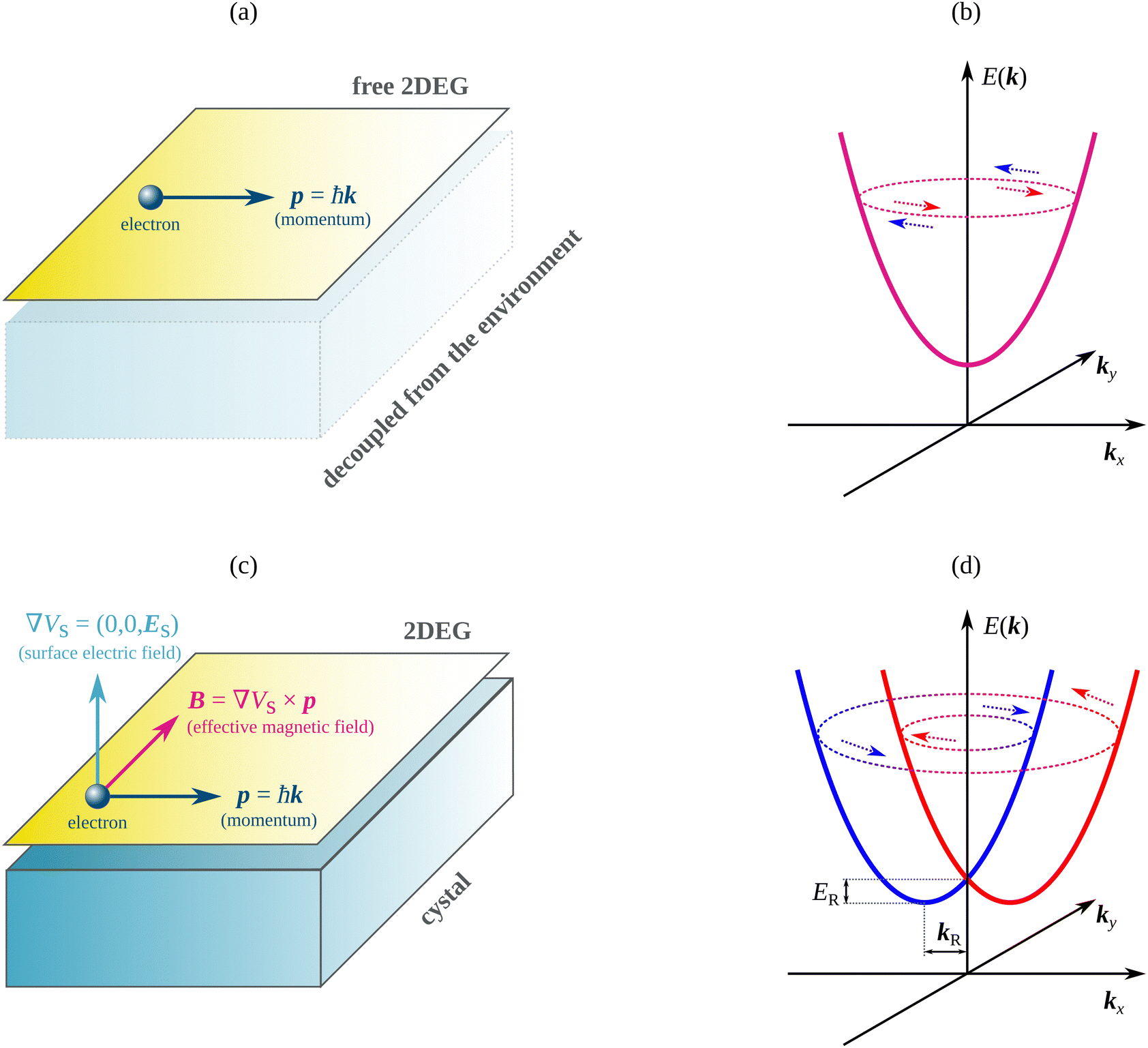 | ||
| Fig. 1 (a) Schematic representation of 2DEG decoupled from structural asymmetry environment. (b) Spin-degenerated band of 2DEG without ISB. (c) Schematic depiction of 2DEG in presence of a surface potential leading to ISB. (d) Momentum-dependent splitting of spin bands governed by the BR model in presence of ISB. | ||
Before addressing the common limitations of the RB model, it is important to note that the preceding discussion serves as an introductory-level overview of the model. As a result, extensive derivation or overwhelming mathematical formalism has been intentionally avoided, with the focus primarily on the fundamental principles and central features of the model. Readers interested in a more formal derivation are encouraged to explore the model within the framework of p·k perturbation theory.29 Additionally, it is worth mentioning that the crystal field does not significantly contribute to the Rashba effect in a manner that is relevant to understanding the model. Consequently, the discussion has omitted the crystal potential (Vbulk). However, if included, the main difference would be the utilization of the effective mass m*, and the split bands would be parabolic only in a local approximation.
3 Limitations of Bychkov–Rashba picture
The BR model qualitatively captures the effects observed experimentally, predicting both the spin splitting and the spin texture. However, despite its achievements, the model still presents several unresolved issues. First and foremost, the predicted energy scale of the band splitting is significantly underestimated for surfaces with GSS. The theoretical approximations of the Rashba coupling in the BR framework amount only to ∼10−3 meV Å, which would result in spin splitting much smaller than kBT at room temperature. Nevertheless, the experimentally observed effects on surfaces of Au25,30,31 or InSb32 demand values on the order of ∼100 meV Å, while in more extreme cases, such as Bi monolayers on Ag(001),33 the parameter can even exceed 3 eV Å. Hence, the quantitative estimates of αR from the BR model are orders of magnitude too small in the ideal 2DEG approach. In addition, GSS is known to favor high-atomic-number materials, which is not predicted by the BR model. For instance, αR for Au(111) is ten times larger than for Ag(111),34 despite comparable work functions between them, indicating that something is missing in this picture.Several arguments have been proposed to address these issues. Notably, some researchers have highlighted the importance of the product of charge density (ρ) and the potential gradient along the surface normal (∂V/∂z) as a critical factor governing the magnitude of Rashba spin splitting13,35
 | (6) |
 | ||
| Fig. 2 Schematic graph for potential gradient (blue) and charge density (yellow) along surface normal. Dashed line indicates an nuclei position. | ||
On the other hand, some researchers argue that the splitting energy arises from the strong in-plane gradient of the crystal field in the surface layer.28,36 Then, in cases with complex spin textures, others have explored the concept of the “extended” Rashba effect,37,38 which can be represented as
| ĤeR = ĤR + σ·Be(k) | (7) |
 | ||
| Fig. 3 Schematic illustration of the spin texture in k-space of some hexagonal system showing in-plane spin polarization around Γ and M points (fuchsia), and out-of plane polarization near K (red) and K′ (blue). | ||
The above-mentioned arguments have proven helpful for certain systems. However, they remain somewhat speculative as they alone cannot fully explain all aspects of Rashba-related phenomena, nor do they support a quantitative analysis required for further validation. Consequently, the predictive power of the BR picture remains limited, even when expanded. The BR model, represented by eqn (4), significantly underestimates spin splitting when the effect is substantial, and it does not allow for spin splittings exceeding a few meV. Thus, it does not provide valuable insights to guide the search for materials with desirable GSS.
Eqn (6) emphasizes the importance of charge asymmetry. However, the asymmetry of charge is intrinsic to all surfaces, while its interplay with potential gradient is not intuitively obvious based solely on the material composition or structure. As a result, this approach is more suited to explain already observed spin splittings rather than guiding the discovery of superior materials for spintronics.
Lastly, the extended Rashba model, given by eqn (7), explores the role of the surface. Nonetheless, even if its impact is acknowledged, the relationship between the effective magnetic field and the material symmetry is not intuitive and proves rather challenging to assess both qualitatively and quantitatively.†
Consequently, the BR picture has not been the driving force behind material development. Instead, extensive experimental work has demonstrated which types of structures are capable of supporting GSS, with the BR model adjusted to fit the results.
4 What a chemist ought to do?
GSS was first observed on Au(111),25 and subsequently on surfaces of other high-atomic-number materials, including Bi,39 Gd,40 and W.41 Furthermore, when compared the results have demonstrated a relation between the atomic number of the comprising elements and the magnitude of the splitting. Notably, the surfaces of Bi, which is the heaviest of non-radioactive elements, exhibit spin splittings as large as 300 meV, while on Au it is only ∼100 meV. Consequently, these experimental studies have established that, apart from Rashba SOI, GSS is somehow affected by atomic SOI, which contrasts the ideal 2DEG picture. Further research has shown that Bi monolayers induce even greater spin splitting on surfaces of Ag, on the order of 1 eV.28,33 Subsequently, similar effects have been reported for Tl, Pb, and Bi layers on semiconductor surfaces like Si(111)36,37,42 and Ge(111).13,43,44 Current research continues to explore the development of surface modifications.45–50 However, it also delves into GSS induced in novel 2D layered materials, including transition-metal dichalcogenides (TMDs),51–57 MXenes,58–63 and a variety of other sheets.64–72To facilitate the ongoing efforts, it is crucial to develop more robust strategies for enhancing spin splitting. Clear guiding principles need to be established to design materials with desired GSS. As a result, it becomes essential to thoroughly characterize and understand spin splitting in novel cases, such as on van der Waals (vdW) heterostructures,3,52,54,60,64,73 topological insulators,17,74,75 and Janus-type 2D materials.61,63,70,72 Additionally, structural modification of these novel platforms must be considered to unlock their full potential for spintronics applications.
As such, it would seem that chemists could play a crucial role in the search for new materials for spintronics due to their expertise in understanding and manipulating the properties of materials at the atomic and molecular levels. The chemical perspective could be particularly insightful in:
• Materials synthesis: chemists are skilled in designing and synthesizing various materials with specific properties. In spintronics, they can create new compounds or modify existing materials to optimize their electronic and magnetic properties, making them suitable for spintronic applications.
• Thin-film deposition techniques: spintronic devices frequently utilize thin films of materials with customized properties, and the understanding of chemical principles is pivotal in the effective use of dedicated techniques like chemical vapor deposition (CVD) or atomic layer deposition (ALD).
• Materials design and tailoring: by understanding the principles of chemical bonding and electronic structure, chemists can design and tailor materials with specific properties relevant to spintronics, such as strong spin–orbit coupling, long spin relaxation times, and high spin polarization.
• Quantum chemistry and computational modeling: chemists can use quantum chemistry calculations and computational modeling to predict the electronic and magnetic properties of materials. These techniques help in screening large databases of materials to identify promising candidates for spintronic applications.
However, what about a comprehensive characterization and deep insight into the mechanisms responsible for the arising spin splitting? Even if it occurs in new materials, without a well-described mechanism behind the splitting, the potential for developing more robust strategies for enhancing spin splitting will be limited despite the clear need for guiding principles in GSS engineering. Unfortunately, this is the aspect where many chemically-oriented investigations fall short.
In such cases, researchers often resort to using the BR picture to describe the effects of structural modification. Consequently, they fail to recognize the role of atomic SOI. Instead, the observed GSS is interpreted within the framework of a 2DEG model in accordance with eqn (4). However, since this approach cannot predict the energy scale of the band splitting, the model is usually supplemented with experimental or computational data to fit the model, i.e.,
 | (8) |
While still working in the BR framework, researchers could consider some of the proposed amendments. Consequently, the role of the interplay between charge density and the potential gradient along the surface normal could be highlighted. Still, it should be noted that Nagano et al.35 formulated the relation, given by eqn (6), for surface systems where broken bonding configuration results in asymmetric features of the surface state in the nucleus region, i.e., within one Bohr around the surface atom. Hence, when employed for the vdW interface, the argumentation should be used with care. Interestingly, both Nagano et al.35 and Sakamoto et al.37 have simultaneously discussed the abrupt rotation of the spin vector within the BR picture, emphasizing the role of the 2D hexagonal system of the surfaces on which it occurs. Hence, a similar approach could be adopted for modified TMDs as well as other p3m1 and p31m layers. Nevertheless, such argumentation may prove difficult, since it was shown that GSS for hexagonal systems can be enhanced or quenched for the same surfaces and adsorption layers depending only on the adsorption site of the latter.38,76
Hence, what can a chemist do in this situation? The BR framework is frequently used in material investigations, but it poses challenges when trying to account for the effects of chemical engineering. Additionally, it provides no guidance in the selection of structures and modifications. As a result, many researchers find themselves without the necessary tools to address the problems at hand and meaningfully contribute to the search for optimal materials for spintronic applications.
However, there exists an elegant and approachable solution to most of the highlighted problems. That is, to recognize the role of atomic SOI in the formation of GSS, and adopt the so-called orbital Rashba picture,77,78 where local orbital angular momentum (OAM) plays a crucial role in the effect. The rise of unquenched OAM via chemical functionalization can be easily understood, explored, and exploited. Therefore, it could be an optimal tool for chemists to investigate materials with GSS.
5 Orbital Rashba picture
To address the aforementioned limitations and gain a clear understanding of the orbital Rashba picture, let us consider an effective Hamiltonian of a bulk system, which includes three terms: | (9) |
 | (10) |
ĤSOI = ξ![[L with combining circumflex]](https://www.rsc.org/images/entities/b_i_char_004c_0302.gif) ·Ŝ, ·Ŝ, | (11) |
and Ŝ are the angular momentum and spin angular momentum operators, respectively. The fourth term is the Rashba Hamiltonian, ĤR, as given in eqn (3) and (4). Finally, the fifth term accounts for the interaction between the asymmetric charge distribution and the surface electrostatic field, which can be approximately expressed as:78–80| ĤEs = ·Es = β(k × Es)·, | (12) |
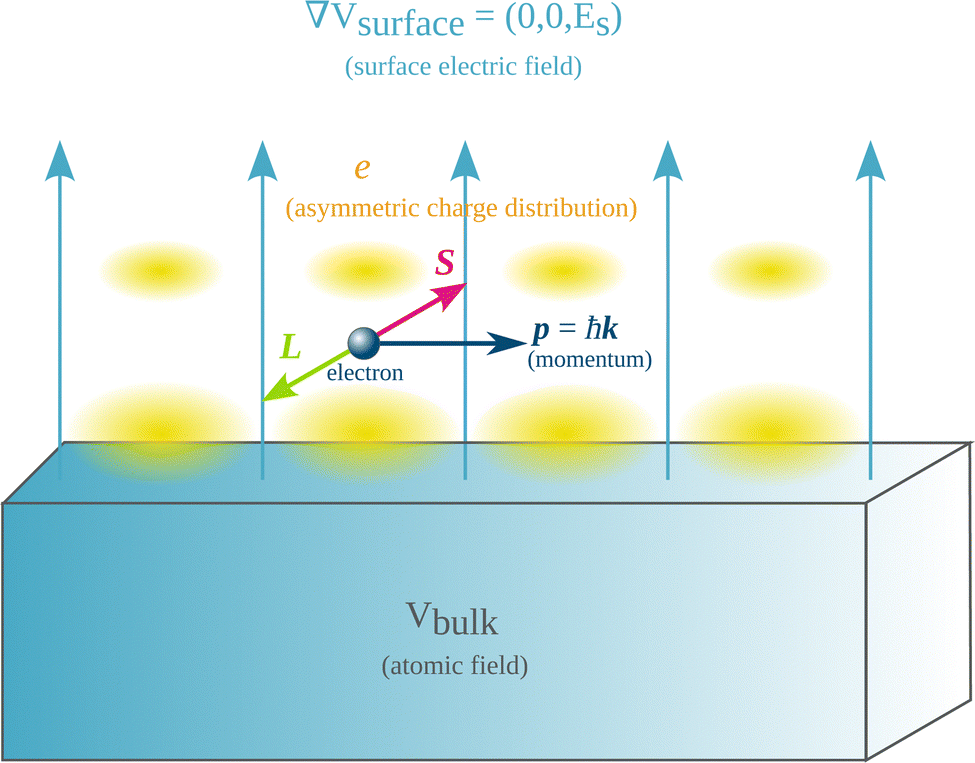 | ||
| Fig. 4 Schematic of the model system in the orbital picture of the spin splitting of surface bands. Electron (blue) has non-zero spin (fuchsia) and orbital angular momentum (lime) while moving in the presence of crystal and surface potentials. | ||
In this system, three terms from eqn (10) could potentially contribute to lifting spin degeneracy: ĤR, ĤSOI, and ĤEs. The influence of the Rashba SOI, as mentioned earlier, is generally negligible, leading to energy splittings of only a few meV. Conversely, atomic SOI for high-atomic-number elements can easily be on the order of 1 eV. Similarly, the electrostatic Hamiltonian can also facilitate the experimentally observed energy splitting scale, as p·Es ∼ eÅ × V/Å ∼ eV.78–80 Therefore, both new terms may contribute to the generation of GSS in the presence of non-vanishing OAM.
Box 1 Atomic orbitals and quantum numbersAtomic orbitals refer to one-electron wavefunctions that serve as quantum-mechanical solutions to the Schrödinger equation. They give distinct atomic energy levels for electrons to occupy, and they can be intuitively understood as electron clouds. Each orbital in an atom is characterized by a set of values, resulting in distinct electronic states. The principal quantum number (n) designates the main energy level of an atomic orbital, dictating its size and distance from the nucleus. The orbital (azimuthal) quantum number (l) delineates the orbital angular momentum and shape, resulting in different types of orbitals such as s, p, d, and f orbitals. The magnetic quantum number (ml) specifies the orientation of an orbital within a given energy level and shape, enabling differentiation of individual orbitals of the same type. The spin quantum number (ms) indicates the intrinsic spin of an electron within an orbital, highlighting its fundamental quantum property. |
As a result, the orbital picture attributes the band splitting to the rise of unfurnished OAM via atomic SOI and the interaction between the electrostatic field due to ISB and the asymmetric charge distribution. However, which term is dominant depends on the material, with those having strong SOI, such as Au(111), experiencing spin degeneracy predominantly lifted by ĤSOI (see Fig. 5a), while those with very strong coupling, like Bi2Te2Se, exhibiting splitting dominated by ĤEs (see Fig. 5b). Furthermore, as k is confined to the surface plane while Es is normal to it, ĤEs naturally couples in-plane OAM, resulting in a Rashba-type spin splitting. This leads to lifting the degeneracy by offsetting the bands in the momentum space around a TRIM point and complete spin polarization of the bands, with the spin polarization vectors exhibiting opposite directions for the two bands (see Fig. 6a). On the other hand, ĤSOI can couple both in-plane and out-of-plane spin. Consequently, it can also facilitate a Zeeman-type splitting (L·S ∼ σ·BSOI), where at a low-symmetry point bands are shifted on the energy scale depending on the spin polarization (see Fig. 6b).
 | ||
| Fig. 5 Schematic of energy levels with Rashba-type splitting for p states in the case of (a) strong and (b) very strong SOI. Red and blue arrows symbolize spin, while lime-colored arrows represent OAM. | ||
 | ||
| Fig. 6 Schematic depiction of the band structure and spin-texture of systems featuring the (a) Rashba and (b) Zeeman effects. The red and blue arrows indicate the orientation of spin polarization. | ||
Taken together, it is clear that optimizing GSS requires a keen understanding of the interplay between the atomic SOI, locking the SAM on the OAM direction, and the crystal field, which lifts the degeneracy of the OAM. That being said, it becomes imperative to delve into the mechanisms driving the emergence of non-vanishing orbital momentum in surface systems. Furthermore, we should explore the intricate connection between this phenomenon and the underlying chemical structure of materials.
6 Non-vanishing orbital momentum
Before delving into the intricacies of non-zero OAM in crystal structures, it's essential to first examine the behavior of OAM within isolated atoms and understand how it becomes suppressed within bulk materials. In free atoms, the OAM of electrons is well-defined and able to contribute significantly to the total angular momentum of the atom. Its non-zero values arise from the spherical potential generated by the atomic nuclei, i.e., Vatom ∼ 1/r, since the symmetry of this potential leads to constant values for the square of the OAM, as well as for one of its components (often represented as Lz), i.e.,| L2, Lz = const. | (13) |
| L2 = ħ2l(l + 1), | (14) |
| Lz = mlħ. | (15) |
So, how can we induce non-vanishing OAM within crystals? The short answer is: by mixing orthogonal orbitals, such that the hybrid is antisymmetric in momentum space.76–78 However, to delve deeper into this concept, let's once again consider a fictitious system. In Fig. 7a, an atomic chain is aligned along the x-axis, with each atomic site comprising px and py orbitals. Due to the chain's mirror symmetry plane running parallel to the xz plane, the px and py orbitals remain orthogonal to each other and decoupled,
| 〈px|Ĥ|py〉 = 〈py|Ĥ|px〉 = 0. | (16) |
| 〈px||py〉 = 〈py||px〉 = 0. | (17) |
〈px|Ĥ|py〉 = −2itpxpy![[thin space (1/6-em)]](https://www.rsc.org/images/entities/char_2009.gif) sin(ka), sin(ka), | (18) |
〉 = 〈pi||pj〉. Therefore, for the chosen geometry, the values of OAM at each atomic site will give| 〈x〉 = 〈y〉 = 0, | (19) |
| 〈z〉 ∼ tpxpysin(ka). | (20) |
| L(k) = −L(−k). | (21) |
 | ||
| Fig. 7 Symmetry breaking in an atomic chain giving rise to k-antisymmetric orbital momentum; (a) and (d) no ISB, (b) and (e) electrostatic symmetry breaking, and (c) and (f) geometric symmetry breaking. (a)–(c) Atomic sites comprising px and py orbitals. (d) and (f) Atomic sites comprising dx2−y2 and dxy orbitals. In panels (a) and (d), interatomic hopping energy between orbitals is zero owing to the presence of a mirror plane parallel to the xz plane. In panels (c), (c), (e), and (f), there is no mirror plane parallel to the xz plane, resulting in non-zero interatomic hopping between orbitals of differing parity. | ||
The very same mechanism applies seamlessly when transitioning from p-type to d-type orbitals. In the case of an atomic chain aligned along the x-axis with each atomic site comprising dx2−y2 and dxy orbitals (see Fig. 7d), the orbitals will be decoupled from each other, and they will form two bands with zero OAM. However, if this symmetry plane is broken (see Fig. 7e and f), the orbitals will become coupled, and 〈z〉 will be proportional to the interatomic hopping energy between dx2−y2 and dxy.
Naturally, these model examples are simple, providing only a glimpse into the myriad scenarios for inducing non-vanishing OAM. GSS has been observed in a wide range of materials. Hence, it would be prudent to delve into a selection of real examples. This endeavor will provide a more nuanced perspective, demonstrating how the aforementioned methodology can be applied effectively in practical situations.
7 Examples
In order to address a diverse range of relevant scenarios, this section examines GSS formation using real-world materials, including Au(111), Pb/Si(111)-1 × 1, MoS2, HgTe, and GaAs. These examples embody distinct material classes featuring GSS: a high-atomic-number metal surface, a semiconductor surface decorated with high-atomic-number elements, and a 2D sheet. Each of these selected materials holds significance in spintronics and presents a characteristic case of GSS formation that is representative of a specific class of structures.7.1 Au(111)
First, let's delve into the well-known Rashba-type splitting of Au(111), utilizing the orbital framework to elucidate the formation of the GSS. The surface states in this material encompass 6s, 6p, and 5d orbitals. At the Γ point, where symmetry dictates zero OAM and spin splitting, the states comprise decoupled s, pz, and dz2 orbitals. However, as we move from this high-symmetry point, surface effects come into play, leading to momentum-dependent intra-atomic orbital coupling. This interplay along the kx direction gives rise to mixing between pz/px and dz2/dxz orbitals. Conversely, coupling along ky involves pz/py and dz2/dyz orbitals, resulting in intermediate mixing at wavevectors in between. The differing parity of these coupled orbitals facilitates non-zero interatomic hopping energies between pz and px (py) orbitals (Fig. 8a), as well as between dz2 and dx (dyz) orbitals (Fig. 8b). | ||
| Fig. 8 Au(111) surface. Panels (a) and (b) illustrations depicting the interatomic hopping interactions between (a) pz and py orbitals, as well as (b) dz2 and dxy orbitals of the outermost layer of Au atoms on the surface. (c) Shows spin degenerated surface bands near Γ in the absence of SOI, with a notable chiral texture characterized by lime-colored arrows. (d) Illustrates the impact of SOI on the surface bands near the Γ point, showcasing Rashba-type splitting (blue and red colors indicate spin polarization). | ||
As we now know, the non-zero hopping energy gives rise to bands possessing non-zero OAM. Moreover, due to the momentum-dependent mixing, these interorbital hoppings induce a non-zero 〈y〉 along kx, and 〈x〉 along ky. Consequently, a chiral OAM structure emerges around the Γ point (depicted in Fig. 8c). This chiral OAM couples with a spin via atomic SOI, causing the spin to adopt in-plane polarization and circulate within momentum space around Γ (illustrated in Fig. 8d). In terms of the splitting magnitude, it is worth noting that the atomic SOI strength of the 6p orbitals is considerably smaller than that of the 5d orbitals in Au. Hence, the 5d orbitals will have a significant contribution to GSS. However, the splitting will not reach the same magnitude as the atomic SOI for 5d orbitals in Au, due to the surface states not being exclusively composed of 5d orbitals.
The described mechanisms driving GSS formation remain applicable to various other transition metals, albeit with some variation. In practical terms, the same fundamental principles underpinning the emergence of unquenched OAM are observed in Cu(111) and Ag(111), owing to the shared face-centered cubic (FCC) crystal structure and their membership in group 11. Nevertheless, due to substantial variations in their atomic SOI, only the surface of gold will exhibit GSS. In other cases, distinct crystal structures and electronic configurations of elements will yield diverse band structures, but still, a similar interplay between orbitals will govern the Rashba-type splitting on pristine surfaces of d-block elements.
7.2 Pb/Si(111)-1 × 1
Now, let's delve into the influence of surface bonding on GSS formation, which should hold particular relevance for chemists or individuals aiming to utilize chemical modifications of surfaces to facilitate GSS. To explore this, we will examine the intriguing case of Pb/Si(111)-1 × 1. In this structure, GSS at the K-point of its surface Brillouin zone can either be suppressed or enhanced, depending upon the specific adsorption site of Pb atoms.Silicon possesses a face-centered diamond-cubic crystal structure. Hence, when cleaved along the (111) plane, the resultant surface—assuming the absence of reconstruction (i.e., a 1 × 1 cell)—exhibits atoms arranged in a hexagonal symmetry. Within this arrangement, each double layer of silicon forms a buckled honeycomb structure, which is stacked with an AB–BC–CA sequence along the surface's normal direction. This stacking gives rise to three distinct adsorption sites within the 1 × 1 cell: T1, T4, and H3. These sites correspond to atoms adsorbed on top of the topmost, second, and fourth layer of silicon atoms, respectively. When Pb is adsorbed at site T1, it leads to a quenched spin splitting at the K-point. On the other hand, adsorption at sites T4, and H3 results in a GSS of ≈800 meV.38 As a result, for our discussion, we will focus on the T1 configuration (see Fig. 9a and b) and the H3 configuration (see Fig. 9d and e).
 | ||
| Fig. 9 Pb/Si(111)-1 × 1 surface configurations and electronic bands. Panels (a) and (b) Showcase side and top views of the T1 configuration, where Pb atoms reside above the topmost Si atoms. (c) Depicts the surface bands in the T1 configuration, featuring the px and py orbitals of Pb near the K-point. Notably, despite the substantial atomic SOI of Pb, the bands remain spin-degenerate, with predominantly in-plane orientation of the spin vector (there is no circular rotation of spin around K as it is not a TRIM point). (d) and (e) Present side and top views of the H3 configuration, with Pb atoms positioned above the fourth-layer Si atoms. (f) Illustrates the surface bands in the H3 configuration, again involving the px and py orbitals of Pb near the K point. Changing the adsorption site results in an abrupt rotation of the spin vector and a GSS of ≈800 meV. Panels (a) and (d) include a schematic representation of the Pb–Si bonding hybridization, while panels (b) and (e) highlight the px and py orbitals of Pb contributing to bonding in the adsorption layer, along with the mirror symmetry planes of the in-plane Pb hybrids (dashed lines). | ||
At first glance, the disparity in spin splitting between these configurations might appear puzzling, considering they occur on the same surface, decorated with the same elements arranged in identical patterns. Consequently, we are confronted with cases involving comparable surface potentials and identical atomic SOI. This, in itself, could pose a challenge when attempting to reconcile within the framework of the original Rashba model. However, given our understanding that orbital hybridization of surface states leads to non-vanishing OAM, it is reasonable to suspect that surface bonds affect the splitting depending on the orbitals they mix.
Upon closer examination, it becomes apparent that the bonding between Pb and Si in the T1 configuration involves the pz orbitals of both Pb and Si (see Fig. 9a). This leaves the px–py hybrids in the Pb layers mostly unaffected, effectively decoupling them from the structural asymmetry of the environment. As a result, despite the three-fold symmetry of the Si substrate, the six-fold symmetry of the px–py states of Pb remains intact. This, in turn, allows the monolayer to maintain mirror symmetry in the xz plane, preserving the relative parity of the px–py orbitals (see Fig. 9b). Consequently, the interatomic hopping energy between these orbitals along the x direction approximates zero. As a result, the px and py orbitals do not contribute to a non-zero 〈z〉 along the Γ–K path, leading to the absence of GSS at the K point (depicted in Fig. 9c).
In contrast, the bonding between Pb and Si in the H3 configuration once again involves the pz orbitals of Si, but this time, it includes the px and py orbitals of Pb (see Fig. 9d). This effectively breaks the six-fold symmetry within the px–py hybrids in the Pb layer, resulting in their loss of mirror symmetry in the xz plane (see Fig. 9e). Consequently, as these orbitals exhibit different parities with respect to the xz plane, the interatomic hopping energy between the px and py orbitals along the x direction assumes a non-zero value. This, in turn, gives rise to an unquenched 〈z〉 along the Γ–K path, which couples spin viaL·S, facilitating Zeeman-type splitting centered at the K point (shown in Fig. 9f). Given that the bands predominantly comprise Pb 6p orbitals, which are characterized by strong atomic SOI, this results in a significant GSS of ≈0.8 eV. Also, it is noteworthy that, since the hopping energy from px to py along the x direction carries an opposing sign compared to that in the −x direction, the polarization of spin is opposite between the K and K′ points.
The outlined mechanisms driving the formation of GSS can be considered as somewhat characteristic of p3m1 surfaces with decorations comprising high-atomic-number elements from the p-block. This is rooted in the fact that all px–pz and py–pz bonds disrupt the inherent six-fold symmetry of in-plane hybrids regardless of the elements comprising the surface. Consequently, if such bonds are formed, the resulting loss of symmetry enables px–py coupling to generate non-vanishing 〈z〉, with the extent of splitting predominantly contingent on the atomic SOI of the adsorbate. Consequently, this relationship between symmetry, surface bonding, and SOI has facilitated the same type of GSS in materials such as Tl/Si(111)-1 × 1,37 Pb/Ge(111)-1 × 1,76 Pb/germanene,65 and X/silicene (X = Tl, Pb, Bi).66
7.3 MoS2
Turning to our next example, let's shift our focus to the class of 2D layered materials, an area that has recently garnered significant attention within spintronics research.73,83–86 In this context, we will delve into hexagonal-phase transition-metal dichalcogenides (TMDs), which have piqued interest due to their novel properties. Notably, these materials stand out as semiconductors featuring GSS at the top of their valence band.87–91 Prominent examples of such TMDs encompass molybdenum disulfide (MoS2), molybdenum diselenide (MoSe2), molybdenum ditelluride (MoTe2), tungsten disulfide (WS2), and tungsten diselenide (WSe2). For our current purpose, we will focus on MoS2, given its status as one of the most extensively studied TMD sheets. Nevertheless, it is crucial to acknowledge that the same underlying mechanisms govern GSS within the other monolayers of this group. The MoS2 monolayer consists of three atomic layers, with a central layer of Mo sandwiched between two layers of S. Within the monolayer, Mo atoms favor sd5 hybridization, yielding a trigonal-prismatic bonding geometry. This arrangement imparts mirror symmetry to MoS2 monolayers at the plane containing Mo atoms—let's denote it as the xy plane (refer to Fig. 10a). Consequently, both 〈x〉 and 〈y〉 remain quenched, thereby precluding the formation of Rashba-type splitting around the Γ point despite the presence of the surface.
 | ||
| Fig. 10 MoS2 structure and electronic bands. Panel (a) illustrates the side view of the MoS2 monolayer with the xy mirror-symmetry plane indicated on the Mo layer. Panel (b) depicts the top views of MoS2, including three mirror-symmetry pains and schematics for an interatomic hopping between dxy and dx2−y2 orbitals of Mo along the x direction. Due to the lack of symmetry, the latter results in a Zeeman-type splitting at the K-point depicted in (c). Panels (d)–(f) showcase ISB of the xy mirror-symmetry plane via an external (d) electric field, (e) adsorption, and (f) Janus-type substitution, which can result in Rashba-type splitting near Γ-point as depicted in (g). | ||
Nonetheless, a Zeeman-type splitting does manifest at the K and K′ points, a phenomenon attributed to the lack of in-plane symmetry. To grasp this concept more comprehensively, let's inspect the structure of MoS2 in more detail. Upon examining the monolayer from a top-down perspective, an additional mirror plane emerges parallel to the yz plane (see Fig. 10b). Consequently, along the Γ–M line, 〈z〉 equates to zero, thus preventing any occurrence of spin splitting. However, as we move away from this line and explore k vectors that deviate from it, the absence of additional mirror symmetry becomes evident, allowing for 〈z〉 to exhibit non-zero values.
The split states at the valence band maximum are predominantly composed of dxy and dx2−y2 orbitals of Mo. Therefore, when we investigate the valence-band states with k directed along the Γ–K path in the kx direction, it becomes evident that 〈z〉 will be directly proportional to the interatomic hopping energy between these orbitals along the x direction, which is non-zero due to the presence of S ions. Subsequently, the non-zero OAM couples with spin via the strong atomic SOI of Mo's 4d orbitals, resulting in splitting governed by L·S, and spin polarization along the z direction (see Fig. 10c). Notably, these features of GSS concur with computational predictions and experimental findings for TMDs.51–57 Furthermore, owing to the distinct parities of these orbitals relative to the yz plane, the hopping energy from dxy to dx2−y2 along the x direction carries an opposing sign to that in the −x direction. Thus, as a natural consequence, the observed splitting along the Γ–K′ path exhibits reverse spin polarization—a characteristic feature inherent to hexagonal structures.
In the pursuit of material functionalization, it is important to recognize that Rashba-type splitting can also be induced in TMDs. Achieving this necessitates breaking the inherent xy mirror symmetry of the monolayer. This can be achieved through various means, such as applying an external electric field (depicted in Fig. 10d), adsorbing high-atomic-number elements (as illustrated in Fig. 10e), or utilizing Janus TMD—monolayers composed of a transition metal layer sandwiched between two distinct chalcogen atomic layers, for example, MoSSe (see Fig. 10f). In such cases, the absence of xy symmetry permits non-zero values for 〈x〉 and 〈y〉, which can have a significant impact on the GSS. In particular, electronic states of the highest valence band near the Γ point are known to be notably affected. With the xy symmetry intact, the band consists mostly of dz2 orbitals of Mo. However, in the presence of ISB, dz2 orbitals couple with dxz along the kx direction and with dyz along the ky direction. Notably, due to the distinct parity of the coupled orbitals in relation to the xy plane, the interatomic hopping energy between them becomes non-zero. This leads to the emergence of non-vanishing orbital OAM, characterized by 〈x〉 and 〈y〉, which in the presence of atomic SOI induces a Rashba-type splitting (see Fig. 10g).
7.4 HgTe and GaAs
Having covered both Rashba and Zeeman-type GSS, it would be prudent to conclude our examples by illustrating how the interorbital-hopping mechanism for non-zero OAM can be applied to Dresselhaus-type splitting in bulk systems.§ Much like the Rashba effect, this phenomenon results in the splitting of energy bands due to spin–orbit interaction in the presence of inversion asymmetry. However, unlike the Rashba effect, where asymmetry typically arises from the spatial inhomogeneity of an interface or surface, the Dresselhaus effect originates from the bulk's inversion asymmetry.92 With this distinction in mind, it is worth exploring whether such lack of symmetry can also induce non-zero OAM, whether these bands exhibit spin splitting, and if the extent of this effect is linked to the atomic SOI of the elements comprising the crystal structure.To illustrate this, we will examine the spin splitting of the lowest conduction band in bulk materials characterized by a zinc blende crystal structure. This choice is driven by the fact that zinc blende crystals lack the inversion symmetry required for Dresselhaus-type GSS, and their lowest conduction bands have orbital compositions suitable for the comparative analysis.
Let's begin our inquiry by examining a material comprised of high-atomic-number elements, such as mercury telluride (HgTe). The unit cell of HgTe is illustrated in Fig. 11a. HgTe is a semi-metal related to the II–VI group of semiconductors known for being the first discovered topological insulator.93 In the vicinity of the Γ point, the lowest conduction band of this material is primarily composed of 5s and 5p orbitals of Te.75 At the Γ point, where symmetry dictates zero OAM and spin splitting, the electronic states consist solely of s orbitals. However, as we move away from this high-symmetry point, crystal field effects come into play. These effects can lead to a momentum-dependent mixing of orthogonal p orbitals of Te, which, in principle, could result in non-zero OAM.
 | ||
Fig. 11 HgTe structure and electronic bands. Panel (a) illustrates the unit cell of the HgTe with (![[1 with combining macron]](https://www.rsc.org/images/entities/char_0031_0304.gif) 10) mirror plane is shaded in yellow. The Hg and Te atoms are colored as lime and dark blue, respectively. Panel (b) depicts a schematic representation of the interatomic hopping between px and py orbitals of Te along [110] direction. Panel (c) shows the spin splitting in the lowest conduction band of HgTe. GaAs structure and electronic bands. The Ga and As atoms are colored as fuchsia and jade, respectively. Panel (e) depicts a schematic representation of the interatomic hopping between px and py orbitals of As along [110] direction. Panel (f) shows the spin splitting in the lowest conduction band of GaAs. 10) mirror plane is shaded in yellow. The Hg and Te atoms are colored as lime and dark blue, respectively. Panel (b) depicts a schematic representation of the interatomic hopping between px and py orbitals of Te along [110] direction. Panel (c) shows the spin splitting in the lowest conduction band of HgTe. GaAs structure and electronic bands. The Ga and As atoms are colored as fuchsia and jade, respectively. Panel (e) depicts a schematic representation of the interatomic hopping between px and py orbitals of As along [110] direction. Panel (f) shows the spin splitting in the lowest conduction band of GaAs. | ||
Consequently, let's delve into the symmetries of the zinc blende structure and determine when and how will they affect the OAM. When the momentum vector k is aligned along the [100] direction the OAM and spin splitting in the lowest conduction band will remain zero due to the presence of two mirror planes, (011) and (01). Furthermore, the same will hold true for k aligned along the [010] and [001] directions. However, when k is aligned along the [110] direction (for convenience, let's refer to it as the x direction), the (10) plane is the only mirror plane containing the [110] direction. The (001) plane is not a mirror plane due to the presence of Hg atoms positioned above Te atoms, as shown in Fig. 11a. This broken mirror symmetry causes the pz–px hybrid orbitals to be antisymmetric in momentum space, as depicted in Fig. 11b. This leads to non-zero OAM oriented in the [10] (lets refer to it as the y direction), 〈y〉, which couples spin via strong atomic SOI of Te, contributing to non-zero spin splitting along [110] (kx), as shown in Fig. 11c. Meanwhile, when k is along [10], the arrangement of Hg atoms below Te atoms in the Hg–Te zigzag chain along [10] changes the sign of the hopping energy between pz and py orbitals. This reversal in sign results in a change in the OAM direction, making the OAM dependent on the k direction.
However, what would happen if the atomic SOI was weaker? Would this result in a lower value of spin splitting? Let's explore this by considering a material composed of lower-atomic-number elements compared to HgTe, such as gallium arsenide (GaAs). GaAs is a well-known III–V semiconductor, but it should be noted that other related compounds like InP or InAs could have been considered instead. The lower conduction band of GaAs exhibits a similar dispersion compared to that of HgTe.75,94 At the Γ point, this band comprises s orbitals of Ga and As. However, due to the crystal structure (refer to Fig. 11d), the same symmetries apply as in the case of HgTe. Hence, along the [110] direction, the crystal field induces momentum-dependent mixing of orthogonal p orbitals, mainly of As origin (as shown in Fig. 11e) Consequently, this leads to a non-zero OAM, which coincides with the spin splitting along the [110] direction. as shown in Fig. 11f. Nevertheless, the atomic SOI in As is weaker compared to Te. As a result, this splitting in GaAs is relatively lower when compared to HgTe.75,94 Furthermore, a similar argument applies when comparing the splitting along the [110] direction in GaAs and GaSb. In GaSb, the stronger SOI of Sb contributes to a greater magnitude of spin splitting.94
8 Giant spin splitting without spin–orbit interaction
In our final comments, it is important to emphasize that not all GSS phenomena are solely a result of strong atomic SOI. In fact, SOI is not a necessary condition for achieving an antisymmetric spin texture in momentum space. The crucial factor is the disruption of rotational symmetry, which ensures that SAM is no longer a conserved quantum number. Apart from SOI, magnetism can also disrupt spin rotational invariance.95,96 This exchange-induced momentum-dependent spin splitting has been observed in various intrinsic collinear antiferromagnetic materials.97,98 It is also well established that GSS can be obtained via exchange interaction with magnetic impurities or magnetic layers in semiconductor materials.74,99–101 In these compounds, electron spins align with the magnetic order, making them distinct from the SOI-induced splitting discussed in this review (see discussion elsewhere19). Since the chemical composition of these materials also plays a significant role in the formation of GSS, there could be a substantial area of research that pertains to chemical physicists in this field. To achieve a momentum-dependent spin texture, characterized by variations in spin direction across the Brillouin zone, one should consider (antiferro)magnetic materials with non-collinear magnetic structures.102 The resulting spin texture exhibits symmetries consistent with the underlying magnetic configuration and remains inversion-symmetric. When spatial inversion symmetry is broken in antiferromagnets, it gives rise to antisymmetric spin-momentum locking, as discussed elsewhere.1039 Conclusions
To facilitate the ongoing efforts in the field of spintronics, it is crucial to devise more robust strategies for enhancing spin splitting. Clear guiding principles need to be established to design materials with desired GSS. As a result, it becomes essential to thoroughly characterize and understand spin splitting in new materials. Furthermore, structural modification of these novel platforms must be considered to unlock their full potential for spintronics applications. This endeavor, in turn, captures the interest of numerous young chemists, who, due to the lack of necessary tools, often struggle to accurately account for the atomic SOI in the formation of GSS. This is often facilitated by the interpretation of the spin splitting derived from the original Bychkov–Rashba picture. The model predicts, among other things, spin-degeneracy lifting with a chiral spin structure. However, it fails the predicted energy scale of the band splitting, since it does not consider contributions from atomic SOI.The role of atomic SOI in the formation of GSS has been well established, paving the way for a more informed exploration of materials with desired spin properties. This exploration often involves taking into consideration the effects of OAM and accounting for its generation. However, since non-vanishing OAM is frequently elucidated within tight-bonding models, its emergence may seem sometimes perplexing or even daunting to grasp for many young researchers interested in spintronics and material research.
Nevertheless, this complexity can be demystified. The most straightforward method to generate an atomic orbital moment involves mixing orthogonal orbitals in the presence of ISB, ensuring that the hybrid is antisymmetric in momentum space. Consequently, by understanding the nature of chemical bonding in the materials, coupled with consideration for the symmetry of the system, and orbital parity, ample insight can be gained into the mechanisms underlying the formation of non-vanishing OAM.
Furthermore, this perspective distinctly highlights that surface interactions hold a substantial significance in facilitating spin splitting. Depending on the specific orbitals involved, these interactions can either suppress or enhance GSS. This insight proves particularly useful for new materials and chemical modification, as it establishes an intuitive connection between GSS and chemical bonding in the presence of ISB, sufficient to understand the mechanism behind non-zero OAM, without the explicit reliance on the tight-binding Hamiltonian. Consequently, this approach can render it more approachable to understand, explore, and exploit the effects of atomic SOI when designing novel materials for spintronics.
Author contributions
Maciej J. Szary: conceptualization, formal analysis, investigation, writing – original draft, writing – review & editing, visualization, supervision, project administration.Conflicts of interest
There are no conflicts to declare.Acknowledgements
This work was supported by the Ministry of Education and Science in Poland (Grant No. 0512/ SBAD/2320) within the project realized at the Institute of Physics, Poznan University of Technology.Notes and references
- M. Atzori and R. Sessoli, J. Am. Chem. Soc., 2019, 141, 11339–11352 CrossRef CAS PubMed.
- D. Akinwande, C. Huyghebaert, C.-H. Wang, M. I. Serna, S. Goossens, L.-J. Li, H.-S. P. Wong and F. H. L. Koppens, Nature, 2019, 573, 507–518 CrossRef CAS PubMed.
- S.-J. Liang, B. Cheng, X. Cui and F. Miao, Adv. Mater., 2020, 32, 1903800 CrossRef CAS PubMed.
- V. Saraswat, R. M. Jacobberger and M. S. Arnold, ACS Nano, 2021, 15, 3674–3708 CrossRef CAS PubMed.
- S. A. Wolf, D. D. Awschalom, R. A. Buhrman, J. M. Daughton, S. von Molnár, M. L. Roukes, A. Y. Chtchelkanova and D. M. Treger, Science, 2001, 294, 1488–1495 CrossRef CAS PubMed.
- S. A. Wolf, A. Y. Chtchelkanova and D. M. Treger, IBM J. Res. Dev., 2006, 50, 101–110 CAS.
- S. Bhatti, R. Sbiaa, A. Hirohata, H. Ohno, S. Fukami and S. Piramanayagam, Mater. Today, 2017, 20, 530–548 CrossRef.
- A. Hirohata, K. Yamada, Y. Nakatani, I.-L. Prejbeanu, B. Diény, P. Pirro and B. Hillebrands, J. Magn. Magn. Mater., 2020, 509, 166711 CrossRef CAS.
- X. Wang, Z. Cheng, G. Zhang, H. Yuan, H. Chen and X.-L. Wang, Phys. Rep., 2020, 888, 1–57 CrossRef CAS.
- Y. Huang, V. Polojärvi, S. Hiura, P. Höjer, A. Aho, R. Isoaho, T. Hakkarainen, M. Guina, S. Sato, J. Takayama, A. Murayama, I. A. Buyanova and W. M. Chen, Nat. Photonics, 2021, 15, 475–482 CrossRef CAS.
- M. Ramsteiner, O. Brandt, T. Flissikowski, H. T. Grahn, M. Hashimoto, J. Herfort and H. Kostial, Phys. Rev. B: Condens. Matter Mater. Phys., 2008, 78, 121303 CrossRef.
- M. Gurram, S. Omar and B. J. V. Wees, Nat. Commun., 2017, 8, 248 CrossRef CAS PubMed.
- K. Yaji, Y. Ohtsubo, S. Hatta, H. Okuyama, K. Miyamoto, T. Okuda, A. Kimura, H. Namatame, M. Taniguchi and T. Aruga, Nat. Commun., 2010, 1, 17 CrossRef PubMed.
- H. C. Koo, S. B. Kim, H. Kim, T.-E. Park, J. W. Choi, K.-W. Kim, G. Go, J. H. Oh, D.-K. Lee, E.-S. Park, I.-S. Hong and K.-J. Lee, Adv. Mater., 2020, 32, 2002117 CrossRef CAS PubMed.
- K. Yasuda, H. Yasuda, T. Liang, R. Yoshimi, A. Tsukazaki, K. S. Takahashi, N. Nagaosa, M. Kawasaki and Y. Tokura, Nat. Commun., 2019, 10, 2734 CrossRef PubMed.
- Y. M. Itahashi, T. Ideue, Y. Saito, S. Shimizu, T. Ouchi, T. Nojima and Y. Iwasa, Sci. Adv., 2020, 6, eaay9120 CrossRef PubMed.
- J. B. S. Mendes, M. Gamino, R. O. Cunha, J. E. Abrão, S. M. Rezende and A. Azevedo, Phys. Rev. Mater., 2021, 5, 024206 CrossRef CAS.
- S. Varotto, L. Nessi, S. Cecchi, J. Sławińska, P. Noël, S. Petrò, F. Fagiani, A. Novati, M. Cantoni, D. Petti, E. Albisetti, M. Costa, R. Calarco, M. Buongiorno Nardelli, M. Bibes, S. Picozzi, J.-P. Attané, L. Vila, R. Bertacco and C. Rinaldi, Nat. Electron., 2021, 4, 740–747 CrossRef CAS.
- G. Bihlmayer, P. Noël, D. V. Vyalikh, E. V. Chulkov and A. Manchon, Nat. Rev. Phys., 2022, 4, 642–659 CrossRef.
- A. Manchon, H. C. Koo, J. Nitta, S. M. Frolov and R. A. Duine, Nat. Mater., 2015, 14, 871–882 CrossRef CAS PubMed.
- D. Bercioux and P. Lucignano, Rep. Prog. Phys., 2015, 78, 106001 CrossRef PubMed.
- M. S. Bahramy and N. Ogawa, Adv. Mater., 2017, 29, 1605911 CrossRef PubMed.
- T. Uchihashi, AAPPS Bull., 2021, 31, 27 CrossRef.
- Y. A. Bychkov and E. I. Rashba, JETP Lett., 1984, 39, 78–81 Search PubMed.
- S. LaShell, B. McDougall and E. Jensen, Phys. Rev. Lett., 1996, 77, 3419–3422 CrossRef CAS PubMed.
- M. Hoesch, M. Muntwiler, V. N. Petrov, M. Hengsberger, L. Patthey, M. Shi, M. Falub, T. Greber and J. Osterwalder, Phys. Rev. B: Condens. Matter Mater. Phys., 2004, 69, 241401 CrossRef.
- D. Pacilé, C. R. Ast, M. Papagno, C. Da Silva, L. Moreschini, M. Falub, A. P. Seitsonen and M. Grioni, Phys. Rev. B: Condens. Matter Mater. Phys., 2006, 73, 245429 CrossRef.
- C. R. Ast, J. Henk, A. Ernst, L. Moreschini, M. C. Falub, D. Pacilé, P. Bruno, K. Kern and M. Grioni, Phys. Rev. Lett., 2007, 98, 186807 CrossRef PubMed.
- T. Oguchi and T. Shishidou, J. Phys.: Condens. Matter, 2009, 21, 092001 CrossRef PubMed.
- A. Nuber, J. Braun, F. Forster, J. Minár, F. Reinert and H. Ebert, Phys. Rev. B: Condens. Matter Mater. Phys., 2011, 83, 165401 CrossRef.
- S. N. P. Wissing, C. Eibl, A. Zumbülte, A. B. Schmidt, J. Braun, J. Minár, H. Ebert and M. Donath, New J. Phys., 2013, 15, 105001 CrossRef.
- G. A. Khodaparast, R. E. Doezema, S. J. Chung, K. J. Goldammer and M. B. Santos, Phys. Rev. B: Condens. Matter Mater. Phys., 2004, 70, 155322 CrossRef.
- T. Nakagawa, O. Ohgami, Y. Saito, H. Okuyama, M. Nishijima and T. Aruga, Phys. Rev. B: Condens. Matter Mater. Phys., 2007, 75, 155409 CrossRef.
- K. Yaji, A. Harasawa, K. Kuroda, R. Li, B. Yan, F. Komori and S. Shin, Phys. Rev. B, 2018, 98, 041404 CrossRef CAS.
- M. Nagano, A. Kodama, T. Shishidou and T. Oguchi, J. Phys.: Condens. Matter, 2009, 21, 064239 CrossRef PubMed.
- I. Gierz, T. Suzuki, E. Frantzeskakis, S. Pons, S. Ostanin, A. Ernst, J. Henk, M. Grioni, K. Kern and C. R. Ast, Phys. Rev. Lett., 2009, 103, 046803 CrossRef CAS PubMed.
- K. Sakamoto, T. Oda, A. Kimura, K. Miyamoto, M. Tsujikawa, A. Imai, N. Ueno, H. Namatame, M. Taniguchi, P. E. J. Eriksson and R. I. G. Uhrberg, Phys. Rev. Lett., 2009, 102, 096805 CrossRef PubMed.
- B. Pieczyrak, M. Szary, L. Jurczyszyn and M. W. Radny, Phys. Rev. B, 2016, 93, 195318 CrossRef.
- Y. M. Koroteev, G. Bihlmayer, J. E. Gayone, E. V. Chulkov, S. Blügel, P. M. Echenique and P. Hofmann, Phys. Rev. Lett., 2004, 93, 046403 CrossRef PubMed.
- O. Krupin, G. Bihlmayer, K. Starke, S. Gorovikov, J. E. Prieto, K. Döbrich, S. Blügel and G. Kaindl, Phys. Rev. B: Condens. Matter Mater. Phys., 2005, 71, 201403 CrossRef.
- M. Hochstrasser, J. G. Tobin, E. Rotenberg and S. D. Kevan, Phys. Rev. Lett., 2002, 89, 216802 CrossRef CAS PubMed.
- M. H. Berntsen, O. Götberg and O. Tjernberg, Phys. Rev. B, 2018, 97, 125148 CrossRef CAS.
- S. Hatta, T. Aruga, Y. Ohtsubo and H. Okuyama, Phys. Rev. B: Condens. Matter Mater. Phys., 2009, 80, 113309 CrossRef.
- S. Hatta, T. Aruga, C. Kato, S. Takahashi, H. Okuyama, A. Harasawa, T. Okuda and T. Kinoshita, Phys. Rev. B: Condens. Matter Mater. Phys., 2008, 77, 245436 CrossRef.
- A. V. Matetskiy, S. Ichinokura, L. V. Bondarenko, A. Y. Tupchaya, D. V. Gruznev, A. V. Zotov, A. A. Saranin, R. Hobara, A. Takayama and S. Hasegawa, Phys. Rev. Lett., 2015, 115, 147003 CrossRef CAS PubMed.
- K. Taguchi, K. Sumida, Y. Okuda, K. Miyamoto, A. Kimura, T. Oguchi and T. Okuda, Phys. Rev. B, 2020, 101, 045430 CrossRef CAS.
- W. Ju, D. Wang, T. Li, Y. Zhang, Z. Gao, L. Ren, H. Li and S. Gong, Phys. Chem. Chem. Phys., 2020, 22, 9148–9156 RSC.
- L. Chi, C. V. Singh and J. Nogami, Nanoscale, 2021, 13, 16622–16628 RSC.
- A. Mihalyuk, L. Bondarenko, A. Tupchaya, T. Utas, J.-P. Chou, D. Gruznev, S. Eremeev, A. Zotov and A. Saranin, Nanoscale, 2022, 14, 11227–11234 RSC.
- S. Zhang, F. Wang, B. Cui, C. Li and Y. Jia, Phys. Lett. A, 2023, 479, 128920 CrossRef CAS.
- S. Oh and H. J. Choi, Sci. Rep., 2017, 7, 2024 CrossRef PubMed.
- M. J. Szary, M. T. Michalewicz and M. W. Radny, Appl. Surf. Sci., 2019, 494, 619–626 CrossRef CAS.
- L. Yuan, Q. Liu, X. Zhang, J.-W. Luo, S.-S. Li and A. Zunger, Nat. Commun., 2019, 10, 906 CrossRef PubMed.
- S. Gupta and B. I. Yakobson, J. Am. Chem. Soc., 2021, 143, 3503–3508 CrossRef CAS PubMed.
- F. Sattari and S. Mirershadi, Sci. Rep., 2021, 11, 17617 CrossRef CAS PubMed.
- Q. Peng, Y. Lei, X. Deng, J. Deng, G. Wu, J. Li, C. He and J. Zhong, Phys. E, 2022, 135, 114944 CrossRef CAS.
- F. Sattari, J. Phys. Chem. Solids, 2023, 182, 111567 CrossRef CAS.
- H. Lind, J. Halim, S. I. Simak and J. Rosen, Phys. Rev. Mater., 2017, 1, 044002 CrossRef.
- R. Meshkian, H. Lind, J. Halim, A. El Ghazaly, J. Thörnberg, Q. Tao, M. Dahlqvist, J. Palisaitis, P. O. A. Persson and J. Rosen, ACS Appl. Nano Mater., 2019, 2, 6209–6219 CrossRef CAS.
- H. U. Din, M. Idrees, A. Albar, M. Shafiq, I. Ahmad, C. V. Nguyen and B. Amin, Phys. Rev. B, 2019, 100, 165425 CrossRef CAS.
- S.-D. Guo, W.-Q. Mu, Y.-T. Zhu, R.-Y. Han and W.-C. Ren, J. Mater. Chem. C, 2021, 9, 2464–2473 RSC.
- D. Ghosh, K. Roy, S. Maitra and P. Kumar, J. Phys. Chem. Lett., 2022, 13, 1234–1240 CrossRef CAS PubMed.
- C. Xin, Z. Fan, Z. Sun, H. Li, G. Jin, F. Pan and Y. Sui, Phys. Chem. Chem. Phys., 2023, 25, 8676–8683 RSC.
- W. Wei, Y. Dai, C. Niu, X. Li, Y. Ma and B. Huang, J. Mater. Chem. C, 2015, 3, 11548–11554 RSC.
- M. J. Szary, FlatChem, 2019, 18, 100141 CrossRef CAS.
- M. J. Szary, Surf. Sci., 2020, 697, 121604 CrossRef CAS.
- S. B. Touski and N. Ghobadi, J. Phys. D: Appl. Phys., 2021, 54, 485302 CrossRef CAS.
- D. Fang, S. Chen, Y. Li and B. Monserrat, J. Phys.: Condens. Matter, 2021, 33, 155001 CrossRef CAS PubMed.
- Y. Li, X. Xu, M. Lan, S. Wang, T. Huang, H. Wu, F. Li and Y. Pu, Phys. Chem. Chem. Phys., 2022, 24, 25962–25968 RSC.
- Y. Li, M. Lan, S. Wang, T. Huang, Y. Chen, H. Wu, F. Li and Y. Pu, Phys. Chem. Chem. Phys., 2023, 25, 15676–15682 RSC.
- N. Li, Q. Xia, W.-X. Ji, M. Ding, M.-J. Ren, P.-J. Wang, P. Li, S.-F. Zhang and S.-S. Li, Phys. E, 2023, 148, 115654 CrossRef CAS.
- B. D. Bhat, J. Phys.: Condens. Matter, 2023, 35, 435301 CrossRef PubMed.
- A. M. Hoque, V. Ramachandra, A. George, E. Najafidehaghani, Z. Gan, R. Mitra, B. Zhao, D. Khokhriakov, A. Turchanin, S. Lara-Avila, S. Kubatkin and S. P. Dash, Phys. Rev. Mater., 2023, 7, 044005 CrossRef CAS.
- Y. G. Semenov, X. Duan and K. W. Kim, Phys. Rev. B: Condens. Matter Mater. Phys., 2012, 86, 161406 CrossRef.
- R. Islam, B. Ghosh, G. Cuono, A. Lau, W. Brzezicki, A. Bansil, A. Agarwal, B. Singh, T. Dietl and C. Autieri, Phys. Rev. Res., 2022, 4, 023114 CrossRef CAS.
- M. J. Szary, B. Pieczyrak, L. Jurczyszyn and M. W. Radny, Appl. Surf. Sci., 2019, 466, 224–229 CrossRef CAS.
- S. R. Park, C. H. Kim, J. Yu, J. H. Han and C. Kim, Phys. Rev. Lett., 2011, 107, 156803 CrossRef PubMed.
- B. Kim, P. Kim, W. Jung, Y. Kim, Y. Koh, W. Kyung, J. Park, M. Matsunami, S.-I. Kimura, J. S. Kim, J. H. Han and C. Kim, Phys. Rev. B: Condens. Matter Mater. Phys., 2013, 88, 205408 CrossRef.
- J.-H. Park, C. H. Kim, J.-W. Rhim and J. H. Han, Phys. Rev. B: Condens. Matter Mater. Phys., 2012, 85, 195401 CrossRef.
- B. Kim, C. H. Kim, P. Kim, W. Jung, Y. Kim, Y. Koh, M. Arita, K. Shimada, H. Namatame, M. Taniguchi, J. Yu and C. Kim, Phys. Rev. B: Condens. Matter Mater. Phys., 2012, 85, 195402 CrossRef.
- L. Petersen and P. HedegÅrd, Surf. Sci., 2000, 459, 49–56 CrossRef CAS.
- M. Kim, J. Im, A. J. Freeman, J. Ihm and H. Jin, Proc. Natl. Acad. Sci. U. S. A., 2014, 111, 6900–6904 CrossRef CAS PubMed.
- C. K. Safeer, J. Ingla-Aynés, F. Herling, J. H. Garcia, M. Vila, N. Ontoso, M. R. Calvo, S. Roche, L. E. Hueso and F. Casanova, Nano Lett., 2019, 19, 1074–1082 CrossRef CAS PubMed.
- J. Ingla-Aynés, F. Herling, J. Fabian, L. E. Hueso and F. Casanova, Phys. Rev. Lett., 2021, 127, 047202 CrossRef PubMed.
- F. Calavalle, M. Suárez-Rodríguez, B. Martín-García, A. Johansson, D. C. Vaz, H. Yang, I. V. Maznichenko, S. Ostanin, A. Mateo-Alonso, A. Chuvilin, I. Mertig, M. Gobbi, F. Casanova and L. E. Hueso, Nat. Mater., 2022, 21, 526–532 CrossRef CAS PubMed.
- J. Ingla-Aynés, I. Groen, F. Herling, N. Ontoso, C. K. Safeer, F. de Juan, L. E. Hueso, M. Gobbi and F. Casanova, 2D Mater., 2022, 9, 045001 CrossRef.
- N. Alidoust, G. Bian, S.-Y. Xu, R. Sankar, M. Neupane, C. Liu, I. Belopolski, D.-X. Qu, J. D. Denlinger, F.-C. Chou and M. Z. Hasan, Nat. Commun., 2014, 5, 4673 CrossRef CAS PubMed.
- Y. Zhang, H. Li, H. Wang, R. Liu, S.-L. Zhang and Z.-J. Qiu, ACS Nano, 2015, 9, 8514–8519 CrossRef CAS PubMed.
- S. C. de la Barrera, M. R. Sinko, D. P. Gopalan, N. Sivadas, K. L. Seyler, K. Watanabe, T. Taniguchi, A. W. Tsen, X. Xu, D. Xiao and B. M. Hunt, Nat. Commun., 2018, 9, 1427 CrossRef PubMed.
- M. J. Szary, Appl. Surf. Sci., 2019, 491, 469–477 CrossRef CAS.
- H. Nakamura, A. Mohammed, P. Rosenzweig, K. Matsuda, K. Nowakowski, K. Küster, P. Wochner, S. Ibrahimkutty, U. Wedig, H. Hussain, J. Rawle, C. Nicklin, B. Stuhlhofer, G. Cristiani, G. Logvenov, H. Takagi and U. Starke, Phys. Rev. B, 2020, 101, 165103 CrossRef CAS.
- G. Dresselhaus, Phys. Rev., 1955, 100, 580–586 CrossRef CAS.
- M. König, S. Wiedmann, C. Brüne, A. Roth, H. Buhmann, L. W. Molenkamp, X.-L. Qi and S.-C. Zhang, Science, 2007, 318, 766–770 CrossRef PubMed.
- M. Gmitra and J. Fabian, Phys. Rev. B, 2016, 94, 165202 CrossRef.
- L.-D. Yuan, Z. Wang, J.-W. Luo, E. I. Rashba and A. Zunger, Phys. Rev. B, 2020, 102, 014422 CrossRef CAS.
- L.-D. Yuan, Z. Wang, J.-W. Luo and A. Zunger, Phys. Rev. Mater., 2021, 5, 014409 CrossRef CAS.
- L. Šmejkal, R. González-Hernández, T. Jungwirth and J. Sinova, Sci. Adv., 2020, 6, eaaz8809 CrossRef PubMed.
- R. González-Hernández, L. S. Šmejkal, K. Výborný, Y. Yahagi, J. Sinova, T. C. V. Jungwirth and J. Z. Železný, Phys. Rev. Lett., 2021, 126, 127701 CrossRef PubMed.
- T. Dietl, H. Ohno and F. Matsukura, Phys. Rev. B: Condens. Matter Mater. Phys., 2001, 63, 195205 CrossRef.
- J. A. Gaj and J. Kossut, in Basic Consequences of sp-d and d-d Interactions in DMS, ed. J. A. Gaj and J. Kossut, Springer Berlin Heidelberg, Berlin, Heidelberg, 2010, pp. 1–36 Search PubMed.
- T. Dietl and H. Ohno, Rev. Mod. Phys., 2014, 86, 187–251 CrossRef CAS.
- J. Z. Železný, Y. Zhang, C. Felser and B. Yan, Phys. Rev. Lett., 2017, 119, 187204 CrossRef PubMed.
- S. Hayami, Y. Yanagi and H. Kusunose, Phys. Rev. B, 2020, 101, 220403 CrossRef CAS.
Footnotes |
†  ; see ref. 37 for details. ; see ref. 37 for details. |
| ‡ Parity, also known as inversion, indicates whether an orbital exhibits symmetry or antisymmetry when subjected to an inversion operation. |
| § As mentioned earlier, the effective Hamiltonian in the BR model includes components in the form of (σxky − σykx). However, in cases where the system exhibits higher symmetry (e.g., in bulk), additional terms emerge, leading to the manifestation of the Dresselhaus effect. It's important to emphasize that the point-group symmetry is determined by the subgroup of the k-point. Consequently, the precise relationship between spin and crystal momentum hinges on the specific symmetry characteristics of the crystal. |
| This journal is © the Owner Societies 2023 |