
 Open Access Article
 This Open Access Article is licensed under a
 Creative Commons Attribution 3.0 Unported Licence
Interfacial interactions of doped-Ti3C2 MXene/MAPbI3 heterostructures: surfaces and the theoretical approach†
Muhammad Abiyyu Kenichi
Purbayanto
 a,
Arramel
*b,
See Wee
Koh
cd,
Francesco
Maddalena
d,
Dorota
Moszczyńska
a,
Jessie
Manopo
e,
Yudi
Darma
*ef,
Dominik
Kowal
g,
Hong
Li
cd,
Muhammad Danang
Birowosuto
*g and
Agnieszka Maria
Jastrzębska
*a
a,
Arramel
*b,
See Wee
Koh
cd,
Francesco
Maddalena
d,
Dorota
Moszczyńska
a,
Jessie
Manopo
e,
Yudi
Darma
*ef,
Dominik
Kowal
g,
Hong
Li
cd,
Muhammad Danang
Birowosuto
*g and
Agnieszka Maria
Jastrzębska
*a
aFaculty of Materials Science and Engineering, Warsaw University of Technology, Wołoska 141, 02-507 Warsaw, Poland. E-mail: agnieszka.jastrzebska@pw.edu.pl
bNano Center Indonesia, Jalan Raya PUSPIPTEK, South Tangerang, Banten 15314, Indonesia. E-mail: arramel@nano.or.id
cSchool of Mechanical and Aerospace Engineering, Nanyang Technological University, 639798, Singapore
dCINTRA CNRS/NTU/THALES, UMI 3288, Research Techno Plaza, 637553, Singapore
eDepartment of Physics, Institut Teknologi Bandung, Jalan Ganesa No. 10, Bandung 40132, Indonesia. E-mail: yudi@itb.ac.id
fResearch Collaboration Center for Quantum Technology 2.0, Bandung 40132, Indonesia
gŁukasiewicz Research Network—PORT Polish Center for Technology Development, Stabłowicka 147, 54-066 Wrocław, Poland. E-mail: muhammad.birowosuto@port.lukasiewicz.gov.pl
First published on 17th November 2023
Abstract
The work function (WF) of perovskite materials is essential for developing optoelectronic devices enabling efficient charge transfer at their interfaces. Perovskite's WF can be tuned by MXenes, a new class of two-dimensional (2D) early transition metal carbides, nitrides, and carbonitrides. Their variable surface terminations or the possibility of introducing elemental dopants could advance perovskites. However, the influence of doped-MXenes on perovskite materials is still not fully understood and elaborated. This study provides mechanistic insight into verifying the tunability of MAPbI3 WF by hybridizing with fluorine-terminated Ti3C2Tx (F-MXene) and nitrogen-doped Ti3C2Tx (N-MXene). We first reveal the interfacial interaction between MAPbI3 and MXenes via X-ray photoelectron spectroscopy (XPS), ultraviolet photoelectron spectroscopy (UPS), and photoluminescence spectroscopy (PL). UPS supported by density functional theory (DFT) calculations allowed the description of the influence of F and N on MXene's WF. Furthermore, we developed MAPbI3/MXene heterostructures using F- and N-MXenes. The F-MXenes extended the most WF of MAPbI3 from 4.50 eV up to 3.00 eV, compared to only a small shift for N-MXene. The underlying mechanism was charge transfer from low WF F-MXene to MAPbI3, as demonstrated by PL quenching in MAPbI3/F-MXene heterostructures. Altogether, this work showcases the potential of fluorine-doped MXenes over nitrogen-doped MXenes in advancing perovskite heterostructures, thus opening a door for efficient optoelectronic devices.
1. Introduction
Hybrid organic–inorganic perovskites are promising materials for applications in photovoltaic devices due to their high efficiency, low fabrication cost, bandgap tunability, and excellent optical absorption.1 One of their critical parameters is the work function (WF). Perovskite's WF is an essential parameter for tuning band alignment and charge transfer at materials interfaces, realizing a high photovoltaic device performance.2 Notably, WF can be tuned by two-dimensional (2D) materials such as MXenes.MXenes are a novel family of 2D materials called early transition metal carbides, nitrides, and carbonitrides. They are represented by the Mn+1XnTx (n = 1–4) chemical formula, in which M is a transition metal, and X denotes carbon or nitrogen. Tx refers to functional groups present on MXene surfaces, such as O, OH, and F,3 making MXenes highly dispersible in water and suitable for solution processing methods.4 MXenes exhibit remarkable physical properties, such as outstanding electrical conductivity (> 2.0 × 10⁴ S cm−1),5 high carrier density (3.8 × 1022 cm−3),6 and exceptional carrier mobility (1 cm2 V−1 s−1).6 MXene's optoelectronic properties become even more attractive due to their tunability. For instance, MXene's band structure can be altered by changing the transition metal's chemical structure or modifying the surface via functionalization.7
Introducing different surface terminations can control the WF of Ti3C2Tx MXene.8,9 These experimental findings were confirmed through density functional theory (DFT) calculations, which predicted that the WF of Ti3C2Tx MXene spans a broad energy range from 1.6 eV (–OH termination) to 6.25 eV (–O termination).10,11 Agresti et al. demonstrated the tunability of perovskite's WF by introducing MXene surface-terminated with –F, –OH, and –O functional groups.12 Incorporating the Ti3C2(OH)2 MXene reduced WF of MAPbI3 from 4.72 eV to 4.37 eV. The decrease of WF was induced by the dipole interaction and band alignment at the vicinity of the MAPbI3/Ti3C2(OH)2 interface, while the power conversion efficiency of MXene-modified perovskite reached 26%.12 Given the importance of tuneable WF in device fabrication, this behaviour is particularly promising when combined in a heterostructure assembly. WF tuning plays an essential role in the development of optoelectronic devices. The palette of approaches includes improving the charge transfer capability, constructing Schottky barriers, and determining the catalytic surface activity.13,14
MXenes have also been utilised as functional building blocks for optically active heterostructures.15–18 MXene-based heterostructures were developed for various applications, including photocatalysts,15 photodetectors,16 and photovoltaics.19 For instance, adding Ti3C2Tx to MAPbI3 facilitates more efficient electron transfer through the grain boundary.20 Furthermore, several researchers demonstrated other advantages of coupling Ti3C2Tx MXene with perovskites, such as robust optical absorption,21 WF alignment,12 controlled nucleation and crystallization of perovskites,19 and their efficient charge carrier transportation.22
Elemental doping of MXenes with non-metallic elements could enhance electrical conductivity, providing excellent WF tunability.23,24 However, an interplay between doped-MXene and perovskite in terms of the electronic structure and WF tuning is still not fully understood, although non-metallic doped MXenes already showed promising results in various opto- and electrochemical properties. For instance, by introducing nitrogen doping into Ti3C2Tx MXene lattices, the electrical conductivity and electron concentration of Ti3C2Tx can be increased compared with pristine Ti3C2Tx.25 Furthermore, nitrogen-doped Ti3C2Tx displayed a remarkable performance as an electrode for supercapacitor applications. An improvement of specific capacitance of 460% compared to the pristine led to excellent cyclic stability after 10![[thin space (1/6-em)]](https://www.rsc.org/images/entities/char_2009.gif) 000 charge and discharge cycles.25,26 In microwave absorbing applications, nitrogen doping can be a suitable alternative for magnetic nanoparticle fillers in Ti3C2Tx, which are susceptible to oxidation even at room temperature (RT).27
000 charge and discharge cycles.25,26 In microwave absorbing applications, nitrogen doping can be a suitable alternative for magnetic nanoparticle fillers in Ti3C2Tx, which are susceptible to oxidation even at room temperature (RT).27
However, mechanisms responsible for the interaction between surface-terminated or doped MXenes and perovskites are still not fully understood, especially in their influence on perovskite's electronic structure and WF. Hence, in this study, we aim to investigate the effect of fluorine termination and nitrogen doping of Ti3C2Tx on interfacial interactions with MAPbI3 perovskite. We have synthesized F-terminated Ti3C2Txvia conventional HF etching while N-doped Ti3C2Tx through thermal annealing. We further deposited MAPbI3 on MXene surfaces via a spin-coating technique and verified their optoelectronic properties and WF for F-MXene/MAPbI3 and N-MXene/MAPbI3 heterostructures.
Results from ultraviolet photoelectron spectroscopy (UPS), X-ray photoelectron spectroscopy (XPS), and photoluminescence spectroscopy (PL) showed that F-termination and N-doping significantly alter the WF of MAPbI3. MXenes effectively tuned the band alignment and interfacial charge transfer in MXene/perovskite heterostructures, which could enhance the optoelectronic device performance. Additionally, performed DFT calculations further supported our experimental findings.
This work demonstrates the potential of non-metal element additives to MXenes as a promising approach for developing high-performance MXene/perovskite heterostructures. Our study provides new insight into the heterostructure design of perovskite-based optoelectronic devices.
2. Materials and methods
2.1. Synthesis of Ti3C2Tx MXene
Ti3C2Tx MXene was synthesized by selective etching of the Ti3AlC2 MAX phase (Y-carbon Ukraine) with 48 wt% water solution of hydrofluoric acid (Sigma Aldrich, 695068). The 5-day etching process ensured complete etching out of aluminium and allowed high fluorine saturation of the MXene surface. After etching, MXene flakes were washed with distilled water (6000 rpm for 20 min) until the pH reached around 6. Then, MXene was dried overnight in a vacuum oven at 60 °C.2.2. Synthesis of F-terminated and N-doped MXene
In order to delaminate MXene, previously etched MXene powders with high fluorine saturation (0.3 grams) were sonicated in methanol for 60 min. Next, the delaminated MXene was centrifuged at 3500 rpm for 10 min to separate MXene from methanol. The sediment was further dried to collect MXene powders. As the MXene powders were highly functionalized by fluorine, we called it F-MXene in the entire paper. The dried MXene was then separated into different alumina crucibles for use in a tube furnace. Nitrogen-doped MXene (N-MXene) was acquired via thermal annealing 100 mg of as-etched MXene at 200 °C for 7 hours under a constant flow (10 sccm) of 10% ammonia in argon (10% NH3:90% Ar, Air Products). Au on Si and Si/SiO2 substrates were used to compare the physicochemical properties of MXene in different electronic environments. The powders of F-MXene and N-MXene were further dispersed in methanol and drop-casted on 100 nm-thick Au on Si or Si/SiO2 substrates.
2.3. MAPbI3 thin film fabrication
Perovskite thin films were deposited on previously prepared MXene on the top of 100 nm-thick Au on Si or Si/SiO2 substrates. Hereafter, the prepared films were denoted as the MAPbI3/MXene heterostructure. The perovskite solution was prepared by dissolving MAI and PbI2 with a molar ratio of 1:1 in N,N-dimethylformamide (DMF) (0.5 M) and stirred at 100 °C until complete dissolution. The MAPbI3 thin film was prepared by spin-casting a precursor solution on the top of MXene samples at 2000 rpm (acceleration = 500 rpm) for 30 s and blow-drying with N2 during the last 15 s when the sample was spinning, giving a thickness of ∼500 nm. The thin film was then placed on the surface of a hot plate and annealed at 100 °C for 15 min. MAPbI3 was relatively stable within humidity and the sample could withstand ∼1 week in the open air. However, the measurement was performed using the as-received sample (same day) to avoid damaging the samples.
2.4. Morphology and structural characterization
The as-prepared Ti3C2Tx (F-MXene) powder morphology was characterized using field-emission scanning electron microscopy (FESEM) of Hitachi S5500, Japan. Moreover, the morphology of F-MXene and N-MXene thin films was characterized using FESEM JEOL JSM-7600F, Japan. The micrographs were taken at an accelerating voltage of 6 kV in the secondary electron mode. The crystal structures of the Ti3AlC2 MAX phase and Ti3C2Tx were studied using a Bruker D8-Advance X-ray diffractometer (Cu Kα −0.154056 nm). The entire experiment was carried out at RT.2.5. XPS and UPS measurements
XPS experiments were carried out using an X-ray source of Magnesium Kα with a typical excitation energy output of 1254 eV. The XPS spectra were fitted using the Shirley background. UPS measurements were performed using a VG ESCA Lab system, an ultrahigh vacuum (UHV) system with a typical base pressure in the range of ∼10−10 mbar equipped with a gas discharge lamp in which helium gas was passed into the analysis chamber. The UV source was an unfiltered He Iα (21.2 eV) excitation, and the sample was biased at −5 V to extract the low-energy secondary electron cut-off (SECO). The UV light spot size on the sample is about 1 mm in diameter. All the reported photoemission spectra were calibrated by referencing the Ag 3d5/2 peak position (centered at 368.10 eV) of silver polycrystalline foil cleaned by standard argon ion sputtering treatment. The errors of all given values of binding energies and SECO positions are estimated to be ±0.05 eV.2.6. Steady state and dynamic PL measurements
We used a standard micro-PL setup at RT using free-space excitation.28 The samples were excited with a picosecond-pulsed ytterbium fiber laser emitting at 266 ± 2 nm and 532 ± 2 nm wavelength with a repetition rate of 10 MHz. The emission was observed through a 0.65-numerical-aperture visible-near-infrared microscope objective, by which the beam diameter was estimated to be 1 μm. PL spectra were recorded using an AvaSpec-HSC1024x58TEC-EVO spectrometer. Time-resolved (TR-) PL measurements were carried out using single-photon counting detector modules from Micro Photon Devices connected to the single-photon counting acquisition module (TCC900, Edinburgh Instruments). We filtered the emission with a bandpass filter at 450 ± 25 nm or a long pass filter at 650 nm.2.7. Computational methods
Theoretical calculations were carried out using the Quantum ESPRESSO (QE) package.29 We employed an exchange–correlation functional developed by Perdew–Zunger30 and the scalar-relativistic ultrasoft pseudopotential. The pseudopotential was chosen similar to the previous calculation.12 We used a Monkhorst–Pack k-point mesh of 7 × 7 × 1 and a plane wave basis set cutoff of 60 Ry based on our optimization, as shown in Fig. S1 (ESI†). About ∼10 Å vacuum was added within all calculations to the MXene structure to avoid the interaction with its image in the z-direction. The F and N surface terminations were added according to the previous report.8 The work functions were calculated from the electrostatic potential calculated using the pp.x code in QE. The obtained electrostatic potential was further averaged in the z direction using the average from the x code in QE to obtain the work function.We further performed N-doped Ti3C2Tx MXene calculation using a 3 × 3 × 1 supercell, where one of the carbon atoms was replaced by a nitrogen atom. The adsorption sites of –F and –OH were chosen to be face-centred cubic (FCC) and hexagonal closed-packed (HCP), respectively, owing to the most energetically favourable configurations.
3. Results and discussion
MXene nanoflakes were prepared by etching the parental Ti3AlC2 MAX phase in 48 wt% aqueous HF solution. In this study, the etching process was done for five days to ensure the fluorine species fully terminated MXene. The synthesized F-MXene showed characteristic few-to-multilayered flakes (Fig. 1(a)) with a typical accordion-like open structure (Fig. S2, ESI†).31,32 The X-ray diffraction pattern confirmed the successful preparation of Ti3C2Tx MXene (F-MXene), as evidenced by broader XRD peaks and the absence of the corresponding Ti3AlC2 patterns (Fig. 1(b)).33 Additionally, no diffraction patterns of TiO2 were observed, implying the high quality of synthesized Ti3C2Tx MXenes. Energy dispersive X-ray spectroscopy (EDS) analysis showed the presence of Ti, C, F, and O elements, with a negligible amount of Al (Fig. S3, ESI†). Interestingly, we obtained a high amount of F elements, suggesting dominant F-termination on the F-MXene surface, as we hypothesized before (Table S1, ESI†). After performing the nitrogen doping process, the surface morphology of MXene remains intact, as shown in Fig. S4 (ESI†).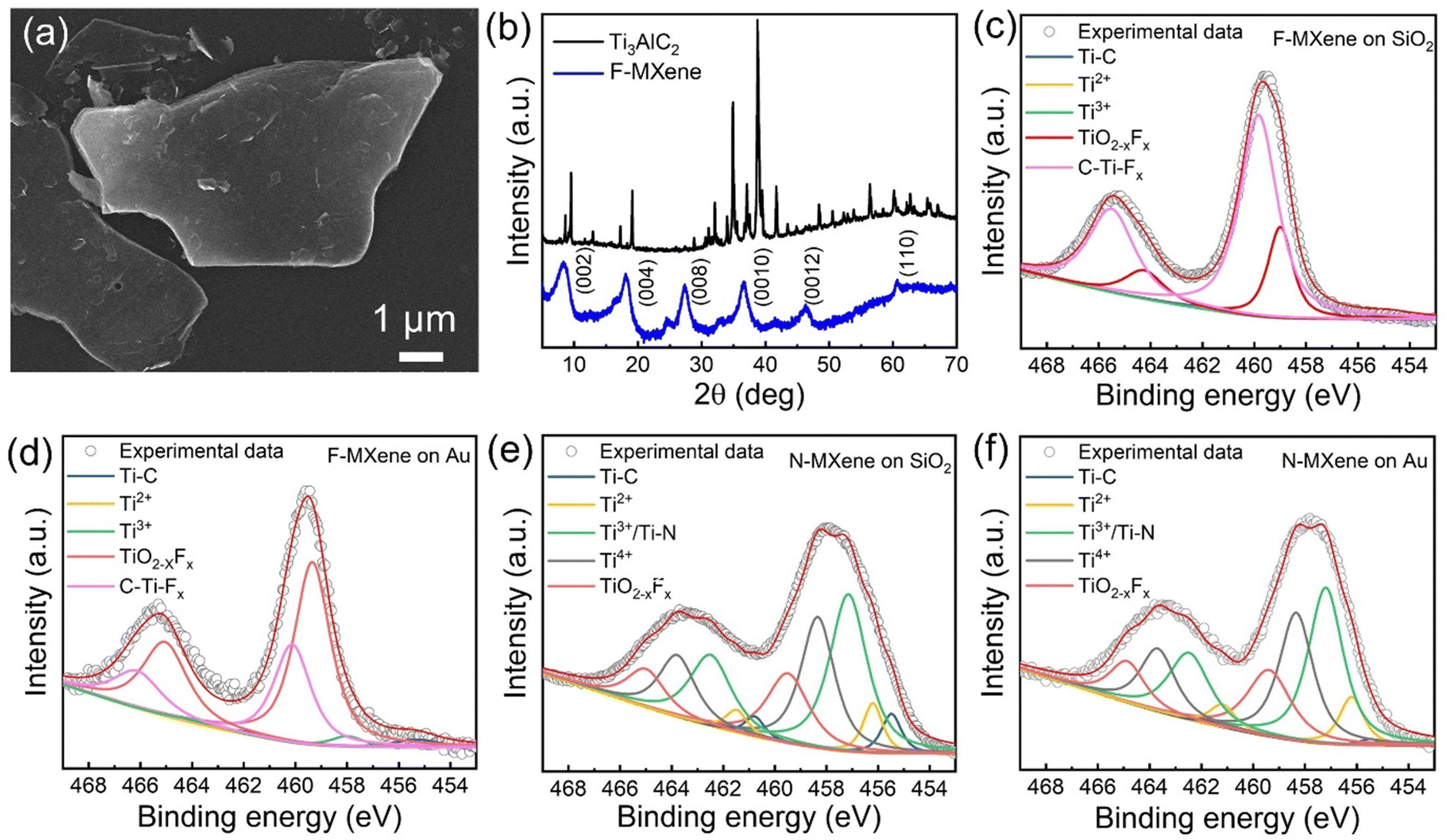 | ||
| Fig. 1 (a) Scanning electron microscopy (SEM) images of as-synthesized F-MXene. (b) X-ray diffractogram of the Ti3AlC2 MAX phase and as-synthesized F-MXene. Ti 2p fitted X-ray photoelectron spectroscopy (XPS) components of (c) F-MXene on SiO2, (d) F-MXene on Au, (e) N-MXene on SiO2, and (f) N-MXene on Au. | ||
We further conducted XPS analysis to study the chemical composition of F-MXene and N-MXene drop-casted on SiO2 and Au substrates. XPS survey spectra (Fig. S5, ESI†) revealed the presence of Ti, C, and O in both F-MXene and N-MXene. In addition, F-MXene exhibited a strong fluorine signal, indicating successful fluorine surface termination, which aligns with EDS results. We detected the presence of nitrogen in the XPS survey spectra of N-MXene, indicating the successful introduction of nitrogen doping. In addition, we analysed each of the XPS survey spectra of the samples in a similar route as outlined by Deeva et al.34 The elemental quantification of the F (N) to metal ratio of the respective samples are presented in Fig. S6 (ESI†). By comparing the area of F 1s and Ti 2p peaks, we unravel that the F/Ti ratio yields a high concentration of ca. 1.49 when the as-prepared F-MXenes were introduced onto the Au substrate. Our analysis here is in agreement with the previous report by Halim et al.35 strengthening the fact that F has the dominant fraction of termination groups for Ti-based MXenes. Interestingly, a reasonable concentration (0.42) was achieved when these doped-MXenes were deposited onto SiO2. In the case of N-MXene samples, we find a slightly reduced N/Ti ratio (0.17) on SiO2 and (0.18) on Au. Based on this recent investigation, each of the Tx surface group functionalization in Ti3C2Tx samples shows a contrasting atomic concentration profile of F(or N) species with respect to its metal constituent (Ti). The information regarding the ratio between F (N) and Ti could be further utilised to model MXene terminated locally by F or N. We envision that this will give a more precise local dipole distribution and detailed analysis of the Tx species role as demonstrated by Schultz et al.8 and Gouveia et al.36
The fitted Ti 2p XPS peaks of F-MXene deposited on SiO2 (Fig. 1(c)) and Au (Fig. 1(d)) showed the presence of diverse Ti components, including Ti–C (455.3 eV), Ti2+ (456.3 eV), Ti3+ (458 eV), TiO2−xFx (459.35 eV), and C–Ti–Fx (460.12 eV).35,37 In this regard, the fluorine-related species, i.e., TiO2−xFx and C–Ti–Fx, are observed to be present in substantial amounts. It is important to note that the value of the oxide component in F-MXene is located at a higher binding energy than pure TiO2 oxides (∼458.6 eV), indicating that the formed TiO2 is majorly doped/terminated with F atoms.37 This finding is reasonable as the HF etching process was performed for 5 days, resulting in high –F coverage on the surface of Ti3C2Tx.
In the case of N-MXene, nitrogen doping causes a redshift of the Ti 2p spectra. The redshifting suggests that the chemical environment of N-MXene differs from that of F-MXene. The fitted Ti 2p XPS spectra of N-MXene on SiO2 and Au are presented in Fig. 1(e) and (f), respectively. Ti 2p XPS spectra of N-MXene can be fitted into five different components, consisting of Ti–C (455.48 eV), Ti2+ (456.2 eV), Ti3+/Ti–N (457.15 eV), TiO2 (458.34 eV), and TiO2−xFx (459.49 eV).23 In contrast to F-MXene, N-MXene showed a significant contribution of Ti3+/Ti–N, implying that nitrogen atoms substitute titanium atoms in the MXene crystal lattice.23 These findings suggest that the chemical composition and oxidation states of MXene can be effectively tuned through doping, which can significantly impact various applications, including optoelectronic devices.
Fig. S7 (ESI†) presents the O 1s XPS spectra of F-MXene and N-MXene, providing insight into the functional groups on the respective surfaces. For F-MXene, the spectra show the contribution from TiO2 (529.8 eV), C–Ti–Ox (531.7 eV), and C–Ti–(OH)x (532.7 eV). Therefore, the XPS core levels of O 1s and Ti 2p confirm that F-MXene is successfully functionalized with the mix of –F, –OH, and –O functional groups. On the other hand, O 1s XPS spectra of N-MXene are fitted by TiO2 (529.8 eV), C–Ti–(OH)x (532.3 eV), and N–O (534.5 eV). In contrast to F-MXene, N-MXene is majorly terminated by the –OH functional group. Additionally, N–O suggests partial nitrogen incorporation within the surface functional groups.38 Nonetheless, we also observe a minor contribution of the –F functional group on N-MXene, which we will discuss further through XPS F 1s analysis.
Fig. S8 (ESI†) shows the F 1s XPS spectra of F-MXene and N-MXene. Here, F-MXene spectra can be fitted into three components, including C–Ti–Fx (684.6 eV), TiO2−xFx (685.2 eV), and AlFx (686.2 eV). The presence of the AlFx component is attributed to the by-product generated during the etching process.35 On the other hand, N-MXene spectra show two components, namely C–Ti–Fx (684.1 eV) and Al(OF)x (688.3 eV), with the latter originating from the synthesised by-product. Moreover, we emphasize that the –F terminated related species account for only a small fraction of N-MXene. In contrast, F-MXene exhibits a high amount of –F terminated Ti3C2Tx, indicating the rich surface fluorine (–F) termination on the MXene surface.
To further explore the nature of nitrogen doping in N-MXene, we move to the N 1s core level of XPS spectra. The fitted N 1s XPS spectra of N-MXene (Fig. S9, ESI†) exhibit a significant contribution from Ti–N (396.5 eV),39 with a minor contribution from O–Ti–N (397.3 eV)40 components. The presence of Ti–N in both Ti 2p and N 1s XPS spectra confirms the successful lattice substitution of C atoms with N atoms in the Ti3C2Tx structure.25,38 Furthermore, O–Ti–N can be connected to the decoration of nitrogen on the surface functional groups. Therefore, in our study, in addition to nitrogen substituting carbon atoms, as indicated by the Ti–N component, nitrogen also decorated the MXene surface, as demonstrated by the O–Ti–N XPS component.
Following the successful synthesis of F-MXene and N-MXene, we fabricated the MAPbI3/MXene heterostructure. To achieve this, thin film layers of MXene and MAPbI3 were prepared on SiO2 and the Au substrate using the spin-coating technique. Fig. 2(a) provides a schematic illustration of the fabrication process of the MAPBI3/MXene heterostructure. In particular, MAPbI3 layers were spin-coated on as-fabricated MXene layers. The heterostructured films show similar thicknesses (around 2 μm) as measured in MXene and MAPbI3 alone. This observation could be attributed to the consistency of the films obtained from the MXene drop-casting process and the deposited films’ relatively thick nature. Tilted SEM images of F-MXene, MAPbI3, and MAPbI3/MXene thin films deposited on the SiO2 substrate are displayed in Fig. 2(b)–(e). The SEM images confirm that the perovskite film well penetrated into MXene layers. Interestingly, upon MAPbI3 deposition on the MXene surface, the morphology of the thin film shows a smooth layer. This is attributed to the role of functional groups on the MXene surface in ensuring uniform blending between MXene and perovskite without introducing any aggregation. Furthermore, the EDS mapping of the heterostructured film (Fig. S10, ESI†) confirmed the presence of both Ti3C2Tx and MAPbI3.
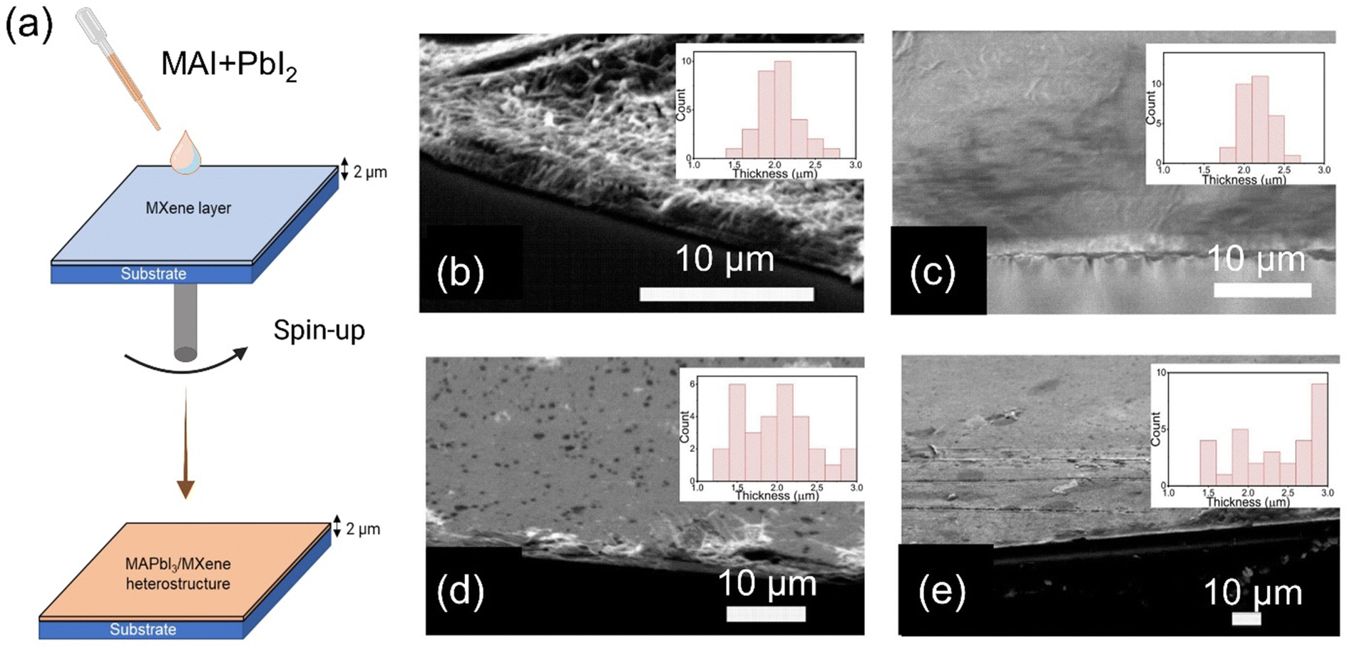 | ||
| Fig. 2 (a) Schematic diagram of the MAPbI3/MXene heterostructure fabrication procedure. Tilted cross-sectional SEM images of (b) F-MXene, (c) MAPbI3, (d) N-MXene/MAPbI3, and (e) F-MXene/MAPbI3 thin films deposited on the SiO2/Si substrate. The inset shows the thickness distribution of the films. All thicknesses are about 2 μm, indicating perovskite layers were well penetrated to the MXene structure. | ||
We further performed XPS measurements to probe the chemical composition of the MAPbI3/MXene heterostructured thin film. XPS spectra of MAPbI3/N-MXene and MAPbI3/F-MXene grown on SiO2 and Au substrates are presented in Fig. S11–S14 (ESI†). All the samples show C 1s, N 1s, O 1s, Ti 2p, Pb 4f, and I 3d XPS signals. Pb 4f shows symmetrical doublet peaks corresponding to the spin–orbit splitting of Pb 4f7/2 and 4f5/2 components from the Pb2+ cation in the MAPbI3 crystal structure.41 We do not observe any Pb 4f components located at a lower binding energy, indicating that no metallic Pb is formed during the perovskite preparation.42 Furthermore, the I 3d core level shows a single doublet peak, originating from 3d5/2 and 3d3/2, showing that only a single I component was observed in the film. Besides the contribution of I 3d and Pb 4f signals, we also observe the N 1s core level, which is related to the MA+ of the MAPbI3 structure.43 As MAPbI3 is deposited on the surface of MXene, the absence of the Ti 2p signal suggests that MAPbI3 effectively covers the MXene surface. Thus, our XPS analysis confirms the successful fabrication of an MAPbI3/MXene heterostructured thin film.
Using the UPS technique, we investigate the electronic structure of the MAPbI3/MXene heterostructure. First, we analysed the SECO region of F-MXene and N-MXene without perovskite addition, as presented in Fig. 3(a). We found that the extracted WF of F-MXene deposited on SiO2 and Au are 3.62 and 3.68 eV, respectively. The WF of both samples only shows slight shifting between each other, which is still in the experimental error range of the measurement. Furthermore, WFs of N-MXene on SiO2 and Au are estimated to be 4.22 and 4.30 eV. Here, we notice a slight shift (0.08 eV) in the WF of N-MXene when different substrates were used. Based on the previous studies, the variation of the WF value can be attributed to the interface dipole and band bending effect at the film/substrate interface,44,45 and functional groups present on the MXene surface.8 However, in our case, the former can be neglected, considering the probing depth of UPS is about 2–3 nm46 and our films have a thickness of 2 μm. Based on the study by Tamulewicz et al. the substrate effects on WF become important when we go down to the single or few-layer scale.47 Thus, we can conclude that there is a variation in surface functional groups present in N-MXene grown on Au and SiO2 substrates, leading to a slight difference in WF.
 | ||
| Fig. 3 (a) Secondary electron cut-off (SECO) signals of N-MXenes on Au (black) and SiO2 (red), F-MXenes on Au (blue), and SiO2 (green). The extracted work functions (WFs) are presented in the inset. (b) The valence band spectra of MXenes were recorded in various substrates and their corresponding extracted valence band maxima are shown in the inset. (c) Plane averaged electrostatic potential of F-MXene face-centred cubic (FCC) and (d) N-MXene hexagonal closed-packed (HCP) (zero referenced as the Fermi energy). | ||
It is important to note that the WF of Ti3C2Tx MXene strongly depends on the surface functional groups determined by the synthesis procedure.8,12 Based on the DFT result, the calculated WF of bare Ti3C2 is 5.05 eV.48 Moreover, the UPS determined WF of Ti3C2Tx obtained by HF etching, as reported in different works is 4.42 eV49 and 4.90 eV.50 Thus, the WF of our N-MXene and F-MXene thin films are relatively low compared to the previously calculated WF of Ti3C2Tx, implying that F and N atoms may act as n-dopants in the Ti3C2Tx structure. Next, we analyse the valence band region of F-MXene and N-MXene, as depicted in Fig. 3(b). The spectra show the intensity starting from the Fermi energy and peaking at a binding energy value of around 10 eV. It is worth noting that in the case of F-MXene, the intensity is relaxed compared to N-MXene.
To provide a theoretical basis for our experimental findings, we performed density functional theory (DFT) calculations to investigate the electronic structure of F-MXene and N-MXene. The average electrostatic potential was calculated to determine the WF of MXene, with fluorine and nitrogen atoms positioned in different adsorption sites, i.e., bridge, FCC, HCP, and top sites.8 From our UPS results, the WF of F-MXene is between 3.62 and 3.68 eV. The WF is smaller compared to the result obtained from DFT with the most stable configuration being fluorine atoms adsorbed on the FCC site with a value of 4.80 eV (Fig. 3(c) and Table S2, ESI†). Surprisingly, other adsorption sites give higher WFs of 4.80, 4.04, and 8.34 eV for bridge, HCP, and top sites, respectively (Fig. S15, ESI†). It is important to note that based on our XPS results, F-MXene is also terminated by a minor contribution from –OH groups. Therefore, such a low WF of F-MXene, as determined by UPS can be attributed to the co-existence of –OH groups on the MXene surface. To prove this hypothesis, we calculate the WF of –OH terminated Ti3C2Tx MXene at different adsorption sites (Fig. S16, ESI†). Here, all of the –OH terminated MXene exhibit a low WF ranging from 1.87 to 2.55 eV, implying the contribution of –OH termination in lowering the WF of F-MXene.
For N-MXene, the theoretical WF obtained for the HCP site is 4.25 eV (Fig. 3(d)), which is consistent with the experimental value obtained by UPS analysis i.e., 4.22 eV (N-MXene on SiO2) and 4.30 (N-MXene on Au). The HCP adsorption site is the most energetically favourable site for N adsorption (Table S3, ESI†). The previous result shows that MXene contains up to ∼30 at% of oxygen in the carbon layers, which is inherited from the MAX phase due to its decomposition/selective oxidation.51–53 Thus, the good agreement between our DFT and experimental results indicates the high quality of synthesized F-MXene and N-MXene, without major contribution from oxygen incorporation in the MXene crystal structure (oxycarbides) and its oxidized species counterpart. Interestingly, we observe a considerable WF-increasing trend for other nitrogen adsorption sites, reaching 7.73, 7.66, and 9.02 eV, for bridge, FCC, and top sites, respectively (Fig. S17, ESI†). This variation can be explained by the difference in the density of electronic states available at the Fermi level, as we will explain later. The details of WF evolution in F-MXene and N-MXene are summarised in Table S4 (ESI†). Based on experimental and simulation results, introducing fluorine on the MXene surface yields a relatively low MXene WF, while nitrogen termination has the opposite role in obtaining a high WF. These findings demonstrate the potential for tuning the WF of MXene through the doping process, which is important for optoelectronic applications.
In addition to WF calculation, we also performed a theoretical investigation on the density of states (DOS) and partial density of states (PDOS) of F-MXene and N-MXene. Specifically, we calculated the DOS and PDOS for different adsorption sites of fluorine and nitrogen atoms on MXenes. Fig. S16a (ESI†) shows the DOS and PDOS of F-MXene with varying fluorine atom adsorption sites, i.e., bridge, FCC, HCP, and top sites. We found that all the adsorption configurations exhibited metallic behaviour, with the Fermi energy being filled with Ti 3d states. The valence band of the bridge, FCC, and HCP F-MXene arose from hybridization between F 2p and Ti 3d states. While in the top F-MXene site, we observed a different band structure characteristic with the valence band around −4 eV originating from F 2p states.
Next, we calculated the DOS and PDOS of N-MXene with different adsorption sites, as presented in Fig. S16b (ESI†). Here, we can see that incorporating nitrogen atoms on the MXene surface makes the electronic states at the Fermi energy much higher than F-MXene. However, in the case of N-MXene with the HCP site, the total electronic states at the Fermi energy are lower than at other sites. Unlike F-MXene, the Fermi energy of N-MXene resulted from N 2p, C 2p, and Ti 3d hybridization, suggesting the orbital hybridization between nitrogen, carbon, and titanium atoms plays a significant role in the electronic structure (Fig. 4(a) and (b)). This is happening due to the presence of a covalent bond between the C atom in Ti3C2 and the adsorbed N on the HCP site (Fig. 4(d)), which is not present in the F-MXene (F adsorbed on FCC site) counterpart (Fig. 4(c)). To further support this argument, we plot the electron localization function (ELF), which can be used to characterize the bonding behaviour54 of N-MXene shown in Fig. S19 (ESI†). The ELF shows the presence of a C–N covalent bond in N-MXene (HCP).
 | ||
| Fig. 4 Partial (PDOS), total density of states (DOS) of (a) F-MXene with the F atom adsorbed in the FCC site and (b) N-MXene with the N atom adsorbed in the HCP site. Optimized structure of (c) F-MXene with the F atom adsorbed in the FCC site and (d) N-MXene with the N atom adsorbed in the HCP site. | ||
Besides revealing the influence of nitrogen terminations on the electronic band structure, we also calculated the theoretical WF of Ti3C2Tx MXene when a nitrogen atom replaces a carbon site (Fig. 5). This calculation is essential as Ti 2p and N 1s XPS spectra of N-MXene indicate the formation of a Ti–N bond. In this calculation, we used –OH terminated MXene at HCP sites and –F terminated MXene at FCC sites, as these configurations are the most energetically favourable for nitrogen doping. In addition, –F and –OH termination are the main terminations observed in the N-MXene sample, as revealed by O 1s XPS spectra. Here, –OH terminated MXene shows an ultralow WF of 2.42 eV (Fig. 5(a)). On the other hand, F-terminated MXene exhibits a large WF of 4.80 eV (Fig. 5(b)).
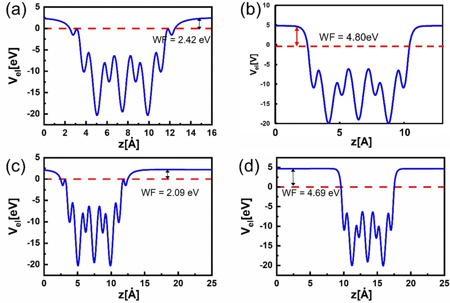 | ||
| Fig. 5 Plane averaged electronic potential vs. z for (a) –OH terminated MXene at HCP sites. (b) –F terminated MXene at FCC sites. (c) N-doped –OH HCP terminated MXene. (d) N-doped FCC –F terminated MXene. Here, nitrogen doping is performed by replacing one of the carbon atoms in the Ti3C2Tx lattice. –OH HCP and –F FCC termination sites were chosen as these configurations are energetically favourable for performing nitrogen doping. | ||
Next, we replaced one of the carbon atoms in the Ti3C2Tx lattice with one nitrogen atom. Notably, by performing nitrogen doping, –OH terminated MXene at HCP sites (Fig. 5(c)) underwent a lowering of WF from 2.42 to 2.09 eV. In the case of –F terminated MXene at FCC sites (Fig. 5(d)), WF lowers from 4.80 to 4.69 eV. Thus, we observed a similar decreasing WF trend for both configurations when introducing a nitrogen atom to the lattice. This finding is quite different when nitrogen atoms terminate the MXene surface, in which WF can reach up to 9 eV. Therefore, we argued that the low WF experimental value of N-MXene (4.30 eV for N-MXene on Au and 4.22 for N-MXene on SiO2) could also be caused by nitrogen atom that occupied the carbon lattice of MXene structure partially by forming Ti–N bond as supported by XPS analysis.
Fig. S20a–d (ESI†) displays the PDOS and DOS of N-MXene, where nitrogen replaces one carbon atom. First, by comparing the electronic states between –OH terminated and –F terminated MXene, it becomes clear that –OH termination gives more electronic states at the Fermi level compared to –F terminated MXene. In particular, –OH terminated MXene shows the majority of Ti 3d states at the Fermi level with a weak contribution of C 2p, O 2p, and H 1s hybridizations (Fig. S20a, ESI†). In the case of –F terminated MXene (Fig. S20b, ESI†), we only observe Ti 3d states at the Fermi level.
After we discussed the electronic structures of F-MXene and N-MXene, we moved to the electronic structure of MAPbI3 grown on Au and SiO2 substrates. The measured SECO region of perovskite samples is presented in Fig. S21 (ESI†). We can see that the secondary electron offset of the spectra gave WF of 4.09 eV and 4.52 eV for MAPbI3 on Au and SiO2, respectively. The differences in these values can be attributed to the different chemical natures of the samples. Previous theoretical studies revealed that the WF of MAPbI3 can be tuned between 4.00 and 4.80 eV for PbI2 rich and MAI rich, respectively.55
Next, we study the MXene WF changes upon the fabrication of MAPbI3/MXene heterostructured thin film. The WF estimated by the SECO is presented in Fig. 6(a). By introducing N-MXene into the targeted hybrid perovskite structure, we see that MAPbI3 exhibited a slightly lower WF, i.e., 4.45 eV and 4.35 eV for N-MXene/MAPbI3 grown on Au and SiO2, respectively. Interestingly, a dramatic lowering of WF is observed when MAPbI3 is combined with F-MXene. MAPbI3/F-MXene grown on Au and SiO2 show WF of 3.00 and 3.45 eV, respectively. Our results suggest that N-MXene and F-MXene act as an n-dopant, which upshifts the Fermi energy of the perovskite towards the vacuum level. In this case, a robust interfacial connection of MXene/perovskite is established, in which electrons are transferred from low-work function MXene to the perovskite layers and induce the interface dipole.2 A similar mechanism has been experimentally observed in N-doped graphene quantum dot/MAPbI3.56 To determine the valence band maximum (VBM) of MXene/MAPbI3 thin film, the UPS valence band region is presented in Fig. 6(b). The VBM of N-MXene/MAPbI3 thin film deposited on Au and SiO2 are 3.50 and 7.62 eV, respectively. Moreover, in F-MXene/MAPbI3, the VBM value is estimated to be 5.12 eV (on Au) and 3.45 eV (on SiO2). Table S5 (ESI†) summarised the WF and VBM changes of MAPbI3/MXene heterostructure on Au and SiO2 substrates.
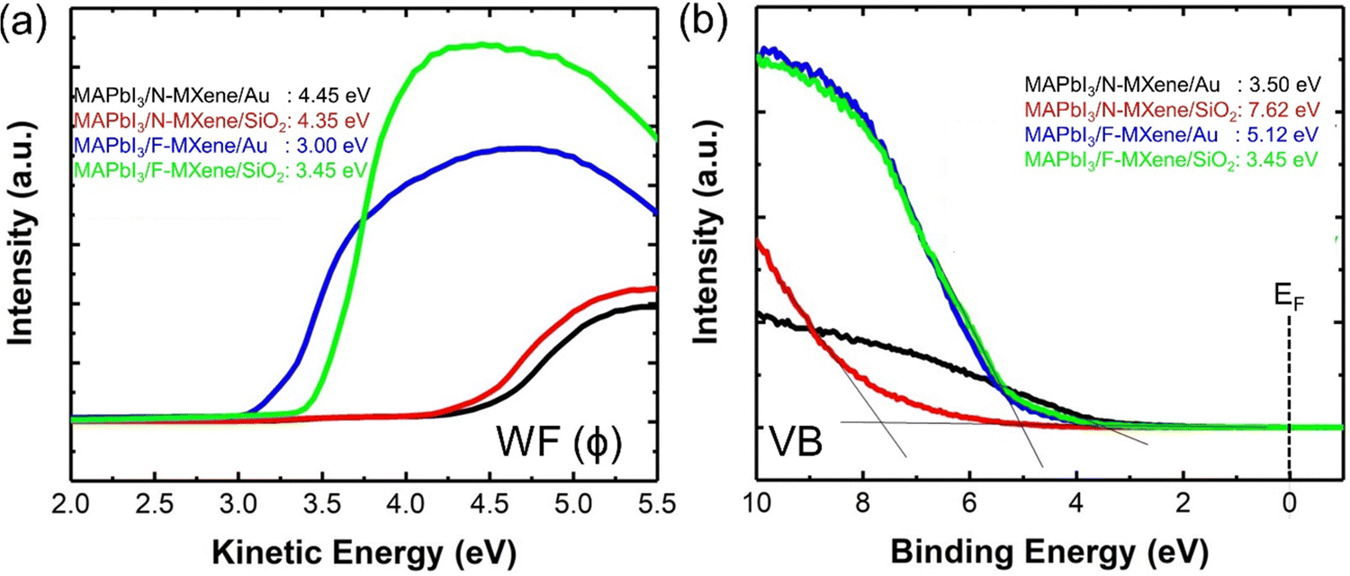 | ||
| Fig. 6 The spectral evolution of MXenes upon MAPbI3 doping. (a) The respective values are shown as indicated in the SECO region and (b) the valence band region where the valence band maximum (VBM) is acquired at the interpolation from the spectral edge to the baseline. | ||
We further investigate the optical properties of F-MXene, N-MXene, and MAPbI3/MXene heterostructured thin film via PL measurements. Fig. 7(a) reveals that F-MXene and N-MXene exhibit relatively weak PL signals with peaks at 450 and 400 nm, respectively.57 From our DOS results, F-MXene and N-MXene are good conductors owing to their rich electronic states at the Fermi level. Thus, the weak observed PL signal does not originate from Ti3C2Tx flakes. The observed PL emission of the samples corresponds to TiO2 species on the surface,57 as we detected TiO2 and TiO2−xFx in both F-MXene and N-MXene in Ti 2p XPS spectra. Furthermore, the slight difference in the PL peak position of N-MXene and F-MXene may be due to different native defects present in the TiO2 lattice.57,58
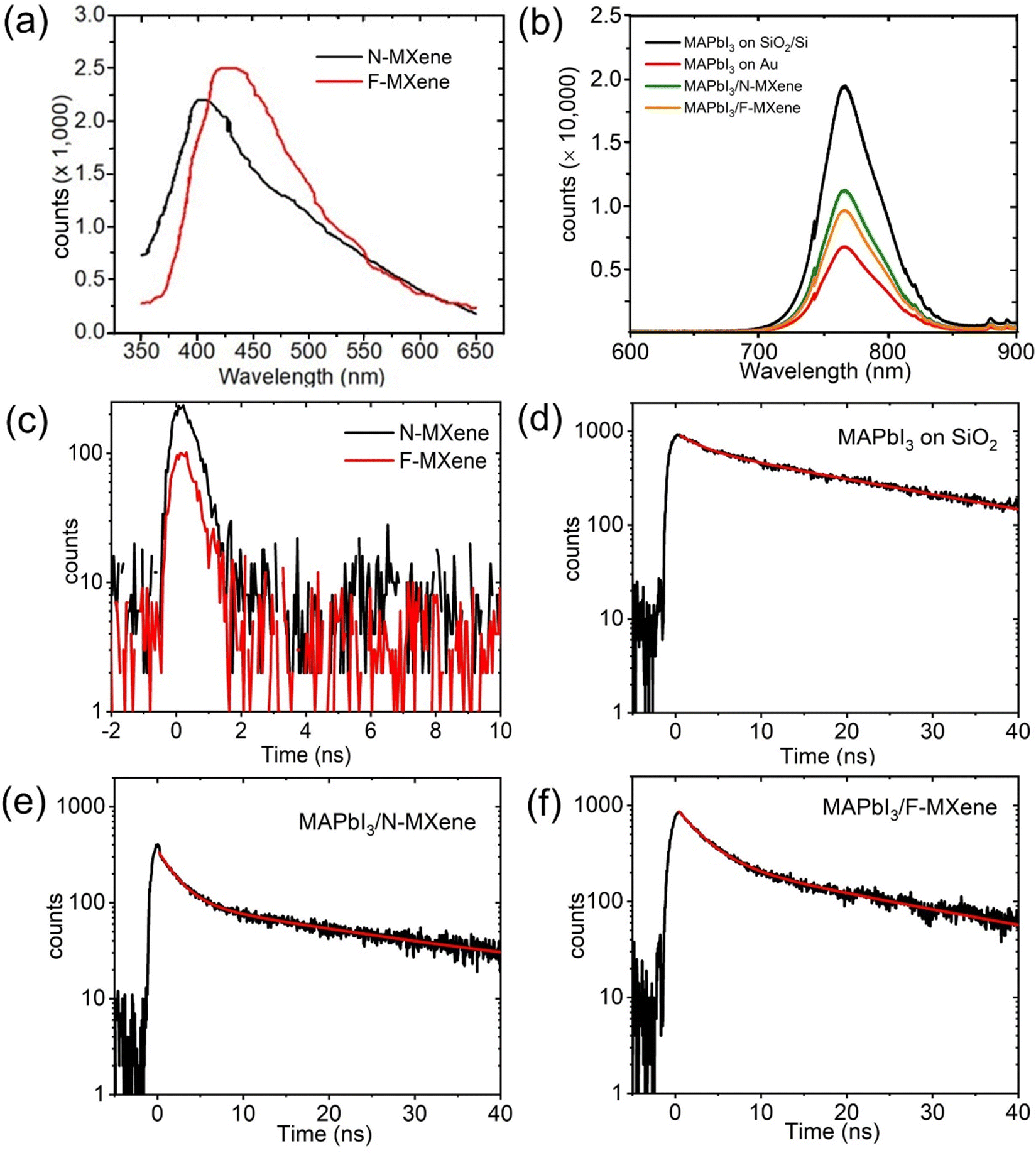 | ||
| Fig. 7 Optical properties of N-MXenes and F-MXenes and their interactions with MAPbI3. (a) Steady-state photoluminescence (PL) spectra of pristine MXenes samples. (b) PL spectra of MAPbI3/MXenes heterostructure. Time-resolved PL (TR-PL) decay curve of (c) N- and F-MXenes, (d) MAPbI3 on SiO2, (e) MAPbI3 on N-MXenes, and (f) MAPbI3 on F-MXenes. (a) and (c) were obtained with excitation at 266 nm, while (b), (d), (e), and (f) were at 532 nm. Decay curve of (b) for 450 nm emission while those of (d), (e), (f) for emission beyond 650 nm. | ||
To further investigate the PL properties of MAPbI3/MXene heterostructure in detail, we also examined the PL response of bare MAPbI3 films. Under 532 nm laser excitation, a strong PL intensity with a broad peak was observed at 766 nm for the corresponding films (Fig. 7(b)), which agrees with the previous reports.59,60 Moreover, we find that the PL intensity of MAPbI3 deposition on Au is lower than on SiO2, possibly due to factors such as non-radiative recombination centres, variation in film thickness, and crystal quality.61,62 Upon the formation of MAPbI3/MXene heterostructure, the PL is strongly quenched, which might be attributed to the n-doping or charge transfer effect between MXene and perovskite at the interface.63,64 Additionally, PL quenching is an indicator of excellent interfacial contact in metal/semiconductor heterostructure.65 We measured TR-PL decay curves to further explore the charge carrier dynamics in MXene thin films (Fig. 7(c)). Both N-MXene and F-MXene exhibited a rapid decay, which might be attributed to the charge transfer from light-active TiO2 to Ti3C2Tx through a Schottky interface. TR-PL spectra of MAPbI3 on SiO2 thin film are presented in Fig. 7(d). The decay curve is fitted by two components (Table 1). The first decay (2.9 ns) is attributed to the emission from the self-trapped excitons, whereas the second decay (26 ns) is related to the emission from the recombination of free carriers.66 The average decay time of MAPbI3 on SiO2 is calculated to be 16.6 ns.
| Sample | τ 1 (ns) | A 1 (%) | τ 2 (ns) | A 2 (%) | τ avg (ns) |
|---|---|---|---|---|---|
| MAPbI3 on SiO2 | 2.9 | 5 | 26.0 | 95 | 16.6 |
| MAPbI3/N-MXene | 2.2 | 23 | 26.4 | 77 | 14.2 |
| MAPbI3/F-MXene | 3.0 | 24 | 23.8 | 76 | 12.5 |
Next, we investigate the decay profile of MAPbI3/MXene heterostructure thin films, which has shown promising potential in tuning the performance of perovskite-based optoelectronic devices. As illustrated in Fig. 7(e), TR-PL spectra of MAPbI3/N-MXene reveal a decreased average decay time of 14.2 ns, compared to pristine MAPbI3, with a decay time of 16.6 ns. Introducing F-MXene in the heterostructure (Fig. 7(f)) further decreased the decay time to an average lifetime of 12.5 ns. This faster carrier lifetime in MAPbI3/F-MXene, as compared to MAPbI3/N-MXene, can be attributed to the more efficient charge transfer pathway provided by F-MXene, resulting in more substantial PL quenching. The different PL quenching is connected to different doped-MXene/perovskite heterostructure interfacial properties. Previously, Tao et al. demonstrated that the charge transfer ability of Ti3C2Tx can be controlled by introducing different types of surface functional groups.67 They constructed WS2/Ti3C2Tx heterostructure and showed that F-MXene has more efficient charge transfer than N-MXene. Thus, our findings demonstrate the potential of F-MXene to tune the electronic structure of perovskite-based optoelectronic devices effectively.
4. Conclusion
This study presents a comprehensive interfacial engineering of the optoelectronic properties of Ti3C2Tx MXene/MAPbI3 heterostructures by tuning the WF of MAPbI3. We elucidated the chemical states of Ti3C2Tx of respective fluorine termination (F-MXene) and nitrogen doping (N-MXene) by the XPS technique. Fluorine atoms decorated the outermost surface of F-MXene, while nitrogen atoms were partially adsorbed on the N-MXene surface and doped the crystal lattice.The UPS spectra have shown that the F-termination and N-doping of Ti3C2Tx yield low WFs ranging from 3.34 to 4.30 eV. These experimental results are comparable with DFT results, considering four adsorption sites of the respective atoms (hexagonal closed-packed, face-centred cubic, bridge, and top sites). MXene/MAPbI3 heterostructures constructed from F-terminated and N-doped MXenes further result in WF tuning of MAPbI3 within 3.00–4.45 eV. Due to the efficient charge transfer pathway, strong PL quenching and faster average decay time were observed for both heterostructures compared to pristine counterparts.
Altogether, our results show excellent MXene/MAPbI3 heterostructure tunability regarding WF and optical properties by surface termination and non-metal elemental doping. The obtained results formulate an essential step for tailoring the interfacial electronic structure of MXenes toward optoelectronic applications.
Author contributions
MAKP: investigation, formal analysis, data curation, visualization, and writing – original draft. A: conceptualization, methodology, data curation, resources, supervision, and writing – review & editing. SWK: investigation and validation. FM: investigation and validation. DM: investigation. JM: investigation, formal analysis, visualization, and writing – review & editing. YD: investigation, resources, and writing – review & editing. DK: investigation and writing – review & editing. HL: resources and supervision. MDB: resources, project administration, conceptualization, writing – review & editing, and supervision. AMJ: supervision and writing – review & editing.Conflicts of interest
There are no conflicts of interest to declare.Acknowledgements
M. A. K. P. acknowledges the Preludium-21 grant (UMO-2022/45/N/ST5/02472). F. M. and M. D. B acknowledge financial support from the Singapore Ministry of Education (T2EP50121-0025) and the OPUS-24 grant (2022/47/B/ST5/01966), respectively. A. acknowledges the MOE Tier 2 grant (MOE2018-T2-1-088). J. M. and Y. D. acknowledge the PMDSU scholarship and 2023 research program from the Ministry of Education, Culture, Research and Technology of the Republic of Indonesia, respectively.References
- M. L. Agiorgousis, Y.-Y. Sun, H. Zeng and S. Zhang, Strong Covalency-Induced Recombination Centers in Perovskite Solar Cell Material CH3NH3PbI3, J. Am. Chem. Soc., 2014, 136, 14570–14575 CrossRef CAS PubMed.
- A. Di Vito, A. Pecchia, M. Auf der Maur and A. Di Carlo, Nonlinear work function tuning of lead-halide perovskites by MXenes with mixed terminations, Adv. Funct. Mater., 2020, 30, 1909028 CrossRef CAS.
- M. Naguib, M. Kurtoglu, V. Presser, J. Lu, J. Niu, M. Heon, L. Hultman, Y. Gogotsi and M. W. Barsoum, Two-dimensional nanocrystals produced by exfoliation of Ti3AlC2, Adv. Mater., 2011, 23, 4248–4253 CrossRef CAS PubMed.
- S. Abdolhosseinzadeh, X. Jiang, H. Zhang, J. Qiu and C. J. Zhang, Perspectives on solution processing of two-dimensional MXenes, Mater. Today, 2021, 48, 214–240 CrossRef CAS.
- A. S. Zeraati, S. A. Mirkhani, P. Sun, M. Naguib, P. V. Braun and U. Sundararaj, Improved synthesis of Ti3C2Tx MXenes resulting in exceptional electrical conductivity, high synthesis yield, and enhanced capacitance, Nanoscale, 2021, 13, 3572–3580 RSC.
- A. D. Dillon, M. J. Ghidiu, A. L. Krick, J. Griggs, S. J. May, Y. Gogotsi, M. W. Barsoum and A. T. Fafarman, Highly conductive optical quality solution-processed films of 2D titanium carbide, Adv. Funct. Mater., 2016, 26, 4162–4168 CrossRef CAS.
- M. Khazaei, M. Arai, T. Sasaki, C. Chung, N. S. Venkataramanan, M. Estili, Y. Sakka and Y. Kawazoe, Novel electronic and magnetic properties of two-dimensional transition metal carbides and nitrides, Adv. Funct. Mater., 2013, 23, 2185–2192 CrossRef CAS.
- T. Schultz, N. C. Frey, K. Hantanasirisakul, S. Park, S. J. May, V. B. Shenoy, Y. Gogotsi and N. Koch, Surface termination dependent work function and electronic properties of Ti3C2Tx MXene, Chem. Mater., 2019, 31, 6590–6597 CrossRef CAS.
- H. Jing, H. Yeo, B. Lyu, J. Ryou, S. Choi, J.-H. Park, B. H. Lee, Y.-H. Kim and S. Lee, Modulation of the electronic properties of MXene (Ti3C2Tx) via surface-covalent functionalization with diazonium, ACS Nano, 2021, 15, 1388–1396 CrossRef CAS PubMed.
- Y. Liu, H. Xiao and W. A. Goddard III, Schottky-barrier-free contacts with two-dimensional semiconductors by surface-engineered MXenes, J. Am. Chem. Soc., 2016, 138, 15853–15856 CrossRef CAS PubMed.
- M. Khazaei, M. Arai, T. Sasaki, A. Ranjbar, Y. Liang and S. Yunoki, OH-terminated two-dimensional transition metal carbides and nitrides as ultralow work function materials, Phys. Rev. B: Condens. Matter Mater. Phys., 2015, 92, 075411 CrossRef.
- A. Agresti, A. Pazniak, S. Pescetelli, A. Di Vito, D. Rossi, A. Pecchia, M. Auf der Maur, A. Liedl, R. Larciprete and D. V. Kuznetsov, Titanium-carbide MXenes for work function and interface engineering in perovskite solar cells, Nat. Mater., 2019, 18, 1228–1234 CrossRef CAS PubMed.
- Z. Zhong and P. Hansmann, Tuning the work function in transition metal oxides and their heterostructures, Phys. Rev. B, 2016, 93, 235116 CrossRef.
- A. M. Al-Amri, B. Cheng and J.-H. He, Perovskite methylammonium lead trihalide heterostructures: progress and challenges, IEEE Trans. Nanotechnol., 2018, 18, 1–12 Search PubMed.
- Y. Bao, Y. Liu, J. Pan, P. Chen, X. Liu, Y. Li, X. Tang, W. Zhang, B. Liu and J. Liu, Constructing 2D layered PCN/Ti3C2/Bi2MoO6 heterojunction with MXene as charge mediator for enhanced photocatalytic performance, Appl. Surf. Sci., 2022, 589, 152883 CrossRef CAS.
- J. Zhu, H. Wang, L. Ma and G. Zou, Observation of ambipolar photoresponse from 2D MoS2/MXene heterostructure, Nano Res., 2021, 14, 3416–3422 CrossRef CAS.
- M. A. K. Purbayanto, M. Chandel, M. Birowska, A. Rosenkranz and A. M. Jastrzębska, Optically Active MXenes in van der Waals Heterostructures, Adv. Mater., 2023, 2301850 CrossRef CAS PubMed.
- M. A. K. Purbayanto, D. Bury, M. Chandel, Z. D. Shahrak, V. N. Mochalin, A. Wójcik, D. Moszczyńska, A. Wojciechowska, A. Tabassum, M. Naguib and A. M. Jastrzębska, Ambient Processed rGO/Ti3CNTx MXene Thin Film with High Oxidation Stability, Photosensitivity, and Self-Cleaning Potential, ACS Appl. Mater. Interfaces, 2023, 15, 44075–44086 CrossRef CAS PubMed.
- A. S. Bati, A. A. Sutanto, M. Hao, M. Batmunkh, Y. Yamauchi, L. Wang, Y. Wang, M. K. Nazeeruddin and J. G. Shapter, Cesium-doped Ti3C2Tx MXene for efficient and thermally stable perovskite solar cells, Cell Rep. Phys. Sci., 2021, 2, 100598 CrossRef CAS.
- Z. Guo, L. Gao, Z. Xu, S. Teo, C. Zhang, Y. Kamata, S. Hayase and T. Ma, High electrical conductivity 2D MXene serves as additive of perovskite for efficient solar cells, Small, 2018, 14, 1802738 CrossRef PubMed.
- Z. Guo, J. Zhou and Z. Sun, New two-dimensional transition metal borides for Li ion batteries and electrocatalysis, J. Mater. Chem. A, 2017, 5, 23530–23535 RSC.
- S. Wei, S. Tie, K. Shen, H. Sun, X. Zheng, H. Wang, W. Liang, J. Zou, Y. Huang and L. Luo, Enhanced Carrier Transport in X-Ray Detector Based on Cs3Bi2I9/MXene Composite Wafers, Adv. Opt. Mater., 2022, 10, 2201585 CrossRef CAS.
- C. Lu, L. Yang, B. Yan, L. Sun, P. Zhang, W. Zhang and Z. Sun, Nitrogen-doped Ti3C2 MXene: mechanism investigation and electrochemical analysis, Adv. Funct. Mater., 2020, 30, 2000852 CrossRef CAS.
- R. Wang, M. Li, K. Sun, Y. Zhang, J. Li and W. Bao, Element-Doped Mxenes: Mechanism, Synthesis, and Applications, Small, 2022, 18, 2201740 CrossRef CAS PubMed.
- Y. Wen, T. E. Rufford, X. Chen, N. Li, M. Lyu, L. Dai and L. Wang, Nitrogen-doped Ti3C2Tx MXene electrodes for high-performance supercapacitors, Nano Energy, 2017, 38, 368–376 CrossRef CAS.
- L. Pu, J. Zhang, N. K. L. Jiresse, Y. Gao, H. Zhou, N. Naik, P. Gao and Z. Guo, N-doped MXene derived from chitosan for the highly effective electrochemical properties as supercapacitor, Adv. Compos. Hybrid Mater., 2022, 1–14 Search PubMed.
- W. Xu, S. Li, W. Zhang, B. Ouyang, W. Yu and Y. Zhou, Nitrogen-Doped Ti3C2Tx MXene Induced by Plasma Treatment with Enhanced Microwave Absorption Properties, ACS Appl. Mater. Interfaces, 2021, 13, 49242–49253 CrossRef CAS PubMed.
- L. Tjahjana, A. Olivier, Y. Herbani, H. Hardhienata, F. Ahmad, Arramel, D. Kowal, M. D. Birowosuto and H. Wang, Localized Visible Wavelength Photoluminescence from GaP/InP Heterostructure Nanowires, J. Phys. Chem. C, 2022, 126, 12113–12120 CrossRef CAS.
- P. Giannozzi, S. Baroni, N. Bonini, M. Calandra, R. Car, C. Cavazzoni, D. Ceresoli, G. L. Chiarotti, M. Cococcioni and I. Dabo, QUANTUM ESPRESSO: a modular and open-source software project for quantum simulations of materials, J. Phys.: Condens. Matter, 2009, 21, 395502 CrossRef PubMed.
- J. P. Perdew and A. Zunger, Self-interaction correction to density-functional approximations for many-electron systems, Phys. Rev. B: Condens. Matter Mater. Phys., 1981, 23, 5048 CrossRef CAS.
- Y. Li, H. Shao, Z. Lin, J. Lu, L. Liu, B. Duployer, P. O. Persson, P. Eklund, L. Hultman and M. Li, A general Lewis acidic etching route for preparing MXenes with enhanced electrochemical performance in non-aqueous electrolyte, Nat. Mater., 2020, 19, 894–899 CrossRef CAS PubMed.
- M. Naguib, V. N. Mochalin, M. W. Barsoum and Y. Gogotsi, 25th anniversary article: MXenes: a new family of two-dimensional materials, Adv. Mater., 2014, 26, 992–1005 CrossRef CAS PubMed.
- K. Liang, A. Tabassum, A. Majed, C. Dun, F. Yang, J. Guo, K. Prenger, J. J. Urban and M. Naguib, Synthesis of new two-dimensional titanium carbonitride Ti2C0.5N0.5Tx MXene and its performance as an electrode material for sodium-ion battery, InfoMat, 2021, 3, 1422–1430 CrossRef CAS.
- E. B. Deeva, A. Kurlov, P. M. Abdala, D. Lebedev, S. M. Kim, C. P. Gordon, A. Tsoukalou, A. Fedorov and C. R. Müller, In Situ XANES/XRD Study of the Structural Stability of Two-Dimensional Molybdenum Carbide Mo2CTx: Implications for the Catalytic Activity in the Water–Gas Shift Reaction, Chem. Mater., 2019, 31, 4505–4513 CrossRef CAS.
- J. Halim, K. M. Cook, M. Naguib, P. Eklund, Y. Gogotsi, J. Rosen and M. W. Barsoum, X-ray photoelectron spectroscopy of select multi-layered transition metal carbides (MXenes), Appl. Surf. Sci., 2016, 362, 406–417 CrossRef CAS.
- J. D. Gouveia and J. R. B. Gomes, The determining role of Tx species in the catalytic potential of MXenes: Water adsorption and dissociation on Mo2CTx, Catal. Today, 2023, 424, 113848 CrossRef CAS.
- V. Natu, M. Benchakar, C. Canaff, A. Habrioux, S. Celerier and M. W. Barsoum, A critical analysis of the X-ray photoelectron spectra of Ti3C2Tz MXenes, Matter, 2021, 4, 1224–1251 CrossRef CAS.
- L. Yu, Z. Fan, Y. Shao, Z. Tian, J. Sun and Z. Liu, Versatile N-doped MXene ink for printed electrochemical energy storage application, Adv. Energy Mater., 2019, 9, 1901839 CrossRef.
- Y. Tang, J. Zhu, W. Wu, C. Yang, W. Lv and F. Wang, Synthesis of nitrogen-doped two-dimensional Ti3C2 with enhanced electrochemical performance, J. Electrochem. Soc., 2017, 164, A923 CrossRef CAS.
- S.-Y. Liao, S.-F. Cui, Y.-Z. Li, W.-X. Cheng, X.-W. Huang, J. Zhang, T.-T. Cui, X.-G. Shu and Y.-G. Min, Wrinkled and flexible N-doped MXene additive for improving the mechanical and electrochemical properties of the nickel-rich LiNi0.8Co0.1Mn0.1O2 cathode, Electrochim. Acta, 2022, 410, 139989 CrossRef CAS.
- C. Rocks, V. Svrcek, P. Maguire and D. Mariotti, Understanding surface chemistry during MAPbI3 spray deposition and its effect on photovoltaic performance, J. Mater. Chem. C, 2017, 5, 902–916 RSC.
- H. Xie, X. Liu, L. Lyu, D. Niu, Q. Wang, J. Huang and Y. Gao, Effects of precursor ratios and annealing on electronic structure and surface composition of CH3NH3PbI3 perovskite films, J. Phys. Chem. C, 2016, 120, 215–220 CrossRef CAS.
- Z. Shao, S. You, X. Guo, J. Xiao, J. Liu, F. Song, H. Xie, J. Sun and H. Huang, Temperature-dependent photoluminescence of Co-evaporated MAPbI3 ultrathin films, Results Phys., 2022, 34, 105326 CrossRef.
- S. Olthof and K. Meerholz, Substrate-dependent electronic structure and film formation of MAPbI3 perovskites, Sci. Rep., 2017, 7, 40267 CrossRef CAS PubMed.
- F. Amy, C. Chan and A. Kahn, Polarization at the gold/pentacene interface, Org. Electron., 2005, 6, 85–91 CrossRef CAS.
- F. Zhang, S. H. Silver, N. K. Noel, F. Ullrich, B. P. Rand and A. Kahn, Ultraviolet photoemission spectroscopy and Kelvin probe measurements on metal halide perovskites: Advantages and pitfalls, Adv. Energy Mater., 2020, 10, 1903252 CrossRef CAS.
- M. Tamulewicz, J. Kutrowska-Girzycka, K. Gajewski, J. Serafińczuk, A. Sierakowski, J. Jadczak, L. Bryja and T. P. Gotszalk, Layer number dependence of the work function and optical properties of single and few layers MoS2: effect of substrate, Nanotechnology, 2019, 30, 245708 CrossRef CAS PubMed.
- Y. Liu, Y.-H. Li, X. Li, Q. Zhang, H. Yu, X. Peng and F. Peng, Regulating Electron–Hole Separation to Promote Photocatalytic H2 Evolution Activity of Nanoconfined Ru/MXene/TiO2 Catalysts, ACS Nano, 2020, 14, 14181–14189 CrossRef CAS PubMed.
- P. Zhang, Y. Li, Y. Zhang, R. Hou, X. Zhang, C. Xue, S. Wang, B. Zhu, N. Li and G. Shao, Photogenerated Electron Transfer Process in Heterojunctions: In Situ Irradiation XPS, Small Methods, 2020, 4, 2000214 CrossRef CAS.
- G. Ding, K. Zeng, K. Zhou, Z. Li, Y. Zhou, Y. Zhai, L. Zhou, X. Chen and S.-T. Han, Configurable multi-state non-volatile memory behaviors in Ti3C2 nanosheets, Nanoscale, 2019, 11, 7102–7110 RSC.
- P. P. Michałowski, M. Anayee, T. S. Mathis, S. Kozdra, A. Wójcik, K. Hantanasirisakul, I. Jóźwik, A. Piątkowska, M. Możdżonek, A. Malinowska, R. Diduszko, E. Wierzbicka and Y. Gogotsi, Oxycarbide MXenes and MAX phases identification using monoatomic layer-by-layer analysis with ultralow-energy secondary-ion mass spectrometry, Nat. Nanotechnol., 2022, 17, 1192–1197 CrossRef PubMed.
- G. M. Song, S. B. Li, C. X. Zhao, W. G. Sloof, S. van der Zwaag, Y. T. Pei and J. Th. M. De Hosson, Ultra-high temperature ablation behavior of Ti2AlC ceramics under an oxyacetylene flame, J. Eur. Ceram, 2011, 31, 855–862 CrossRef CAS.
- X. H. Wang and Y. C. Zhou, Stability and Selective Oxidation of Aluminum in Nano-Laminate Ti3AlC2 upon Heating in Argon, Chem. Mater., 2003, 15, 3716–3720 CrossRef CAS.
- J. Manopo, P. N. Kusumo, A. Sumboja and Y. Darma, Coordination engineering of atomically dispersed zirconium on graphene for the oxygen reduction reaction, Phys. Chem. Chem. Phys., 2023, 25, 25299–25308 RSC.
- W.-J. Yin, T. Shi and Y. Yan, Unusual defect physics in CH3NH3PbI3 perovskite solar cell absorber, Appl. Phys. Lett., 2014, 104, 063903 CrossRef.
- X. Gan, S. Yang, J. Zhang, G. Wang, P. He, H. Sun, H. Yuan, L. Yu, G. Ding and Y. Zhu, Graphite-N doped graphene quantum dots as semiconductor additive in perovskite solar cells, ACS Appl. Mater. Interfaces, 2019, 11, 37796–37803 CrossRef CAS PubMed.
- L. Zhang, W. Su, H. Shu, T. Lü, L. Fu, K. Song, X. Huang, J. Yu, C.-T. Lin and Y. Tang, Tuning the photoluminescence of large Ti3C2Tx MXene flakes, Ceram. Int., 2019, 45, 11468–11474 CrossRef CAS.
- X. Sang, Y. Xie, M.-W. Lin, M. Alhabeb, K. L. Van Aken, Y. Gogotsi, P. R. C. Kent, K. Xiao and R. R. Unocic, Atomic Defects in Monolayer Titanium Carbide (Ti3C2Tx) MXene, ACS Nano, 2016, 10, 9193–9200 CrossRef CAS PubMed.
- Q. Zhu, X. Bao, J. Yu, D. Zhu, M. Qiu, R. Yang and L. Dong, Compact layer free perovskite solar cells with a high-mobility hole-transporting layer, ACS Appl. Mater. Interfaces, 2016, 8, 2652–2657 CrossRef CAS PubMed.
- A. F. Akbulatov, L. A. Frolova, S. A. Tsarev, I. Zhidkov, S. Y. Luchkin, E. Z. Kurmaev, K. J. Stevenson, S. M. Aldoshin and P. A. Troshin, Film deposition techniques impact the defect density and photostability of MAPbI3 Perovskite films, J. Phys. Chem. C, 2020, 124, 21378–21385 CrossRef CAS.
- S. Parveen, S. M. Obaidulla and P. Giri, Growth kinetics of hybrid perovskite thin films on different substrates at elevated temperature and its direct correlation with the microstructure and optical properties, Appl. Surf. Sci., 2020, 530, 147224 CrossRef CAS.
- Y. Xue, J. Yuan, J. Liu and S. Li, Controllable synthesis of 2D perovskite on different substrates and its application as photodetector, Nanomaterials, 2018, 8, 591 CrossRef PubMed.
- W. Li, F. Wang, Z. Zhang and S. Min, MAPbI3 microcrystals integrated with Ti3C2Tx MXene nanosheets for efficient visible-light photocatalytic H2 evolution, Chem. Commun., 2021, 57, 7774–7777 RSC.
- J. M. Bharathan and Y. Yang, Polymer/metal interfaces and the performance of polymer light-emitting diodes, J. Appl. Phys., 1998, 84, 3207–3211 CrossRef CAS.
- H. Tan, Y. Fan, Y. Rong, B. Porter, C. S. Lau, Y. Zhou, Z. He, S. Wang, H. Bhaskaran and J. H. Warner, Doping graphene transistors using vertical stacked monolayer WS2 heterostructures grown by chemical vapor deposition, ACS Appl. Mater. Interfaces, 2016, 8, 1644–1652 CrossRef CAS PubMed.
- K. J. Karki, M. Abdellah, W. Zhang and T. Pullerits, Different emissive states in the bulk and at the surface of methylammonium lead bromide perovskite revealed by two-photon micro-spectroscopy and lifetime measurements, APL Photonics, 2016, 1, 046103 CrossRef.
- Y. Tao, S. W. Koh, X. Yu, C. Wang, H. Liang, Y. Zhang, H. Li and Q. J. Wang, Surface group-modified MXene nano-flake doping of monolayer tungsten disulfides, Nanoscale Adv., 2019, 1, 4783–4789 RSC.
Footnote |
| † Electronic supplementary information (ESI) available: Figures: SEM images of F-MXene and N-MXene; EDS of F-MXene; XPS survey spectra of N-MXene and F-MXene; XPS spectra of F-MXene, N-MXene, and the MAPbI3/MXene heterostructure; EDS mapping of the F-MXene/MAPbI3 heterostructure; plane averaged electrostatic potential vs. z for F-MXene, N-MXene, and –OH terminated MXene; PDOS and DOS of –OH terminated MXene, F-terminated MXene, and N-doped MXene; ELF of F-MXene FCC and N-MXene HCP; SECO signals of MAPbI3. Tables: chemical composition of as-synthesized MXene obtained from EDS; relative formation energy for every adsorption site of F- and N-MXene; summary of MXene WF obtained from experiment and DFT prediction; and summary of WF and VB changes in MXene/MAPbI3 heterostructures. See DOI: https://doi.org/10.1039/d3cp04018f |
| This journal is © the Owner Societies 2023 |