
 Open Access Article
 This Open Access Article is licensed under a
 Creative Commons Attribution 3.0 Unported Licence
Hematite photoanodes for water splitting from directed assembly of Prussian blue onto CuO–Sb2O5–SnO2 ceramics
Alexander N.
Bondarchuk
 *ab and
Frank
Marken
b
*ab and
Frank
Marken
b
aUniversidad Tecnológica de la Mixteca, Huajuapan 69000, Oaxaca, Mexico. E-mail: alexbondua@yahoo.com
bDepartment of Chemistry, University of Bath, Claverton Down, Bath BA2 7AY, UK
First published on 31st August 2023
Abstract
We report the controlled layer-by-layer growth by the directed assembly of Prussian blue to form (via thermolysis) a functional hematite coating on the grain surfaces of porous CuO–Sb2O5–SnO2 ceramics. The impact of the hematite coating on the physicochemical properties of the ceramics is demonstrated through Raman spectroscopy, and photoelectric and electrochemical impedance measurements. The directed assembly of ionic layers described here is a promising approach for introducing thin film deposits into porous structures and modifying/tuning the photoelectrochemical properties of SnO2-based ceramic materials.
1. Introduction
Developing modern sensors, photoelectrodes, and other functional components requires the ability to engineer the physical and chemical properties of material surfaces using simple and cost-effective chemical methods. Surface modification of sensor materials using specific coatings can significantly improve their sensitivity and selectivity to analytes, enabling detection with improved accuracy and reliability.1–7 This type of surface modification is particularly important for oxide ceramics, which are widely used as photoanodes or sensors to detect gases, pressure, humidity, and temperature.8–15 In the design of photoelectrodes, a functional coating or a co-catalyst layer on the surface can increase their ability to absorb light or enhance the kinetics of surface reactions, resulting in improved efficiency in converting light into electrical energy.16–25One of the promising low-cost methods to create a functional coating on the surface of host materials is a ‘directed assembly’ of charged multi-layers on a host surface.26 This approach was proposed26 to grow redox-active multilayers of Prussian blue (PB) and Ruthenium purple on the surfaces of materials. In a proof-of-concept experiment,26 a gold electrode was alternately immersed into solutions with the positively charged ferric cations (Fe3+) and negatively charged ferrocyanide Fe(CN)64− anions, which reacted and formed a layer-by-layer of the coordination polymer, Prussian blue. The repetition of this procedure resulted in a multilayer coating on the host surface. Thus, the thickness of the Prussian blue coating can be controlled by the experimenter with monolayer precision.26 This favourably distinguishes the directed assembly method from self-assembly27–32 or other spontaneous processes of deposition.33–38
In the present work, we apply the directed assembly method to grow a functional layer of Prussian blue (which is then converted thermally to hematite) with nanometre thickness control on the grain surfaces in porous electrically conducting CuO–Sb2O5–SnO2 ceramics. It is shown that the thickness of this coating determines the photocurrent in the obtained photoanode structure. The aim of this work is to test the application of the direct assembly method for the controlled molecular-level engineering of grain surfaces in oxide ceramics, with the goal of producing useful coatings for sensory and photocatalyst applications. Specifically, this approach can be used to modify the photoactive surface of hematite photoelectrodes grown on SnO2-based ceramics.39,40 Such hematite photoelectrodes, grown using the metal–organic chemical vapor deposition (MO-CVD) technique on a free-standing substrate made from CuO–Sb2O5–SnO2 ceramics, exhibit relatively high photocurrent (0.56 mA cm−2 at 1.23 V vs. RHE under AM1.5G radiation), making them promising candidates for further development.39
In this study, we demonstrate the feasibility of creating a functional nanometric coating (Fe2O3 photocatalytic layer) on CuO–Sb2O5–SnO2 ceramics using the direct assembly method. The reported structures and materials are discussed based on the data from photoelectrochemical and electrochemical impedance measurements, Raman spectroscopy, X-ray diffraction (XRD), scanning electron microscopy (SEM), and energy-dispersive X-ray spectroscopy (EDX). Routes to improve the performance of sensor materials are considered.
2. Experimental
Electrically conducting CuO–Sb2O5–SnO2 ceramics were obtained by sintering a mixture of CuO (0.2 mol%), Sb2O5 (1 mol%), and SnO2 (98.8 mol%) at 1300 °C in air, as previously described.39,40 All oxides were purchased from Sigma-Aldrich and had a purity of not less than 99.5%. The CuO–Sb2O5–SnO2 substrates prepared here were in the shape of circular discs with a diameter of 12 mm and about 2 mm thickness. Before Prussian blue deposition, the ceramic substrates were cleaned under a flow of nitrogen gas, then placed on the glass plate covered with paraffin film (Bemis, “M”, Fisher Scientific UK Ltd), and heated to 185 °C for 5 min on a hotplate (Fig. 1(a)). The melted paraffin sealed one side of the ceramic substrate reserving it for the Ag-contact needed later for external connections. Next, the ceramic substrate was alternately immersed for 60 s in a solution of (a) 40 mM K4Fe(CN)6 in 0.1 M HNO3 with negatively charged ions of Fe(CN)64−, (b) then in deionized water to rinse, (c) in 40 mM of Fe2(SO4)3 in 0.1 M HNO3 with positively charged ions of Fe3+, and finally (d) in deionized water. As a result of this treatment cycle, the coordination polymer Prussian blue was formed layer-by-layer on the ceramic surface. The repetition of this procedure resulted in the growth of additional Prussian blue layers. The characteristic blue colour of Prussian blue clearly emerged after five treatment cycles and is seen as a dark blue colour after 26 cycles (Fig. 1(c) and (d)). The samples with Prussian blue coatings were annealed in air at 600 °C for one hour to form a hematite film (Fig. 1(e)). During annealing at 600 °C, the backside of the ceramic substrate reserved for Ag-contact was cleaned with paraffin. The Ag-contact on the ceramic substrate was formed with a quick-drying paste (SPI Supplies, 05002-AB) and soldered to an insulated wire for external connections. Afterwards, the substrate area with Ag-contact was sealed again with hot paraffin (Bemis, “M”). | ||
| Fig. 1 (a) Schematic representation of the prepared sample; (b) bare ceramic substrate; (c) the sample with Prussian blue coating (26 treatment cycles) in the top view, and (d) in the cross-sectional view after being broken; (e) sample with hematite coating (26 cycles of Prussian blue deposition) formed after annealing at 600 °C. | ||
Electrochemical measurements were performed using a microAutolab III potentiostat in a three-electrode configuration: the sample was the working electrode, a Pt-wire served as the counter electrode, and a KCl-saturated calomel (SCE) electrode was the reference one. The electrochemical impedance spectroscopy (EIS) data were obtained using a ModuLab XM PhotoEchem unit. The measurements were conducted over a frequency range of 0.01 Hz to 100 kHz, with an AC signal amplitude of 20 mV and an applied DC voltage of 1.23 V vs. RHE. The fitting of the experimental data was performed using Zview 4 software in the frequency range from 0.01 Hz to 10 kHz.
The electrolyte solution of 1 M NaOH in demineralized water (pH = 13.65) was employed. Potentials versus reversible hydrogen electrodes (RHEs) were calculated using the Nernst equation, ERHE = ESCE + 0.0591 × pH + 0.2415 V, where ESCE is the experimentally measured potential against the SCE. The incident photon-to-current efficiency (IPCE) was estimated using the equation IPCE(λ) = |Jph(mA cm−2)| × 1239.8(V nm)/[P(mW cm−2) × λ (nm)], where Jph is the photocurrent density in the photoelectrode under light with intensity P and wavelength λ. The light sources used were an LED (Thorlabs M365LP1; 365 nm) and the solar simulator was PICO G2V (AM1.5G; 350–1100 nm), providing light intensities of 248 mW cm−2 and 86.6 mW cm−2, respectively.
X-ray diffraction (XRD) patterns were recorded using a RIGAKU Oxford Diffraction SuperNova equipment. Scanning electron microscopy (SEM) images and elemental mapping were obtained with a field emission scanning electron microscope (JEOL JSM-7900F) with an UltiMax energy dispersive X-ray (EDX) detector. Raman spectroscopy was performed with a Renishaw inVia Raman Microscope using 532 nm laser radiation with a power of 2 mW.
3. Results and discussion
Raman spectroscopy data for a bare CuO–Sb2O5–SnO2 substrate and the one with a red Fe2O3-coating formed after annealing at 600 °C (1 h) are presented in Fig. 2. The signal for the bare substrate shows the Raman shifts at approximately 117.5, 238.5, and 624.9 cm−1 (Fig. 2, curve 1), which are attributed to SnO2.41–44 The registered Raman shifts at 238.5 and 624.9 cm−1, along with a broad shoulder-type band at approximately 440–470 cm−1, are indicative of oxygen vacancies in tin oxide.41,42 In turn, the signal obtained for the sample with a red coating (Fig. 1(e)) contains the peaks with maxima at 224.3, 245.9, 292.3, 410.9, 499.3, 612.7, and 1317.1 cm−1 (Fig. 2, curve 2), which are typical for hematite.45 The broad bands observed at approximately 800–836 cm−1 and 1030–1130 cm−1 are attributed to adsorbed oxygen.46 The peak near 659 cm−1 is likely caused by defect-induced scattering in the solid solutions and corresponds to the Raman-forbidden longitudinal optical Eu mode of hematite, as previously reported.47–49 Thus, the obtained Raman data confirms the presence of hematite on the substrate surface after annealing the sample coated with Prussian blue in air at 600 °C for 1 hour. | ||
| Fig. 2 Raman spectra recorded on the surface of the bare CuO–Sb2O5–SnO2 substrate (curve 1) and the one with hematite coating (curve 2). | ||
The XRD patterns recorded for the sample with a red hematite coating (Fig. 1(e)) are presented in Fig. 3. They clearly show the presence of only the tetragonal SnO2 phase (00-077-0447), while the hematite signal is very weak (see the zoomed-in area in Fig. 3). The Cu and Sb-phases remain unobserved, most likely due to their low concentrations being below the detection limit of the diffractometer.
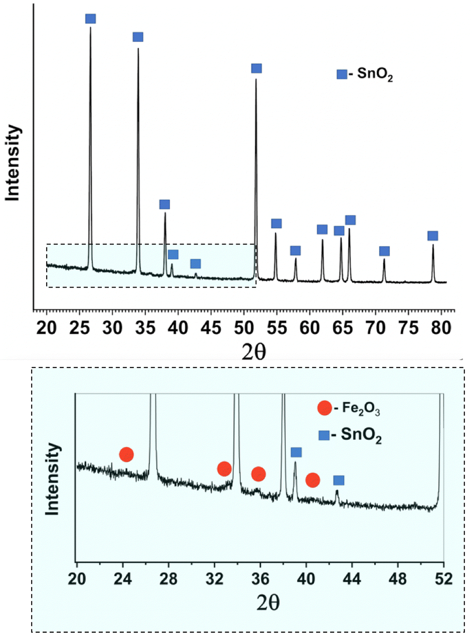 | ||
| Fig. 3 XRD patterns of the CuO–Sb2O5–SnO2 ceramic substrate with hematite coating. The zoomed-in area is highlighted in colour. The blue labels indicate the SnO2 signals, while the red labels—the expected Fe2O3 signals. | ||
SEM micrographs of the bare ceramic substrates and those covered with a Prussian blue coating or hematite are presented in Fig. 4. All obtained structures have high porosity. There is no significant difference in particle size/porosity when comparing the bare ceramics and the coated ceramics. In bare ceramics, the majority of grains have sizes from 300 to 800 nm (Fig. 4(a)). However, some grains with sizes in some micrometres are also found in CuO–Sb2O5–SnO2 ceramics (Fig. 4(f)). As previously reported,39 the bare CuO–Sb2O5–SnO2 ceramics have an average pore size of about 13.9 nm, a surface area of 1.343 m2 g−1, a density of about 6.27 g cm−3 and have an electrical conductivity of 120 S m−1. The surfaces of the ceramic grains in bare ceramics are smooth (Fig. 4(a)), in contrast to the grains covered with Prussian blue (Fig. 4(b)) or hematite (Fig. 4(d)), which have a 3D relief.
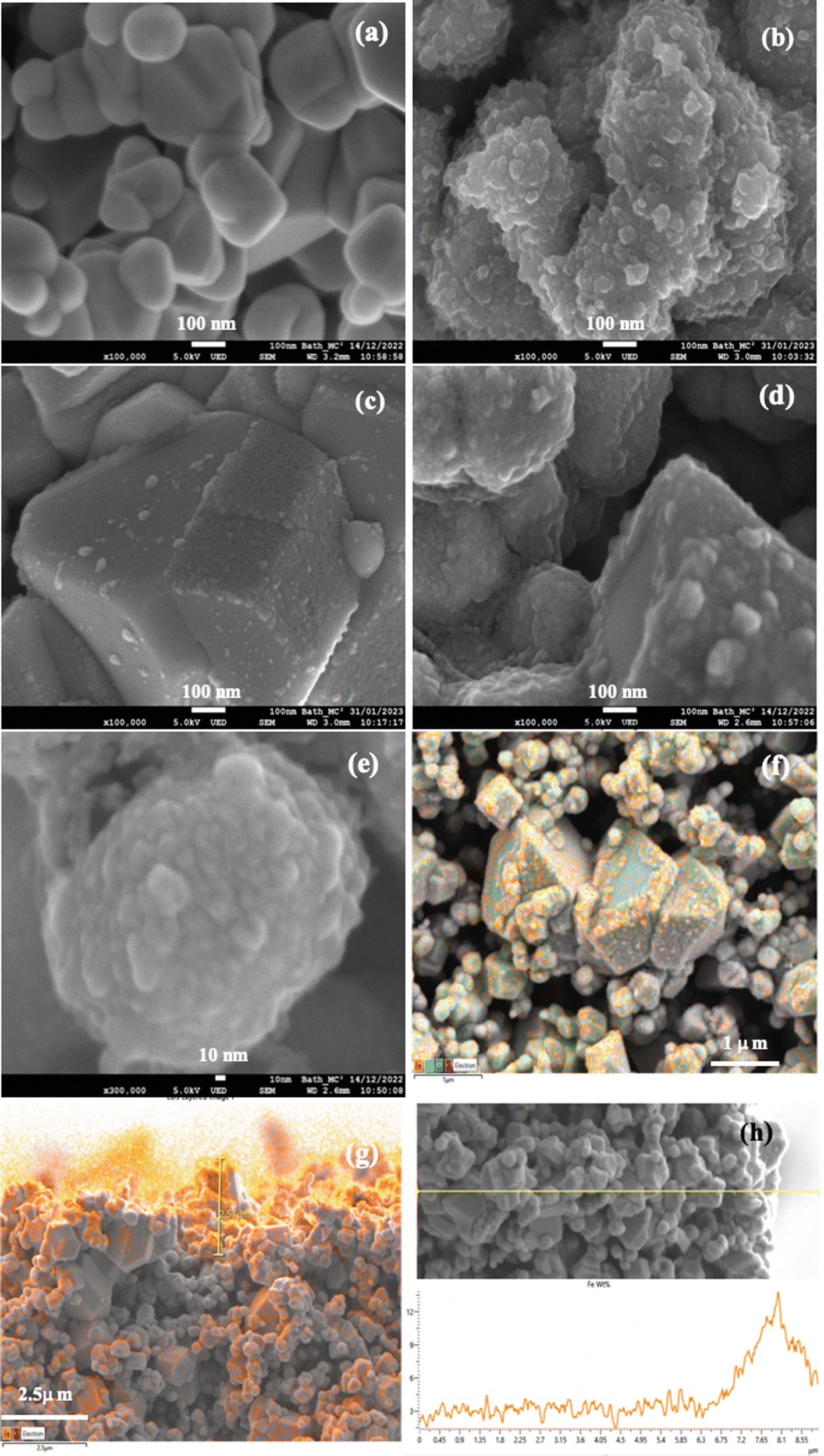 | ||
| Fig. 4 SEM and EDX data for (a) bare CuO–Sb2O5–SnO2 ceramics, (b) ceramics with Prussian Blue deposited for 26 cycles, (c)–(h) ceramics with hematite coating where (c)–(f) show the surface, (g) and (h) – show the cross-section, and (h) shows the intensity changes of the Fe-signal along a yellow line crossing near the surface area. Hematite was formed from PB depositionfor (c) 10 and (d)–(h) 26 cycles. | ||
Prussian blue grows over the entire surface of the grain as a coating with many nanometric agglomerations (Fig. 4(b)). In ceramics exposed to the precursors for 26 treatment cycles, the average thickness of the PB covering is about 100 nm. It is worth noting herein that the grain boundaries and surface in the oxide ceramics are characterized by the presence of lattice mismatches, point defects and impurities, which can possess an electrical charge or cause localized states capable of trapping electrons.50,51 This suggests that the electric charges localized at the grain surface can attract precursor ions during deposition by the directed assembly method. As a result, we visually observe the growth of the Prussian blue coating on the ceramic substrate (Fig. 1(c)). Prussian blue is converted to hematite by subsequent annealing at 600 °C in air for 1 hour.
SEM and EDX data for the CuO–Sb2O5–SnO2 ceramics with hematite coating are presented in Fig. 4(c)–(h). The degree of surface coverage and hematite thickness are dependent on the number of treatment cycles used during the coating growth of Prussian blue, allowing their control by the experimenter. This is demonstrated using SEM micrographs obtained for structures with hematite coating formed after 10 cycles (Fig. 4(c)) and 26 cycles (Fig. 4(d)) of Prussian blue deposition. As can be seen, the thickness of Fe2O3 coating on individual grains is approximately 40 nm after 26 cycles (Fig. 4(d)), whereas it is only around 15 nm after 10 cycles (Fig. 4(c)).
The hematite coating on the surface of the ceramic grain contains some nanometric inhomogeneities which look like some agglomerations or crystal nuclei (Fig. 4(d) and (e)). Probably, this is a result of the initial agglomerations presented in the PB coating (Fig. 4(b)).
The data from EDX analysis reveal the non-uniform distribution of Fe-atoms in the cross-section of the sample. An increased concentration of Fe atoms is observed mainly on the surface of the ceramic substrate, as well as in its near-surface region winding down to about 2–3 μm (Fig. 4(g)). This can also be seen from the intensity changes of the Fe-signal along a line crossing near the surface area (Fig. 4(h)). Thus, the EDX data suggest the presence of a hematite coating on ceramic grains located on the substrate surface and also in the near-surface region. The growth of the Fe2O3 coating inside the substrate is a result of the diffusion of the hematite precursor (Prussian blue precursors) during deposition into the substrate (Fig. 1(d)), promoted by the high porosity of the CuO–Sb2O5–SnO2 ceramics and capillary effects.
SEM data demonstrate that the hematite coating covers the grain-boundary regions between adjacent grains in CuO–Sb2O5–SnO2 ceramics (Fig. 4(d)). This suggests that the appropriate nanometric coating grown by the directed assembly method in the grain boundary regions can enhance or make a more selective sensor response of SnO2-based ceramics, which electrical conductivity is controlled by grain-boundary potential barriers. Coating such ceramics with hematite can increase the potential barrier at the grain boundary.52 This, in turn, facilitates the largest increase in conductance of these materials when reducing gases are introduced. Surface interaction leads to a decrease in the total negative charge at the grain boundary and, accordingly, to a reduction in the height of the grain-boundary potential barrier (ϕ). As a result, the electrical conductance (G) of these ceramics increases and can be detected due to an exponential dependency between G and ϕ.50,51 For example, the application of a nanometric hematite coating could improve the performance of SnO2–Bi2O3–Co3O4–Nb2O5–Cr2O3 ceramics, e.g. in humidity sensing.53 The modification of the potential barriers controlling the conductivity of the structure through the use of surface coatings is a widely employed approach reported in numerous papers.52
The structures reported herein (the CuO–Sb2O5–SnO2 ceramics) are highly electrically conductive materials (120 S m−1) with a linear current–voltage characteristic.40 If the conductivity of oxide ceramics is too high, the grain-boundary potential barriers collapse.51 Therefore, CuO–Sb2O5–SnO2 ceramics are not suitable for sensor applications. However, the photocatalytic response of the obtained CuO–Sb2O5–SnO2 ceramics with functional Fe2O3 coating can be tested in the photoelectrode approach by linear sweep voltammetry.
For this experiment, the junctions formed between CuO–Sb2O5–SnO2 ceramics and the Fe2O3 coating, as well as between hematite and the NaOH electrolyte, can be illustrated using the schematic band diagram shown in Fig. 5. In the illuminated photoelectrode, the absorbed photons excite electrons (e−) from the valence band of hematite to the conduction band (Fig. 5). The holes (h+) generated in the valence band migrate to the surface of hematite, where they participate in the oxidation of water, resulting in the formation of oxygen gas. Simultaneously, the photogenerated electrons in the conduction band move towards the substrate and traverse the junction between the Fe2O3 coating and SnO2-based ceramics, entering the substrate (Fig. 5). They then travel through the conductive ceramic grains and enter the external electrical circuit, progressing towards the counter electrode. At the counter electrode, these electrons participate in the reduction of water, potentially leading to the production of hydrogen gas.
 | ||
| Fig. 5 Energy diagram for PEC water splitting with a hematite photoanode grown on SnO2-based ceramics. The applied external bias, the top of the valence band (Ev), the bottom of the conduction band (Ec), and the Fermi level (EF) are indicated. | ||
The corresponding data from linear sweep voltammetry recorded for bare ceramics and those covered with hematite are presented in Fig. 6(a). The samples of bare ceramics exhibit a photocurrent density of about 0.22 mA cm−2 at 1.23 V vs. RHE under chopped blue LED light (365 nm), while ceramics with hematite coating show a significantly higher photocurrent density of 5.4 mA cm−2 under the same conditions (Fig. 6(a), curves 1 and 3). Thus, the functional Fe2O3-coating increases the photo-response of the material by more than 24 times. The photocurrent in this hematite photoelectrode under AM1.5G radiation reaches 0.12 mA cm−2 at 1.23 V vs. RHE. The corresponding IPCE values estimated at a wavelength of 365 nm are 7.4% for ceramics with hematite coating and 0.3% for bare ceramics. Such a significant difference in the photoresponse of the obtained materials demonstrates the promising potential of nanometric functional coatings formed by the directed assembly method for the engineering of photoelectric properties of SnO2-based ceramics.
 | ||
| Fig. 6 (a) Cyclic voltammetry curves in aqueous 1 M NaOH for bare ceramics (curve 1) and for ceramics with hematite coating under dark conditions (curve 2) and chopped blue LED-radiation (curve 3); (b) the photocurrent density registered under blue LED light at 1.23 V vs. RHE in ceramics with hematite coating grown for different numbers of treatment cycles. | ||
The data presented in Fig. 6(b) show the correlation between the photocurrent and the thickness of the hematite coating for the samples prepared by varying the number of treatment cycles in the deposition of the Prussian blue precursor. As can be seen, the photocurrent increases with increasing cycle numbers from 5 up to 26, reaches a sharp maximum for 26 treatment cycles and then starts to decrease (Fig. 6(b)). This photocurrent behaviour can be explained by the varying thicknesses of the hematite coating obtained in the samples prepared with different numbers of treatment cycles during PB deposition.40 The highest photocurrent is observed when the thickness of the hematite coating in the samples obtained after 26 treatment cycles is about 40 nm (Fig. 4(d)), which is close to the optical thickness for pure hematite (45 nm at a wavelength of 400 nm45). The photoelectrode photocurrent is lowering if: (i) the Fe2O3 coatings become thinner than the optical thickness of hematite (45 nm) and cannot assure a good light absorption;54 or (ii) the Fe2O3-coatings become so thick that the transfer of the photogenerated charge is hindered due to a short diffusion length of the holes in hematite (0.5–1.5 nm55). Thus, an increase in the thickness of hematite coating has the opposite effect on the absorption of light and the transfer of a photogenerated charge. Probably, the Fe2O3 coating formed after 26 treatment cycles has a thickness having the most favourable conditions for charge transfer and light absorption in the obtained porous structures. Thicker films produce lower photocurrents under these conditions. Thus, the photoresponse of the obtained structures strongly depends on the thickness of the hematite coating grown on the surface of the CuO–Sb2O5–SnO2 ceramics.
The electrochemical impedance spectroscopy data presented in Fig. 7 illustrate the impact of the hematite coating on the physicochemical properties of the tested structures, particularly in the low-frequency region (<1 Hz). As observed in the Nyquist plot (Fig. 7(a)), both bare ceramics and those covered with hematite exhibit capacitive reactance, which can be attributed to the porous nature of the ceramic substrate.
 | ||
| Fig. 7 (a) Nyquist and (b,c) Bode plots of the EIS data for different photoanodes: bare ceramics (curves 1 and 2), ceramics covered with hematite in 10 treatment cycles (curves 3 and 4), and in 26 cycles (curves 5 and 6). Curves 1, 3, and 5 were recorded under dark conditions and curves 2, 4, and 6 under blue LED-radiation for the photoelectrodes at 1.23 V vs. RHE in a 1 M NaOH electrolyte. Bode plots of the experimental data in (b and c) are presented by blue dots with a red line and fitting results—by a green line. The used equivalent circuit (transmission line based on model Bisquert#3) is shown in (c). | ||
The impedance plots obtained under dark conditions for ceramics with Fe2O3 coating (Fig. 7(a), curves 3 and 5) are shifted downward along the Z′′-axis compared to the one for bare ceramics (Fig. 7(a), curve 1). Furthermore, this shift is more pronounced in the plot recorded for ceramics with hematite coating deposited for 26 treatment cycles (Fig. 7(a), curve 5) than in the plot for 10 cycles (Fig. 7(a), curve 5). A similar impedance behaviour is also observed for the obtained materials under LED radiation, as seen in Fig. 7(a) with curves 2, 4, and 6. Thus, coating CuO–Sb2O5–SnO2 ceramics with hematite alters the electrical impedance of the material, and these changes are sensitive to the amount of hematite deposited on the surface.
The experimental EIS-data (Fig. 7(a)) were fitted using the Bisquert#3 element56,57 shown in Fig. 7(c), and the obtained results are presented in Table 1. Additionally, Fig. 7(b) and (c) display the fitting plots obtained from the EIS data recorded under light conditions for the hematite photoanode grown in 26 treatment cycles.
| Photoelectrode | Dark conditions | Under LED radiation | ||||||
|---|---|---|---|---|---|---|---|---|
| R1/Ohm | R2/Ohm | R3/Ohm | C/mF | R1/Ohm | R2/Ohm | R3/Ohm | C/mF | |
| Bare ceramics | 5.4 (2.5%) | 1.7 (0.7%) | 5540.0 (23.6%) | 35.9 (0.7%) | 5.2 (2.7%) | 1.9 (0.7%) | 767.6 (3.7%) | 36.4 (0.7%) |
| Ceramics with hematite coating (10 cycles) | 4.6 (2.4%) | 1.8 (0.6%) | 3538.0 (14.4%) | 39.1 (0.6%) | 4.5 (4.4%) | 1.9 (1.0%) | 300.5 (3.2%) | 39.9 (1.1%) |
| Ceramics with hematite coating (26 cycles) | 9.1 (3.7%) | 3.4 (0.9%) | 548.6 (4.3%) | 41.6 (1.1%) | 7.1 (4.5%) | 3.0 (0.9%) | 117.8 (2.0%) | 43.5 (1.4%) |
In the used model (Fig. 7(c)), a resistor R2 in series represents contributions from solution resistance, while the transmission line consists of a set of elements R1 (resistivity in the ceramic substrate), a set of elements R3 (interfacial electron transfer resistance), and a set of capacitors (lumped as Ctotal to represent the total interfacial capacitance). As observed in Fig. 7(b) and (c), the impedance in the high-frequency region is mainly determined by the series resistor R2. In the middle-frequency range, the porous ceramic undergoes charging, resulting in a transmission line behaviour represented by R1 and C elements in the equivalent circuit. In the low-frequency range (<1 Hz), the photoelectrode photoactivity is detected as a semi-circle with R3 representing the charge transfer and C representing the total interfacial capacitance (ceramic and hematite together).
The resulting time constant for charging the photoelectrode interface can be estimated as τ = R2 × Ctotal. In the case of ceramics with a hematite coating formed with 26 treatment cycles, the value of τ is approximately 0.13 s (R2 = 3.0 Ohm and C = 43.5 mF, see Table 1). This τ value restricts the acquisition of high-frequency information but allows for the analysis of data in the low-frequency region (<1 Hz), where water oxidation in the photo-reaction occurs at the interface of the hematite coating and electrolyte.58,59
The resistor R3, representing charge transfer through the electrolyte–photoelectrode interface, exhibits a very high value for the bare ceramics and significantly decreases with hematite deposition (Table 1). This behaviour can be attributed to the enhanced oxygen evolution observed in hematite photoelectrodes compared to bare ceramics.
The notable difference in the photoelectrical response between bare ceramic structures and those with a nanometric hematite coating clearly demonstrates the crucial role of the nanometric functional coating and the promising potential of the directed assembly method for engineering the surface properties of SnO2-based ceramics.
4. Conclusions
We have demonstrated that the directed assembly method can be successfully applied for the controlled growth of nanometric functional hematite coatings on the grain surface in electrically conducting CuO–Sb2O5–SnO2 ceramics. The simplicity and monolayer precision of the directed assembly method make it a promising approach to modify the sensory and photoelectrochemical properties of SnO2-based ceramics. In the future, the microporous nature of Prussian blue might also allow controlled doping for example with metal cations.60Author contributions
A. N. B.: conceptualization, methodology, investigation, writing – original draft, and writing – review & editing. F. M.: conceptualization, methodology, and writing – review & editing.Conflicts of interest
There are no conflicts to declare.Acknowledgements
A. N. B. thanks the National Science and Technology Council of Mexico (CONACYT) for the support provided to this study (the grants # A1-S-20353).References
- X. Liang, J. Zhang, K. Zhang, X. Yang and M. Zhang, Inorg. Chem. Front., 2022, 9, 259 RSC.
- Y. Xu, W. Zheng, X. Liu, L. Zhang, L. Zheng, C. Yang, N. Pinna and J. Zhang, Mater. Horiz., 2020, 7, 1519 RSC.
- Y. Tan, B. Du, C. Liang, X. Guo, H. Zheng, P. Liu, X. Yang, S. Li, B. Jin and J. Sun, Langmuir, 2022, 38, 13833 CrossRef CAS PubMed.
- W. Liu, X. Si, Z. Chen, L. Xu, J. Guo, L. Wei, G. Cheng and Z. Du, J. Alloys Compd., 2022, 919, 165788 CrossRef CAS.
- N. Murata, T. Suzuki, Y. Lin, H. Nitani, Y. Niwa, T. Wada, M. Uo and K. Asakura, ACS Appl. Mater. Interfaces, 2022, 14, 39507 CrossRef CAS PubMed.
- D. C. Patra and S. P. Mondal, ACS Appl. Nano Mater., 2023, 6, 3111 CrossRef CAS.
- B. S. Surendra, K. Gurushantha, K. S. Anantharaju, M. Rudresh, N. Basavaraju, N. Raghavendra, A. A. Jahagirdar, H. M. Somashekarf and H. C. Ananda-Murthy, New J. Chem., 2023, 47, 3978 RSC.
- X. Ma, H. Zhu, L. Yu, X. Li, E. Ye, Z. Li, X. Jun and S. Wang, Nanoscale, 2023, 15, 1609 RSC.
- G. Korotcenkov, B. K. Cho, I. Boris, S. H. Han, Y. Lychkovsky and G. Karkotsky, Sens. Actuators, B, 2012, 174, 586 CrossRef CAS.
- A. S. Tonkoshkur, A. Y. Lyashkov and E. L. Povzlo, Sens. Actuators, B, 2018, 255, 1680 CrossRef CAS.
- C. O. Park, J. W. Fergus, N. Miura, J. Park and A. Choi, Ionics, 2009, 15, 261 CrossRef CAS.
- W. C. Maskell, Solid State Ionics, 2000, 134, 43 CrossRef CAS.
- J. Y. Jung, Y. C. Kim, H. I. Seo, D. T. Chung, Y. J. Kim and J. W. Min, J. Semicond. Dis. Technol., 2005, 4, 1 Search PubMed.
- B. Zhou, C. Li, Y. Zhou, Z. Liu, X. Gao, X. Wang, L. Jiang, M. Tian, F. L. Zhou, S. Jerrams and J. Yu, Compos. Sci. Technol., 2022, 224, 109478 CrossRef CAS.
- T. Reimann, S. Barth, B. Capraro, H. Bartsch and J. Töpfer, Ceram. Int., 2021, 47, 27849 CrossRef CAS.
- L. Steier, I. Herraiz-Cardona, S. Gimenez, F. Fabregat-Santiago, J. Bisquert, S. D. Tilley and M. Grätzel, Adv. Funct. Mater., 2014, 24, 7681 CrossRef CAS.
- M. K. Son, L. Steier, M. Schreier, M. T. Mayer, J. Luo and M. Grätzel, Energy Environ. Sci., 2017, 10, 912 RSC.
- J. B. Pan, X. Liu, B. H. Wang, Y. A. Chen, H. Y. Tan, J. Ouyang, W. Zhou, S. Shen, L. Chen, C. T. Au and S. F. Yin, Appl. Catal., B, 2022, 315, 121526 CrossRef CAS.
- H. Han, J. Chen, L. Wen and J. Liu, Catal. Lett., 2022, 152, 3294 CrossRef CAS.
- S. S. Patil, M. A. Johar, M. A. Hassan, D. R. Patil and S. W. Ryu, Sol. Energy, 2019, 178, 125 CrossRef CAS.
- C. Zhen, J. C. Yu, G. Liu and H. M. Cheng, Chem. Commun., 2014, 72, 10416 RSC.
- K. C. Bedin, B. Mouriño, I. Rodríguez-Gutiérrez, J. B. Souza-Junior, G. T. Santos, J. Bettini, C. A. R. Costa, L. Vayssieres and F. L. Souza, Chin. J. Catal., 2022, 5, 1247 CrossRef.
- J. H. Kim, D. Hansora, P. Sharma, J. W. Jang and J. S. Lee, Chem. Soc. Rev., 2019, 48, 1908 RSC.
- S. Kim, M. A. Mahadik, A. Periyasamy, W. S. Chae, J. Ryu, S. H. Choi and J. S. Jang, Catal. Sci. Technol., 2021, 11, 3141 RSC.
- Y. Li, G. Liu, D. Jia, C. Li, L. Wang, J. Zheng, X. Liu and Z. Jiao, Catal. Lett., 2019, 149, 19 CrossRef CAS.
- R. C. Millward, C. E. Madden, I. Sutherland, R. J. Mortimer, S. Fletcher and F. Marken, Chem. Commun., 2001, 1994 RSC.
- K. Thorkelsson, P. Bai and T. Xu, Nano Today, 2015, 10, 48 CrossRef CAS.
- E. V. Amadi, A. Venkataraman and C. Papadopoulos, Nanotechnology, 2022, 33, 132001 CrossRef PubMed.
- J. C. Love, L. A. Estroff, J. K. Kriebel, R. G. Nuzzo and G. M. Whitesides, Chem. Rev., 2005, 105, 1103 CrossRef CAS PubMed.
- V. M. Rotello, A. K. Boal, F. Ilhan, J. E. DeRouchey, T. Thurn-Albrecht and T. P. Russell, Nature, 2000, 404, 746 CrossRef PubMed.
- B. Dong, T. Zhou, H. Zhang and C. Y. Li, ACS Nano, 2013, 7, 5192 CrossRef CAS PubMed.
- B. A. Grzybowski, C. E. Wilmer, J. Kim, K. P. Browne and K. J. M. Bishop, Soft Matter, 2009, 5, 1110 RSC.
- Z. Cai, B. Liu, X. Zou and H. M. Cheng, Chem. Rev., 2018, 118, 6091 CrossRef CAS PubMed.
- S. Reculusa and S. Ravaine, Chem. Mater., 2003, 15, 598 CrossRef CAS.
- P. Moni, A. Al-Obeidi and K. K. Gleason, Beilstein J. Nanotechnol., 2017, 8, 723 CrossRef CAS PubMed.
- H. Assadi, H. Kreye, F. Gärtner and T. Klassen, Acta Mater., 2016, 116, 382 CrossRef CAS.
- Z. Zhang, B. Peng, X. Ji, K. Pei and P. K. L. Chan, Adv. Funct. Mater., 2017, 27, 1703443 CrossRef.
- X. Suo, S. Yin, M. P. Planche, T. Liu and H. Liao, Surf. Coat. Technol., 2015, 268, 90 CrossRef CAS.
- A. N. Bondarchuk, I. Corrales-Mendoza, J. A. Aguilar-Martínez, U. M. García-Pérez and F. Marken, Catal. Commun., 2023, 174, 106593 CrossRef CAS.
- A. N. Bondarchuk, I. Corrales-Mendoza, F. Marken, L. Á. Arellanes-Mendoza, J. A. Aguilar-Martínez, L. G. Silva-Vidaurri, G. Curiel-Olivares and F. Montejo-Alvaro, Sol. Energy Mater. Sol. Cells, 2021, 221, 110886 CrossRef CAS.
- L. Z. Liu, T. H. Li, X. L. Wu, J. C. Shen and P. K. Chu, J. Raman Spectrosc., 2012, 43, 1423 CrossRef CAS.
- R. G. Drabeski, J. V. Gunha, A. Novatski, G. B. de Souza, S. M. Tebcherani, E. T. Kubaski and D. T. Dias, Vib. Spectrosc., 2020, 109, 103094 CrossRef CAS.
- J. Geurts, S. Rau, W. Richter and F. J. Schmitte, Thin Solid Films, 1984, 121, 217 CrossRef CAS.
- A. Diéguez, A. Romano-Rodríguez, A. Vilà and J. R. Morante, J. Appl. Phys., 2001, 90, 1550 CrossRef.
- D. L. A. de Faria, S. V. Silva and M. T. de Oliveira, J. Raman Spectrosc., 1997, 28, 873 CrossRef CAS.
- J. Deng, X. Xu, J. Wang, L. Yuanyan and H. Bifeng, Catal. Lett., 1995, 32, 159 CrossRef CAS.
- I. V. Chernyshova, M. F. Hochella and A. S. Madden, Phys. Chem. Chem. Phys., 2007, 9, 1736 RSC.
- A. M. Jubb and H. C. Allen, ACS Appl. Mater. Interfaces, 2010, 2, 2804 CrossRef CAS.
- M. J. Massey, U. Baier, R. Merlin and W. H. Weber, Phys. Rev. B: Condens. Matter Mater. Phys., 1990, 41, 7822 CrossRef CAS PubMed.
- G. E. Pike and C. H. Seager, J. Appl. Phys., 1979, 50, 3414 CrossRef CAS.
- D. R. Clarke, J. Am. Ceram. Soc., 1999, 82, 485 CrossRef CAS.
- D. R. Miller, A. A. Sheikh and P. A. Morris, Sens. Actuators, B, 2014, 204, 250 CrossRef CAS.
- I. Skuratovsky, A. Glot, E. Di Bartolomeo, E. Traversa and R. Polini, J. Eur. Ceram. Soc., 2004, 24, 2597 CrossRef CAS.
- L. A. Marusak, R. Messier and W. B. White, J. Phys. Chem. Solids, 1980, 41, 981 CrossRef CAS.
- F. Le Formal, K. Sivula and M. Gratzel, J. Phys. Chem. C, 2012, 51, 26707 CrossRef.
- J. Biquert, Phys. Chem. Chem. Phys., 2000, 2, 4185 RSC.
- J. Bisquert, G. Garcia-Belmonte, F. Fabregat-Santiago and A. Compte, Electrochem. Commun., 1999, 1, 429 CrossRef CAS.
- K. G. U. Wijayantha, S. Saremi-Yarahmadia and L. M. Peter, Phys. Chem. Chem. Phys., 2011, 13, 5264 RSC.
- T. Lopes, L. Andrade, F. Le Formal, M. Gratzel, K. Sivula and A. Mendes, Phys. Chem. Chem. Phys., 2014, 16, 16515 RSC.
- X. Lv, G. T. Zhang, M. L. Wang, G. Q. Li, J. J. Deng and J. Zhong, Phys. Chem. Chem. Phys., 2022, 3, 1406 Search PubMed.
| This journal is © the Owner Societies 2023 |