
 Open Access Article
 This Open Access Article is licensed under a
 Creative Commons Attribution 3.0 Unported Licence
Ab initio simulations of ultrashort laser pulse interaction with Cl–Si(100): implications for atomic layer etching
Peizhi
Wang
 a and
Fengzhou
Fang
*ab
a and
Fengzhou
Fang
*ab
aCentre of Micro/Nano Manufacturing Technology (MNMT-Dublin), University College Dublin, Dublin 4, Ireland. E-mail: fengzhou.fang@ucd.ie
bState Key Laboratory of Precision Measuring Technology and Instruments, Laboratory of Micro/Nano Manufacturing Technology (MNMT), Tianjin University, Tianjin, 300072, China
First published on 26th July 2023
Abstract
Due to the remarkable resistance of SiCl against photo-induced desorption, achieving atomic layer etching (ALE) of Cl–Si(100) through a laser-based method has remained a formidable challenge. In this study, we investigate the interaction between ultrashort laser pulses and the Cl–Si(100) surface via ab initio simulations that combine real-time time-dependent density functional theory and molecular dynamics. Our results demonstrate the direct desorption of the stubborn SiCl layer through the application of appropriate femtosecond laser pulses. Notably, the desorption process is enhanced by pulses with higher laser intensity, shorter wavelength, and longer pulse duration. There is a threshold intensity beyond which the SiCl can be directly desorbed under laser pulses with a wavelength of 488 nm and a pulse duration of 40 ℏ eV−1 (26.3 fs). Analysis of electron localization function reveals a critical bond breaking length of 2.98 Å between Si–Si, connecting SiCl to the bulk material. The time evolution of bond lengths and forces reveals that the desorption of SiCl is primarily driven by repulsive forces generated within the Si–Si bond. Furthermore, electron density difference analysis and Keldysh factor calculations indicate that these repulsive forces arise from multiphoton ionization. This study provides crucial atomic-level insights into the interaction of ultrashort laser pulses with Cl–Si(100), thereby propelling the advancement of laser-induced atomic layer etching techniques.
I. Introduction
The production of chips using 3 nm process technology with Gate-All-Around (GAA) transistor architecture has recently begun.1 As the feature size continues to scale down, the high-volume manufacturing of next-generation nanoelectronics is moving towards the era of atomic and close-to-atomic scale in which every atom of functional structures on devices becomes critical.2–6 To enable structure fabrication towards atomic and close-to-atomic scale manufacturing (ACSM), various techniques are being explored, and atomic layer etching (ALE) is considered as one of the promising ones, as it allows for the theoretical removal of a single atomic layer within a single processing cycle.7–13Among current ALE approaches, laser-induced ALE offers a more efficient removing process (compared to thermal ALE) and provides enhanced control over reactions (compared to plasma ALE). In the early 1990s, investigation was conducted on the chemical interaction of Cl-containing gases with Si surfaces under laser pulses, and the etching rate could be reduced to nearly monoatomic layer per pulse as reported in the ref. 14. Subsequently, laser-induced ALE of GaAs was studied, employing Cl2 gas for surface modification.15,16 Notably, studies17,18 revealed the existence of a laser fluence threshold that distinguishes between atomic layer removal and ablation. Beyond this threshold, the process transitions into ablation rather than precise atomic layer removal. Despite the initial progress, the laser-induced ALE approach remained relatively undeveloped until 2018 when it found successful application in layer thinning of layered materials like MoS2 and MoTe2 due to their weak interlayer interaction (van der Waals forces).19–21 However, the application of laser-induced ALE remains a challenge when it comes to bulk materials such as silicon (Si), which has tightly bound covalent bonds. In ALE of Si, chlorine (Cl) is typically used to weaken the Si–Si bonds prior to subsequent removal, forming SiCl as the primary product during modification on surfaces.7 Unfortunately, the SiCl layer on Cl–Si(100) is stable against conventional laser irradiation,22,23 making it difficult to desorb directly without damaging bulk atoms. To address this challenge, the use of ultrashort laser pulses was24–27 demonstrated to effectively remove the SiCl layer through electronic excitation. Despite these advancements, the laser-induced ALE approach is still in the development stage, and the fundamental mechanism of interaction between ultrashort laser and Cl–Si (100) is yet to be fully understood.
In the present work, we investigate the ultrashort laser pulse interaction with Cl–Si(100) by ab initio simulations combining real-time time-dependent density functional theory (rt-TDDFT) and molecular dynamics (MD). The simulation method has been successfully utilized in exploring the atomic-level mechanisms involved in processes such as molecular dissociation,28,29 field evaporation,26,30 and adsorbates desorption31,32 induced by ultrashort laser pulses. By varying laser parameters such as laser intensity, wavelength, and pulse duration, we systematically analyze the desorption dynamics of SiCl from Cl–Si(100). The underlying mechanisms are elucidated through analysis of the evolution of bond length and force, electron density difference, and ionization regimes, with the goal of advancing the development of laser-induced ALE.
II. Laser-induced ALE and computational methods
Fig. 1(a) illustrates the schematic of the laser-induced ALE approach. Initially, the top atomic layer of Si is modified by Cl atoms to form a modified layer, where the primary product is SiCl, similar to conventional plasma or thermal ALE approaches. During modification, the reaction is self-limiting since the formed SiCl layer blocks further reaction once all surface Si atoms are terminated by Cl. Next, a pulsed laser is introduced to directly remove the modified layer through the laser-induced desorption of SiCl. Repeating this cycle allows for layer-by-layer removal of Si for direct writing of structures. Fig. 1(b) displays the atomic force microscopy (AFM) images of Si surfaces that underwent one and three cycles of pulsed laser-induced ALE, respectively. These experiments achieved a consistent etching depth of ∼0.85 nm per cycle, indicating the significant potential of laser-induced ALE approach for precise material removal. | ||
| Fig. 1 (a) Schematic of laser-induced ALE approach. The top atomic layer of Si is first modified by Cl to form a modified SiCl layer, which is then selectively removed under the irradiation of laser pulses, (b) AFM image of Si topography after pulsed laser-induced ALE process, 1× and 3× represent one and three cycles of ALE, respectively, a consistent ∼0.85 nm etching depth per cycle was achieved.25 | ||
Femtosecond laser (fs-laser) generates much shorter pulses than nanosecond and picosecond lasers and thus enables a more precise and controllable material processing. Herein, the ab initio dynamics of interaction between fs-laser and Cl–Si(100) are presented by combining rt-TDDFT and MD within Ehrenfest dynamics. Time-dependent Kohn–Sham equations33,34 are used to calculate the electronic structure of this system,
 | (1) |
 | (2) |
![[thin space (1/6-em)]](https://www.rsc.org/images/entities/char_2009.gif) sin(ωt)fenv(t)
sin(ωt)fenv(t)![[k with combining circumflex]](https://www.rsc.org/images/entities/b_char_006b_0302.gif) , E0 is laser field magnitude, and ω are polarization direction and frequency of laser, respectively, fenv is the envelope function.
, E0 is laser field magnitude, and ω are polarization direction and frequency of laser, respectively, fenv is the envelope function.
The ion dynamics are computed by classic MD simulations within Ehrenfest dynamics where the kinetic energy contributions are separated, and the time-dependent ion motion equation becomes,31,35
 | (3) |
This paper utilizes the OCTOPUS 11.4 code36 for all ab initio simulations, with electron–ion interaction described by pseudopotentials proposed by Hartwigsen, Goedecker, and Hutter with the local density approximation (LDA) functional.26,37 We tested three commonly used pseudopotentials in OCOTOPUS, namely pseudodojo_pbe (Perdew–Burke–Ernzerhof (PBE)version of the dojo pseudopotentials), pseudodojo dojo_lda (LDA version of the dojo pseudopotentials), and hgh_lda (Hartwigsen-Goedecker-Hutter LDA pseudopotentials), and found that they produce similar bond-length evolution curves (see Fig. 9 in Appendix). This is consistent with previous research indicating that LDA can describe the electronic structure of Si reasonably well.38
The simulation box dimension used in this study are 20 × 20 × 20 Å3 and the mesh size is 0.2 Å (the convergency test is shown in Fig. 10 in Appendix). The propagation time is 300 ℏ eV−1 (197.4 fs) and the step is 2 × 10⁻³ ℏ eV−1 (0.0013 fs), where 1 ℏ eV−1 ≈ 0.658 fs. The numerical calculation stability with time is tested and shown in Fig. 11 in Appendix. The influence of cluster size is investigated using two clusters of chlorinated Si shown in Fig. 2. The time evolution of the Si1–Si2 bond within the two clusters are monitored (see Fig. 12 in Appendix) and the smaller one is selected for subsequent calculations to save computational costs. The Si atoms on the topmost layer are terminated with Cl atom to form SiCl for desorption. All dangling Si bonds present on the edge and bottom sides of the cluster are passivated with H atoms to eliminate the effects of dangling bonds that do not exist in the actual system. Atoms – Si1, Si4, Cl1, and Cl4 – can move with time propagation under laser pulses. The remaining atoms are fixed to preserve the general geometric structure of the surface, as well as to prevent drifting of the whole cluster under the applied field during rt-TDDFT calculations.26,31,35 The polarization direction of the pulsed laser is along the z-axis. The calculated bond lengths of Si–Cl and Si1–Si3 before laser irradiation are 2.088 and 2.356 Å, respectively, in agreement with previous literature results.39,40
 | ||
| Fig. 2 Cluster models for calculation: (a) Si25Cl4H28, (b) Si35Cl6H36. Yellow, white, and blue atoms refer to silicon, hydrogen and chlorine, respectively. | ||
III. Results and discussion
A. Effect of laser intensity
The effects of various laser parameters (such as laser intensity, wavelength, and pulse duration) on desorption is studied by examining the electron–ion dynamics subjected to intensive fs-laser pulses. Firstly, a sequence of simulations is conducted with fs-laser pulses with a 488 nm wavelength (2.54 eV) and a Gaussian envelope function, fenv(t) = exp(−(t − t0)2/(2τ02)). The peak position t0 and pulse width/duration τ0 are set at 100 ℏ eV−1 (65.8 fs) and 40 ℏ eV−1 (26.3 fs), respectively. The magnitude of laser field E0 changes from 2.3 V Å−1 to 2.8 V Å−1 with an interval of 0.1 V Å−1, resulting in corresponding laser intensity I ranging from 7.02 × 10¹³ W cm−2 to 1.04 × 10¹⁴ W cm−2, as shown in Table 1. According to the extinction coefficient,41 the penetration depth of 488 nm light into silicon is calculated to be 0.485 μm.| Magnitude E0 (V Å−1) | 2.8 | 2.7 | 2.6 | 2.5 | 2.4 | 2.3 |
| Intensity I (1013 W cm−2) | 10.4 | 9.67 | 8.97 | 8.29 | 7.64 | 7.02 |
| Fluence F (J cm−2) | 2.43 | 2.26 | 2.09 | 1.93 | 1.78 | 1.64 |
Fig. 3 presents the final snapshots of the Cl–Si(100) system at t = 300 ℏ eV−1 (197.4 fs) under fs-laser pulses with various E0 or I. The upper three panels depict the snapshots with the magnitude E0 of 2.8, 2.7, and 2.6 V Å−1, respectively, while the lower three panels correspond to E0 being 2.5, 2.4, and 2.3 V Å−1, respectively. It is observed that the SiCl molecule remains stable against laser irradiation when E0 is below 2.5 V Å−1 (or the intensity I below 8.29 × 10¹³ W cm−2). However, when E0 exceeds 2.6 V Å−1, the Cl–Si(100) system becomes unstable, leading to the breaking of the Si1–Si2 and Si1–Si3 bonds between SiCl and bulk Si, and the subsequent direct desorption of SiCl. These findings suggest that fs-laser pulses with a suitable intensity can remove the SiCl layer on Si directly, making them suitable for ALE of Si for direct writing of atomically precise structures. Furthermore, the results indicate that the Si–Cl bond exhibits higher resistance to laser irradiation than the Si–Si bond, implying that the SiCl may be desorbed from the surface while preserving the integrity of the Si–Cl bonds. These observations are consistent with the experimental outcomes from pulsed laser irradiation of chlorinated Si substrates.24
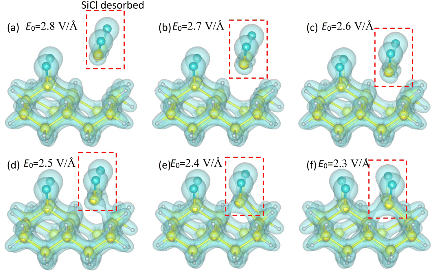 | ||
| Fig. 3 Snapshots of the Cl–Si(100) system at t = 300 ℏ eV−1 (197.4 fs) under fs-laser pulses with the magnitude E0 of (a) 2.8 V Å−1, (b) 2.7 V Å−1, (c) 2.6 V Å−1, (d) 2.5 V Å−1, (e) 2.4 V Å−1, and (f) 2.3 V Å−1. The corresponding intensities are shown in Table 1. | ||
The bonding energy between Si–Cl was calculated to be 4.46 eV, while the average bonding energy between chlorinated Si and bulk Si is 1.96 eV. This explains why the Si–Cl bond are more stable than the Si–Si bond from a ground state perspective. Besides, Fig. 3 shows that the degree of bond dissociation is slightly more severe for the Si1–Si2 bond compared to the Si1–Si3 bond. This difference is due to the boundary (or environmental) conditions. The right side of the Si3 (or the right side of the Si1Cl1 molecule) is a free space boundary (with no atoms appearing), while the left side is occupied by the cluster. Thus, the Si1Cl1 molecule is easier to move towards the free right side, leading to a slightly more severe dissociation of the Si1–Si2 bond.
Time evolution of the Si1–Si2 bond under laser pulses with various magnitude E0 or intensity I is presented in Fig. 4. It shows that the Si1–Si2 bond is highly sensitive to laser intensity and that a higher magnitude of E0 leads to a faster bond elongation and eventually dissociation. Specifically, when E0 is above 2.6 V Å−1, the value of bond length increases dramatically with time evolution, indicating that the Si1–Si2 bond is broken at this time. When E0 is lower than 2.5 V Å−1, the bond length increases gradually and smoothly with time evolution, indicating that the Si1–Si2 bond would continue to exist, as shown in Fig. 4(b). With time extending to 500 ℏ eV−1 (329 fs), the Si1–Si2 bond starts to retract after its initial lengthening, vibrating around its equilibrium position rather than dissociating directly if E0 is not sufficiently large. The threshold magnitude E0 = 2.6 V Å−1 corresponds to the fluence of 2.09 J cm−2, which is approximately an order of magnitude higher than the experimental threshold shown in Fig. 1(b). The high difference could be attributed two reasons.42–44 One is that the small size of the cluster used in calculations has a more discrete nature of electronic levels than the bulk used in experiments. The second reason is that the bond dissociation probability in calculations is always 1 at the threshold fluence, while in experiments the dissociation follows a probability distribution.
 | ||
| Fig. 4 Time evolution of the Si1–Si2 bond under fs-laser pulses with the propagation time of (a) 300 ℏ eV−1 (197.4 fs) and (b) up to 500 ℏ eV−1 (329 fs). | ||
Additionally, Fig. 4(b) suggests that the propagation time of 300 ℏ eV−1 (197.4 fs) is sufficient to simulate the bond breakage of Si1–Si2. It is worth noting that the bond length exhibits negligible change during the first 120 ℏ eV−1 (79.0 fs) and then begins to increase sharply at t = 120–150 ℏ eV−1 (79.0–98.7 fs). The reason for this behavior is the loss of electrons within Si1–Si2 bond under laser pulses, which will be discussed in more detail in the following mechanism analysis section.
The electron localization function (ELF) of the Cl–Si(100) system is present in Fig. 5 for further analysis of the bonding nature between SiCl and bulk. ELF (fELF) is defined as a positive quantity that varies between 0 and 1 and can be evaluated using eqn (4)–(6).45 High ELF values indicate that electrons are highly localized within that region and vice versa.46 For a clearer visualization, the 2D cross-section consisting of the Si1–Si2 and Si1–Si3 bonds (i.e., the red plane in Fig. 2) is used to display the ELF results.
 | (4) |
 | (5) |
 | (6) |
 | ||
| Fig. 5 (a) ELF of the Cl–Si(100) system at t = 300 ℏ eV−1 (329 fs) under laser pulses with E0 changing from 2.8 V Å−1 to 2.3 V Å−1, (b) time evolution of ELF under laser pulses with E0 = 2.6 V Å−1. The 2D cross-section plane is formed by the bond lines Si1–Si2 and Si1–Si3, which is marked as the red plane in Fig. 2. | ||
As shown in Fig. 5(a), when E0 is lower than 2.5 V Å−1, electrons within the Si1–Si2 bond are highly located, indicating that the Si1–Si2 bond remains in its covalent state, which is consistent with the aforementioned results. However, when E0 is above 2.6 V Å−1, the localization of electrons within the Si1–Si2 bond decreases significantly and even disappears, indicating bond breakage. Fig. 5(b) shows the time evolution of ELF under laser pulses with E0 = 2.6 V Å−1. It can be observed that localized electrons within the Si1–Si2 bond turn to disappear at t = 240 ℏ eV−1 (157.9 fs), which corresponds to a bond length of 2.98 Å. This critical bond length is therefore considered to be the threshold for bond breakage.
B. Effect of wavelength and pulse duration
The effect of laser wavelength on desorption dynamics of SiCl is explored by a series of simulations using fs-laser pulses with the wavelength changing from 400 nm to 800 nm with an interval of 100 nm. The applied pulses have the same intensity of 8.97 W cm−2 (or E0 = 2.6 V Å−1) and pulse width of 40 ℏ eV−1 (26.3 fs). As shown in Fig. 6(a), the degree of bond breakage increases with decreasing wavelength, consistent with the simulation findings on hydrogen atom desorption from Si surfaces.31 This observation can be easily explained by considering that a shorter wavelength corresponds to a higher energy level for a photon. For wavelengths longer than 500 nm, the Si1–Si2 bond remains stable against laser irradiation. However, as the wavelength decreases below 500 nm, the Si1–Si2 bond becomes increasingly unstable and eventually breaks, leading to the SiCl desorption. | ||
| Fig. 6 Time evolution of the Si1–Si2 bond under fs-laser pulses with different (a) wavelengths and (b) pulse durations, 300 ℏ eV−1 ≈ 197.4 fs. | ||
The pulse duration/width can also affect the direct fs-laser-induced ALE processes. To examine this effect, we conduct simulations using laser pulses with widths of 20 ℏ eV−1 (13.2 fs), 30 ℏ eV−1 (19.7 fs), and 40 ℏ eV−1 (26.3 fs), respectively, while keeping the peak position t0 at 100 ℏ eV−1 (65.8 fs). These pulses have identical intensity and wavelength. As expected, the desorption of SiCl becomes increasingly favorable with longer pulse durations. At a shorter pulse duration (20 ℏ eV−1 or 13.2 fs), the energy adsorbed is not sufficient to break the Si1-Si2 bond, resulting in a final bond length of only 2.58 Å at t = 300 ℏ eV−1 (197.4 fs), which is below the critical value of 2.98 Å.
C. Underlying mechanism
To elucidate the underlying mechanism of fs-laser-induced ALE, the time evolution of the z-axis force exerted on the Si atom of the SiCl molecule is calculated using eqn (3) and depicted in Fig. 7. The motivation behind analyzing this force is primarily driven by our focus on studying the evolution of bond length in the Si–Si bond between the chlorinated Si atom and bulk Si. It shows that, regardless of laser intensity, wavelength, and pulse duration, the force oscillates rapidly during the first 100–120 ℏ eV−1 (79.0–98.7 fs) along with the rapid oscillating fs-laser field. After that, the repulsive forces between SiCl and the bulk increase significantly and maintain positive values, depending on the applied laser parameters. High intensities, short wavelengths, and long pulse durations lead to large repulsive forces. Specifically, forces under the fs-laser pulses with a 400 nm wavelength can reach up to 4.24 eV Å−1, leading to the desorption of SiCl. These high repulsive forces start from t = 120–150 ℏ eV−1 (79.0–98.7 fs), coinciding with the time when the bond length starts to increase sharply in Fig. 4 and 6. This further confirms the conclusion that repulsive forces under laser irradiation lead to the desorption of SiCl. As time continues to propagate, the value of repulsive forces gradually decreases because the Coulomb force between the corresponding atoms decreases with SiCl moving away from the surface. | ||
| Fig. 7 Time evolution of the z-axis force acting on SiCl under fs-laser pulses with different (a) intensities, (b) wavelengths, and (c) pulse durations, 300 ℏ eV−1 ≈ 197.4 fs. | ||
To figure out the origin of these repulsive forces, we analyze the electron density difference of the Cl–Si(100) system between t = 0 and 140 ℏ eV−1 (92.1 fs), as shown in Fig. 8. The density difference is calculated as Δn(r,t) = n(r,t) − n(r,t0), where n(r,t) is the electron density at time t. The reason for selecting t = 140 ℏ eV−1 (92.1 fs) is that it falls within the starting period of t = 120–150 ℏ eV−1 (79.0–98.7 fs), the bond length does not increase significantly and the structural change of the simulated system can be neglected. At high intensities, E0 = 2.8 V Å−1 and 2.6 V Å−1, the Si1-Si2 bond loses electrons due to laser-induced ionization, whereas at low intensities, E0 = 2.4 V Å−1, the electron loss within these bonds is not noticeable. The observed electron loss explains the generation of these repulsive forces. The forces between atoms come from three components: the external potential-induced force, ion–ion interaction, and ion–electron interaction, as described in eqn (3). The loss of electrons affects the ion–electron interaction, i.e., the third term on the right-hand side of eqn (3), which reduces the attraction of electrons on SiCl and, therefore, leads to the repulsive forces between SiCl and bulk. It is worth noting that electron accumulation was observed near the Si atoms as depicted by the blue color in the bottom panels of Fig. 8. However, the impact of the accumulated electrons on the strengthening of the Si–Si bond is less significant compared to the bond weakening impact caused by electron loss within the Si–Si bond. This is attributed to the fact that the accumulated electrons have a reduced ability to attract the Si atom on the opposite side of the Si–Si bond. Consequently, the electron loss within the Si–Si bond dominates the bond-breaking process.
 | ||
| Fig. 8 Electron density difference of the Cl–Si(100) system at t = 140 ℏ eV−1 (92.1 fs) subjected to fs-laser pulses with (a) E0 = 2.8 V Å−1, (b) E0 = 2.6 V Å−1, and (c) E0 = 2.4 V Å−1. The upper three panels are the 3D graphics and the bottom panels correspond to the 2D cross-section graphics, where the red region represents electron loss. | ||
The ionization mechanism subjected to these intensive fs-laser pulses is further investigated by calculating the Keldysh factor γ:47γ = ωa(2meIp)1/2/(eE0), where ωa is the laser angular frequency, me and e are the mass and charge of an electron, respectively, Ip is the ionization energy, E0 is the magnitude of laser field. γ > 1 indicates that the multiphoton ionization dominates the ionization process, while γ < 1 corresponds to the tunneling ionization-dominated process. The calculated γ for the cases of E0 = 2.8 V Å−1 and 2.6 V Å−1 are 5.89 and 4.36, respectively. Additionally, the ionization energy was determined by analyzing the Coulomb energy evolution under laser irradiation.28 The calculated values for the ionization energy were calculated to be 2.79 Ha and 4.36 Ha, corresponding to the cases where E0 is 2.8 V Å−1 and 2.6 V Å−1, respectively. The obtained Keldysh factors are much larger than 1, indicating that multiphoton ionization dominates the fs-laser-induced ALE processes. The electron loss due to multiphoton ionization leads to repulsive forces between SiCl and bulk, driving SiCl moving away from the surface and ultimately completing the material removal in ALE of Si.
IV. Conclusions
Ab initio simulations combining rt-TDDFT and MD were performed to investigate the interaction between ultrashort laser pulses and Cl–Si(100) surfaces for advancing laser-induced ALE techniques. The main findings of this study can be summarized as follows:(1) Ab initio simulations demonstrated that the difficult-to-remove SiCl layer can be directly desorbed by appropriately tuned ultrashort laser pulses. The threshold intensity for SiCl desorption was calculated as 8.97 × 10¹³ W cm−2 (or E0 = 2.6 V Å−1) using laser pulses with a wavelength of 488 nm and a pulse duration of 40 ℏ eV−1 (26.3 fs). Various laser parameters can affect the desorption process, with larger intensities, shorter wavelengths, and longer pulse durations found to facilitate the SiCl desorption. Note that the calculated threshold intensity is approximately an order of magnitude higher than the experimental value due to the limitation of the applied rt-TDDFT calculation method.
(2) The effect of laser pulses on bonding status was analyzed by examining the time evolution of the Si1–Si2 bond between SiCl and bulk, along with the electron localization function. The critical bond length of Si1–Si2 for bond breaking was found to be 2.98 Å. Repulsive forces generated within the Si1–Si2 bond are responsible for the desorption of SiCl. Specifically, under laser pulses with a wavelength of 400 nm, an intensity of 8.97 × 10¹³ W cm−2, and a pulse duration of 40 ℏ eV−1 (26.3 fs), the peak repulsive force value reached 4.24 eV Å−1, which results in the SiCl desorption from the surface.
(3) An analysis of electron density difference revealed that the generation of these repulsive forces is related to the electron loss within the Si1–Si2 bond under fs-laser pulses. The Keldysh factors γ, which provide a measure of the dominant ionization mechanism, were calculated to be 5.89 and 4.36 for E0 = 2.8 V Å−1 and 2.6 V Å−1, respectively. These results indicated that multiphoton ionization dominates the ionization process during laser-induced ALE of Si.
This work provides a fundamental insight into the atomic-level mechanism of laser-induced ALE process. These findings have the potential to advance the development of ALE techniques for the fabrication of atomically precise structures with high efficiency and controllability, while avoiding damage to the material surface.
Conflicts of interest
There are no conflicts of interest to declare.Appendix
Convergency and stability test
 | ||
| Fig. 9 Time evolution of the Si1–Si2 bond under fs-laser pulses with an intensity of 8.97 × 10¹³ W cm−2, a wavelength of 488 nm, and a pulse width of 40 ℏ eV−1 (26.3 fs). Three commonly used pseudopotentials in OCTOPUS are tested: pseudodojo_pbe (Perdew–Burke–Ernzerhof (PBE)version of the dojo pseudopotentials), pseudodojo dojo_lda (LDA version of the dojo pseudopotentials), and hgh_lda (Hartwigsen–Goedecker–Hutter LDA pseudopotentials) | ||
 | ||
| Fig. 10 Ground state energy of the simulation system with mesh size ranging from 0.18 Å to 0.320 Å. | ||
 | ||
| Fig. 11 Total energy of the simulation system within 200 running steps (the time step is 2 × 10⁻³ ℏ eV−1). Energy values are stable with running steps. | ||
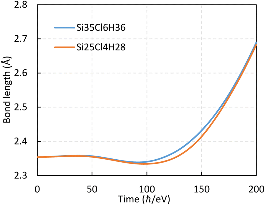 | ||
| Fig. 12 Time evolution of the Si1–Si2 bond in different clusters under fs-laser pulses with an intensity of 8.97 × 10¹³ W cm−2, a wavelength of 488 nm, and a pulse width of 40 ℏ eV−1 (26.3 fs). | ||
Acknowledgements
The work is support by the Science Foundation Ireland (SFI) (No. 15/RP/B3208). The authors would like to thank Marco Castelli, Ning Huang, Zhichao Geng, and Chenghao Chen for valuable discussions.References
- Samsung Newsroom, Samsung Begins Chip Production Using 3nm Process Technology With GAA Architecture. https://news.samsung.com/global/samsung-begins-chip-production-using-3nm-process-technology-with-gaa-architecture.
- D. Akinwande, C. Huyghebaert, C. H. Wang, M. I. Serna, S. Goossens, L. J. Li, H. S. Wong and F. H. Koppens, Nature, 2019, 573, 507–518 CrossRef CAS PubMed.
- B. Wu, Y. Zhang, R. Yi and H. Deng, J. Phys. Chem. Lett., 2022, 13, 8580–8585 CrossRef CAS PubMed.
- J. Zhang, Y. Li, K. Cao and R. Chen, Nanomanuf. Metrol., 2021, 4, 3–27 CrossRef PubMed.
- F. Z. Fang, Int. J. Extreme Manuf., 2020, 2, 030201 CrossRef.
- F. Z. Fang, J. Manuf. Syst., 2022, 63, 504–505 CrossRef.
- K. J. Kanarik, T. Lill, E. A. Hudson, S. Sriraman, S. Tan, J. Marks, V. Vahedi and R. A. Gottscho, J. Vac. Sci. Technol., A, 2015, 33, 020802 CrossRef.
- D. Metzler, C. Li, S. Engelmann, R. L. Bruce, E. A. Joseph and G. S. Oehrlein, J. Chem. Phys., 2017, 146, 052801 CrossRef.
- G. S. Oehrlein, D. Metzler and C. Li, ECS J. Solid State Sci. Technol., 2015, 4, N5041–N5053 CrossRef CAS.
- Y. Kim, H. Kang, H. Ha, C. Kim, S. Cho and H. Chae, Appl. Surf. Sci., 2023, 627, 157309 CrossRef CAS.
- A. Fischer, A. Routzahn, S. M. George and T. Lill, J. Vac. Sci. Technol., A, 2021, 39, 030801 CrossRef CAS.
- P. Wang, J. Wang and F. Z. Fang, Nanomanuf. Metrol., 2021, 4, 216–225 CrossRef PubMed.
- K. J. Kanarik, S. Tan and R. A. Gottscho, J. Phys. Chem. Lett., 2018, 9, 4814–4821 CrossRef CAS PubMed.
- V. G. Ageev, V. I. Konov, A. I. Krechetov, A. V. Kuzmichov and A. M. Prokhorov, Proc. SPIE, 1989, 1352, 5–17 CrossRef.
- M. Ishii, T. Meguro, K. Gamo, T. Sugano and Y. Aoyagi, Jpn. J. Appl. Phys., 1993, 32, 6178 CrossRef CAS.
- T. Meguro, M. Ishii, T. Sugano, K. Gamo and Y. Aoyagi, Appl. Surf. Sci., 1994, 82, 193–199 CrossRef.
- M. S. Komlenok, S. M. Pimenov, V. V. Kononenko, V. I. Konov and H. J. Scheibe, J. Nano Microsyst. Tech., 2008, 3, 48–53 Search PubMed.
- V. I. Konov, Laser Photon. Rev., 2012, 6, 739–766 CrossRef CAS.
- V. K. Nagareddy, T. J. Octon, N. J. Townsend, S. Russo, M. F. Craciun and C. D. Wright, Adv. Funct. Mater., 2018, 28, 1804434 CrossRef.
- Y. Rho, J. Pei, L. Wang, Z. Su, M. Eliceiri and C. P. Grigoropoulos, ACS Appl. Mater. Interfaces, 2019, 11, 39385–39393 CrossRef CAS PubMed.
- C. Tessarek, O. Gridenco, M. Wiesing, J. Müssener, S. Figge, K. Sebald, J. Gutowski and M. Eickhoff, ACS Appl. Nano Mater., 2020, 3, 7490–7498 CrossRef CAS.
- H. Amasuga, M. Nakamura, Y. Mera and K. Maeda, Appl. Surf. Sci., 2002, 197, 577–580 CrossRef.
- T. Iimori, K. Hattori, K. Shudo, T. Iwaki, M. Ueta and F. Komori, Appl. Surf. Sci., 1998, 130, 90–95 CrossRef.
- T. Kirimura, K. I. Shudo, Y. Hayashi, Y. Tanaka, T. Ishikawa and M. Tanaka, Phys. Rev. B: Condens. Matter Mater. Phys., 2006, 73, 085309 CrossRef.
- M. Eliceiri, Y. Rho, R. Li and C. P. Grigoropoulos, J. Vac. Sci. Technol., A, 2023, 41, 022602 CrossRef CAS.
- Y. Xia, J. Liu, X. Zhang and R. Zhou, J. Phys. Chem. A, 2021, 125, 9338–9345 CrossRef CAS PubMed.
- P. Wang and F. Z. Fang, J. Appl. Phys., 2022, 132, 144303 CrossRef CAS.
- X. Li, X. Cheng and H. Zhang, Phys. Chem. Chem. Phys., 2021, 23, 12718–12730 RSC.
- E. Irani, R. Sadighi-Bonabi and A. Anvari, Chem. Phys. Lett., 2014, 604, 60–67 CrossRef CAS.
- K. Uchida, Y. Suzuki and K. Watanabe, J. Appl. Phys., 2019, 126, 034302 CrossRef.
- S. Bubin and K. Varga, J. Appl. Phys., 2011, 110, 064905 CrossRef.
- S. Bubin and K. Varga, Appl. Phys. Lett., 2011, 98, 154101 CrossRef.
- R. M. Dreizler and E. K. Gross, Density functional theory: an approach to the quantum many-body problem, Springer Science & Business Media, 2001 Search PubMed.
- K. R. Herperger, J. Krumland and C. Cocchi, J. Phys. Chem. A, 2021, 125, 9619–9631 CrossRef CAS PubMed.
- E. P. Silaeva, K. Uchida and K. Watanabe, AIP Adv., 2016, 6, 085202 CrossRef.
- X. Andrade, D. Strubbe, U. De Giovannini, A. H. Larsen, M. J. Oliveira, J. Alberdi-Rodriguez, A. Varas, I. Theophilou, N. Helbig, M. J. Verstraete and L. Stella, Phys. Chem. Chem. Phys., 2015, 17, 31371–31396 RSC.
- S. Goedecker, M. Teter and J. Hutter, Phys. Rev. B: Condens. Matter Mater. Phys., 1996, 54, 1703 CrossRef CAS PubMed.
- M. Jacobs, J. Krumland, A. M. Valencia, H. Wang, M. Rossi and C. Cocchi, Adv. Phys: X, 2020, 5, 1749883 CAS.
- M. A. Hall, C. Mui and C. B. Musgrave, J. Phys. Chem. B, 2001, 105, 12068–12075 CrossRef CAS.
- R. Lindsay, P. L. Wincott, G. Thornton and N. M. Harrison, Surf. Sci., 1998, 398, 301–307 CrossRef CAS.
- Refractive index database. https://refractiveindex.info/.
- Y. Xia and Z. Li, J. Chem. Phys., 2016, 145, 204704 CrossRef PubMed.
- E. P. Silaeva, K. Uchida, Y. Suzuki and K. Watanabe, Phys. Rev. B: Condens. Matter Mater. Phys., 2015, 92, 155401 CrossRef.
- S. K. Giri and G. C. Schatz, J. Phys. Chem. C, 2023, 127, 4115–4123 CrossRef CAS.
- T. Burnus, M. A. Marques and E. K. Gross, Phys. Rev. A: At., Mol., Opt. Phys., 2005, 71, 010501 CrossRef.
- C. A. Ullrich and Z. H. Yang, Braz. J. Phys., 2014, 44, 154–188 CrossRef.
- L. V. Keldysh, Sov. Phys. JETP, 1965, 20, 1307–1314 Search PubMed.
| This journal is © the Owner Societies 2023 |