
 Open Access Article
 This Open Access Article is licensed under a
 Creative Commons Attribution 3.0 Unported Licence
Interaction between pentacene molecules and monolayer transition metal dichalcogenides†
E.
Black
a,
P.
Kratzer
 b and
J. M.
Morbec
*a
b and
J. M.
Morbec
*a
aSchool of Chemical and Physical Sciences, Keele University, Keele ST5 5BG, UK. E-mail: j.morbec@keele.ac.uk
bFakultät für Physik, Universität Duisburg-Essen, Campus Duisburg, Lotharstr. 1, 47057 Duisburg, Germany
First published on 6th September 2023
Abstract
Using first-principles calculations based on density-functional theory, we investigated the adsorption of pentacene molecules on monolayer two-dimensional transition metal dichalcogenides (TMD). We considered the four most popular TMDs, namely, MoS2, MoSe2, WS2 and WSe2, and we examined the structural and electronic properties of pentacene/TMD systems. We discuss how monolayer pentacene interacts with the TMDs, and how this interaction affects the charge transfer and work function of the heterostructure. We also analyse the type of band alignment formed in the heterostructure and how it is affected by molecule–molecule and molecule–substrate interactions. Such analysis is valuable since pentacene/TMD heterostructures are considered to be promising for application in flexible, thin and lightweight photovoltaics and photodetectors.
1 Introduction
Monolayer two-dimensional transition metal dichalcogenides (TMD) such as MoS2, MoSe2, WS2 and WSe2 have emerged in the past decade as promising materials for a variety of applications, ranging from photovoltaics1 and photodetectors2 to gas sensors3 and DNA sequencing.4 In bulk crystals, TMDs form layered structures where the layers are held together via van der Waals (vdW) forces. When exfoliated or synthesized in two-dimensional (2D) form, the monolayers have no dangling bonds, making it easy to combine them with other systems forming vdW heterostructures. Due to the non-directional nature of vdW forces, 2D materials can be combined with materials of different dimensionalities such as quantum dots5 and nanotubes,6 which may result in heterostructures with better properties and functionalities than the individual components.Organic molecules are particularly interesting materials to combine with 2D systems. The large library of known molecules, which includes donors and acceptors as well as excellent absorbers and photo- and thermo-responsive molecules, offers a wide variety of systems that can be employed to enhance the properties and modify the functionalities of 2D materials;7,8 for instance, the adsorption of F4 TCNQ and PTCDA molecules has been found to turn monolayer MoS2 into a p-type semiconductor9 and to enhance its photoluminescence intensity.10,11 Additionally, both 2D and organic materials are flexible, thin and lightweight systems, which makes organic/2D heterostructures especially attractive for wearable and portable applications.
Pentacene (PEN) is one of the most popular organic materials, largely investigated for optoelectronic and photovoltaic applications due to its high carrier mobility,12 intense photoluminescence,13 excellent photosensitivity14 and strong absorption in the visible range of the solar spectrum.15 It has been recently reported that pentacene and MoS2 form p–n type-II heterojunction, with ultrafast charge transfer and long-lived charge-separated state.16 As revealed by Homan et al.,16 pentacene/MoS2 heterostructure exciton dissociation occurs by hole transfer to pentacene on the time scale of 6.7 ps, fast enough to surpass most of the hole relaxation processes and yield a net hole transfer of 50% in the heterojunction, and the charge-separated state lives for approximately 5.1 ns, 2–60 times longer than the recombination lifetimes previously reported for 2D/2D vdW heterostructures such as MoSe2/WS2, MoS2/MoSe2 and MoSe2/WSe2.16 This finding suggests that pentacene/MoS2 heterostructures (and potentially pentacene/MoSe2, pentacene/WS2 and pentacene/WSe2 heterostructures) are promising for optoelectronic and photovoltaic applications.
Despite the great potential of pentacene/TMD heterostructures for technological applications, a systematic investigation of the interaction between monolayer TMDs and pentacene molecules, in particular in the monolayer regime, has not yet been performed. Existing studies either focus on pentacene molecules adsorbed only on MoS217,18 or on pentacene films adsorbed on TMDs,19 notwithstanding a recent experimental work18 reporting that monolayer pentacene on MoS2 is thermally stabilized compared to multilayer pentacene. This work, therefore, aims to fill this gap by presenting a first-principles study, based on density-functional-theory calculations, of the adsorption of single-layer pentacene molecules on monolayer 2D TMDs (MoS2, MoSe2, WS2 and WSe2). We considered one monolayer molecular coverage and we examined the structural and electronic properties of pentacene/TMD heterostructures. We examined the interaction between monolayer pentacene and TMD, and how this interaction affects the charge transfer, work function and band alignment of the pentacene/TMD heterostructures.
2 Computational details
Density-functional-theory (DFT)20 calculations were performed using the Quantum ESPRESSO suite,21,22 which employs plane-wave basis sets and pseudopotentials. The generalized gradient approximation (GGA) proposed by Perdew, Burke, and Ernzerhof (PBE)23 was used for the exchange–correlation functional alongside Grimme's DFT-D3 van der Waals (vdW) force corrections.24 The DFT-D3 vdW method has been regularly used to investigate the interaction between organic molecules and inorganic materials25–31 and has been shown to provide adsorption energies, adsorption distances and work function changes in relatively good agreement with experiments, as some of us have shown for naphthalene and azulene adsorbed on Ag(111) and Cu(111) surfaces.32,33 Projector augmented wave (PAW)34 pseudopotentials35 were used with wavefunction energy cutoffs (set after energy convergence tests) of 80, 100, 80 and 120 Ry for MoS2, MoSe2, WS2 and WSe2, respectively. The pentacene/TMD heterostructures were modeled within the supercell approach, considering a 7 × 4 cell for the TMD and a vacuum region of about 40 Å along the direction perpendicular to the monolayer TMD plane. Truncation of the Coulomb interaction in this direction, as proposed by Sohier et al.36 for 2D systems, was employed in all calculations. The Brillouin zone was sampled using a 3 × 6 × 1 Monkhorst–Pack37k-point grid, determined after energy convergence tests. For the lattice parameters of the TMD systems, we used the calculated values of 3.17, 3.30, 3.17 and 3.29 Å for MoS2, MoSe2, WS2 and WSe2, respectively, which are in good agreement with DFT values reported in the literature for bulk (namely, 3.16, 3.29, 3.16 and 3.28 Å, respectively)38 and 2D monolayer (namely, 3.183, 3.318, 3.182, 3.315 Å, respectively)39 systems. A summary of the computational details can be found in Table S1 of ESI.†3 Results
Adsorption of pentacene on monolayer 2D TMD has been investigated considering one pentacene molecule in a 7 × 4 supercell, which results in a minimum molecule–molecule distance (for horizontally oriented molecules) of approximately 6.2 Å for MoS2- and WS2-based systems and 6.5 Å for MoSe2- and WSe2-based systems. We have initially considered both horizontally and vertically oriented adsorption, and we found that vertical adsorption (both with long and short axes of pentacene molecule oriented parallel to the TMD plane) is highly unfavourable, with total energies at least 0.75 eV higher than the most favourable horizontal configuration. This agrees with recent experimental18 and theoretical17 work reporting that pentacene molecules in the monolayer regime lie flat on the MoS2 surface; in particular, the theoretical work based on DFT calculations for pentacene/MoS2 revealed that vertical adsorption (with the long axis of pentacene lying parallel to MoS2) is 0.6 eV higher in energy than the horizontal orientation. Therefore, herein we will only focus on horizontal adsorption.We have examined five adsorption sites, as shown in Fig. 1, based on the position of the central ring of the pentacene molecule: two bridge sites: bridge-A (Fig. 1(a)) and bridge-B (Fig. 1(b)), where the central ring of pentacene lies over a bond between the transition metal (Mo or W) and the chalcogen atoms (S or Se); hollow site (Fig. 1(c)), where the central ring of pentacene is on top of a hexagon in the TMD cell; top-TM (Fig. 1(d)), where the central ring of pentacene is on top of a transition metal (Mo or W) atom; and top-Ch (Fig. 1(e)), where the central ring of pentacene is on top of chalcogen (S or Se) atom. For the bridge sites, we considered two configurations: bridge-A (Fig. 1(a)) and bridge-B (Fig. 1(b)), which resulted in the atoms of the molecule being located in different sites on the TMD. After geometry optimization (in which the internal coordinates of both molecule and TMD were allowed to relax), top-Ch was found to be the most favourable adsorption site for all of the TMDs, followed very close by the bridge B configuration, which is less than 6 meV higher in energy (see Table S2 in the ESI†). The reason why top-Ch and bridge-B adsorption sites are more favourable may be due to the fact that in such configurations there are more C atoms from pentacene sitting on hollow sites of the TMD and less C atoms sitting on top of S/Se sites, which reduces the steric repulsion between pentacene C atoms and TMD chalcogen atoms. The other adsorption sites are between 24 and 83 meV higher in energy than top-Ch configuration (see Table S2 in the ESI†). This small difference in energy among the different adsorption sites indicate that the molecules may be highly mobile in the single layer regime, as has also been suggested in ref. 18. The pentacene molecule was found to lie flat in all four TMDs, without any significant tilting or bending. The distances between the centre of mass of the pentacene molecule in top-Ch configuration and the top chalcogen layer are in the range of 3.3 and 3.4 Å, as listed in Table 1, which is in good agreement with the result obtained via DFT calculations (3.4 Å) for pentacene/MoS2.17 We note that the distances for Se-systems (MoSe2 and WSe2) are 0.09 Å larger than those for S-systems, even though the adsorption energies are also larger for those systems (as will be discussed in the next paragraph). This difference, which has also been observed in other organic/TMD heterostructures,40 may be due to the larger vdW radius of Se atom (1.90 Å41) when compared to S atoms (1.73 Å41). We also observe that the less favourable adsorption sites (namely, hollow, bridge-B, and top-TM) have larger adsorption distances (between 0.06 and 0.08 Å as listed in Table S3 of the ESI†) than those found for top-Ch configuration; this is also a result of the steric repulsion between the C atoms of pentacene and the chalcogen atoms of the TMD, which causes larger adsorption distances and is expected to be more significant in hollow, bridge-A and top-TM configurations where several pentacene C atoms are located on top of the TMD chalcogen atoms.
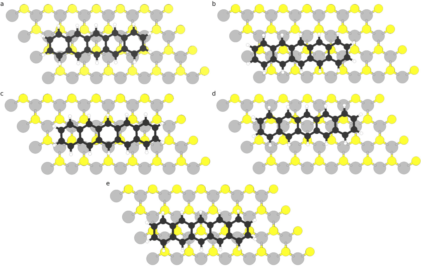 | ||
| Fig. 1 Ball and stick representation of the adsorption sites examined for the adsorption of pentacene molecule (horizontally oriented) on 2D monolayer TMD: (a) bridge-A, (b) bridge-B, (c) hollow, (d) top-TM, and (e) top-Ch. The adsorption sites were named based on the position of the central ring of the pentacene molecule. | ||
| System | PBE + vdW | PBE only | ||
|---|---|---|---|---|
| E ads (eV) | d (Å) | E ads (eV) | d (Å) | |
| PEN/MoS2 | −1.389 | 3.309 | −0.100 | 3.988 |
| PEN/MoSe2 | −1.425 | 3.400 | −0.101 | 4.020 |
| PEN/WS2 | −1.435 | 3.297 | −0.097 | 4.049 |
| PEN/WSe2 | −1.458 | 3.378 | −0.099 | 4.174 |
Adsorption energies (Eads) of pentacene/TMD systems were calculated as the difference between the total energy of the combined system (EPEN/TMD) and the total energies of the isolated systems (ErelaxTMD and Eiso-relaxPEN) in their relaxed geometries:
| Eads = EPEN/TMD − ErelaxTMD − Eiso-relaxPEN. | (1) |
From the results displayed in Table 1 we also observe that most of the adsorption energies are due to vdW interactions; when vdW interactions are switched off (see “PBE only” results in Table 1), the adsorption energies are reduced by one order of magnitude and the differences among the different TMD systems become even smaller. We also observe that vdW interactions bring the pentacene molecules closer to the substrate: PBE-only adsorption distances are at least 0.6 Å larger than those obtained including vdW corrections.
We can also examine the contributions to the adsorption energy from molecule–molecule and molecule–substrate interactions as well as from deformation of molecule and substrate (see ESI† for details of these calculations). As shown in Table 2, the largest contribution to the adsorption energy comes from the molecule–substrate interaction in contrast with the negligible contribution from molecule–molecule interaction. We also observe small values for the energy associated with the deformation of the molecules and the substrates. In fact, we did not observe any bending of the molecule under the adsorption process and the C–C bond length in pentacene changes by less than 0.1% in all four heterostructures when compared with isolated pentacene. For the TMDs, we observed small contractions (<0.1%) in the bond lengths between transition metal and chalcogen atoms, mostly in the region where the pentacene is adsorbed.
| PEN/MoS2 | PEN/MoSe2 | PEN/WS2 | PEN/WSe2 | |
|---|---|---|---|---|
| Molecule–molecule interaction | −0.004 | −0.003 | −0.004 | −0.003 |
| Molecule–substrate interaction | −1.402 | −1.423 | −1.340 | −1.452 |
| Molecule–deformation | 0.005 | −0.007 | −0.003 | −0.007 |
| Substrate–deformation | 0.012 | 0.008 | −0.088 | 0.004 |
In addition to the structural properties, we also investigated the electronic properties of pentacene/TMD heterostructures, considering single-layer pentacene on top-Ch adsorption sites for all the four TMDs. Fig. 2 displays the density of states (DOS) of pentacene/TMD heterostructures (considering the most favourable adsorption site, namely, top-Ch), clearly showing that the highest occupied molecular orbital (HOMO) of pentacene is located within the band gap of the 2D TMDs, closer to the valence band maximum (VBM) of the selenide systems, MoSe2 (Fig. 2(b)) and WSe2 (Fig. 2(d)) when compared to the sulfide systems, MoS2 (Fig. 2(a)) and WS2 (Fig. 2(c)). This helps to explain why the interaction between pentacene and the Se-system is stronger than that of pentacene and S-systems. The lowest unoccupied molecular orbital (LUMO) of pentacene is located above the conduction band minimum (CBM) of MoS2, MoSe2 and WS2, indicating that PEN/MoS2, PEN/MoSe2 and PEN/WS2 form staggered type-II heterostructures; however, pentacene's LUMO has lower energy than the CBM of WSe2 suggesting a type-I band alignment for PEN/WSe2 heterostructure. By examining the DOS of the isolated molecule and isolated monolayer WSe2 (see Fig. S1 of ESI†) we notice that the isolated systems have a type-II band alignment; however, molecule–molecule interactions present when the pentacene molecules are placed in a 7 × 4 supercell causes the HOMO and LUMO to shift by about 88 meV and 98 meV to lower energy, respectively, while molecule–substrate interaction causes an additional shift to lower energies of 209 meV for the HOMO and 194 meV for the LUMO (see Fig. S2 of ESI†), which leads to a transition from type-II to type-I alignment. Similar shifts were observed for the other three systems, as listed in Table S4 of the ESI.† Additional analysis of the electronic band structures of the PEN/TMD heterostructures in comparison with the band structures of monolayer TMDs (as displayed in Fig. S3 of ESI†) reveals that the adsorption of single layer pentacene molecules causes shifts of both CBM and VBM of the TMDs to higher energies. We found that the shifts in the CBM and VBM are 73 and 71 meV for MoS2, 62 and 64 meV for MoSe2, 62 and 67 meV for WS2, and 61 and 59 eV for WSe2. For WSe2, the shift of the CBM to higher energy also contributes to the type-II-to-type-I transition observed upon pentacene adsorption. We believe the shifts of pentacene HOMO and LUMO and TMDs VBM and CBM are due to the small charge transferred from pentacene to the TMD upon adsorption, as discussed in the next paragraphs.
 | ||
| Fig. 2 Total and partial density of states (DOS) of (a) PEN/MoS2, (b) PEN/MoSe2, (c) PEN/WS2 and (d) PEN/WSe2 heterostructures. The Fermi level of the heterostructure is indicated by a vertical dashed line. HOMO and LUMO of pentacene are highlighted in each plot. | ||
We have not considered the effect of spin–orbit coupling (SOC) in our calculations here. We do not expect significant changes in the adsorption energies and geometries, but for the electronic properties, SOC will cause splits in the topmost valence bands as well as in the lowest conduction bands of the TMDs, in particular for WS2 and WSe2. We have computed the shift of the VBM and CBM of the TMDs (see Table S5 of the ESI†), in order to infer if SOC would affect the type of band alignment observed here. For MoS2, the shifts of VBM and CBM due to SOC are less than 0.1 eV, while pentacene HOMO is located about 1 eV above the VBM of MoS2 and pentacene LUMO is located about 0.5 eV above the CBM of MoS2, which indicates that SOC will not change the type-II band alignment observed here. Type-II band alignment is also expected to be preserved for both MoSe2 and WS2, since SOC causes shifts of the MoSe2 and WS2 VBM by about 0.23 and 0.17 eV to higher energies, respectively, which is not enough to place VBM above pentacene HOMO (which is located about 0.4 eV above the VBM of MoSe2 and 0.8 eV above the VBM of WS2). As expected, WSe2 exhibits the largest shifts due to SOC: the VBM is shifted by about 0.33 eV to higher energies while the CBM is shifted by about 0.15 eV to lower energies. Since pentacene HOMO is located about 0.2 eV above WSe2 VBM and pentacene LUMO is located about 0.2 eV below WSe2 CBM, we expect that SOC will cause a larger hybridization between pentacene HOMO and WSe2 VBM as well as between pentacene LUMO and WSe2 CBM, facilitating charge transfer between these systems and potentially restoring the type-II band alignment.
Finally, we examine the charge transfer between pentacene molecules and the 2D TMD systems. Charge density difference between the heterostructure and isolated systems (Fig. 3) shows characteristics of a Pauli repulsion pillow effect for all the systems: the overlap between the electronic clouds of the molecule and the TMD causes the charge to be pushed back into the TMD and around the edges of the molecules (see also Fig. S4 in the ESI†)—red regions indicate accumulation of charge in the top chalcogen layer and around the edges of the molecules—leading to a depletion of charge (blue region) between the molecule and the 2D material. The push-back of charge into the top chalcogen layer has approximately the same amplitude in all four systems, as can be seen in Fig. 4(a), which displays the plane-averaged differential charge density (Δρ(z)) calculated by integrating the charge density within the basal x–y plane at a z point. By integrating Δρ(z) from bottom to z,  , which is shown in Fig. 4(b), we can estimate the charge transfer between the single layer pentacene molecules and the monolayer TMDs. We found that charge transferred from pentacene to the four TMDs are in the range of 0.011 to 0.013 e per supercell, which corresponds to 4–5 × 10⁻⁴ e per S/Se atom or 3.6–4.7 × 10¹¹ e cm−2. These values are significantly smaller than the charge transferred calculated between MXene Ti3C3 and Ti3C2F2 to 1T-MoS2 in ref. 42 (namely, 0.10 and 0.013 e per S atom, respectively) and between 2H-MoS2 and MoO3 in ref. 43 (namely, 2.0–4.5 × 10¹³ e cm−2), but in the same order of magnitude of the charge transferred calculated between H2O molecules and monolayer α-MoO3 in ref. 44 (namely, 0.02 e per H2O molecule). The reduction of the work function observed upon adsorption of the pentacene molecule, as seen in Table 3, originates mainly from the HOMO level of the molecule lying higher than the valence band edge of the TMDs, cf.Fig. 2. This is in line with the observation that the change in the work function of the Se-systems is smaller than that observed for S-systems; in addition, the push-back effect caused by the adsorption, which is similar in the S and Se compounds, contributes to the decrease of the work function.
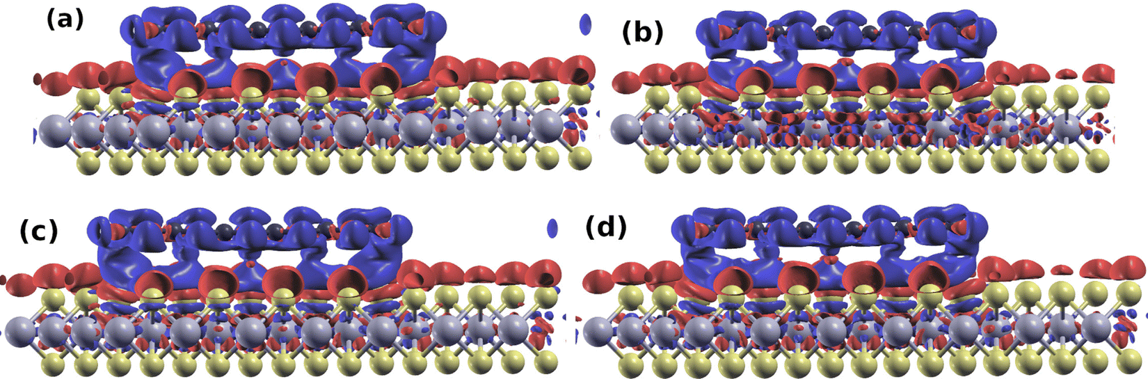 | ||
| Fig. 3 Charge density difference between the heterostructures ((a) PEN/MoS2, (b) PEN/MoSe2, (c) PEN/WS2 and (d) PEN/WSe2) and the isolated systems. Regions in blue and red represent depletion and accumulation of charge, respectively. Figure prepared using the XCrySDen software,45 with isovalues in the range of −0.0001 (blue) and +0.0001 (red) e bohr−3. | ||
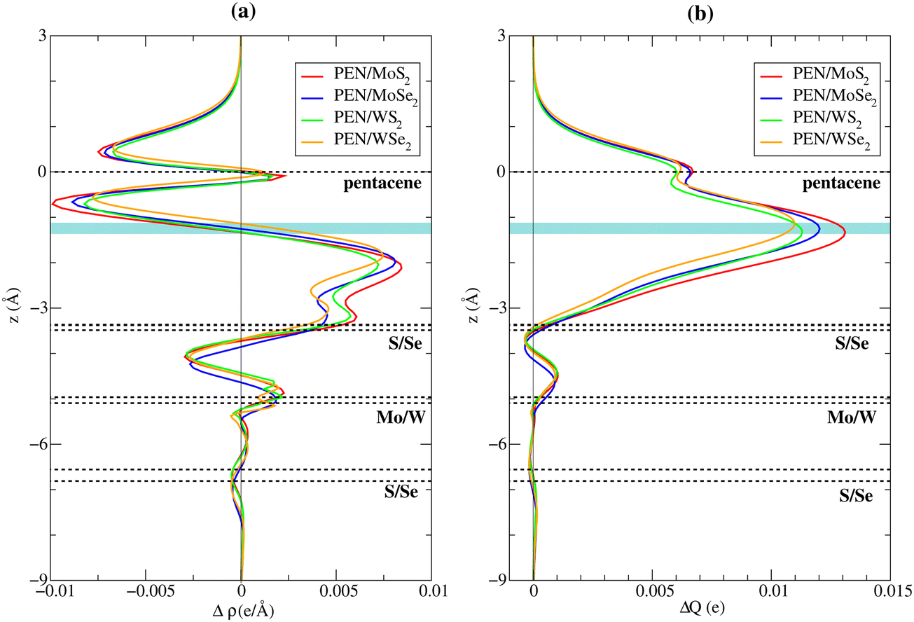 | ||
| Fig. 4 (a) Plane-averaged differential charge density (Δρ(z)) calculated by integrating the charge density within the basal x–y plane at a z point. (b) Charge transferred (ΔQ(z)) between pentacene and the TMDs at a z point, calculated by integrating Δρ(z) from bottom to z. Horizontal dashed lines show the positions of the pentacene molecule, and the top/bottom chalcogen layers and the transition-metal layer of the TMD monolayer. Cyan region indicates the position of the interface in the PEN/TMD heterostructures. | ||
| ϕ (TMD) (eV) | ϕ (PEN/TMD) (eV) | Δϕ = ϕ(TMD) − ϕ(PEN/TMD) (eV) | |
|---|---|---|---|
| MoS2 | 5.34 | 4.42 | 0.92 |
| MoSe2 | 4.46 | 4.21 | 0.25 |
| WS2 | 4.81 | 4.25 | 0.57 |
| WSe2 | 4.40 | 4.17 | 0.23 |
4 Conclusions
In summary, we have investigated the adsorption of single molecule pentacene on 2D monolayer TMDs (MoS2, MoSe2, WS2 and WSe2). Our results show that pentacene lies flat in all four TMDs, and interacts more strongly with MoSe2 and WSe2, which is reflected in a larger depletion of charge in the region between the molecule and the substrate. This also results in a smaller change in the work function caused by the adsorption of pentacene on MoSe2 and WSe2 when compared to MS2 and WS2, since the larger depletion of charge cancels out part of the push-back effect caused by the overlap between the electron densities of the molecule and the TMDs. Finally, we found that pentacene in a monolayer concentration forms type-II band alignment with MoS2, MoSe2 and WS2, since pentacene HOMO has higher energy than the VBM of these systems, while the CBM of the TMDs have lower energy than pentacene LUMO. For PEN/WSe2 we observed a type-I band alignment, since molecule–molecule and molecule–substrate interactions shift pentacene LUMO to lower energies, placing it below the CBM of WSe2. The discussion of the interaction between pentacene molecules and monolayer TMDs is valuable since such heterostructures show promising electronic properties for application in flexible, lightweight and thin photovoltaics.Author contributions
JM and PK conceived the project. EB and JM performed the calculations. JM supervised the project. All authors analysed and discussed the results and contributed to the writing of the manuscript. All authors have given approval to the final version of the manuscript.Data availability statement
The data that support the findings of this study are openly available at Keele Data Repository: https://doi.org/10.21252/j6dg-m071.Conflicts of interest
There are no conflicts to declare.Acknowledgements
This work was funded by the Deutsche Forschungsgemeinschaft (DFG, German Research Foundation), Projects 406901005 and 278162697 (SFB1242), and used the Cirrus UK National Tier-2 HPC Service at EPCC (https://www.cirrus.ac.uk) funded by the University of Edinburgh and EPSRC (EP/P020267/1).References
- S. Wi, H. Kim, M. Chen, H. Nam, L. J. Guo, E. Meyhofer and X. Liang, ACS Nano, 2014, 8, 5270–5281 CrossRef CAS PubMed.
- W. Du, P. Yu, J. Zhu, C. Li, H. Xu, J. Zou, C. Wu, Q. Wen, H. Ji, T. Liu, Y. Li, G. Zou, J. Wu and Z. M. Wang, Nanotechnology, 2020, 31, 225201 CrossRef CAS PubMed.
- E. Lee, Y. S. Yoon and D.-J. Kim, ACS Sens., 2018, 3, 2045–2060 CrossRef CAS PubMed.
- A. Perez, R. G. Amorim, C. E. P. Villegas and A. R. Rocha, Phys. Chem. Chem. Phys., 2020, 22, 27053–27059 RSC.
- A. O. A. Tanoh, N. Gauriot, G. Delport, J. Xiao, R. Pandya, J. Sung, J. Allardice, Z. Li, C. A. Williams, A. Baldwin, S. D. Stranks and A. Rao, ACS Nano, 2020, 14, 15374–15384 CrossRef CAS PubMed.
- C. Liu, H. Hong, Q. Wang, P. Liu, Y. Zuo, J. Liang, Y. Cheng, X. Zhou, J. Wang, Y. Zhao, J. Xiong, B. Xiang, J. Zhang and K. Liu, Nanoscale, 2019, 11, 17195–17200 RSC.
- S. Zhang, H. M. Hill, K. Moudgil, C. A. Richter, A. R. Hight Walker, S. Barlow, S. R. Marder, C. A. Hacker and S. J. Pookpanratana, Adv. Mater., 2018, 30, 1802991 CrossRef PubMed.
- T. Zou, H.-J. Kim, S. Kim, A. Liu, M.-Y. Choi, H. Jung, H. Zhu, I. You, Y. Reo, W.-J. Lee, Y.-S. Kim, C.-J. Kim and Y.-Y. Noh, Adv. Mater., 2023, 35, 2208934 CrossRef CAS PubMed.
- O. K. Le, V. Chihaia, V. Van On and D. N. Son, RSC Adv., 2021, 11, 8033–8041 RSC.
- S. Mouri, Y. Miyauchi and K. Matsuda, Nano Lett., 2013, 13, 5944–5948 CrossRef CAS PubMed.
- M. R. Habib, H. Li, Y. Kong, T. Liang, S. M. Obaidulla, S. Xie, S. Wang, X. Ma, H. Su and M. Xu, Nanoscale, 2018, 10, 16107–16115 RSC.
- S. F. Nelson, Y.-Y. Lin, D. J. Gundlach and T. N. Jackson, Appl. Phys. Lett., 1998, 72, 1854–1856 CrossRef CAS.
- R. He, N. G. Tassi, G. B. Blanchet and A. Pinczuk, Appl. Phys. Lett., 2010, 96, 263303 CrossRef.
- S. S. Kim, Y. S. Choi, K. Kim, J. H. Kim and S. Im, Appl. Phys. Lett., 2003, 82, 639–641 CrossRef CAS.
- A. Maliakal, K. Raghavachari, H. Katz, E. Chandross and T. Siegrist, Chem. Mater., 2004, 16, 4980–4986 CrossRef CAS.
- S. Bettis Homan, V. K. Sangwan, I. Balla, H. Bergeron, E. A. Weiss and M. C. Hersam, Nano Lett., 2017, 17, 164–169 CrossRef CAS PubMed.
- N. Shen and G. Tao, Adv. Mater. Interfaces, 2017, 4, 1601083 CrossRef.
- S. R. Kachel, P.-M. Dombrowski, T. Breuer, J. M. Gottfried and G. Witte, Chem. Sci., 2021, 12, 2575–2585 RSC.
- M. R. Habib, W. Wang, A. Khan, Y. Khan, S. M. Obaidulla, X. Pi and M. Xu, Adv. Theory Simul., 2020, 3, 2000045 CrossRef CAS.
- W. Kohn and L. J. Sham, Phys. Rev., 1965, 140, A1133–A1138 CrossRef.
- P. Giannozzi, S. Baroni, N. Bonini, M. Calandra, R. Car, C. Cavazzoni, D. Ceresoli, G. L. Chiarotti, M. Cococcioni and I. Dabo, et al. , J. Phys.: Condens. Matter, 2009, 21, 395502 CrossRef PubMed.
- P. Giannozzi, O. Andreussi, T. Brumme, O. Bunau, M. B. Nardelli, M. Calandra, R. Car, C. Cavazzoni, D. Ceresoli and M. Cococcioni, et al. , J. Phys.: Condens. Matter, 2017, 29, 465901 CrossRef CAS PubMed.
- J. P. Perdew, K. Burke and M. Ernzerhof, Phys. Rev. Lett., 1996, 77, 3865 CrossRef CAS PubMed.
- S. Grimme, J. Antony, S. Ehrlich and H. Krieg, J. Chem. Phys., 2010, 132, 154104 CrossRef PubMed.
- L. Cabral, F. P. Sabino, M. P. Lima, G. E. Marques, V. Lopez-Richard and J. L. F. Da Silva, J. Phys. Chem. C, 2018, 122, 18895–18901 CrossRef CAS.
- K. Toyoda, I. Hamada, K. Lee, S. Yanagisawa and Y. Morikawa, J. Phys. Chem. C, 2011, 115, 5767–5772 CrossRef CAS.
- P. Ji, D. Dettmann, Y.-H. Liu, G. Berti, N. Preetha Genesh, D. Cui, O. MacLean, D. F. Perepichka, L. Chi and F. Rosei, ACS Nano, 2022, 16, 6506–6514 CrossRef CAS PubMed.
- S. Kamalakannan, M. Prakash, M. M. Al- Mogren, G. Chambaud and M. Hochlaf, J. Phys. Chem. C, 2019, 123, 15087–15098 CrossRef CAS.
- M. J. van Setten, D. Xenioti, M. Alouani, F. Evers and R. Korytár, J. Phys. Chem. C, 2019, 123, 8902–8907 CrossRef CAS.
- W. Hao, Y. Wang, H. Zhao, J. Zhu and S. Li, Phys. Chem. Chem. Phys., 2020, 22, 13802–13807 RSC.
- F. Eisenhut, J. Krüger, D. Skidin, S. Nikipar, J. M. Alonso, E. Guitián, D. Pérez, D. A. Ryndyk, D. Peña, F. Moresco and G. Cuniberti, Nanoscale, 2018, 10, 12582–12587 RSC.
- B. P. Klein, J. M. Morbec, M. Franke, K. K. Greulich, M. Sachs, S. Parhizkar, F. C. Bocquet, M. Schmid, S. J. Hall, R. J. Maurer, B. Meyer, R. Tonner, C. Kumpf, P. Kratzer and J. M. Gottfried, J. Phys. Chem. C, 2019, 123, 29219–29230 CrossRef CAS.
- S. R. Kachel, B. P. Klein, J. M. Morbec, M. Schöniger, M. Hutter, M. Schmid, P. Kratzer, B. Meyer, R. Tonner and J. M. Gottfried, J. Phys. Chem. C, 2020, 124, 8257–8268 CrossRef CAS.
- P. E. Blöchl, Phys. Rev. B: Condens. Matter Mater. Phys., 1994, 50, 17953–17979 CrossRef PubMed.
- Quantum ESPRESSO pslibrary, https://pseudopotentials.quantum-espresso.org/legacy_tables/ps-library.
- T. Sohier, M. Calandra and F. Mauri, Phys. Rev. B, 2017, 96, 075448 CrossRef.
- H. J. Monkhorst and J. D. Pack, Phys. Rev. B: Solid State, 1976, 13, 5188–5192 CrossRef.
- C. M. O. Bastos, R. Besse, J. L. F. Da Silva and G. M. Sipahi, Phys. Rev. Mater., 2019, 3, 044002 CrossRef CAS.
- K.-A. N. Duerloo, Y. Li and E. J. Reed, Nat. Commun., 2014, 5, 4214 CrossRef CAS PubMed.
- J. Krumland and C. Cocchi, Electron. Struct., 2021, 3, 044003 CrossRef CAS.
- S. S. Batsanov, Inorg. Mater., 2001, 37, 871–885 CrossRef CAS.
- Q. Guan, H. Yan and Y. Cai, Adv. Mater. Interfaces, 2022, 9, 2101838 CrossRef CAS.
- Z. Gao, Z. Zhou and D. Tománek, ACS Nano, 2019, 13, 5103–5111 CrossRef CAS PubMed.
- C. Huan, P. Wang, B. He, Y. Cai and Q. Ke, J. Mater. Chem. C, 2022, 10, 1839–1849 RSC.
- A. Kokalj, J. Mol. Graphics Modell., 1999, 17, 176–179 CrossRef CAS PubMed.
Footnote |
| † Electronic supplementary information (ESI) available. See DOI: https://doi.org/10.1039/d3cp01895d |
| This journal is © the Owner Societies 2023 |