
 Open Access Article
 This Open Access Article is licensed under a Creative Commons Attribution-Non Commercial 3.0 Unported Licence
Second harmonic generation from aluminum plasmonic nanocavities: from scanning to imaging†
Tchiya
Zar
 a,
Alon
Krause
a,
Omer
Shavit
ab,
Hannah
Aharon
a,
Racheli
Ron
a,
Martin
Oheim
b and
Adi
Salomon
*ab
a,
Alon
Krause
a,
Omer
Shavit
ab,
Hannah
Aharon
a,
Racheli
Ron
a,
Martin
Oheim
b and
Adi
Salomon
*ab
aDepartment of Chemistry, BINA Nano Center for advanced materials, Bar-Ilan University, Ramat-Gan, Israel. E-mail: adi.salomon@biu.ac.il
bUniversité Paris Cité, CNRS, Saints Pères Paris Institute for the Neurosciences, F-75006 Paris, France
First published on 29th June 2023
Abstract
Metamaterials and plasmonic structures made from aluminum (Al) have attracted significant interest due to their low cost, long-term stability, and the relative abundance of aluminum compared to the rare metals. Also, aluminum displays distinct dielectric properties allowing for the excitation of surface plasmons in the ultraviolet region with minimal non-radiative losses. Despite these clear advantages, most of the research has been focused on either gold or silver, probably due to difficulties in forming smooth thin films of aluminum. In the present work, we detect and characterize second harmonic generation (SHG) in the optical regime, emanating from triangular hole arrays milled into thin aluminum films in reflection mode, at normal incidence. We report intense nonlinear responses, year-long stability, and overall superior performances with respect to gold. The robustness of the Al structures and high reproducibility of the measured SHG responses allowed us to investigate changes in the directional emission upon tiny modifications in the structure's symmetry. We also demonstrate large-field instantaneous SHG imaging over areas containing several hole arrays using a recent, non-linear single-spinning disk microscope. Such high spatio-temporal resolution imaging has important applications, e.g., when studying chemical transformations occurring at electrode surfaces during charging and discharging cycles, as well as ageing.
Introduction
Non-linear optical processes, including second harmonic generation (SHG), are highly sensitive to surface modifications, such as asymmetry, defects, dipole orientation, changes in the local chemical environment, or the refractive index,1–7 and they are used for the readout of surface properties and modification in many fields.8–15SHG is a process in which two photons at the fundamental frequency (ω) combine to form one photon at the double frequency (2ω). As a second order process, SHG responses from materials with inversion symmetry such as metals are negligible.16 Although, SHG signals are inherently weak, the enhancement of the electromagnetic (EM) field at 2ω or/and at ω can improve significantly the signal intensity in proportion to (|E(ω)2|·|E(2ω)|)2.1,3,17–19 One way to enhance SHG responses is coupling to plasmonic modes.20,21 Surface plasmons (SPs) are coherent oscillations of the metal's free electrons19,22–24 and due to their deep confinement, they provide the required field flux densities. Enhanced nonlinear optical responses have been demonstrated on various thin-layer metals, and for both nano-particles and nano-cavities milled in thin films.1,2,17,18,25–27
Despite their optical losses due to interband transitions (for Au at ∼520 nm),28–34 Ag or Au surfaces are often used for plasmonic devices. Aluminum (Al), on the other hand, has no transition at the UV-visible and almost perfectly fits to the Drude free electron model, with a narrow interband transition in the near-infrared.17,28,33,35 Its high bulk-plasmon energy of about 15 eV36 is an advantage for plasmonic devices, which potentially can operate in the UV.32,36–43 In addition, the value of the low work function of Al is suitable for electron injection and thus for opto-electronic devices and for complementary metal-oxide-semiconductor (CMOS) applications.44 Indeed, Al has been recognized as a metal of choice for expanding the functioning photonic devices into the visible-UV range.28,45–50 Yet, unfortunately, preparing smooth aluminum surfaces is quite challenging, due to high surface mobility of its atoms, leading to relatively large grain size, and producing defects at the nano scale.39
Nevertheless, SHG responses from aluminum well-defined plasmonic nano-structures have been successfully demonstrated,1,17,51–53 with conversion efficiency of about ηSHG ∼ 10−12 have been reported,16 comparable to other well-defined plasmonic nano-structures from gold or silver.18,54 Of note, relatively high conversion efficiency of ηSHG ∼ 10−11 was observed from silver 3D metallic networks.55 On the other hand, relatively few imaging studies reading out SHG from plasmonic structures in general have been reported,56 probably due to low conversion efficiency.
In this paper we study SHG response emanating from triangular hexagonal hole arrays milled in thin aluminum film (∼200 nm), excited at normal incidence at reflection mode. We report high nonlinear responses from samples that remained stable over years, thus showing an overall superior performance with respect to other plasmonic surfaces. The robustness of our structures and the high reproducibility of the measured signal allowed us to investigate changes in directional emissions upon small modification of the array periodicity. Finally, the high nonlinear efficiency lends itself in a natural way to demonstrate SHG imaging over large surface areas, containing several hole arrays structures, by using a new non-linear single spinning disk microscope.57 Our high spatio-temporal resolution SHG imaging scanned an area of 200 μm by 200 μm within less than 480 ms, at 146 nm per pixel. We believe the high efficiency together with our SHG imaging technique can pave the way for studying dynamic chemical transformations occurring at metallic electrode surfaces.
Results and discussion
In order to match the plasmonic modes to resonate with both the fundamental beam and the SH wavelengths, we used a triangular hexagonal hole array with different periodicities, P, that we varied from 305 nm to 505 nm. All arrays have an identical sub-unit of a triangular cavity with a side length of ∼225 nm and a base of ∼215 nm. All samples were fabricated using focus ion beam (FIB) milling in a flat 200 nm Al film, and all were coated by a ∼150 nm thick PVA film. In order to obtain smooth aluminum film on a fused silica substrate, the substrates have been carefully cleaned and special care was taken upon film deposition as is described in the experimental part. Film deposition resulted in a smooth film with average grain sizes of about 30 nm, allowing for accurate FIB milling of the triangular holes (see Fig. 1a). An example of the linear response of a hexagonal array with P = 405 nm is shown in Fig. 1b. Two main peaks are observed, one in the near–IR and the other in the visible regime.53 These plasmonic modes overlap with both the fundamental (ω) and the SH wavelength (2ω) at 940 nm and at 470 nm, respectively. The observed minimum at ∼830 nm is due to the intra-band transition of Al.58,59 The linear optical responses of all studied triangular arrays are summarized in Fig. 1c, which displays the dispersion relation of the measured plasmonic peaks with respect to the momentum (∼1/P), the full width at half maximum (FWHM) are indicated on the graph. The graph shows also a good agreement with the extraordinary transmission observed light micrographs shown in Fig. S1 (ESI†).60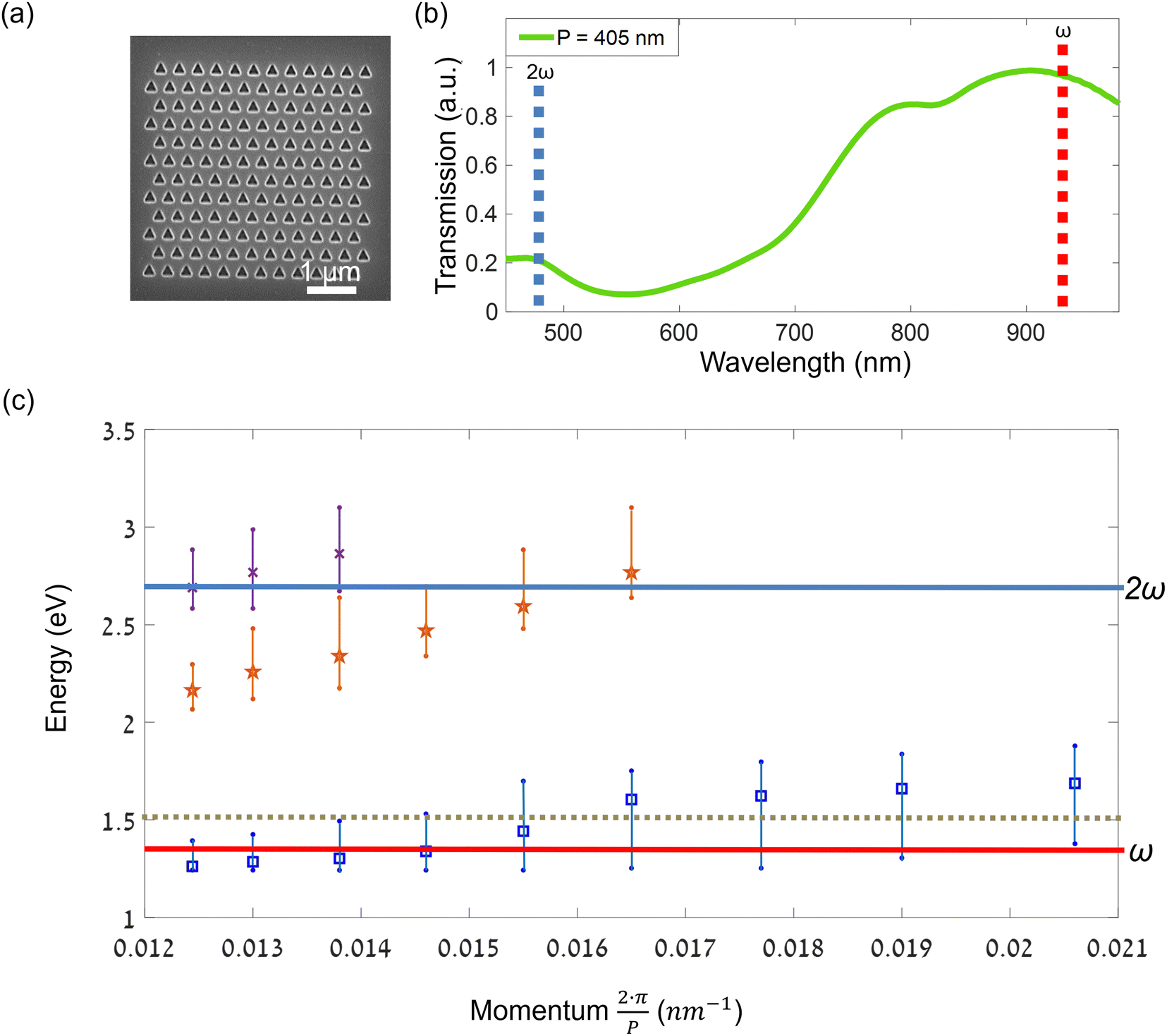 | ||
| Fig. 1 Linear optical measurements. (a) Scanning electron microscope (SEM) image of a typical Al triangular hole-array. (b) Linear transmission spectrum of an array with periodicity P = 405 nm, shows plasmonic modes at ω = 940 nm and at 2ω = 470 nm (marked by red and blue dashed bands). (c) Dispersion relation of a set of arrays with Ps of 305 nm to 505 nm with their FWHM (momentum of 2π/P). The dash line indicates the interband transition in aluminum and the solid lines are guides lines for the position of both fundamental wavelength and SH frequencies. See also Fig. S1 (ESI†) for transmission spectra and images. | ||
In order to measure SHG, we excited the plasmonic structures at 940 nm and normal incidence and collected the response in reflection mode through a NA-0.5 air objective after appropriate filtering, Fig. 2a. To make sure that we collected SH photons, we also measured the SH spectrum (see below). A typical result of a SHG scan of triangular array with P = 380 nm is shown on Fig. 2b. We note that the non-linear response was quite uniform over the array and decayed at the array boundaries. The response of the array was about 6 times higher compared to the surrounding smooth Al surface (see Fig. S2, ESI†). As expected, SH intensities showed a quadratic power dependence (Fig. 2c). Of note, our aluminum plasmonic structures can sustain an average laser power of 10 mW.
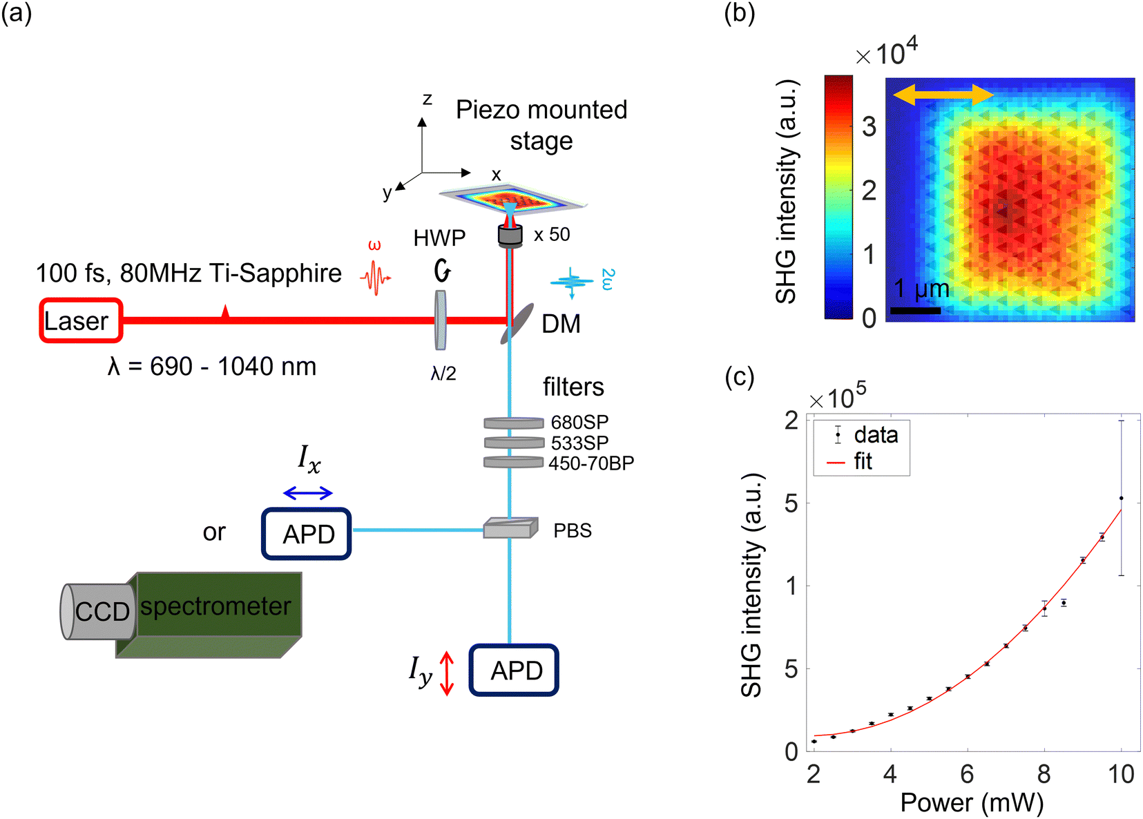 | ||
| Fig. 2 SHG detection and typical results. (a) Schematic illustration of the SHG setup. The 940 nm beam from a Ti:sapphire laser is expanded to fill the back aperture of a x50/NA0.5 air objective. The sample is piezo-scanned though the resulting focal spot. The excitation polarization is controlled by a motorized rotatable half-wave plate (HWP). The dichroic mirror (DM) separate the reflected fundamental excitation beam from the SHG signal. Short-pass (SP) and band-pass (BP) filters with cut-off at 500 nm are placed to reject parasite photons. The reflected SH response is directed via a polarized beam splitter (PBS) onto two orthogonal avalanched photodiodes (APDs) operating in photon counting mode. Alternatively, the generated signal can be detected on a spectrograph coupled to charge-coupled device (CCD) (for more details see Experimental section at ESI†). (b) Typical SHG response from a triangular hole-array (P = 380 nm) over a scanned area of 5 × 5 μm2, λ = 940 nm and laser power of 5 mW. (c) SHG intensity vs. laser power (dots) and square power law (red), respectively. See also Fig. S2 (ESI†). | ||
Next, we compared the resulting SHG intensities emanating from arrays with different periodicities P at two orthogonal polarizations of the excitation incident beam. For each array, we acquired SHG responses for two orthogonal polarizations, as shows in Fig. 3a. Although higher responses were observed for arrays with periodicities P between 380 and 480 nm which resonate better with both the fundamental (ω) and the SH (2ω) wavelengths (see Fig. 1c), the response modulations were not high enough to draw firm conclusions.
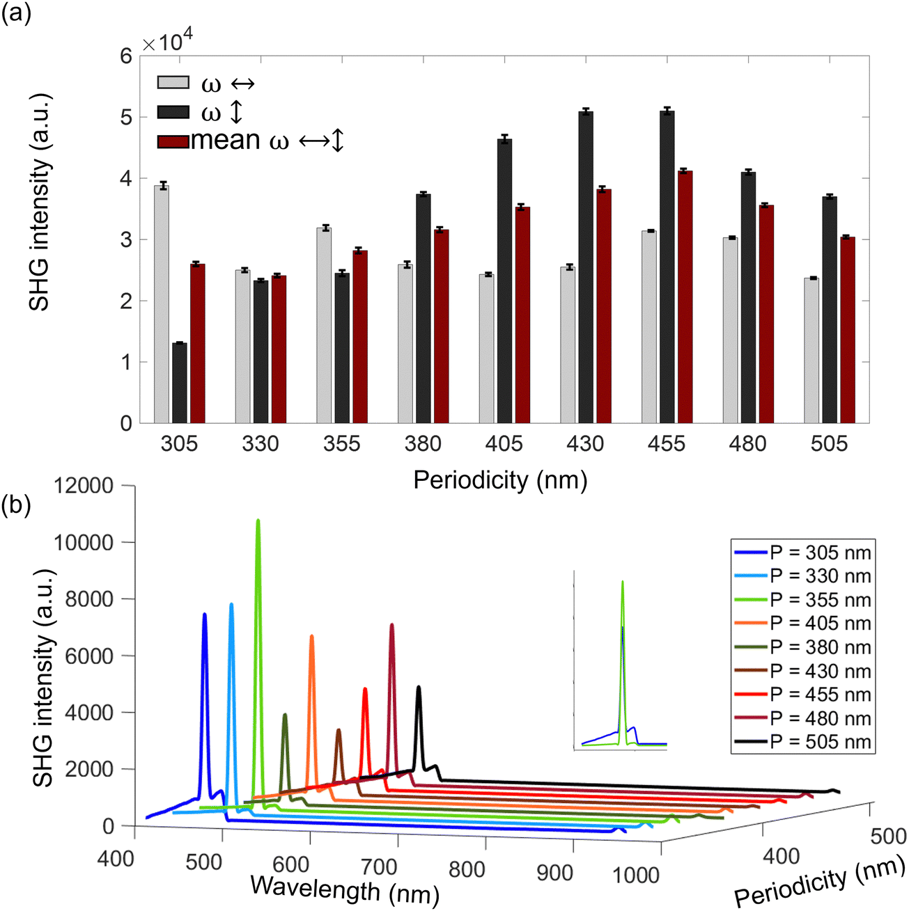 | ||
| Fig. 3 Dependence of SHG on array periodicity and excitation polarization. (a) SHG intensities responses from a set of triangular hole-arrays with different periodicities under two orthogonal polarizations of the incoming fundamental beam, 0° (ω ↔, light gray), 90° (ω ↕, dark gray) and their average (brown). (b) Reflection spectra 0° excitation polarization. All spectra show a clear peak at 470 nm, with some shoulder at ∼500 nm for some array. The fundamental wavelength at 940 nm is seen as well at the far end of the spectrum. Inset: Spectra for P = 305 and P = 355 nm displayed higher and broader spectrum for P of 305 nm, probably due to fluorescence. | ||
SHG spectra of those arrays are shown in Fig. 3b. The sharp decrease near 500 nm is due to the BP filter (see Fig. 2a for set-up description). A particular case is the spectrum of the array with P = 305 nm (blue, see inset image), showing signal that was not only due to SH process, but also due to photoluminescence, which explains the relatively ‘high’ response observed on Fig. 3a at 305 nm for 0° polarization (ω ↔). We think that, especially at this polarization, the localized EM field, leads to other multiphoton processes as well, among them photoluminescence.13
In order to obtain information regarding the second order susceptibility, χ(2), which reflects the material symmetry, we measured SHG upon full excitation polarization scans.61 In these experiments, the excitation polarization is modified by rotating the motorized HWP, and SHG is simultaneity detected by two APDs, on orthogonal arms of the PBS (see Fig. 2a and 4a). Since only the excitation polarization is modified but the analyzers are fixed, we expect quadrupole polar plots for our structures having a three-fold symmetry.61,62 Indeed, SHG emanating from a triangular hole-array having P = 380 nm and collected by two orthogonal APDs showed a clear quadruple symmetry. As a corollary, this result also indicates the stability of the plasmonic system as the response was stable over the min required for scanning the entire hole array (note that the SHG responses at the starting/end points are virtually identical, and the “cloverleaf’ figures are perfectly closed).3 In addition, we show on Fig. S3 (ESI†) the overlay of two measurements taken from the same array more than three years apart that clearly gave a similar result, attesting the long-term stability.
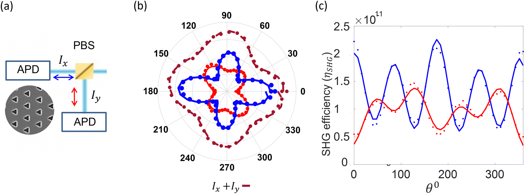 | ||
| Fig. 4 Rotational SHG for triangular hole array with P = 380 nm. (a) Illustration of SHG detection in two orthogonal channels (Ix and Iy). The diameter of the fundamental beam impinging on the array was about 2 μm. (b) Polar plots of the excitation-polarization dependent SHG response for the two orthogonal channels (Ix blue, Iy red), and their sum (Ix + Iy, brown) shows the χ(2) tensor. (c) Cartesian representation of the same data as shown in (b), with scale of conversion efficiency (ηSHG), see Table S1 at ESI.† | ||
Next we measured similar SHG-intensity polar plots from structures having different periodicities, Fig. 5. Although, in principle, all arrays have the same lattice symmetry and are composed of the same triangular cavities, their SHG emission patterns differed, showing a smooth variation with P. Fig. 5a displays the intensity ratio (90°/0°) of the combined SHG (Ix + Iy, brown) response as a function of P. The dominant SHG dipole emission is reversed, as is seen by the calculated ratio, which increase from ∼0.5 to ∼2 for larger periodicities. The shift of the dipole is clearly appreciated as well on the polar plots measured for all the arrays (Fig. 5a, top row). Fig. 5b draws a cartesian representation for three selected arrays with different P: where the SHG dipole was dominantly in x direction (P = 305 nm), in y direction (P = 455 nm), and an intermediate mode (P = 380 nm). The same data are identified on Fig. 5a by blue circles having the same line style (for further information see Fig. S4, ESI†).
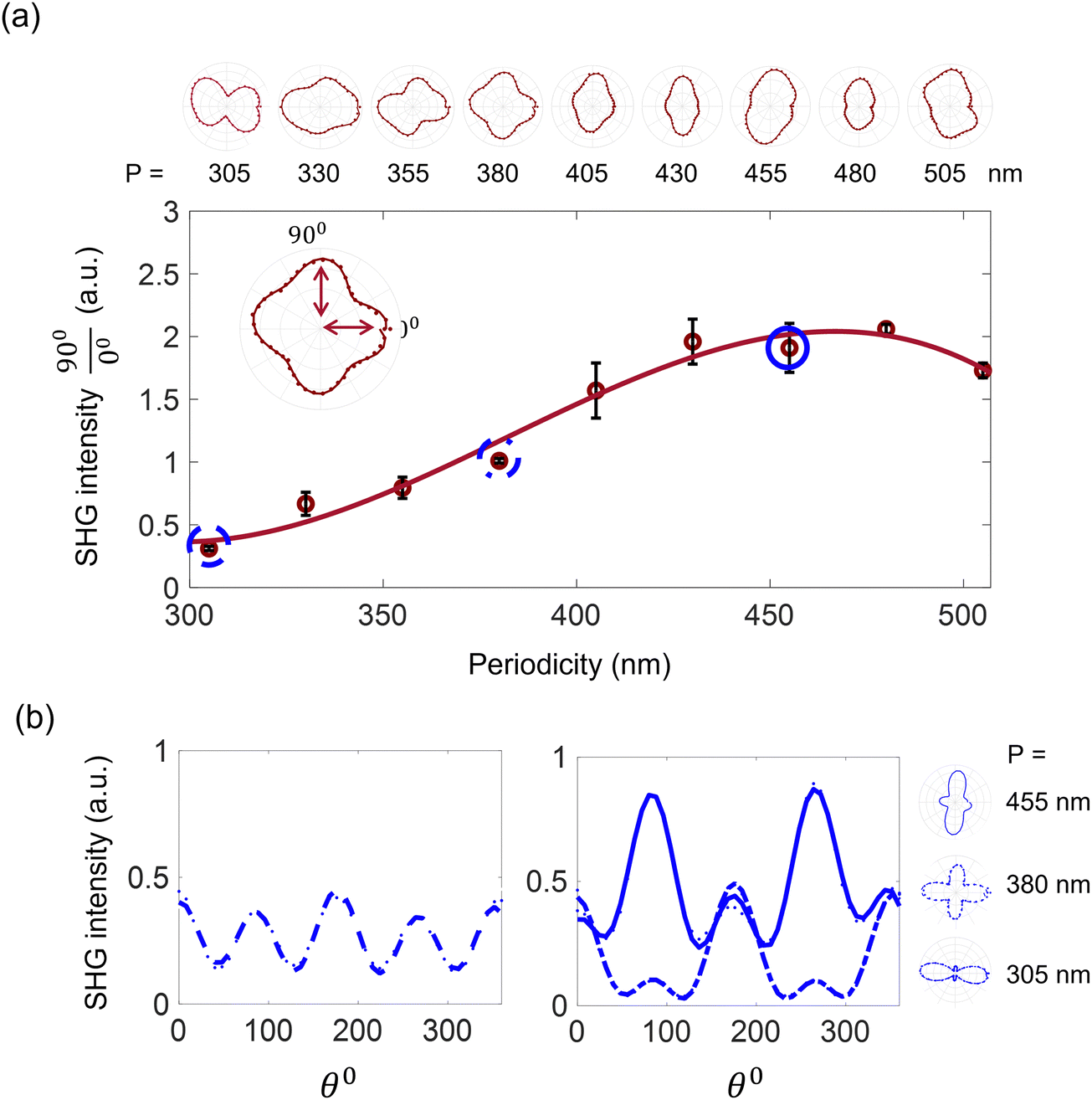 | ||
| Fig. 5 Excitation polarization dependence of SHG. (a) Measured SHG-intensity ratio for two orthogonal excitation polarizations as shown on the polar plot angles, 90° and 0° for a set of hexagonal arrays. Top: The correspondence polar plots SH emissions (Ix + Iy) for all the studied arrays. Inset: Indication of 90° and 0° angles. (b) A cartesian presentation of emission polar plots collected at x direction for P = 380 nm (left), and P = 305 nm, 455 nm (right) and their respective polar representation, right. Although all structures are made from the same sub-unit (triangular cavity), there is a clear and gradual change in the SHG emission pattern. | ||
What is the reason for this unexpected behavior? We excluded the role of the fundamental wavelength, by repeating our measurements at different wavelengths (Fig. S5, ESI†). We next considered the spatial arrangement of the triangle nano-cavities vs. bulk Al surface, which impacts on the spatial distribution of the plasmonic modes. As a matter of fact, previous research has shown that the plasmonic modes of triangle nanocavities concentrated on the triangle's sides, and they can propagate onto the metal conductive surface, allowing for a hybridization between close by nanocavities to form a new eigenmode onto the flat surface, whose frequency is dependent on the distance between them.16,18,63 Thus, depending on the proximity between nearby units (cavities), we expect the spatial localization of the enhanced EM field to be changed.
This is illustrated in Fig. 6, which shows the observed dipolar and quadropolar SHG responses as polar plots, along with the expected location of surface plasmon hotspots. At low periodicity (P = 305 nm), the proximity between the nanocavities makes it difficult for the plasmon to propagate on the metal surface, so the plasmon modes will be located on the triangle sides (Fig. 6 left). That can also explain the anomaly we saw at the spectra in Fig. 3b, of more parasitic photons from P = 305 nm compared to the other spectra.
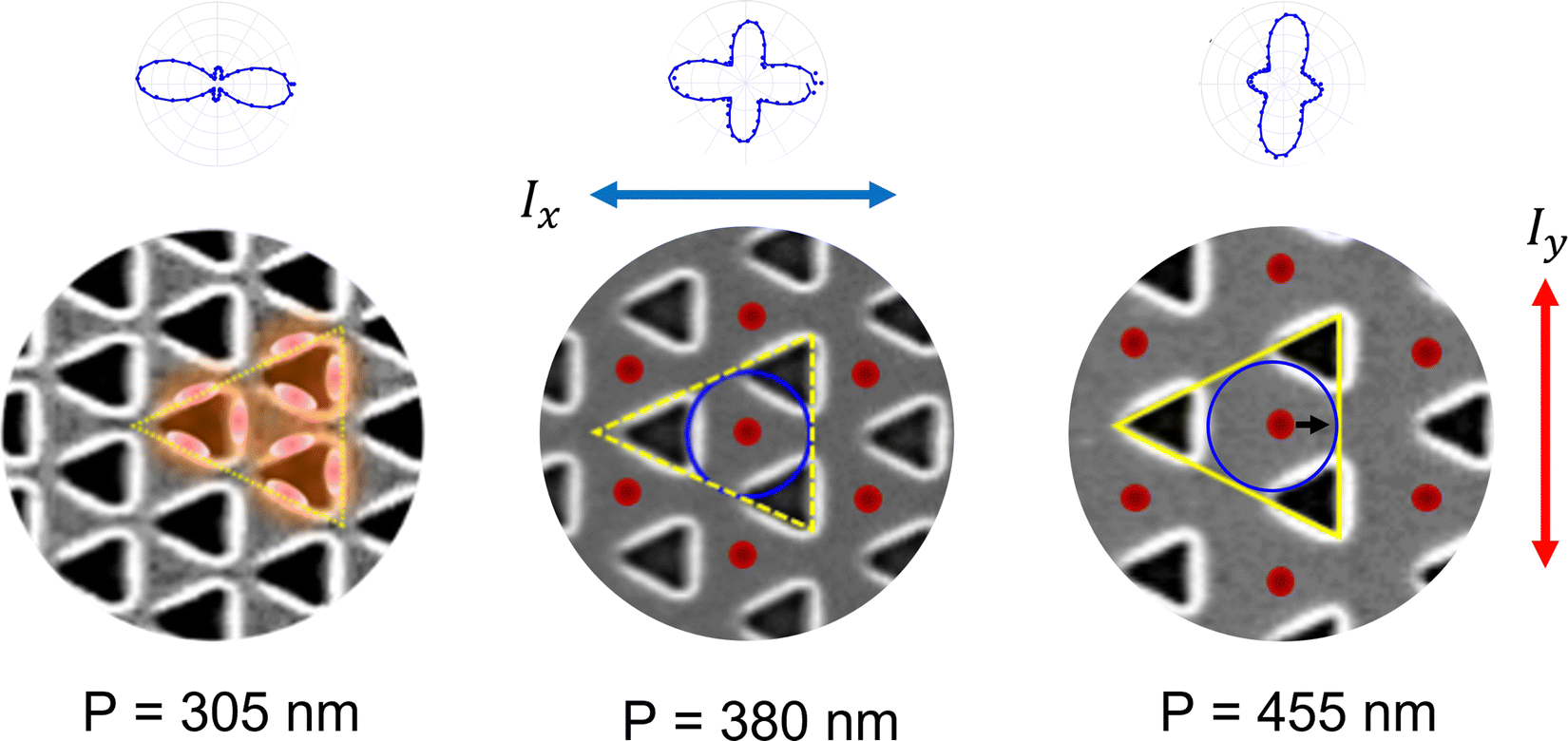 | ||
| Fig. 6 Heuristic explanation of the observed shift in the dipole axis. Top: Measured polar plots collected at x direction (blue). Down: Spatial distributions of the plasmonic modes (red lobs/circles) in between three adjacent cavities (yellow polygons), for three arrays with periodicities of 305, 380 and 455 nm. The blue circles are blocked in the yellow triangles. The little black arrow indicates changes in the spatial distribution of the EM field. | ||
When the periodicity increases, the distance between two cavities is such that plasmonic modes propagate onto the surface between the cavities and form hot spots located in between the nanocavities (Fig. 6, middle and right).64,65 Geometrical factors also shape the precise location: for P = 380 nm, the plasmon mode is located in the middle of the circle (blue) inscribed in the isosceles triangle (dashed yellow), meaning at the center between three adjacent nanocavities. On the other hand, for P = 455 nm, the symmetry is broken and the circle is no longer in the middle but slightly shifted to the triangle base as the yellow triangle grows. This leads us to believe that the plasmonic modes of the triangular nanocavities at the base of the yellow triangle become more dominant as do the plasmonic modes located nearer to them (black arrow).65 That can give a plausible explanation, based on theoretical calculations from ref. 65, to the shape change in the polar plots, from dominantly x direction (triangle sides) to y direction (triangle base).
As mentioned earlier, the origin of the relatively high SHG responses in these plasmonic structures lies in breaking the symmetry by the sub-wavelength triangular cavities. The enhancement is attributed to lack of inversion symmetry in the triangular cavities and their relatively sharp corners. In addition, the plasmonic eigenmodes of those hexagonal arrays overlap both with fundamental beam and the second harmonic wavelengths, ensuring that incident light and the generated second harmonic light efficiently confined within the plasmonic structure. The PVA on top of the metallic film, help to achieve the resonance matching as well. Yet, the polarization-dependent SHG measurements (see Fig. 5 and 6) indicate the possibility for involvement of another mechanism related to the formation of hotspots on the flat surface, between the cavities. Consequently, the plasmonic modes excited at the triangular cavities side lengths at the fundamental frequency propagate onto the surface and combine to create hotspots at the SHG frequency.18 The choice of aluminum hence, contribute to formation of hot-spots between the cavities, as aluminum posses less ohmic losses compared to other common used metals in plasmonic (silver and gold).
The efficiency of those triangular plasmonic cavities milled in aluminum has been measured and calculated to be approximately ∼2 × 10⁻¹¹ (see Tables S1–S3, ESI†). Fig. 7 presents a comparison between plasmonic structures milled in aluminum and those milled in gold, having the same geometrical parameters. Despite using a higher laser power of 8 mW for gold compared to 5 mW for aluminum, the SHG intensities are found to be higher for the aluminum plasmonic structures. Both aluminum and gold exhibit plasmonic properties that can enhance the local electromagnetic field. Yet, as is mentioned above, due to interband transition in gold it has less plasmonic response at this optical wavelengths region, making it less efficient for SHG applications within this wavelength range. Aluminum, on the other hand, support plasmonic excitation in the ultraviolet and visible regions, making it superior for SHG at this specific wavelength ranges. Furthermore, aluminum has relatively low absorption, i.e., less optical losses compared to gold at this wavelength range, leading to longer propagation length66 of the plasmonic modes and thus contributing to more efficient light-matter interaction and SHG enhancement. The comparison between gold and aluminum is summarized in Fig. 7b, illustrating that indeed aluminum exhibits a higher efficiency by a factor of up to 3.5. Yet, since the SHG emanating in those plasmonic structures only from the interface, their susceptibility is still low compared to commercial nonlinear materials, which are noncentrosymmetric by nature, as is summarized in the table Fig. 7c.
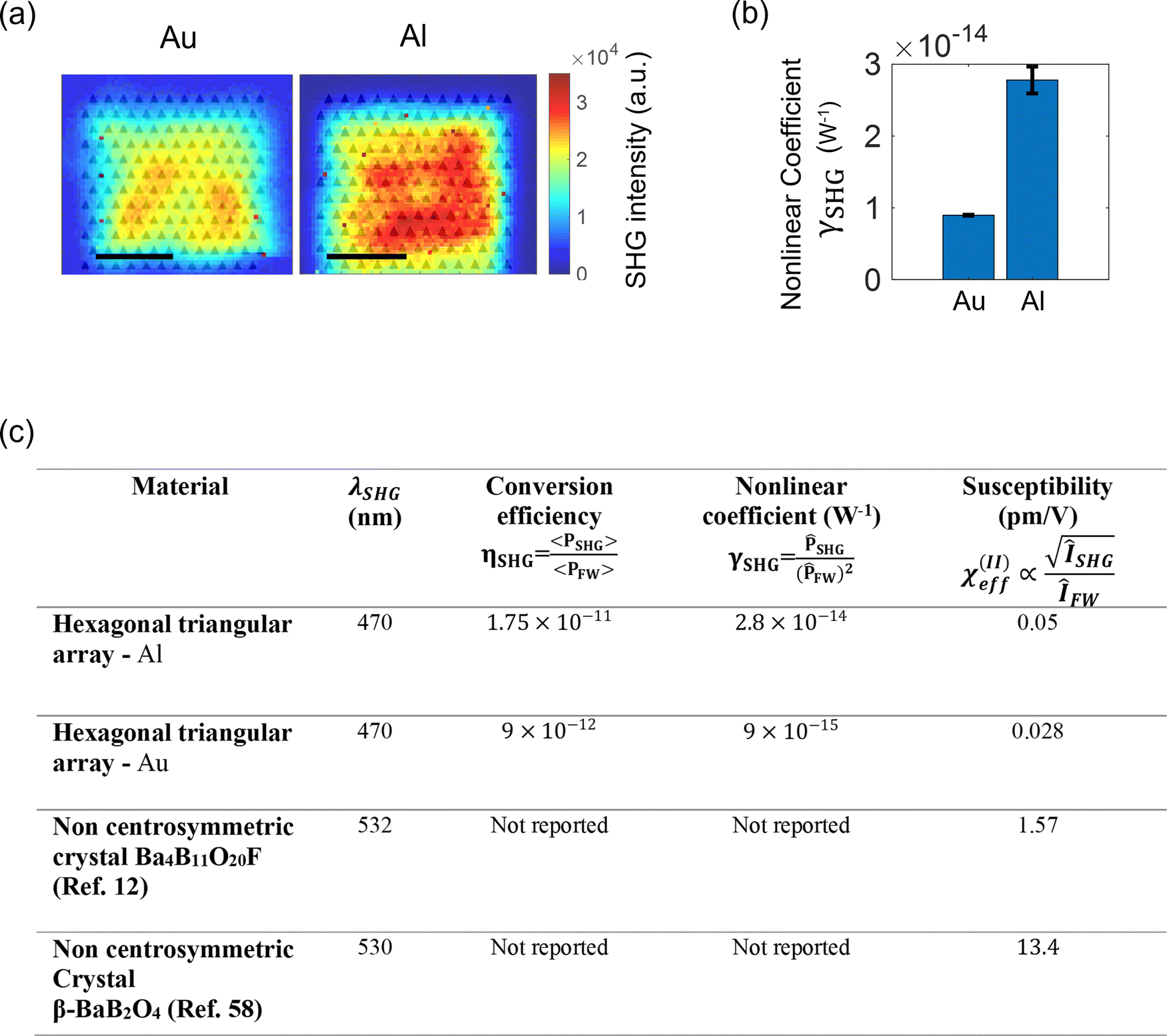 | ||
| Fig. 7 SHG responses of triangular hexagonal hole arrays (P = 405 nm) milled in Au and Al and covered by PVA. (a) Scanning of SHG responses, fused with the SEM images for clarity. Scale bars are 2 μm. The laser power was 8 mW for Au and 5 mW for Al. (b) Histogram of the calculated nonlinear coefficient, showing that for the same plasmonic structure, Al has higher nonlinear response. (c) A table which summaries the nonlinear properties of the reported measured samples in this study and their comparison with other bulk materials such as Ba4B11O20F (see ref. 12), and BBO (see ref. 58). | ||
The observed dependencies of the SHG response on both the polarization angle and on tiny changes in the surface geometry make our technique potentially attractive for monitoring dynamic alterations occurring on metallic surfaces. These can be as a consequence of surface chemical reactions, e.g., electrode surface modifications in response to charge/discharge cycles of batteries and other examples.3,53 However, in such applications, the commonly used scanning-stage geometry (that we also employed in our previous experiments) is too slow, because macroscopic surface areas must be monitored. In as much as SHG relies on high instantaneous photon intensities in the focus of a single fs-pulsed near-IR beam, the only way to speed up acquisitions in such a single-spot geometry is to shorten the pixel dwell time while compensating the signal loss by cranking up the laser power, at the risk of damaging the sample.
Interestingly, a very similar problem is encountered when imaging large tissue volumes in biological 2-photon microscopy67 at high spatio-temporal resolution. One solution that has been proposed57 to increase the photon budget while keeping non-linear damage low is a new rapid multi-spot scanning scheme, in which a rapidly spinning disk is scanning some 45–50 excitation spots over a large surface area, Fig. 8. As a consequence of the optical-path design (Fig. 8a1), individual excitation spots are located sufficiently far from one another to produce cross-talk, and the generated signal is detected in a mildly confocal geometry and imaged back through the disk onto a sCMOS detector. Compared to other multi-focal, multi-photon microscopes, this design has several advantages: (i), using a modified Yokogawa scheme with 5000 microlenses, the instrument makes efficient use of the available excitation power; (ii), the rapidly spinning disk, together with a complex spatial pattern of the microlenses results in a homogeneously lit field of view; (iii), unlike in a classical Yokogawa microscope, the dichroic and emission filters are in the infinity-corrected part of the beam path, reducing the chromatic aberrations across the field and allowing for sharp SHG detection; (iv), the high quantum yield of the used sCMOS detector makes the arrangement very light-sensitive; (v), the entire microscope comes in a one-box design and fits on a small footprint, leaving a lot space for sample handling (Fig. 8a2), see Experimental section for additional information.
 | ||
| Fig. 8 Large-scale high-throughput SHG imaging of plasmonic hole arrays on a custom non-linear spinning-disk microscope. (a1) Schematic optical layout. Ti:Sapph - laser; DS - ‘DeepSee’ pulse compressor; BE - beam expander; M - mirrors; pi-shaper - changes beam profile from Gaussian to top-hat; dic - dichroic mirrors; SD - spinning disk; TL - tube lens; OL - objective lens; CDE - corrective distance element; ISD - image splitting device; sCMOS - camera. (a2) Photograph (side view) of the microscope and stage. (b) SEM image of one of the triangular hole arrays. (c) SHG overview image of the entire field of view, acquired upon 480 ms exposure. (d) Intensity line-profile across the dashed line on c. Note the monotonous intensity increase with periodicity. (e) Zoom on the 2nd array, identified on c. Pixel size was 146 nm, see also Fig. S6 (ESI†). Compare with the image on Fig. 2b. | ||
Here we used this unique spinning-disk two-photon microscope for experiments in which we simultaneously imaged a metal surface with 7 triangular hole arrays featuring different periodicities. The arrays were distributed on a 200 μm by 200 μm surface and imaged in less than half a second. Pixel size was 146 nm. SHG was generated upon 780 nm excitation (due to limitations in the detection wavelength) and detected without polarization sensitivity. Fig. 8b shows an example of one of the hole arrays in SEM image, Fig. 8c the overall SHG response. As expected from the varying phase matching of the exciting beam to the plasmon resonance, we observed monotonously different intensities for arrays having different periodicity, Fig. 8d. Fig. 8e zooms in on the triangular hole array identified by an arrowhead on Fig. 8c, and reveals a similar response as that shown on Fig. 8b using the classical scanning-stage geometry. As before, SHG is consistently observed from plasmonic arrays as well as surface defects.
Experimental
Sample preparation
The samples were prepared using glass substrate (0.6 mm). Substrate was cleaned up by solution of “Hellmanex III” cleaning solvent (1![[thin space (1/6-em)]](https://www.rsc.org/images/entities/char_2009.gif) :100), in mild bath-sonication at 30 °C for 20 min. Afterward, the substrates were washed thoroughly with doubly distilled water (18.2 MΩ) and ethanol, and dried under nitrogen flow (N2).
:100), in mild bath-sonication at 30 °C for 20 min. Afterward, the substrates were washed thoroughly with doubly distilled water (18.2 MΩ) and ethanol, and dried under nitrogen flow (N2).
Metallic thin films (∼200 nm) were deposited on the clean glass slide by a direct current (DC) Magnetron sputtering (“BESTEC”). During the sputtering, the samples were rotated to enhance deposition uniformity. For 200 nm thick Al, the working pressure was 2.9 × 10⁻³ mbar, the deposition rate was ∼1 Å s−1, and the deposition time was 1662 s.
Fabrication of nano structures in thin film metal was made using FIB technique. The glass/metal samples were milled by a FIB (Helios NanoLab DualBeam 600, FEI). The currents and voltages used for milling range from 9.7 to 48 pA, and 30 kV, respectively.
To match the refractive indices on both sides of the samples and to prevent sample oxidation, the sample's surface were covered by a ∼150 nm-thick polyvinyl alcohol (PVA, 89000–98000 mW, Sigma-Aldrich) layer 80 mg/2 mL, using spin-coater (Laurell, ws-650), acceleration – 2000 rpm s−1, rotation speed – 5000 rpm. The PVA has an average refractive index in the visible to near-infrared range of the order of 1.5 (as the refractive index of glass, and therefore was used). See Fig. S7 (ESI†) for sample description.
Linear optical measurements
Transmission spectra were recorded using an Olympus inverted microscope (IX83 series), in bright-field (BF) mode, with light source of halogen lamp (100 W, Olympus). The spectra were collected with a 40× magnification (NA = 0.6) objective, and were normalized to the transmission spectrum of a glass substrate under the same optical conditions (in half of the exposure time). The microscope was coupled to a spectrophotometer (IsoPlane SCT-320, Princeton Instruments) and to a charge-coupled device camera (CCD, PIXS1024b, Princeton Instruments).Second harmonic generation (SHG) measurements
Second harmonic generation measurements taken by a home built SHG set-up (see Fig. 2a and Fig. S8, ESI†). Samples were illuminated by a tunable Ti:Sapphire laser (Spectra-Physics Mai-Tai HP, 100 fs, 80 MHz, 690–1080 nm). The samples were scanned with a piezo stage (Piezosystem Jena) in closed-loop feedback. The linearly polarized laser beam was focused on the samples using a 50× objective lens (NA = 0.5), and the SHG signal was collected by the same objective lens in reflection mode. The reflected light was filtered by a dichroic mirror (Chroma) and band-pass filters (Semrock), directed to a polarized beam splitter (PBS), and detected by two avalanche photodiodes (APD, Count-100B-FC, Laser Components), or directed to a spectrograph (Shamrock 303i) equipped with an electron multiplier charge-coupled device (EMCCD) camera (Andor Newton) to collect the emitted spectrum. The polarization measurements were carried out by varying the input polarization angle of the fundamental field using a rotating half-wavelength plate. The filtered-out laser beam is collected by a beam trap. Before reaching the specimen, the laser beam reaches another half-wave plate mounted on a motorized rotation stage. The precise rotation of the λ/2 plate turns the incident polarization angle, allowing one to measure the dependence of the intensity of the output SHG signal on the polarization of the incident beam. The xy scan measurements were taken from an angle of 0° or 90°, the reflection spectra measurements were taken from an angle of 0°, and the polar-plot measurements were all taken at angles of 0°–360°. The two branches of the PBS correspond to two orthogonal polarizations of the SHG signal emitted from the sample (along the x and y axes). Matlab® was used to set-up the GUI. The efficiency of the system components for series of wavelengths is summarized in Fig. S9 and Tables S1–S3 (ESI†).OASIS SHG imaging
We here briefly describe the microscope setup. A full characterization of the OASIS (for “On-axis 2-photon virtual light-sheet generation in vivo imaging system”) is published elsewhere.57 We generated SHG simultaneously in some 40 focused spots that are scanned synchronously across the surface. The signal was confocally filtered similar to a Nipkov-Petráň spinning disk microscope.68 However, instead of two separate disks housing, respectively, aligned arrays of microlenses and confocal pinholes, we used a custom single disk that features some 5000 micro lenses (each having 666 μm diameter) on the front side, and a dielectric long-pass coating (715LP) on the rear side. The micro lenses are arranged in four nested spirals. The dielectric coating is spared on the rear side of the disk in 5000 spots of 60 μm diameter co-axially aligned with the microlenses on the front side. For the used Nikon ×25/1.1NA objective, this “pinhole” size corresponds to 2 Airy units.For non-linear excitation, we expanded a 780 nm fs-pulsed Gaussian laser beam of a Ti:Sapph laser (Spectra-Physics Mai Tai® DeepSee) five times, passed it through a pi-shaper to convert the Gaussian laser beam to a top-hat beam and collimated it to a beam diameter of about 5 mm that was aligned on the rear side of the disk. The disk transmits the IR light and the micro lenses generate a pattern of foci 7.8 mm in front of the disk. This pattern is imaged into the sample plan via the tube lens (TL; f = 200 mm) and objective (Nikon ×25/1.1NA, water). Rotation of the disk (5000 rpm) scans the pinhole pattern. Due to the four nested spirals, a quarter rotation is sufficient for a homogenous illumination of the sample, so a minimal acquisition time of 3 ms is obtained. The back scattered SHG signal is collected by the same objective, filtered and imaged onto a. sCMOS camera chip (PCO Edge 4.2) with a total magnification of ×36. However, to pass the pinholes on the disk, on the way back, a corrective distance element (CDE) between the TL and the disk introduces an offset for the visible light two dichroic short-pass mirrors of custom design, SP705 Alluxa, Santa Rosa, CA, USA), inset. A LP672 long-pass dichroic separated the SHG from backscattered and reflected excitation light. An additional multi-photon emission filter (ET700SP-2P, Chroma) was used to block residual excitation light. With the current ×5 beam expansion, this optical arrangement results in an image of with effective field-of-view of about 200 μm, which is sampled at 182 nm per px. The OASIS microscope (with the exception of the Laser and shutter) was constructed as a single metal monoblock with a voice coil-based objective focus drive (Fig. 7a2). A movable mirror is used to switch between SHG and bright-field transmitted light (with a f = 140 mm TL and a separate USB camera, Point Grey, BFLY-U3-23S6M-C). Having an effective magnification of ×17.5, this alternative optical path was used to get an overview of the plasmonic hole array sample and identify regions of interest (not shown). The laser, shutter, focus and image acquisition are all controlled by an in-house microcontroller and software (TILL Siam). Images were analyzed and displayed using ImageJ64. For a better visibility we used a “rainbow” LUT and no further post-processing. Reported intensities are pixel counts in arbitrary analog-to-digital units.
Conclusion
To conclude, efficient SHG from aluminum plasmonic surfaces have been measured and analyzed in a systematic way, showing years long stability and efficiency of about ηSHG ∼ 10−11 (see calculations in Table S1, ESI†). High efficiency of those surfaces enable us to run also SHG imaging over large areas of 200 μm by 200 μm in less than half a second. We therefore expect that the combination of polarization-sensitivity we showed together with the large-area SHG imaging to be very useful for quality-analysis of nanostructured thin films and high-throughput surface inspection. For example in semiconductor wafer analysis and in the field of batteries where understanding electrode ageing is needed.Small changes in the surface geometry make our technique potentially attractive for monitoring dynamics alterations of chemical processes and surface modifications occurring on metallic surfaces.3
Conflicts of interest
There are no conflicts to declare.Acknowledgements
This work was supported by the Israel Science Foundation (ISF) (grant no. 1231/19), and was supported by a Chateaubriand Senior Research fellowship (to A. S.), the CNRS (to M. O), and a joint H2020 EU Eureka! EUROSTARS grant (project E!10266, to M. O. and Rainer Uhl, Till.I.D., Munich).References
- K. Y. Yang, J. Butet, C. Yan, G. D. Bernasconi and O. J. F. Martin, ACS Photonics, 2017, 4, 1522–1530 CrossRef CAS.
- J. Butet, I. Russier-Antoine, C. Jonin, N. Lascoux, E. Benichou and P. F. Brevet, Nano Lett., 2012, 12, 1697–1701 CrossRef CAS.
- H. Aharon, O. Shavit, M. Galanty and A. Salomon, Nanomaterials, 2019, 9, 1–11 CrossRef PubMed.
- E. E. Steltz and A. Lakhtakia, Opt. Commun., 2003, 216, 139–150 CrossRef CAS.
- J. Butet, I. Russier-Antoine, C. Jonin, N. Lascoux, E. Benichou and P. F. Brevet, J. Phys. Chem. C, 2013, 117, 1172–1177 CrossRef CAS.
- K. B. Eisenthal, Am. Chem. Soc., 1996, 3654, 12997–13006 Search PubMed.
- K. Thyagarajan, J. Butet and O. J. F. Martin, Nano Lett., 2013, 13, 1847–1851 CrossRef CAS.
- S. Roke and G. Gonella, Annu. Rev. Phys. Chem., 2012, 63, 353–378 CrossRef CAS.
- G. Deka, C. K. Sun, K. Fujita and S. W. Chu, Nanophotonics, 2017, 6, 31–49 CrossRef CAS.
- A. C. Aguilar, C. A. Diaz-Moreno, A. D. Price, R. K. Goutam, C. E. Botez, Y. Lin, R. B. Wicker and C. Li, Ceram. Int., 2019, 45, 18871–18875 CrossRef CAS.
- J. Mertz, Curr. Opin. Neurobiol., 2004, 14, 610–616 CrossRef CAS.
- M. Mutailipu, M. Zhang, Z. Yang and S. Pan, Acc. Chem. Res., 2019, 52, 791–801 CrossRef CAS PubMed.
- Y. C. Kim, H. Yoo, V. T. Nguyen, S. Lee, J. Y. Park and Y. H. Ahn, Nanomaterials, 2021, 11, 1786 CrossRef CAS.
- N. C. Panoiu, W. E. I. Sha, D. Y. Lei and G. C. Li, J. Opt., 2018, 20, 2040–8978 CrossRef.
- N. Rotenberg and L. Kuipers, Nat. Photonics, 2014, 8, 919–926 CrossRef CAS.
- T. Zar, R. Ron, O. Shavit, A. Krause, D. Gachet and A. Salomon, Adv. Photonics Res., 2022, 3, 2200126 CrossRef CAS.
- M. Ethis De Corny, N. Chauvet, G. Laurent, M. Jeannin, L. Olgeirsson, A. Drezet, S. Huant, G. Dantelle, G. Nogues and G. Bachelier, ACS Photonics, 2016, 3, 1840–1846 CrossRef CAS.
- M. Galanty, O. Shavit, A. Weissman, H. Aharon, D. Gachet, E. Segal and A. Salomon, Light Sci. Appl., 2018, 7, 45 CrossRef PubMed.
- L. Novotny and B. Heach, Principles of Nano-Optics, Cambridge University Press, 2006 Search PubMed.
- K. Konishi, T. Higuchi, J. Li, J. Larsson, S. Ishii and M. Kuwata-gonokami, Phys. Rev. Lett., 2014, 135502, 1–5 Search PubMed.
- R. Gordon, A. G. Brolo, D. Sinton and K. L. Kavanagh, Laser Photonics Rev., 2010, 4, 311–335 CrossRef CAS.
- W. L. Barnes, A. Dereux and T. W. Ebbesen, Nature, 2015, 424, 824–830 CrossRef.
- G. V. Naik, V. M. Shalaev and A. Boltasseva, Adv. Mater., 2013, 25, 3264–3294 CrossRef CAS.
- S. A. Maier, P. G. Kik, H. A. Atwater, S. Meltzer, E. Harel, B. E. Koel and A. A. G. Requicha, Nat. Mater., 2003, 2, 229–232 CrossRef CAS PubMed.
- C. Genet and T. W. Ebbesen, Nature, 2007, 445, 39–46 CrossRef CAS.
- A. Nahata, R. A. Linke, T. Ishi and K. Ohashi, Opt. Lett., 2003, 28, 423 CrossRef PubMed.
- M. H. Shor Peled, E. Toledo, S. Shital, A. Maity, M. Pal, Y. Sivan, M. Schvartzman and A. Niv, Opt. Express, 2020, 28, 31468–31479 CrossRef PubMed.
- S. Gawad, A. Valero and T. Braschler, Encyclopedia of Nanotechnology, 2016 Search PubMed.
- P. R. West, S. Ishii, G. V. Naik, N. K. Emani, V. M. Shalaev and A. Boltasseva, Laser Photonics Rev., 2010, 4, 795–808 CrossRef CAS.
- P. B. Johnson and R. W. Christy, Phys. Rev. B: Solid State, 1972, 6, 4370–4379 CrossRef CAS.
- M. Wang, Y. Tang and Y. Jin, ACS Catal., 2019, 9, 11502–11514 CrossRef CAS.
- C. Langhammer, M. Schwind, B. Kasemo and I. Zorić, Nano Lett., 2008, 8, 1461–1471 CrossRef CAS.
- J. Olson, A. Manjavacas, T. Basu, D. Huang, A. E. Schlather, B. Zheng, N. J. Halas, P. Nordlander and S. Link, ACS Nano, 2016, 10, 1108–1117 CrossRef CAS PubMed.
- L. Li, D. Zhao, J. Fan, R. Huang, W. Wu, M. Ren, X. Zhang, W. Cai and J. Xu, J. Opt., 2020, 22, 1–6 Search PubMed.
- B. Y. Zheng, Y. Wang, P. Nordlander and N. J. Halas, Adv. Mater., 2014, 26, 6318–6323 CrossRef CAS.
- L. Al, A. Nanoantennas, M. Castro-lopez, D. Brinks, R. Sapienza and N. F. Van Hulst, Nano Lett., 2011, 11, 4674–4678 CrossRef PubMed.
- S. Ayas, A. E. Topal, A. Cupallari, H. Güner, G. Bakan and A. Dana, ACS Photonics, 2014, 1, 1313–1321 CrossRef CAS.
- A. Sobhani, A. Manjavacas, Y. Cao, M. J. McClain, F. J. García De Abajo, P. Nordlander and N. J. Halas, Nano Lett., 2015, 15, 6946–6951 CrossRef CAS PubMed.
- I. Levine, A. Yoffe, A. Salomon, W. Li, Y. Feldman and A. Vilan, J. Appl. Phys., 2012, 111, 124320 CrossRef.
- L. Li, W. Cai, C. Du, Z. Guan, Y. Xiang, Z. Ma, W. Wu, M. Ren, X. Zhang, A. Tang and J. Xu, Nanoscale, 2018, 10, 22357–22361 RSC.
- A. Ahmadivand, R. Sinha, P. K. Vabbina, M. Karabiyik, S. Kaya and N. Pala, Opt. Express, 2016, 24, 13665 CrossRef CAS.
- A. Campos, A. Arbouet, J. Martin, D. Gérard, J. Proust, J. Plain and M. Kociak, ACS Photonics, 2017, 4, 1257–1263 CrossRef CAS.
- R. H. Siddique, J. Mertens, H. Hölscher and S. Vignolini, Light Sci. Appl., 2017, 6, 1–8 Search PubMed.
- E. Segal, M. Galanty, H. Aharon and A. Salomon, J. Phys. Chem. C, 2019, 123, 30528–30535 CrossRef CAS.
- P. C. Wu, W. Y. Tsai, W. T. Chen, Y. W. Huang, T. Y. Chen, J. W. Chen, C. Y. Liao, C. H. Chu, G. Sun and D. P. Tsai, Nano Lett., 2017, 17, 445–452 CrossRef CAS.
- M. W. Knight, L. Liu, Y. Wang, L. Brown, S. Mukherjee, N. S. King, H. O. Everitt, P. Nordlander and N. J. Halas, Nano Lett., 2012, 12, 6000–6004 CrossRef CAS.
- S. J. Tan, L. Zhang, D. Zhu, X. M. Goh, Y. M. Wang, K. Kumar, C. W. Qiu and J. K. W. Yang, Nano Lett., 2014, 14, 4023–4029 CrossRef CAS PubMed.
- K. Ray, M. H. Chowdhury and J. R. Lakowicz, Anal. Chem., 2007, 79, 6480–6487 CrossRef CAS PubMed.
- T. Coenen and A. Polman, ACS Photonics, 2019, 6, 573–580 CrossRef CAS.
- M. Jeannin, N. Rochat, K. Kheng and G. Nogues, Opt. Express, 2017, 25, 5488 CrossRef CAS.
- W. P. Guo, W. Y. Liang, C. W. Cheng, W. L. Wu, Y. T. Wang, Q. Sun, S. Zu, H. Misawa, P. J. Cheng, S. W. Chang, H. Ahn, M. T. Lin and S. Gwo, Nano Lett., 2020, 20, 2857–2864 CrossRef CAS.
- F. Che, S. Grabtchak, W. M. Whelan, S. A. Ponomarenko and M. Cada, Results Phys., 2017, 7, 593–595 CrossRef.
- M. Sukharev, A. Salomon and J. Zyss, J. Chem. Phys., 2021, 154, 1–11 Search PubMed.
- R. Ron, T. Zar and A. Salomon, Adv. Opt. Mater., 2022, 2201475, 1–15 Search PubMed.
- R. Ron, O. Shavit, H. Aharon, M. Zielinski, M. Galanty and A. Salomon, J. Phys. Chem. C, 2019, 123, 25331–25340 CrossRef CAS.
- J. Lee, S. Yang, J. Lee, J. H. Choi, Y. H. Lee, J. H. Shin and M. K. Seo, Nanophotonics, 2020, 9, 3295–3302 CrossRef CAS.
- I. Rakotoson, B. Delhomme, P. Djian, A. Deeg, M. Brunstein, C. Seebacher, R. Uhl, C. Ricard and M. Oheim, Front. Neuroanat., 2019, 13, 1–14 Search PubMed.
- M. J. Weber, Handbook of optical materials, 2003 Search PubMed.
- P. C. D. Hobbs, Building electro- optical systems making it all work, John Wiley & Sons, Inc., Hoboken, New Jersey, New Jersey, 2009 Search PubMed.
- J. Dintinger, S. Klein, F. Bustos, W. L. Barnes and T. W. Ebbesen, Phys. Rev. B: Condens. Matter Mater. Phys., 2005, 71, 1–5 CrossRef.
- A. Salomon, Y. Prior, M. Fedoruk, J. Feldmann, R. Kolkowski and J. Zyss, J. Opt., 2014, 16, 114012 CrossRef.
- A. Salomon, M. Zielinski, R. Kolkowski, J. Zyss and Y. Prior, J. Phys. Chem. C, 2013, 117, 22377–22382 CrossRef CAS.
- A. Weissman, M. Galanty, D. Gachet, E. Segal, O. Shavit and A. Salomon, Adv. Opt. Mater., 2017, 5, 1–7 Search PubMed.
- E. Segal, E. Haleva and A. Salomon, ACS Appl. Nano Mater., 2019, 2, 1285–1293 CrossRef CAS.
- X. Xue, Y. Fan, E. Segal, W. Wang, F. Yang, Y. Wang, F. Zhao, W. Fu, Y. Ling, A. Salomon and Z. Zhang, Mater. Today, 2021, 46, 54–61 CrossRef CAS.
- F. J. G. De Abajo, Rev. Mod. Phys., 2007, 79, 1267–1290 CrossRef.
- W. Denk, J. H. Strickler and W. W. Webb, Science, 1990, 248, 73–76 CrossRef CAS PubMed.
- G. S. Kino, Intermediate Optics in Nipkow Disk Microscopes, 1995 Search PubMed.
Footnote |
| † Electronic supplementary information (ESI) available. See DOI: https://doi.org/10.1039/d3cp01678a |
| This journal is © the Owner Societies 2023 |