
 Open Access Article
 This Open Access Article is licensed under a Creative Commons Attribution-Non Commercial 3.0 Unported Licence
Inelastic mean-free path and mean escape depth of 10–140 eV electrons in SiO2 nanoparticles determined by Si 2p photoelectron yields
E.
Antonsson
a,
F.
Gerke
a,
B.
Langer
a,
C.
Goroncy
a,
T.
Dresch
b,
T.
Leisner
 bc,
C.
Graf
d and
E.
Rühl
*a
bc,
C.
Graf
d and
E.
Rühl
*a
aPhysical Chemistry, Freie Universität Berlin, Arnimallee 22, D-14195 Berlin, Germany. E-mail: ruehl@zedat.fu-berlin.de
bInstitute of Meteorology and Climate Research, Karlsruhe Institut of Technology, – KIT Hermann-von-Helmholtz-Platz 1, D-76344 Eggenstein-Leopoldhafen, Germany
cInstitute of Environmental Physics, University of Heidelberg, Im Neuenheimer Feld 229, D-69120 Heidelberg, Germany
dFachbereich Chemie- und Biotechnologie, Hochschule Darmstadt – University of Applied Sciences, Stephanstr. 7, D-64295 Darmstadt, Germany
First published on 16th May 2023
Abstract
We report on photoelectron spectra of SiO2 nanoparticles (d = 157 ± 6 nm) above the Si 2p threshold in the photon energy range 118–248 eV with electron kinetic energy 10–140 eV and analyze the photoelectron yield as a function of photon energy. Comparison of the experimental results with Monte–Carlo simulations on electron transport allows us to quantify the inelastic mean-free path and mean escape depth of photoelectrons in the nanoparticle samples. The influence of the nanoparticle geometry and electron elastic scattering on photoelectron yields is highlighted. The results show that the previously proposed direct proportionality of the photoelectron signal to the inelastic mean-free path or the mean escape depth does not hold for photoelectron kinetic energies below 30 eV due to the strong influence of electron elastic scattering. The present results deviate for photoelectron kinetic energies below 30 eV from the previously proposed direct proportionality of the photoelectron signal to the inelastic mean-free path or the mean escape depth, which is the result of a strong influence of electron elastic scattering. The presented inelastic mean-free paths and mean escape depths appear to be useful for the quantitative interpretation of photoemission experiments on nanoparticles and for modeling of the experimental results.
Introduction
X-ray photoelectron spectroscopy offers an element-specific way to study the structure of surfaces. Due to their high surface-to-bulk ratios, the properties of nanoparticles are often dominated by their surface properties. This makes X-ray photoelectron spectroscopy a uniquely-suited tool for the characterization of nanoparticles. Indeed, various types of nanoparticle surfaces have been successfully characterized using photoelectron spectroscopy, including magnetic nanoparticles,1 nanoparticles with possible applications in next-generation advanced solar cells,2 nanoparticles relevant for atmospheric chemistry,3–5 plasmonic applications,6 catalysis,7,8 and nanoparticles with complex architectures, such as core–shell nanoparticles.9–12The surface sensitivity of photoelectron spectroscopy stems from the fact that only photoelectrons originating from atoms close to the surface will be able to leave the sample to be analyzed. Although photoelectrons can escape the sample in spite of multiple inelastic scattering events, the signal of inelastically scattered electrons is mostly structureless, which makes their spectroscopic analysis challenging.13,14 For quantitative X-ray photoelectron spectroscopy, a detailed understanding of the electron transport process is needed, which is influenced both by elastic and inelastic electron scattering. For nanoscopic samples, the analysis of photoemission results may further need to take particle size effects into account.15,16
The high surface sensitivity of photoelectron spectroscopy was realized before and methods to quantify the surface sensitivity included overlayer-type experiments, where the photoelectron signal from an underlayer was studied as a function of the thickness of the overlayer.17 This experimental approach was used to construct the “universal curve” to describe the surface sensitivity.18 Early work assumed that the results of overlayer experiments describe the electron inelastic mean-free path, i.e., the average distances that electrons with a given kinetic energy travel between inelastic collisions.19 However, that assumption does not hold, if elastic scattering is non-negligible.19 To account for elastic scattering, an effective attenuation length (EAL) can be introduced, which is a quantity that can be used instead of the inelastic mean-free path (IMFP) to take elastic scattering into account.20,21 If elastic scattering is strong, EAL and IMFP will deviate from each other. However, there are some crucial differences between both quantities. While the IMFP is a material property, the EAL depends on the experimental geometry and the overlayer thickness.19,22,23 Thus, a given material can have different EALs for a given electron energy depending on the specific experiment.20 For describing the electron transport in terms of an EAL, the depth distribution function of the photoemission should be exponential due to the Beer–Lambert law. It has been shown that this condition is not fulfilled if elastic scattering is strong,24 which is the case for low energy photoelectrons. To quantify the depth sensitivity of photoemission experiments when the electron attenuation deviates from exponentiality, the mean escape depth can be used. The mean escape depth is the average depth, normal to the surface, from which the electrons escape.20 It is defined for an arbitrary shape of the photoemission depth distribution function. If elastic scattering is negligible, the mean escape depth (MED) is simply the product of IMFP and the cosine of the emission angle.19
Data on inelastic mean-free paths, effective attenuation lengths, and mean escape depths that can be used for quantitative interpretation of XPS can be obtained from databases published by NIST for electron kinetic energies above 50 eV.25,26 The data in the databases are applicable to bulk solids. If they are to be used to interpret XPS of nanoparticles, corrections need to be made to take the particle geometry into account.10,27 For electron kinetic energies below 50 eV, data on the surface sensitivity of XPS are notoriously scarce. In the present work, Si 2p yields from soft X-ray ionized spherical SiO2 nanoparticles are reported for the photon energy range 118–258 eV (kinetic energy range 10–140 eV). The photoelectron yields are interpreted along with Monte–Carlo simulations that take elastic and inelastic scattering into account to allow us to retrieve inelastic mean-free paths and mean escape depths in the studied kinetic energy range.
Experimental
The experiments were performed at the UE56/2 undulator beamline of the synchrotron radiation facility BESSY II at Helmholtz–Zentrum Berlin (Germany) during single bunch operation of the electron storage ring. The soft X-rays were monochromatized by a plane grating monochromator. For these experiments, the monochromator exit slit was set to 500 μm, leading to a photon bandwidth of 120 meV at a photon energy of 106 eV.The SiO2 nanoparticles were prepared using the Stöber method,28 which was coupled with a seeded growth approach.29Fig. 1 shows a typical electron micrograph of the SiO2 nanoparticle sample which reveals a mostly spherical shape and a diameter of 157 ± 6 nm, as determined by scanning transmission electron microscopy (STEM) using a Hitachi SU8030 electron microscope. An ethanolic dispersion of the nanoparticles (1 g L−1) was sprayed into ambient air by a commercial atomizer (TSI model 3076). The spray yields droplets which contain on average no more than one nanoparticle so that the formation of aggregates is avoided. After evaporation of the solvent and passing the particles through a diffusion dryer the nanoparticles were transferred into the high vacuum (base pressure: 10−7 mbar) via an aerodynamic lens and a differential pumping stage.30–33 The aerodynamic lens system generates a beam of nanoparticles with a full-width-at-half-maximum of approximately 500 μm.34 The porous surface layer of the isolated silica nanoparticles may contain solvent residues to a maximum depth of a few nanometers.33 However, supplementary photoemission studies in the O 1s regime indicate that the solvent cannot be probed.35 This implies along with the known absorption cross section of ethanol in the energy regime under study (cf. ref. 36) that the Si 2p photoemission will not be affected by remaining solvent on the particle surface. Furthermore, in the data analysis a background of the pure gas phase spectrum was subtracted using a HEPA filter in the tubing, which only removes the nanoparticles from the gas stream. Note that this gas phase contribution does not affect the kinetic energy regime of the Si 2p signal since the gas phase signal is only due to valence shell ionization.
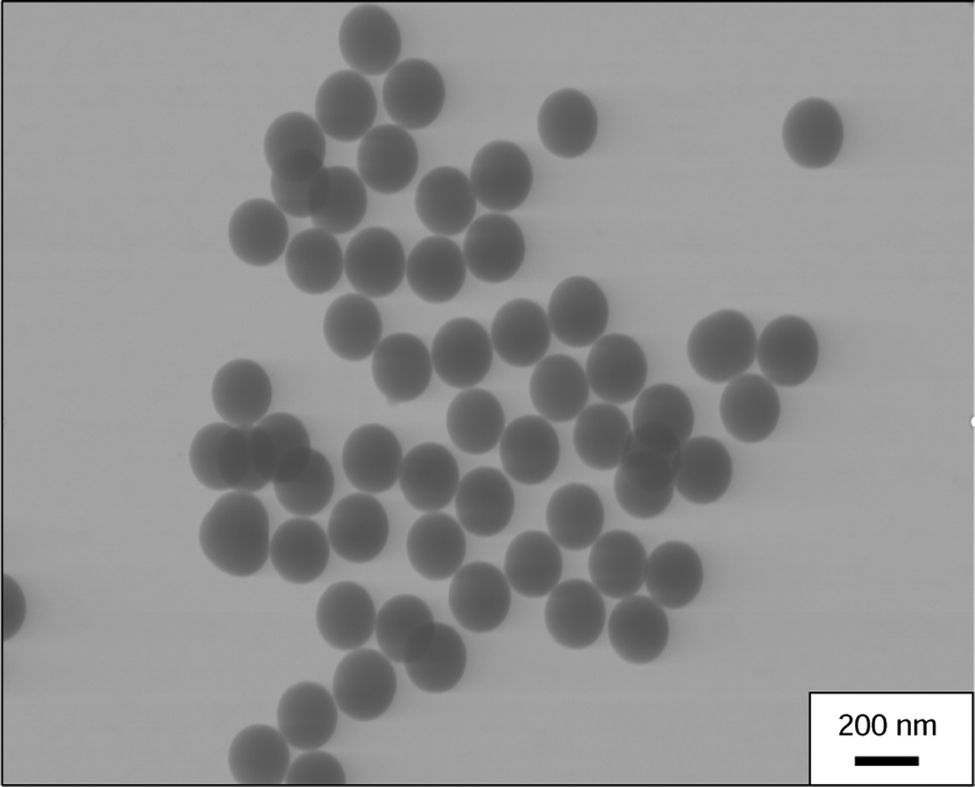 | ||
| Fig. 1 Typical electron micrograph of the sample SiO2 nanoparticles. The diameter is found to be 157 ± 6 nm with the uncertainty reflecting the standard deviation of the size distribution measured by STEM. | ||
The nanoparticle beam is crossed at right angle with the soft X-rays and the photoemission is recorded by a home-built magnetic-bottle time-of-flight electron spectrometer which is based on the design of Chesnovsky et al.37 This spectrometer has previously been described elsewhere.38,39
The Monte–Carlo simulations of electron transport in the nanoparticles were performed using the “Simulation of Electron Spectra for Surface Analysis” (SESSA) software.40 SESSA can be used to simulate photoelectron spectra with or without electron elastic scattering. For the simulations with elastic scattering turned “on”, the differential elastic scattering cross sections of Yates were used.41 The nanoparticles were modeled as spheres with a diameter of 150 nm. The reported density of 2.0 g cm−3 for SiO2 nanoparticles generated by the Stöber method is used for the simulations.42 For the simulations, the angular anisotropy parameter β is set to zero for all photon energies to account for the absence of angular information in the experiment due to the large collection angle of the magnetic bottle electron spectrometer. The validity of this simplifying assumption was checked by a comparison with simulations using the β reported by Yeh and Lindau,43 but using a simulated spectrometer opening angle of π, indicating that the results were indistinguishable from each other.
Results and discussion
Fig. 2 shows typical photoelectron spectra of isolated, single SiO2 nanoparticles prepared in a particle beam and subsequently ionized by soft X-rays above the Si 2p absorption edge for different photon energies. The photoelectron spectra are dominated by a smooth background due to secondary electrons, which result from inelastic scattering. In addition to the smooth signal due to secondary electrons, a distinct feature is found at a binding energy of 108 eV, which is assigned as emission of Si 2p electrons.38,44 No spin–orbit splitting is observed, which is in agreement with other studies on photoemission from both bulk amorphous SiO245 and SiO2 nanoparticles,13,38 where the lack of a doublet structure was attributed to the disorder of the material.45 To quantify the Si 2p photoemission as a function of photon energy, the spectra shown in Fig. 2 were normalized to the photon flux and the transmission of the magnetic-bottle electron spectrometer. The yield of Si 2p photoelectrons is taken as the area under the discrete feature in the photoelectron spectra. The Si 2p yield is shown in Fig. 3(a) as a function of photon energy (lower horizontal scale) and Si 2p kinetic energy (upper horizontal scale). | ||
| Fig. 2 Photoelectron spectra of SiO2 nanoparticles (d = 157 ± 6 nm) at several photon energies above the Si 2p absorption edge. The dashed blue curve is an extrapolation of the smooth background due to secondary electrons to highlight the sharp feature assigned to Si 2p emission. The spectra are normalized with respect to the photon flux and the decrease of the Si 2p yield is interpreted as being due to energy dependent modulations of the absorption cross section and the transport properties of photoelectrons in the nanoparticles. | ||
 | ||
| Fig. 3 (a) Yield of Si 2p photoelectrons from SiO2 nanoparticles as a function of the photoelectron kinetic energy normalized to the incident photon flux when tuning the photon energy in the range 118–248 eV, (b) Si 2p absorption cross section of SIO2 taken from the work of Filatova et al.,46 the Si 2p absorption threshold is marked by an arrow. | ||
The Si 2p signal shown in Fig. 3(a) displays a decrease with increasing photon energy, corresponding to increasing electron kinetic energy, which can be attributed to the variation of the photoabsorption cross section and the electron scattering properties in the nanoparticles prior to escape from the surface. In order to distinguish the effect of varying cross section and of attenuation from electron transport, we show in Fig. 3(b) the imaginary part of the complex refractive index of bulk SiO2 reported by Filtova et al.46 to explore whether the sharp decrease in Si 2p direct ionization intensity can be ascribed to a drop in Si 2p photoabsorption cross section. The broken line in Fig. 3(b) shows an extrapolation of the pre-edge contribution to account for valence shell absorption, which is non-negligible in the investigated photon energy range. A comparison of the photoelectron yield curve shown in Fig. 3(a) and the photoabsorption cross section depicted in Fig. 3(b) indicates that the drop in photoelectron yield cannot be explained solely by variations in Si 2p absorption cross section. This leads to the conclusion that the observed variations in yield are evidently influenced by electron transport properties of the nanoparticles (i.e., elastic and inelastic electron scattering). To quantify the influence of electron transport on the Si 2p yield, we normalize the curve shown in Fig. 3(a) to the Si 2p absorption cross section (cf.Fig. 3(b)). The results are shown as the red circles in Fig. 4(a). We interpret the variations in the photoelectron yield after accounting for the photoabsorption cross section to be due to electron kinetic energy dependent transport properties in the bulk of SiO2 nanoparticles. The result of this analysis qualitatively resembles the “universal curve”,18 displaying a minimum of the yield at 30–50 eV accompanied by a sharp increase towards lower kinetic energies of the emitted electrons and an increase of lower slope towards higher kinetic energies.
 | ||
| Fig. 4 (a) Si 2p yield from SiO2 nanoparticles in the electron kinetic energy range 10–140 eV. The data were normalized with respect to photon flux and absorption cross section σ. Red dots correspond to the experimental data. Full and broken curves are obtained from Monte–Carlo simulations, corresponding to simulated Si 2p yields from SiO2 nanoparticles with electron elastic scattering turned “off” and “on” during the simulations, respectively, (b) ratio of simulated Si 2p yield from SiO2 nanoparticles when elastic scattering is turned “on” and “off”, respectively. | ||
We conducted Monte–Carlo simulations on photoionization of SiO2 nanoparticles in order to explore the information contained in the experimental results regarding electron transport in SiO2 nanoparticles. This information can be retrieved from the cross section-normalized Si 2p yield. Here, we focus on the yield of unscattered Si 2p electrons while ignoring Si 2p electrons that have been scattered inelastically as well as any other electron emission channels. Fig. 4 shows the results from Monte–Carlo simulations for the Si 2p photoelectron. These apply to a particle diameter of d = 150 nm, where the absorption cross section in the simulations has been set to be identical for all electron kinetic energies and only the elastic and inelastic mean-free paths are varied. As a result, kinetic energy dependent modulations in the simulated yields are assigned to changes in electron transport properties, similar to the experimental results when normalizing the yield of emitted photoelectrons to the absorption cross section. Fig. 4(a) shows simulated yield curves with elastic scattering turned “on” (black full curve) and turned “off” (black broken curve) during the simulations to study the influence of elastic scattering. For these simulations, the recently published inelastic mean-free path of SiO2 reported by Astasauskas et al.47 was used, which made use of an algorithm developed by Penn.48 For the simulations with elastic scattering turned “on”, the elastic scattering cross sections of Yates41 were used. The experimentally obtained yield curve shown in Fig. 4(a) has been multiplied by an arbitrary factor to align it with the simulation results with the elastic scattering turned “on” (dashed curve in Fig. 4(a)) with the experimental results at 100 eV. This facilitates a comparison between the experimental and simulated results.
The data shown in Fig. 4 indicate that the simulated electron yield is lower when elastic scattering is turned “on” than when it is turned “off”. To quantify the influence of electron elastic scattering on the Si 2p yield, the ratios of simulated Si 2p yields when elastic scattering is turned “on” and “off” are shown in Fig. 4(b). A ratio of 1 would thus imply that elastic scattering does not influence the Si 2p yield. While the simulated photoelectron yield with elastic scattering “on” is lowered by a modest amount of 15% at Ekin = 100 eV, i.e., in a regime where elastic scattering is weak, the difference is more pronounced for low energy electrons, where elastic scattering is significantly stronger. This result indicates that considering electron elastic scattering is indispensable for a quantitative interpretation of photoemission of low energy electrons, since elastic scattering is stronger for slow electrons.
Having established that the transport properties of photoelectrons in nanoparticles influence the photoelectron yield, we study in greater detail what information can be extracted from the electron energy dependent Si 2p yield emitted from SiO2 nanoparticles. We first explore the interpretation of Kostko et al.,49 who argue that the photoelectron yield from nanoparticles is directly proportional to the electron inelastic mean-free path of the sample. In a similar experiment to the present one, these authors studied the C 1s photoemission from squalene nanoparticles and argue that if the photoabsorption cross section can be accounted for, the relative photoelectron yield is directly proportional to the inelastic mean-free path. In contrast to this, the present results from simulations indicate that when elastic scattering is included in the simulations, the yield is lowered compared to simulation results with the elastic scattering “off” (see Fig. 4(b)). Notably, the lowering of the simulated yield is not constant over the entire energy range studied, such that direct proportionality between the photoelectron yield and the inelastic mean-free path is not evident. Thus the conclusion can be drawn that the interpretation proposed by Kostko et al.49 is applicable only in the limit of negligible elastic scattering.
Another conclusion that can be drawn from the present results shown in Fig. 4 is that the simulated Si 2p yields using literature parameters fail to reproduce the experimental yield. Evidently, the simulations greatly overestimate the yield for low energy electrons when using the reported IMFP.47 In order to explain the experimental electron yields we then simulated the Si 2p yield for various settings of the inelastic mean-free path and for the electron kinetic energy range that was studied in the present experiments. Typical results of such simulations are shown in Fig. 5(a). Simulated Si 2p yields with elastic scattering turned “off” (green curve) and turned “on” are shown for electron kinetic energies 20 eV (black curve), 50 eV (blue curve), and 100 eV (red curve), respectively. The differential electron elastic cross sections used for the simulations for 20 eV, 50 eV, and 100 eV are shown in Fig. 5(b) and were computed by the method of Yates.41 The photoabsorption cross sections has been set to be identical for all cases so that differences in yield can be interpreted as being due to differences in electron transport properties.
 | ||
| Fig. 5 (a) Simulated Si 2p yield of SiO2 nanoparticles as function of the inelastic mean-free path. The photoabsorption cross section is kept constant for these simulations, so that variations in the yield are due to the changing electron transport properties, (b) The differential elastic scattering cross sections used for the simulations. | ||
It is evident from the simulation results shown in Fig. 5(a) that, for a given IMFP, the photoelectron yield increases as the electron kinetic energy increases. This can be explained by the greater influence of elastic scattering for slow electrons. Secondly, only in the case of simulations with the elastic scattering turned “off” there is a linear proportionality between the inelastic mean-free path and the Si 2p yield (see straight green line in Fig. 5(a)). However, if elastic scattering is included the slope of the Si 2p yield decreases as a function of the mean-free path. This result indicates that it is not possible to directly obtain the inelastic mean-free path of electrons from a photoelectron yield curve if elastic scattering has a non-negligible contribution. The reason for this behavior is evidently the increased influence of electron elastic scattering for lower kinetic energies of the emitted electrons.
Inelastic mean-free paths
Having shown that the simulated Si 2p yields presented in Fig. 4(a) fail to reproduce the experimental Si 2p yields, we determine in the next step which inelastic mean-free paths are able to explain the experimentally observed yields. Here, the Si 2p yield is simulated for the kinetic energy range studied in the experiments (10–140 eV). For each electron kinetic energy, the IMFP is varied in the simulations until agreement is found between the simulated and experimental Si 2p yields. The photoabsorption cross section in the simulations is set to be identical for all photon energies, which is similar to the experimental data which are normalized to the photoabsorption cross section. Since the yield scale of the simulations is arbitrary, one fixed point is needed to connect the experimental and simulated yields. We used for this procedure parameters, which provides agreement with the modeled curves at 100 eV kinetic energy, i.e., an inelastic mean-free path value of 7.8 Å at Ekin = 100 eV. This value was obtained from the TPP-2M formula of Tanuma, Powell, and Penn26 using a band gap of 9 eV and a density of 2 g cm−3.42 The inelastic mean-free paths obtained from this procedure are presented in Fig. 6 (red dots). | ||
| Fig. 6 Electron inelastic mean-free paths (IMFP) in SiO2. The red symbols correspond to IMFP derived from the Si 2p yield of SiO2 nanoparticles (see Fig. 4). Various inelastic mean-free paths based on theory taken from the literature are shown for a comparison, as taken from: Astasauskas et al. (grey and magenta curves),47 Ashley and Anderson (green curve),51 Tanuma et al. (red curve),52 and the NIST database (blue line).26 The grey data points are experimental values taken from Seiffert et al.50 The modeled curves are in agreement with the experimental data for Eking > 100 eV, but there is a large spread in the results for low energy electrons and deviations from the experimental data (see text for further details). | ||
Results from several theoretical studies of the inelastic mean-free paths of electrons in SiO2 are shown in Fig. 6 in comparison with results derived from the experimental data (red dots). The theoretical values show a large disagreement to the experimental results for low electron kinetic energies, where the relative differences can reach several hundred percent. In addition, there are also significant differences between the results derived from theoretical studies. These discrepancies underscore the need for reliable experimental data on low energy photoelectron transport in nanoparticles. It is also of interest to compare the present results to earlier experimental data of Seiffert et al.50 who determined the inelastic mean-free paths of 20–30 eV photoelectrons in SiO2 nanoparticles after valence shell ionization. This previous study covered a narrower energy range and was performed using a different experimental approach, namely attosecond chronoscopy.50 At 20 eV, there is fair agreement between the presently derived inelastic mean-free paths and those obtained by Seiffert et al.50 The results of Seiffert et al., however, indicate an almost constant inelastic mean-free path in the electron kinetic energy range of 20–30 eV. Contrary to this, the present results indicate that a drop in inelastic mean-free paths over this electric kinetic energy range, which is qualitatively similar in slope to what is shown in the theory curves and what the “universal curve” predicts, which means that there is a drop in inelastic mean-free path from 20 eV to 30 eV.
Photoemission depth distribution and mean escape depth
The high surface sensitivity of photoelectron spectroscopy is useful for materials characterization, using, e.g., depth profiling. For quantitative interpretation of nanoparticle photoelectron spectroscopy, it is imperative to be able to quantify the depth distribution of photoemission, i.e., the depth of the thin surface region that contributes to the photoemission signal. For macroscopic samples with planar surface in the absence of elastic scattering, the electron attenuation is often modeled by an exponential function,19 with the probability of photoelectrons reaching the surface diminishing if they are generated deep in the bulk. If elastic scattering is non negligible and/or the surface of macroscopic samples is not planar, this model may not be applicable. In the present case of SiO2 nanoparticles, the geometry of the samples and elastic electron scattering may modulate the photoemission depth profile and thus influence the interpretation of results. We investigate in the following what the present energy dependent Si 2p yields coupled with Monte–Carlo simulations of electron transport can reveal about the surface sensitivity of the experimental results. This requires to simulating the depth distribution of photoemission. For these simulations, the Si 2p emission from a 0.1 Å layer in d = 150 nm SiO2 nanoparticles is monitored. These simulations were repeated while moving this layer deeper inwards towards the center of the spherical nanoparticles. The emission of electrons which does not originate from this specific thin layer is disregarded in this simplified analysis. Note that this approach is inspired by previous work on simulating photoelectron depth distributions.40,53 For the simulations of the photoemission depth distribution, the inelastic mean-free paths shown in Fig. 6 and the elastic mean-free path of Yates were used.41 The obtained depth distribution functions (DDF) are shown in Fig. 7. The magnitude of the DDF indicates the probability of emitted electrons originating from this depth layer and the integral over the entire curve corresponds to the photoelectron yield. Shown are typical depth distribution functions for the electron kinetic energies 20 eV and 100 eV, respectively. These energies are of interest to a comparison with the experimental data, since the Si 2p yield is similar to within 3% for these two energies (see Fig. 4(a)) whereas the effect of elastic scattering is expected to be enhanced at 20 eV compared to 100 eV (see Fig. 5(b)). | ||
| Fig. 7 (a) Simulated depth distribution functions of Si 2p electrons from d = 150 nm SiO2 spherical nanoparticles. Only electrons that escape without undergoing inelastic scattering are considered. The signal amplitude from deeper surfaces is lowered due to attenuation of electron emission. Although the yield for the two considered energies (20 eV and 100 eV) is identical to within 3% (see Fig. 4), the depth distribution of the signal is significantly different. The arrows mark the electron mean escape depth, (b) Same as (a), but plotted on a logarithmic vertical axis, (c) Same as (a) but with the elastic scattering turned “on” for the simulations, (d) Same as (c) but with a logarithmic vertical axis. | ||
Fig. 7(a) and (b) shows on a linear and logarithmic scale, respectively, the simulated depth distribution functions of Si 2p photoemission from SiO2 nanoparticles when elastic scattering is turned “off” during the simulations. The depth distribution functions shown in Fig. 7(a) and (b) indicate that, in contrast to the expectation for emission from planar samples using a negligible acceptance angle, that the depth distribution function is non-exponential even in the absence of elastic scattering, i.e., the slopes of the curves plotted on a logarithmic scale in Fig. 7(b) are not constant. This can be understood as a result of the spherical shape of the nanoparticle samples on photoemission. For a macroscopic sample with a planar surface using a negligible acceptance angle when elastic scattering is also negligible, the depth distribution function (DDF) can be considered to be DDF ∝ exp(−z/λ![[thin space (1/6-em)]](https://www.rsc.org/images/entities/char_2009.gif) cosα), where λ is the inelastic mean-free path, α is the emission angle with respect to the surface normal, and z is the depth.54 Due to the curvature of the surface of spherical nanoparticles investigated in the present experiments, the emission angle α varies across the surface, from α = 0 at the pole of the spheres facing the spectrometer to α = π/2 at the equator of the spheres. Effects of the polarization of the soft X-rays are not expected to be of importance due to the large collection angle of the used magnetic-bottle-type electron spectrometer. The recorded photoemission thus stems from locations with different emission angles with respect to the surface normal. This leads to a depth distribution function of the recorded signal, which is a sum of exponential functions covering different values of cosα, which cannot be described by a single exponential function. Effective attenuation lengths, which are often used to characterize surface sensitivity of photoemission experiments,55 can be used if the depth distribution is exponential, which is evidently not the case for nanoparticles. Since the effective attenuation length (EAL) is not a suitable way to quantify the surface sensitivity for the present samples, we quantify the mean escape depth (MED) of photoemission instead. The red (20 eV) and black (100 eV) arrows in Fig. 7 mark the mean escape depths of photoelectrons, which are defined by the expectation value of the depth from which the detected photoelectrons originate, given by
cosα), where λ is the inelastic mean-free path, α is the emission angle with respect to the surface normal, and z is the depth.54 Due to the curvature of the surface of spherical nanoparticles investigated in the present experiments, the emission angle α varies across the surface, from α = 0 at the pole of the spheres facing the spectrometer to α = π/2 at the equator of the spheres. Effects of the polarization of the soft X-rays are not expected to be of importance due to the large collection angle of the used magnetic-bottle-type electron spectrometer. The recorded photoemission thus stems from locations with different emission angles with respect to the surface normal. This leads to a depth distribution function of the recorded signal, which is a sum of exponential functions covering different values of cosα, which cannot be described by a single exponential function. Effective attenuation lengths, which are often used to characterize surface sensitivity of photoemission experiments,55 can be used if the depth distribution is exponential, which is evidently not the case for nanoparticles. Since the effective attenuation length (EAL) is not a suitable way to quantify the surface sensitivity for the present samples, we quantify the mean escape depth (MED) of photoemission instead. The red (20 eV) and black (100 eV) arrows in Fig. 7 mark the mean escape depths of photoelectrons, which are defined by the expectation value of the depth from which the detected photoelectrons originate, given by  , where α is the emission angle and z is the depth.56 The MED, in contrast to the EAL, is thus also well-defined for non-exponential depth distributions. For the two photon energies considered in Fig. 7 with inelastic mean-free paths of 9.1 Å (20 eV) and 7.8 Å (100 eV), respectively, the MEDs are found to be lowered compared to the IMFP, even in the absence of elastic scattering (see arrows in Fig. 7(a)). This shortening of the MED compared to the IMFP in the absence of elastic scattering is caused by the spherical nanoparticle geometry. Thus, the spherical shape of the nanoparticles causes a lower mean escape depth. Shard et al. proposed that the mean escape depth is shorter in spheres compared to planar bulk solids by a factor of 0.67, and was termed as “topofactor” in ref. 10,27. This estimate seems reasonable, as the MED/IMFP is found here to be 0.69 for Ekin = 20 eV and 0.60 for Ekin = 100 eV.
We next discuss the influence of electron elastic scattering on the photoemission depth distribution function. Fig. 7(c) and (d) show simulated depth distribution functions, when the elastic scattering is included in the simulations (turned “on”) on a linear and logarithmic scale, respectively. It is evident from the depth distribution functions in Fig. 7(c) and (d) that the emission originating from atoms closest to the surface, i.e., at small depths, is enhanced relative to the simulations when elastic scattering is “off”. In addition, the probability of escape for electrons created at shallow depths is enhanced for 20 eV compared to 100 eV, whereas the signal from surface emission shows no kinetic energy dependence when elastic scattering is neglected during the simulations (see Fig. 7(a) and (b)).
The effect of the elastic electron scattering on the photoemission depth distribution function can be understood by considering two separate effects by which the elastic scattering influences the depth distribution. These are: (i) elastic backscattering, which increases the signal from small depths since photoelectrons that otherwise would be emitted away from the surface and not get detected are backscattered towards the surface and may escape the nanoparticles, and (ii) the longer the pathlength traveled by photoelectrons caused by elastic scattering, the higher is the reduction in signal since the probability of inelastic scattering is increased. For shallow depths, effect (i) evidently dominates, while for deeper depths effect (ii) dominates.57 This result is qualitatively similar to previously reported observations for bulk samples, if elastic scattering is strong.24 The mean escape depths for 20 eV and 100 eV are indicated by arrows in Fig. 7(c) and (d). Even though the photoelectron yield is similar for both energies, the MED is shorter for 20 eV electrons due to elastic backscattering of electrons. This demonstrates that the relationship between yield, IMFP, and MED becomes complex when elastic scattering is strong, as is the case for slow electrons. Ottosson et al.58 and Suzuki et al.59 reported energy dependent O 1s photoelectron yields from water in a liquid microjet. They argue that the photoelectron yield is directly proportional to the effective attenuation length (EAL) of the photoelectrons, which is the case if the depth distribution function can be described by an exponential function of the form exp(−EAL/d) where d is the depth below the surface of the sample and EAL is energy dependent. This assumption is only valid if the depth distribution function is sufficiently close to an exponential, i.e., if elastic scattering is weak. The data shown in Fig. 7(c) and (d) indicate that this assumption may not hold if elastic scattering is non-negligible, since strong elastic scattering causes the MED to be different although the photoelectron yield is identical.
Fig. 8 shows the mean escape depths of Si 2p photoelectrons from SiO2 nanoparticles for the electron kinetic energy range 10–140 eV extracted from DDF curves similar to those shown in Fig. 7(c) and (d). For a comparison, Fig. 8 also includes mean escape depths computed using the NIST EAL database25 for a macroscopic planar sample and normal emission covering the kinetic energy range above 50 eV (dark green curve). To account for the surface curvature effect occurring in spherical nanoparticles, the MED results from the NIST database have been multiplied by a “topofactor” of 0.67 as suggested by Shard et al.10,27 For the energy range where the NIST database is applicable (Ekin > 50 eV), there is agreement between the present results and the data from the NIST database if the “topofactor” is taken into account. For kinetic energies below 50 eV, a direct comparison with the data from the NIST database is thus not possible. The observed increase in the MED towards low kinetic energies indicates that the surface sensitivity of the experiment is decreased for lower electron kinetic energies. In order to assess if the increase in escape depth towards lower energies is directly proportional to the Si 2p yield, as was hypothesized for photoemission from water in a liquid microjet,58,59 it is necessary to display the escape depth and the Si 2p yield in a single Figure for a comparison, which is done below.
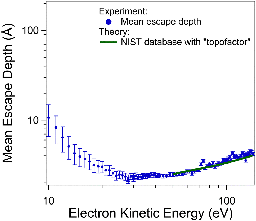 | ||
| Fig. 8 Mean escape depth of Si 2p photoelectrons from spherical SiO2 nanoparticles (d = 157 ± 6 nm). The mean escape depths are obtained from depth distribution functions similar to the ones shown in Fig. 7. For a comparison, the mean escape depth obtained from the NIST EAL database is shown in the energy range >50 eV, which is the lowest energy covered by this database.25 | ||
Fig. 9 shows a comparison of the relative values for the Si 2p photoelectron yield, the inelastic mean-free path, and the mean escape depth for SiO2 nanoparticles obtained from the present work. The data shown in previous Figures have been normalized to take the value of unity for Ekin = 100 eV. This normalization facilitates the comparison of the relative changes and allows for testing the assumptions proposed by other authors that IMFP or MED are directly proportional to the photoelectron yield.49,58,59 It is evident from the data presented in Fig. 9 that an assumption of direct proportionality between the photoelectron yield and the inelastic mean-free path or the photoelectron escape depth is reasonable above ca. 50 eV. For lower energies, however, such assumption leads to increased errors. The lack of direct proportionality is attributed mainly to the effect of elastic electron scattering, as discussed in detail above. Thus, for photoelectron spectroscopy using photoelectrons below 50 eV, a more thorough analysis of photoelectron spectra is needed if quantitative information about, e.g., sample elemental composition is to be obtained. We have demonstrated that Monte–Carlo simulations of electron transport can be utilized to extract IMFP and MED from experimentally obtained photoelectron yields taken at different photon energies. In the context of the previously proposed direct proportionality between IMFP and electron yields in nanoparticles49 or the direct proportionality between photoelectron yield and EAL in water,58 we can conclude that neither assumption is correct for SiO2 nanoparticles for electron energies below 50 eV because of the strong and energy dependent influence of elastic scattering.
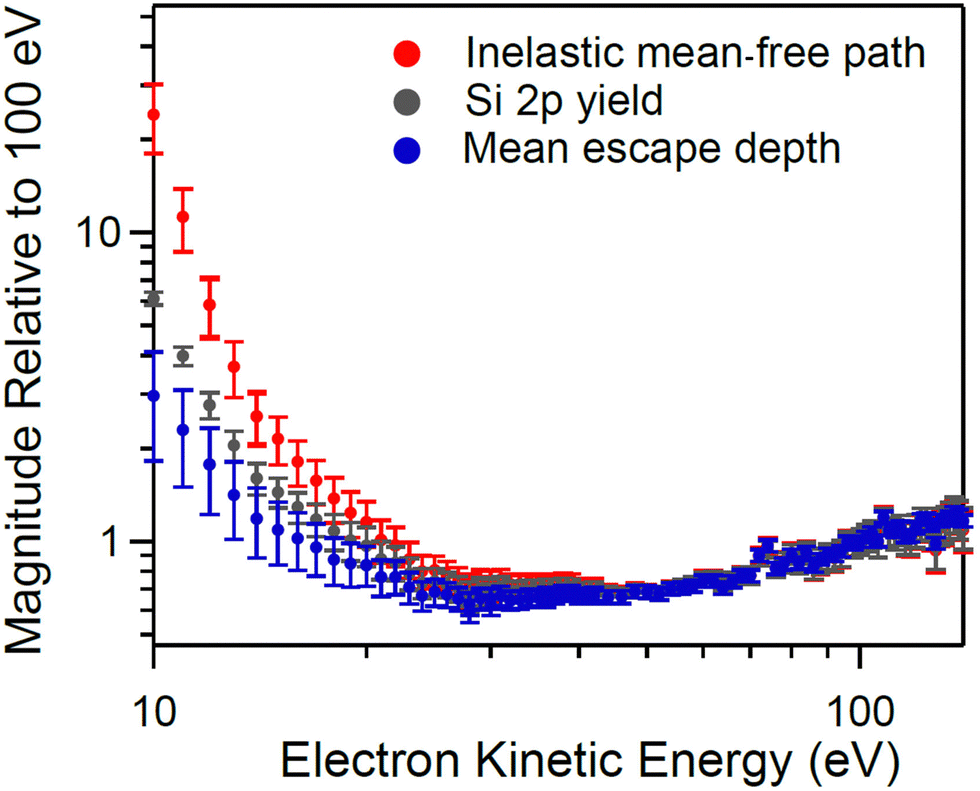 | ||
| Fig. 9 A comparison of relative IMFP, MED, and Si 2p photoelectron yield over the studied kinetic energy range. The quantities have been multiplied by an arbitrary factor to align them to unity at Ekin = 100 eV. For Ekin < 50 eV, the curves increasingly diverge, indicating that using photoelectron yields to directly infer IMFP or MED can lead to large errors for low kinetic energies, where elastic scattering is strong. | ||
Conclusions
In conclusion, we have presented Si 2p photoelectron yields from SiO2 nanoparticles in the kinetic energy range 10–140 eV generated by photoionization by 118–248 eV soft X-rays. The Si 2p photoelectron yields display a pronounced dependence on the electron kinetic energy, which are attributed to the energy dependence of the absorption cross section and the photoelectron transport properties (i.e., elastic and inelastic electron scattering). By normalizing the results to the photon flux and the absorption cross section, the effect of the electron transport is quantified.By a comparison with Monte–Carlo simulations of the electron transport in the nanoparticles we obtain the inelastic mean-free paths of 10–140 eV photoelectrons in the nanoparticle sample, in an energy region where experimental IMFPs are notoriously scarce. The comparison with published IMFPs from theoretical predictions indicates that the published studies overestimate the IMFP for low energy photoelectrons. Furthermore, fair agreement is found with the experimental estimate published by Seiffert et al.50 who studied a narrower electron kinetic energy range.
Simulations of the depth distribution of the photoemission showed that the photoelectron yield is directly proportional neither to the inelastic mean-free path nor to the escape depth of the photoelectrons, which is contrary to previously published interpretations of energy dependent photoelectron yields of condensed phase samples. The reason for this lack of proportionality is the strong effect of electron elastic scattering for low energy electrons. Simulations of the photoelectron transport in the nanoparticles reveal that the depth distribution function of the photoemission is non-exponential, which renders the use of an effective attenuation length ambiguous. Instead, we characterize the surface sensitivity of the photoemission by the mean escape depth. The mean escape depth is found to be shortened due to electron elastic scattering and to be markedly lower than what would be expected for bulk samples due to the non-planar surface geometry of the spherical nanoparticles under investigation. We highlight that care needs to be taken if the methodology for interpreting photoemission results used for planar surfaces of macroscopic solids is to be used to interpret results on curved surfaces of nanoparticles.
Conflicts of interest
There are no conflicts to declare.Acknowledgements
Financial support by BMBF (grant numbers: 05K13KE2, 05K16KEA, and 05K16VHB) is gratefully acknowledged. We thank the Helmholtz Zentrum Berlin for the allocation of synchrotron radiation beamtime and J. Viefhaus for technical assistance during the experiments.References
- H. Zhang and G. Zhu, Appl. Surf. Sci., 2012, 258, 4952–4959 CrossRef CAS
.
- A. Milosavljevic, D. K. Bozanic, S. Sadhu, N. Vukmirovic, E. Dojcilovic, P. Sapkota, W. Huang, J. D. Bozek, C. Nicolas, L. Nahon and S. Ptasinska, J. Phys. Chem. Lett., 2018, 9, 3604–3611 CrossRef CAS PubMed
- E. Antonsson, M. Patanen, C. Nicolas, J. J. Neville, S. Benkoula, A. Goel and C. Miron, Phys. Rev. X, 2015, 5, 011025 Search PubMed
- F.-X. Ouf, P. Parent, C. Laffon, I. Marhaba, D. Ferry, B. Marcillaud, E. Antonsson, S. Benkoula, X.-J. Liu, C. Nicolas, E. Robert, M. Patanen, F.-A. Barreda, O. Sublemontier, A. Coppalle, J. Yon, F. Miserque, T. Mostefaoui, T. Z. Regier, J. B. A. Mitchell and C. Miron, Sci. Rep., 2016, 6, 36495 CrossRef CAS PubMed
- A. R. Abid, M. Reinhardt, N. Boudjemia, E. Pelimanni, A. Milosavljevic, C. M. Saak, M. Huttula, O. Björneholm and M. Patanen, RSC Adv., 2021, 11, 2103–2111 RSC
- A. Levy, M. De Anda Villa, G. Laurens, V. Blanchet, J. D. Bozek, J. Gaudin, E. Lamour, S. Mace, P. Mignon, A. Milosavljevic, C. Nicolas, M. Patanen, C. Prigent, E. Robert, S. Steydli, M. Tassinelli, D. Vernhet, O. Veteläinen and D. Amans, Langmuir, 2021, 37, 5783–5794 CrossRef CAS PubMed
- K. Qadir, S. H. Joo, B. S. Mun, D. R. Butcher, J. R. Renzas, F. Aksoy, Z. Liu, G. A. Somorjai and J. Y. Park, Nano Lett., 2012, 12, 5761–5768 CrossRef CAS PubMed
- C. Evangelista, N. Panziera, P. Pertici, G. Vitulli, P. Salvadori, C. Battoccio and G. Polzonetti, J. Catal., 2009, 262, 287–293 CrossRef
- M. Chadzicki, W. S. M. Werner, A. G. Shard, Y.-C. Wang, D. G. Castner and C. J. Powell, J. Phys. Chem. C, 2015, 119, 17687–17696 CrossRef PubMed
- A. G. Shard, J. Phys. Chem. C, 2012, 116, 16806–16813 CrossRef CAS
- I. Tunc, S. Suzer, M. A. Correa-Duarte and L. M. Liz-Marzán, J. Phys. Chem. B, 2005, 109, 7597–7600 CrossRef CAS PubMed
- W. S. Werner, M. Chudzicki, W. Smekal and C. J. Powell, Appl. Phys. Lett., 2014, 104, 243106 CrossRef
- E. Antonsson, B. Langer, I. Halfpap, J. Gottwald and E. Rühl, J. Chem. Phys., 2017, 146, 244301 CrossRef CAS PubMed
- A. Müller, K. Sparnacci, W. E. S. Unger and S. Tougaard, Surf. Interface Anal., 2020, 52, 770–777 CrossRef
- K. R. Wilson, S. L. Zou, J. N. Shu, E. Rühl, S. R. Leone, G. C. Schatz and M. Ahmed, Nano Lett., 2007, 7, 2014–2019 CrossRef CAS
- D. K. Bozanic, G. A. Garcia, O. Sublemontier, J. Pajovic, V. Djokovic and L. Nahon, J. Phys. Chem. C, 2020, 124, 24500–24512 CrossRef CAS
- C. J. Powell and A. Jablonski, J. Phys. Chem. Ref. Data, 1999, 28, 19–62 CrossRef CAS
- M. P. Seah and W. A. Dench, Surf. Interface Anal., 1979, 1, 2–11 CrossRef CAS
- A. Jablonski and C. J. Powell, J. Electron Spectrosc. Relat. Phenom., 1999, 100, 137–160 CrossRef CAS
- C. J. Powell and A. Jablonski, Nucl. Instrum. Methods Phys. Res., Sect. A, 2009, 601, 54–65 CrossRef CAS
- C. J. Powell, W. S. M. Werner, A. G. Shard and D. G. Castner, J. Phys. Chem. C, 2016, 120, 22730–22738 CrossRef CAS PubMed
- H. Shimada, N. Matsubayashi, M. Imamura, M. Suzuki, Y. Higashi, H. Ando, H. Takenaka, S. Kurosawa, S. Tanuma and C. J. Powell, Surf. Interface Anal., 2000, 29, 336–340 CrossRef CAS
- C. J. Powell and A. Jablonski, Surf. Sci., 2001, 488, L547–L552 CrossRef CAS
- W. H. Gries and W. Werner, Surf. Interface Anal., 1990, 16, 149–153 CrossRef CAS
-
C. J. Powell and A. Jablonski, NIST Electron Effective-Attenuation-Length Database, Version 1.3 SRD 82, National Institue of Standards and Technology, Gaithersburg, MD, 2011 Search PubMed
-
C. J. Powell and A. Jablonski, NIST Electron Inelastic-Mean-Free-Path Database – Version 1.2, National Institute of Standards and Technology, Gaithersburg, 2010 Search PubMed
- A. G. Shard, J. Wang and S. J. Spencer, Surf. Interface Anal., 2009, 41, 541–548 CrossRef CAS
- W. Stöber, A. Fink and E. Bohn, J. Colloid Interface Sci., 1968, 26, 62 CrossRef
- A. P. Philipse, Colloid Polym. Sci., 1988, 266, 1174–1180 CrossRef CAS
- E. Antonsson, H. Bresch, R. Lewinski, B. Wassermann, T. Leisner, C. Graf, B. Langer and E. Rühl, Chem. Phys. Lett., 2013, 559, 1–11 CrossRef CAS
- P. Liu, P. J. Ziemann, D. B. Kittelson and P. H. McMurry, Aerosol Sci. Technol., 1995, 22, 293–313 CrossRef CAS
- B. Langer, C. Raschpichler, M. Gruner, E. Antonsson, C. Goroncy, C. Graf and E. Rühl, Z. Phys. Chem., 2016, 230, 1249–1267 CrossRef CAS
- C. Raschpichler, C. Goroncy, B. Langer, E. Antonsson, B. Wassermann, C. Graf, P. Klack, T. Lischke and E. Rühl, J. Phys. Chem. C, 2020, 124, 16663–16674 CrossRef CAS
- H. Bresch, B. Wassermann, B. Langer, C. Graf, R. Flesch, U. Becker, B. Österreicher, T. Leisner and E. Rühl, Faraday Discuss., 2008, 137, 389–402 RSC
-
E. Antonsson, Doctoral Thesis, Freie Universität, Berlin, 2011
- B. L. Henke, E. M. Gullikson and J. C. Davis, At. Data Nucl. Data Tables, 1993, 54, 181–342 CrossRef CAS
- O. Chesnovsky, S. H. Yang, C. L. Pettiette, M. J. Craycraft and R. E. Smalley, Rev. Sci. Instrum., 1987, 58, 2131–2137 CrossRef
- J. Meinen, S. Khasminskaya, M. Eritt, T. Leisner, E. Antonsson, B. Langer and E. Rühl, Rev. Sci. Instrum., 2010, 81, 085107 CrossRef PubMed
- E. Antonsson, C. Raschpichler, B. Langer, D. Marchenko and E. Rühl, J. Phys. Chem. A, 2018, 122, 2695–2702 CrossRef CAS PubMed
-
W. S. M. Werner, W. Smekal and C. J. Powell, NIST Database for the Simulation of Electron Spectra for Surface Analysis, Version 2.1, National Institute of Standards and Technology, Gaithersburg, Maryland, 2016 Search PubMed
- A. C. Yates, Comput. Phys. Commun., 1971, 2, 175 CrossRef CAS
- A. v Blaaderen and A. P. M. Kentgens, J. Non-Cryst. Solids, 1992, 149, 162 Search PubMed
- J. J. Yeh and I. Lindau, At. Data Nucl. Data Tables, 1985, 32, 1–155 CrossRef CAS
- A. Bianconi, Surf. Sci., 1979, 89, 41 CrossRef CAS
- Z. H. Lu, P. McCaffrey, B. Brar, G. D. Wilk, R. M. Wallace, L. C. Feldman and S. P. Tay, Appl. Phys. Lett., 1997, 71, 2764–2766 CrossRef CAS
- E. Filatova, V. Lukyanov, R. Barschewitz, J. M. Andre, M. Idir and P. Stemmler, J. Phys.: Condens. Matter, 1999, 11, 3355 CrossRef CAS
- V. Astasauskas, A. Bellissimo, P. Kuksa, C. Tomastik, H. Kalbe and W. S. M. Werner, J. Electron Spectrosc. Relat. Phenom., 2020, 241, 146829 CrossRef CAS
- D. R. Penn, Phys. Rev. B: Condens. Matter Mater. Phys., 1987, 35, 482–486 CrossRef CAS PubMed
- O. Kostko, M. I. Jacobs, B. Xu, K. R. Wilson and M. Ahmed, J. Chem. Phys., 2019, 151, 184702 CrossRef CAS PubMed
- L. Seiffert, Q. Liu, S. Zherebtsov, A. Trabattoni, P. Rupp, M. C. Castrovilli, M. Galli, F. Sussmann, K. Wintersperger, J. Stierle, G. Sansone, L. Poletto, F. Frassetto, I. Halfpap, V. Mondes, C. Graf, E. Rühl, F. Krausz, M. Nisoli, T. Fennel, F. Calegari and M. F. Kling, Nat. Phys., 2017, 13, 766–770 Search PubMed
- J. C. Ashley and V. E. Anderson, J. Electron Spectrosc. Relat. Phenom., 1981, 24, 127–148 CrossRef CAS
- S. Tanuma, C. J. Powell and D. R. Penn, Surf. Interface Anal., 1991, 17, 927 CrossRef CAS
- J. Zemek, P. Jiricek, S. Hucek, A. Jablonski and B. Lesiak, Surf. Sci., 2001, 473, 8–16 CrossRef CAS
- A. Jablonski and C. J. Powell, Surf. Sci. Rep., 2002, 47, 33–91 CrossRef CAS
- A. Jablonski and C. J. Powell, J. Electron Spectrosc. Relat. Phenom., 2017, 218, 1–12 CrossRef CAS PubMed
- C. J. Powell and A. Jablonski, J. Electron Spectrosc. Relat. Phenom., 2010, 178–179, 331–346 CrossRef CAS
- A. Jablonski and S. Tougaard, Surf. Interface Anal., 1998, 26, 17–29 CrossRef
- N. Ottosson, M. Faubel, S. E. Bradforth, P. Jungwirth and B. Winter, J. Electron Spectrosc. Relat. Phenom., 2010, 177, 60–70 CrossRef CAS
- Y.-I. Suzuki, K. Nishizawa, N. Kurahashi and T. Suzuki, Phys. Rev. E: Stat., Nonlinear, Soft Matter Phys., 2014, 90, 010302(R) CrossRef PubMed
| This journal is © the Owner Societies 2023 |