
 Open Access Article
 This Open Access Article is licensed under a Creative Commons Attribution-Non Commercial 3.0 Unported Licence
ZnSe and ZnTe as tunnel barriers for Fe-based spin valves
Gokaran
Shukla
a,
Hasan M.
Abdullah
a,
Avijeet
Ray
a,
Shubham
Tyagi
a,
Aurélien
Manchon
 b,
Stefano
Sanvito
c and
Udo
Schwingenschlögl
*a
b,
Stefano
Sanvito
c and
Udo
Schwingenschlögl
*a
aKing Abdullah University of Science and Technology (KAUST), Physical Science and Engineering Division (PSE), Thuwal 23955-6900, Saudi Arabia. E-mail: gokaran.shukla@kaust.edu.sa; udo.schwingenschlogl@kaust.edu.sa
bAix-Marseille Université, CNRS, CINaM, Marseille, France
cSchool of Physics, AMBER and CRANN Institute, Trinity College, Dublin 2, Ireland. E-mail: sanvitos@tcd.ie
First published on 3rd May 2023
Abstract
Owing to their use in the optoelectronic industry, we investigate whether ZnSe and ZnTe can be utilised as tunnel barrier materials in magnetic spin valves. We perform ab initio electronic structure and linear response transport calculations based on self-interaction-corrected density functional theory for both Fe/ZnSe/Fe and Fe/ZnTe/Fe junctions. In the Fe/ZnSe/Fe junction the transport is tunneling-like and a symmetry-filtering mechanism is at play, implying that only the majority spin electrons with Δ1 symmetry are transmitted with large probability, resulting in a potentially large tunneling magnetoresistance (TMR) ratio. As such, the transport characteristics are similar to those of the Fe/MgO/Fe junction, although the TMR ratio is lower for tunnel barriers of similar thickness due to the smaller bandgap of ZnSe as compared to that of MgO. In the Fe/ZnTe/Fe junction the Fermi level is pinned at the bottom of the conduction band of ZnTe and only a giant magnetoresistance effect is found. Our results provide evidence that chalcogenide-based tunnel barriers can be utilised in spintronics devices.
I. Introduction
ZnSe and ZnTe are extensively used semiconductors in thin-film solar cells and optoelectronics devices operating in the blue and green regions of the visible spectrum.1–3 Both compounds exhibit high electron mobility (ZnSe, 200–280 cm2 V−1 s−1; ZnTe, 340 cm2 V−1 s−1) and low reflectance4 for large photo-generated currents for both p and n-type dopants.5–10 In addition, these semiconductors possess a small carrier effective mass at the Γ-point, a property used for the enhancement of infrared-laser optical gains by Cr doping11,12 and high energy X-ray and gamma-ray detectors.1,10,13,14 Here we explore the possibility to integrate the materials into spintronics devices.In spintronics one controls the device operation and performance using both the electron charge and spin.15,16 The most common device is perhaps the magnetic tunnel junction (MTJ), which consists of two ferromagnetic leads separated by a thin tunnel barrier. An MTJ exhibits low (high) resistance when the magnetic vectors of the two leads are oriented parallel (anti-parallel). There is the possibility to swap the sign of the signal by appropriate choice of the leads and tunnel barrier.17 In binary terms, a low (high) resistance maps to a 0 (1). The magnetoresistance effect in MTJs is the backbone of current spintronics devices, such as magnetic random access memories (MRAMs),18 microwave generators,19 stochastic oscillators,20 neuromorphic computers,21–24 MRAM-based ultrafast embedded memories,25 spin-based NANDs,26 non-volatile flip-flops,27–29 non-volatile full adders,30 non-uniform clock generators,31 radio frequency spectrum optimizers,32 spin transfer torque devices,33,34 magnetic sensors,35 comparators,36 thermal sensors,37 and analog-to-digital converters.38–40 Non-volatility,18 low power consumption,41 large area scalability,41 and practically infinite endurance42 make MTJs promising candidates for memory elements in nano-electronics.
The main quality factor of a MTJ is the tunneling magneto resistance ratio,  , where GP (GAP) is the total conductance in the parallel (P) (anti-parallel; AP) configuration. The total conductance can be written as sum of the spin-majority and spin-minority contributions, following a two-spin-fluid approximation that neglects spin-flip scattering, GP(AP) = GP(AP)↑ + GP(AP)↓, with GP(AP)σ being the conductance for spin σ. In the nineties, MTJs were mostly based on amorphous Al2O3 tunnel barriers.43,44 The TMR ratio in these devices is
  in Julliere's model, which is valid for thick and high enough tunnel barriers. P1 and P2 denote the spin-polarized densities of states in the two magnetic leads at the Fermi level, EF.45 In general,
  , where nσ is the density of states at EF for spin σ.46 Since P in most transition-metal ferromagnets hardly exceeds 50%, the TMR ratio of an amorphous tunnel barrier is limited to ∼70%. This, however, does not apply to crystalline tunnel barriers in which the TMR ratio is determined by the symmetry-filtering mechanism.47,48
In a crystalline tunnel barrier the transverse wave vector, k‖, remains a good quantum number. This means that only the longitudinal kz component of the wave vector (which is complex in an insulator) changes across the barrier, while the transverse component is conserved. Symmetry-filtering then allows Bloch states with a certain angular momentum to tunnel with higher probability than others.47,49,50 The angular-momentum-dependent tunneling probability is mainly governed by the overlap integral between the wavefunction of the incident electron and the wavefunctions at the valence band maximum and conduction band minimum of the tunneling barrier.49 In the case of exact symmetry matching the overlap integral is maximal, resulting in high tunneling probability.49 Notably, the current commercial MTJs are mostly based on the Fe/MgO/Fe junction,51,52 in which the exact symmetry matching condition is fulfilled. In this case the Δ1↑ states tunnel with higher probability than the Δ5↑ and Δ2↓ states, while the Δ1↓ states are not available in Fe at EF.47 This means that the tunnel current is completely spin-polarized for a thick enough MgO tunnel barrier.
In addition to the Fe/MgO/Fe junction, the symmetry-filtering argument has been tested in various wide bandgap oxide and multiferroic MTJs.53–62 There are many reasons behind the success of the Fe/MgO/Fe junction in spintronics, particularly the ease of lattice-matched crystalline growth, the large in-plane/perpendicular magneto-crystalline anisotropy, the wide bandgap of MgO, and the availability of a controlled lithographic process for large area. However, the Fe/MgO/Fe junction also encounters limitations at the fabrication level. In particular, growing a compound with four-fold rotation symmetry (C4) on a compound with six-fold rotation symmetry (C6) requires intermediate layers for interface strain minimization, demanding high-end lithographic processes. Therefore, it is imperative to explore other MTJs, which may require less expensive lithographic steps. Here we investigate ZnSe and ZnTe as tunnel barriers in MTJs. These are unlikely to replace the Fe/MgO/Fe junction for data-storage applications, but we argue that they may be integrated into system on chip and internet of things applications63,64 for their low power dissipation due to small interfacial resistance (∼1 Ω μm2).65
ZnSe and ZnTe exist in zinc blende (cubic) and hexagonal close-packed (hcp) crystal structures, the zinc blende structure being more stable at room temperature and crystallographically better compatible with the elementary ferromagnets bcc-Fe, hcp-Co, and fcc-Ni. A large in-plane lattice mismatch with the ferromagnet could result in a high interfacial defect concentration, which changes the Coulomb potential profile across the MTJ and assists spin flipping through a Rashba field or through spin–orbit coupling. As for the ferromagnet, we consider Fe, since it has a high Curie temperature and provides a 100% spin-polarized tunnel current for Δ1-selecting tunnel barriers. Our study thus extends previous theoretical work on the Fe/ZnSe/Fe junction54,66 and introduces the Fe/ZnTe/Fe junction.
The paper is organized as follows. We first present our computational method and details of the systems investigated. Then, we discuss our results using the real and complex band structures of ZnSe, ZnTe, and Fe. Next, we analyze the TMR ratio. In the end, we conclude and summarize our main findings.
II. Computational details
The ground-state electronic properties of ZnSe, ZnTe, and Fe are calculated by density functional theory (DFT) with the exchange–correlation energy taken in the local density approximation (LDA) as parametrised by Ceperly and Alder.67 We use the siesta DFT code, which is based on norm-conserving pseudo-potentials and a numerical atom-centered localized basis set.68 The s, p, and d orbitals of Fe are expanded in a double-ζ basis set, while the s and p orbitals of Zn, Se, and Te are expanded in a double-ζ plus polarization basis set. We take 400 Ry as a real-space energy cutoff and employ a 8 × 8 × 8 Monkhorst–Pack k-point mesh. To correct the underestimation of the bandgap in the LDA we apply the atomic self-interaction correction (ASIC)69,70 to both ZnSe and ZnTe when computing the band structure and transport properties.We construct C4-symmetric Fe/ZnSe/Fe and Fe/ZnTe/Fe junctions with lattice parameters of 5.7 Å, 6.1 Å, and 2.9 Å for ZnSe,65 ZnTe,71 and Fe,65 respectively (see Fig. 1). A 2 × 2 (001) Fe cell is adopted. The lattice mismatch at the Fe/ZnSe interface is 1.6% with Fe being compressed and ZnSe left free of strain. The lattice mismatch at the Fe/ZnTe interface is 5% with Fe being stretched and ZnTe left free of strain. We absorb the strain at the interface entirely into Fe, since its electronic properties (work function, band structure, etc.) do not change significantly. The tunnel barriers are then 31.07 Å (ZnSe) and 39.93 Å (ZnTe) thick. Note that there exist several MTJs made from materials with large lattice mismatch, including Co/ZnO/Co,72 CoFe/AlN/CoFe,73 and Co/ZnO/Ni,74 indicating that also Fe/ZnSe/Fe and Fe/ZnTe/Fe junctions can be fabricated. Our MTJs are asymmetric with different interfaces to the two electrodes. Such broken inversion symmetry is likely to occur in an actual MTJ and lifts the spin degeneracy for the AP configuration. Using the conjugate gradient method, we relax the atomic coordinates in the scattering region until the forces on each atom become less than 0.01 eV Å−1. Since ZnSe and ZnTe also crystallize in hcp crystal structures, we perform additional complex band structure calculations to verify that our results remain robust in this case. However, we do not perform quantum transport calculations for the hcp crystal structures due to the large lattice mismatch with Fe.
 | ||
| Fig. 1 Simulation cells of the scattering regions of the (a) Fe/ZnSe/Fe and (b) Fe/ZnTe/Fe junctions. The junctions are asymmetric with broken inversion symmetry, which results in different chemical environments at the two ends of the tunnel barrier. Color code: Fe red, Zn magenta, Se yellow, and Te grey. | ||
For the quantum transport calculations we use the non-equilibrium Green's functions method with Kohn–Sham Hamiltonian (NEGF + DFT) scheme as implemented in the SMEAGOL code,75–77 which integrates SIESTA as DFT engine. The spin-dependent current in the Landauer–Büttiker formalism is
 | (1) |
 is the chemical potential of the left/right lead at bias voltage V.
Since the MTJs are translationally invariant perpendicular to the transport direction, we integrate over the 2D Brillouin zone (BZ) in the transverse plane to obtain
 | (2) |
 is the k‖-dependent transmission coefficient. In terms of the coupling matrix of the leads, Γσα(E; V) (α = L and R), and the effective Green's function of the scattering region, GσC(E; V), we can write
 | (3) |
 | (4) |
| Γσα(E; V) = i(Σσ+α(E; V) − Σσ−α(E; V)), | (5) |
III. Results and discussion
A. ZnSe and ZnTe as tunnel barriers
Fe is a high-temperature ferromagnet, while ZnSe and ZnTe are II–VI chalcogenide semiconductors.10 The optical bandgaps of zinc blende ZnSe and ZnTe are 2.7 eV and 2.3 eV, respectively,10 values that match well our ASIC69,70 direct bandgaps of 2.2 eV and 2.0 eV. We examine the decay of the complex wave vector of the tunneling electrons, kz = iκ. In general, kz does not only depend on the barrier height, energy, and transverse wave vector but also on the curvature of the wavefunction in the plane perpendicular to the transport direction.49 We can write49 | (6) |
 , where
  is the interfacial transmission probability, which strongly depends on the atomic composition and crystallinity of the interface, and d is the effective thickness of the tunnel barrier.51,52
In the two semiconductors considered, the valence band maximum and conduction band minimum at the Γ-point are predominantly made of Zn s and chalcogenide p orbitals, respectively, so that one expects a complex band with Δ1 symmetry to connect the real bands across the bandgap. This is verified by calculating the map of κ over the (kx,ky)-plane at EF, as presented in Fig. 2 for zinc blende ZnSe and ZnTe in panels (a) and (b) and for hcp ZnSe and ZnTe in panels (c) and (d), respectively. In all cases we find the minimal κ at the Γ-point, as expected from the bandgap position in k-space. Furthermore, the variation of κ in the 2D BZ is similar in all the cases investigated. In more detail, we find κ to vary between 0.8 Å−1 and 2.3 Å−1 for zinc blende ZnSe, between 0.8 Å−1 and 2.0 Å−1 for zinc blende ZnTe, between 0.8 Å−1 and 2.1 Å−1 for hcp ZnSe, and between 0.8 Å−1 and 2.1 Å−1 for hcp ZnTe. Analysis based on the symmetry-filtering argument is only semi-quantitative, since Tσ(E;V) is not only calculated at the Γ-point but in the entire 2D BZ. However, the fact that κ is always minimal at the Γ-point indicates that in all cases most of the current is due to electrons incident to the barrier with k‖ = 0.
 | ||
| Fig. 2 Electronic structure analysis of (a) zinc blende ZnSe, (b) zinc blende ZnTe, (c) hcp ZnSe, and (d) hcp ZnTe. The left panel always shows the map of the decay coefficient, κ(E,k‖), as a function of the transverse wavevector, k‖, at EF. The black box marks the 2D BZ. The value of κ is encoded as a heat map from the minimal to the maximal value. The right panel always shows the real (red) and complex (black) band structures along the [001] direction. The results are obtained by LDA + ASIC calculations. | ||
B. Symmetry of the complex bands
Having established that the transport is dominated by the center of the BZ, we now investigate the angular momentum symmetry of the complex bands at the Γ-point and EF. This is done by projecting the Bloch wavefunctions onto the plane perpendicular to the transport direction, and then by visual inspection of the spatial distribution. The Δ1 symmetry corresponds to states carrying zero angular momentum about the transport direction, therefore presenting s, pz, and d3z2−r2 distributions. Similarly, wavefunctions with px, py, dxz, and dyz distributions are mapped to the Δ5 symmetry, while those with dx2−y2 and dxy distributions are mapped to the Δ2 and Δ2′ symmetries, respectively.78The calculated real and complex bands are presented in Fig. 2. We also report the symmetries of the bands most relevant for the tunneling. The complex band with the smallest κ across the bandgap has always Δ1 symmetry. For both zinc blende ZnSe and ZnTe the bands of Δ2 and Δ5 symmetries are also present at the top of the valence band, i.e., there are branches of complex bands with low κ close to the bottom of the bandgap. These are relevant for the transport only for energies at the lower end of the bandgap. A different situation is encountered for the hcp crystal structures, where the real bands with Δ1 and Δ5 symmetries are almost degenerate at the top of the valence band. Note that in no case we find so-called spurious flat bands, which may arise when using non-orthogonal atom-centered localised orbitals.78
C. Real bands of Fe
The real bands of Fe are plotted along the transport direction in Fig. 3. Bands of Δ5 symmetry are present at EF for both spin directions, although they just touch EF in the majority spin channel. The exchange splitting of these bands is about 2 eV. The band of Δ2 symmetry crosses EF only in the minority spin channel, while it remains completely occupied in the majority spin channel. Most important for the transport are the bands of Δ1 symmetry. Here, only a highly dispersive majority spin band crosses EF, while the minority spin bands remain empty. This band alignment suggests that the transport in the Fe/ZnSe/Fe and Fe/ZnTe/Fe junctions is characterized by symmetry-filtering of the band of Δ1 symmetry, similar to the case of the Fe/MgO/Fe junction. | ||
| Fig. 3 Electronic structure analysis of bcc-Fe. The left panel shows the real band structure along the [001] direction for both the majority (red lines) and minority (black lines) spin channels. The symmetry of the bands is established as described in the text. The right panels show maps of the number of open majority (top) and minority (bottom) spin scattering channels at EF over the 2D BZ. Note that the real band structure refers to the primitive unit cell of bcc-Fe, while the total number of open spin scattering channels refers to the 16 atom cubic cell used in the transport calculations. | ||
Additional information can be obtained from the distribution of the open scattering channels at EF in the 2D BZ. As expected, the maps shown in Fig. 3 for the two spin channels exhibit a four-fold rotational symmetry around the Γ-point. In the case of the majority spin channel the open scattering channels are distributed across the entire 2D BZ, with some concentration around the Γ-point. In contrast, in the case of the minority spin channel most of the open scattering channels are found around the Γ-point and there are large regions of the 2D BZ where no open scattering channels are available.
D. Zero bias transmission and TMR ratio
We now analyse the zero bias transmission coefficients at EF in the 2D BZ, shown as heat maps in Fig. 4 for both the Fe/ZnSe/Fe and Fe/ZnTe/Fe junctions. The heat maps display a two-fold rotation symmetry, reflecting the two-fold rotation symmetry of the zinc blende structure about the transport direction. The broken inversion symmetry of the junctions lifts the spin degeneracy in the AP configurations, i.e., the transmission profile is different for the two spin channels. We set the spin quantization axis with respect to the right lead.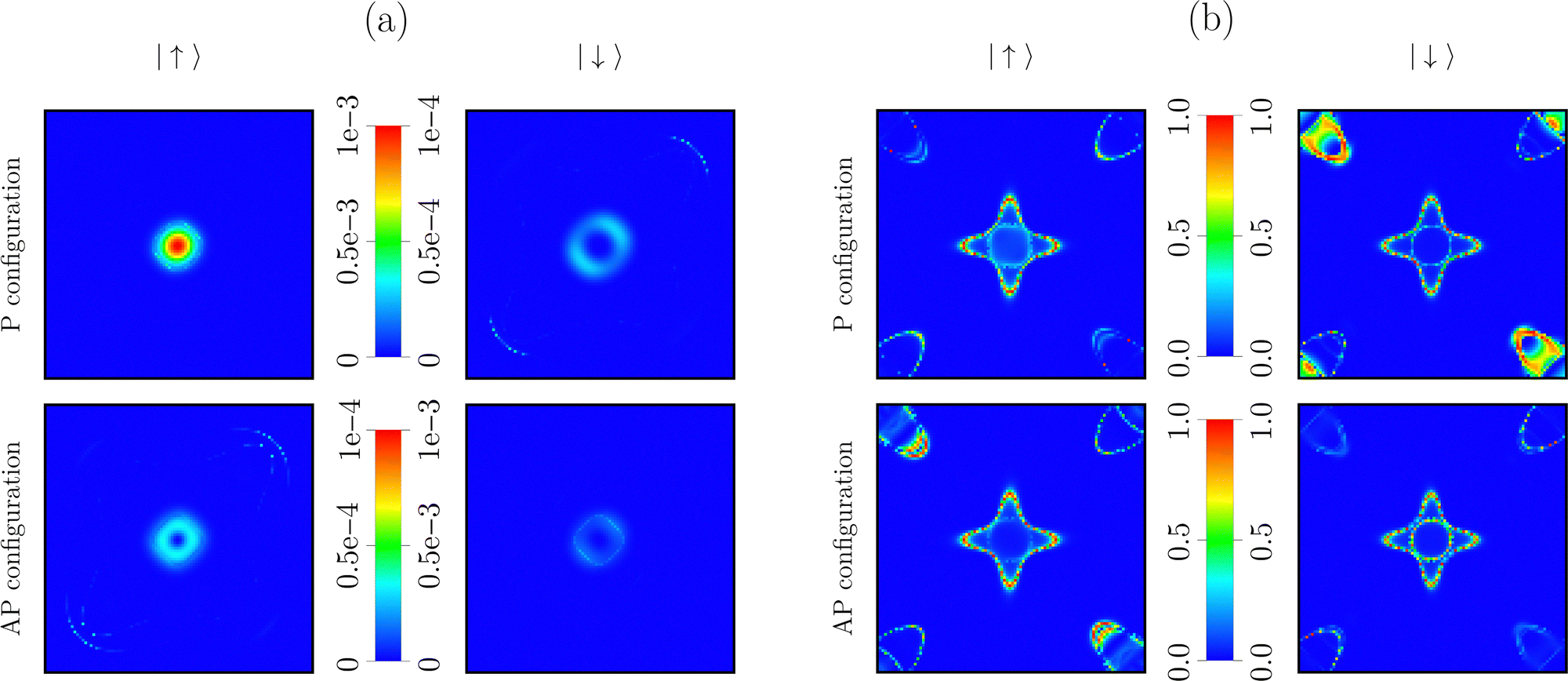 | ||
| Fig. 4 Zero bias transmission coefficient at EF for the (a) Fe/ZnSe/Fe and (b) Fe/ZnTe/Fe junctions plotted in the 2D BZ, i.e., as a function of k‖ = (kx, ky). Results are shown for the two spin channels and the P and AP configurations. | ||
E F of the Fe/ZnSe/Fe junction is close to midgap, i.e., the low bias transport is determined by electron tunneling and the symmetry-filtering argument comes into play. As a consequence, for both spin channels and magnetic configurations the maximal transmission is found around the Γ-point. Differences, however, emerge between the spin-dependent transmission functions. We consider first the P configuration and the majority spin channel. In this case the complex band of Δ1 symmetry determines the minimal κ (see Fig. 2(a)), i.e., the maximal transmission appears exactly at the Γ-point with a rapid decay away from the center of the 2D BZ. The band of Δ1 symmetry, however, is not available in the Fe band structure for the minority spin channel. Therefore, the transmission proceeds mainly through the bands of Δ2 and Δ5 symmetries, and the amplitude is maximal in an annular region around the Γ-point, but not exactly at the Γ-point, meaning that the tunneling electrons in the minority spin channel have a non-vanishing transverse wave vector. In addition, a minor contribution to the transmission (about 1% of the maximum) originates from two arc regions placed along the diagonal of the 2D BZ. Thus, the maximal transmission appears in an annular region around the Γ-point, with a minor contribution from the arc regions placed along the diagonal of the 2D BZ.
A different situation is encountered for the Fe/ZnTe/Fe junction. Here, EF lies just at the edge of the conduction band of ZnTe, i.e., the transport is not dominated by electron tunneling but by hopping conduction. As a consequence, the transmission coefficients approach unity and symmetry-filtering is no longer at play (being still at play away from EF, where electron tunneling takes place). The zero bias transmission maps in Fig. 4(b) indeed reveal significant amplitudes in different regions of the 2D BZ, particularly in a star-shaped region around the Γ-point and close to the corners.
Next, we analyze Tσ(E;V = 0) and the resulting TMR ratio as functions of the energy, which are plotted for both spin channels and magnetic configurations in Fig. 5. EF of the Fe/ZnSe/Fe junction lies close to the middle of the bandgap of ZnSe and the transport thus is tunneling-like. For the P configuration we notice that the transmission coefficient is larger for the majority spin channel than for the minority spin channel between −0.3 eV and 0.3 eV (EF = 0 eV). This is the region where the majority spin band with Δ1 symmetry of Fe overlaps with the complex band of minimal κ, which also has Δ1 symmetry. In the rest of the bandgap the tunneling current is carried by bands of Δ2 and Δ5 symmetries, resulting in a lower transmission. For E < −0.3 eV the minority spin current has a predominant Δ2 character and the majority spin current has a predominant Δ5 character. There is a resonant transmission peak near −0.3 eV, associated with a majority spin surface state. For the AP configuration, as expected, the transmission coefficient is almost spin-degenerate (not exactly, because the inversion symmetry is broken). We observe a strong energy dependence of the TMR ratio. Interestingly, we find that the TMR ratio at EF is about 200% and relatively constant within 0.4 eV around EF. This suggests that a large TMR ratio is realized in the typical bias range applied to MTJs. Note that our calculated TMR ratio is lower than what usually is found for the Fe/MgO/Fe junction with a barrier of similar thickness. This is due to the fact that the bandgap of ZnSe is significantly smaller than that of MgO, meaning that the wavefunction decay in ZnSe is slower than in MgO and the symmetry-filtering is less effective. Since symmetry-filtering is at play, one expects the TMR ratio to grow with the thickness of the tunnel barrier.
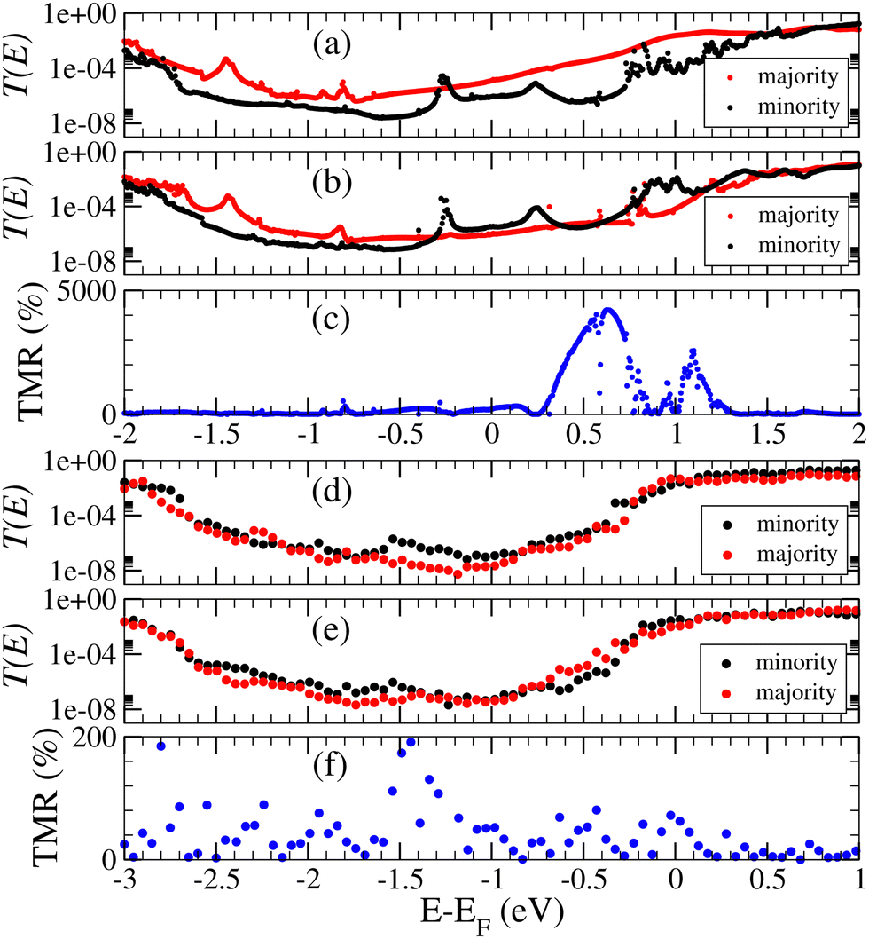 | ||
| Fig. 5 Total transmission coefficient of the Fe/ZnSe/Fe junction in the (a) P and (b) AP configurations and of the Fe/ZnTe/Fe junction in the (d) P and (e) AP configurations. For the AP configuration the spin quantization axis is set with respect to the right lead. Panels (c) and (f) show the energy dependence of the zero bias TMR ratio for the Fe/ZnSe/Fe and Fe/ZnTe/Fe junctions, respectively. | ||
According to Fig. 5(d), unfortunately, EF of the Fe/ZnTe/Fe junction is placed at the bottom of the conduction band of ZnTe, i.e., symmetry-filtering is not at play at EF. Therefore, the junction is similar to a standard giant magnetoresistance (GMR) spin valve and the zero bias GMR ratio is mainly determined by the spin polarisation of the leads. This results in a zero bias GMR of around 60%, which is a modest value. We expect this result to be rather robust, since the bottom of the conduction band is characterised by electrons with s symmetry, i.e., spin–orbit coupling is not at play. There is spin-filtering in the bandgap region, in particular for energies between −1 eV and −1.7 eV, where the transmission coefficient in the P configuration is dominated by the minority spin channel. This is associated with the band of Δ2 symmetry, which has its maximal dispersion in this energy window for the minority spin channel. The resulting TMR ratio for −1.7 eV < E < −1.0 eV touches 200%, but this is not accessible experimentally under normal bias.
IV. Conclusion
We have explored the potential of chalcogenide semiconductors as tunnel barriers in future MTJs. Specifically, we have studied ZnSe and ZnTe, which are extensively used in the solar cell and display industries, opening the possibility for integration in optical technologies. Our theoretical analysis, based on density functional theory and the non-equilibrium Green's functions method, relates the tunneling properties of the junctions to the electronic structures of the constituent compounds. In particular, we find for the Fe/ZnSe/Fe junction that the transport is tunneling-like, while in the case of the Fe/ZnTe/Fe junction EF is pinned to the conduction band of ZnTe and only a GMR effect with a modest GMR ratio of around 60% is achieved. In contrast, symmetry-filtering is at play in the case of the Fe/ZnSe/Fe junction, resulting in a TMR ratio of the order of 200% at EF, due to the predominant transmission of electrons with Δ1 symmetry, similar to the celebrated Fe/MgO/Fe platform. Unfortunately, since the bandgap of ZnSe is smaller than that of MgO, the TMR ratio never reaches very large values, but it is still useful for applications, particularly when considering that the current density achievable by this junction is large.Conflicts of interest
There are no conflicts to declare.Acknowledgements
The research reported in this publication was supported by funding from King Abdullah University of Science and Technology. SS thanks the Irish Research Council for financial support through the Advanced Laureate Award (IRCLA/2019/127).References
- D. B. Eason, Z. Yu, W. C. Hughes, W. H. Roland, C. Boney, J. W. Cook, J. F. Schetzina, G. Cantwell and W. C. Harsch, High-brightness blue and green light-emitting diodes, Appl. Phys. Lett., 1995, 66, 115 CrossRef CAS.
- N. A. Okerke and A. J. Ekpunobi, ZnSe buffer layer deposition for solar cell application, J. Non oxide Glasses, 2011, 3, 31 Search PubMed.
- Y. Chen, X. Mei, X. Liu, B. Wu, J. Yang, J. Yang, W. Xu, L. Hou, D. Qin and D. Wang, Solution-processed CdTe thin-film solar cells using ZnSe nanocrystal as a buffer layer, Appl. Sci., 2018, 8, 1195 CrossRef.
- G. Georgescu and A. Petries, Analysis of thickness influence on refractive index and absorption coefficient on zinc selenides thin films, Opt. Express, 2019, 27, 34803 CrossRef CAS PubMed.
- D. L. Rose, Eletron mobility in II-VI semiconductors, Phys. Rev. B: Solid State, 1970, 2, 10 Search PubMed.
- A. N. Krasnov, Y. F. Vaksman and Y. N. Purtov, p-Type condcutivity in ZnSe, J. Cryst. Growth, 1992, 123, 594 CrossRef CAS.
- A. P. Samantilleke, M. H. Boyle, J. Young and I. M. Dharmadasa, Growth of n-type and p-type ZnSe thin films using an electrochemical technique for applications in large area optoelectronics devices, J. Mater. Sci.: Mater. Electron., 1998, 9, 231 CrossRef CAS.
- J. H. Chang, T. Takai, B. H. Koo, J. S. Song, T. Handa and T. Yao, Aluminum-doped n-type ZnTe layers grown by molecular-beam epitaxy, Appl. Phys. Lett., 2001, 79, 785 CrossRef CAS.
- O. I. O. Olusola, M. L. Madugu and I. M. Dharmadasa, Growth of n- and p-type ZnTe semiconductors by intrinsic doping, Mater. Res. Innov., 2016, 19, 497 CrossRef.
- R. W. Robinson, Y. Han, H. Zhang, T. Ablekim, I. Khan, K. A. Persson and A. Zakutayev, Wide band gap chalcogenide semiconductors, Chem. Rev. B, 2020, 120, 4007 CrossRef PubMed.
- P. A. Berry, J. R. Macdonald, S. J. Beecher, S. A. McDaniel, K. L. Schepler and A. K. Kar, Fabrication and power scaling of a 1.7 W Cr:ZnSe waveguide laser, Opt. Mater. Express, 2013, 3, 1250 CrossRef.
- Y. Fang, Z. Yang, C. Li, P. Xu, K. Yan, Y. Sheng, H. Tao and R. Wang, Low loss and dispersion engineered ZnSe waveguides at telecom wavelengths, AIP Adv., 2021, 11, 065303 CrossRef CAS.
- Y. H. Cho, S. H. Park, W. G. Lee, J. H. Ha, H. S. Kim, N. Starzinskiy, D. H. Lee, S. Park and Y. K. Kim, Comparative study of a CsI and a ZnSe(Te/O) scintillation detector's properties for a gamma-ray measurement, J. Nucl. Sci. Technol., 2008, 5, 534 CrossRef.
- D. Linardatos, A. Konstantinidis, I. Valais, K. Ninos, N. Kalyvas, A. Bakas, I. Kandarakis, G. Fountos and C. Michail, On the optical response of tellurium activated zinc selenide ZnSe:Te single crystal, Crystals, 2020, 10, 961 CrossRef CAS.
- Handbook of Spin Transport and Magnetism, ed. E. Y. Tsymbal and I. Zutic, Chapman and Hall/CRC, Boca Raton, 2011 Search PubMed.
- S. Peng, Y. Zhang, M. Wang and W. Zhao, Magnetic tunnel junctions for spintronics: Principle and applications, Wiley, Hoboken, 2014, pp. 1–16 Search PubMed.
- J. M. D. Teresa, A. Barthelemy, A. Fert, J. P. Contour, F. Montaigne and P. Seneor, Role of metal-oxide interface in determining the spin polarization of magnetic tunnel junctions, Science, 1999, 286, 507 CrossRef PubMed.
- S. Bhatti, R. Sbiaa, A. Hirohata, H. Ohno, S. Fukami and S. N. Piramanayagam, Spintronics based random access memory: A review, Mater. Today, 2017, 20, 530 CrossRef.
- S. I. Kiselev, J. C. Sankey, I. N. Krivorotov, N. C. Emley, R. J. Schoelkopf, R. A. Buhrman and D. C. Ralph, Microwave oscillations of a nanomagnet driven by a spin polarized current, Nature, 2003, 425, 380 CrossRef CAS PubMed.
- J. Kaiser, W. A. Borders, K. Y. Camsari, S. Fukami, H. Ohno and S. Datta, Hardware-aware in-situ Boltzmann machine learning using stochastic magnetic tunnel junctions, Phys. Rev. Appl., 2022, 17, 014016 CrossRef CAS.
- F. A. Vincent, J. Larroque, N. Locatelli, N. R. Ben, O. Bichler, C. Gamrat, S. W. Zhao, J. Klein, S. R. Galdin and D. Querlioz, Spin-transfer torque magnetic memory as a stochastic memristive synapse for neuromorphic systems, IEEE Trans. Biomed. Circuits Syst., 2015, 9, 166 Search PubMed.
- G. Srinivasan, A. Sengupta and K. Roy, Magnetic tunnel junction based long-term short-term stochastic synapse for a spiking neural network with on-chip STDP learning, Sci. Rep., 2016, 6, 29545 CrossRef CAS PubMed.
- J. Toreejon, M. Riou, F. A. Arauujo, S. Tsunegi, G. Khalsa, D. Querlioz, P. Bortolotti, V. Cros, K. Yakushiji, A. Fukushima, H. Kubota, S. Yuasa, M. D. Stiles and J. Grollier, Neuromorphic computing with nanoscale spintronic oscillators, Nature, 2017, 547, 428 CrossRef PubMed.
- H. Cai, H. Y. Wang, L. Alves De Barros Naviner and W. Zhao, Robust ultra-low power non-volatile logic-in-memory circuits in FD-SOI technology, IEEE Trans. Cir. Sys. Regul. Pap., 2017, 64, 847 Search PubMed.
- K. Garello, F. Yasin and S. G. Kar, Spin–orbit torque MRAM for ultrafast embedded memories: From fundamentals to large scale technology integration, Proceedings of the 2019 IEEE 11th International Memory Workshop, Monterey, USA, 2019, pp. 1–4.
- Z. Wang, L. Zhang, M. Wang, Z. Wang, D. Zhu, Y. Zhang and W. Zhao, High-density NAND-like spin transfer torque memory with spin orbit torque erase operation, IEEE Electron Device Lett., 2018, 39, 343 CAS.
- L. Montesi, Z. Zilic, T. Hanyu and D. Suzuki, Building blocks to use in innovative non-volatile FPGA architecture based on MTJs, Proceedings of the 2012 IEEE computer society annual symposium on VLSI, Amherst, USA, 2012, pp. 302–307.
- S. A. Iyengar, S. Ghosh and J. Jang, MTJ-based state retentive flip-flop with enhanced-scan capability to sustain sudden power failure, IEEE Trans. Circuits Syst. Regul. Pap., 2015, 62, 2062 Search PubMed.
- H. Cai, Y. Wang, L. Alves De Barros Naviner and W. Zhao, Low power magnetic flip-flop optimization with FDSOI technology boost, IEEE Trans. Magn., 2016, 52, 3401807 Search PubMed.
- H. Meng, G. J. Wang and J. P. Wang, A spintronics full adder for magnetic CPU, IEEE Electron Device Lett., 2005, 26, 360 Search PubMed.
- H. Lee, C. Grezes, A. Lee, F. Ebrahimi, P. A. Khalili and L. K. Wang, A spintronic voltage-controlled stochastic oscillator for event-driven random sampling, IEEE Electron Device Lett., 2017, 38, 281 Search PubMed.
- C. E. Marques, N. Maciel, L. Naviner, H. Cai and J. Yang, A review of sparse recovery algorithms, IEEE Access, 2019, 7, 1300 Search PubMed.
- L. Berger, Emission of spin waves by a magnetic multilayer traversed by a current, Phys. Rev. B: Condens. Matter Mater. Phys., 1996, 54, 9353 CrossRef CAS PubMed.
- D. C. Ralph and M. D. Stiles, Spin transfer torques, J. Magn. Magn. Mater., 2008, 320, 1190 CrossRef CAS.
- K. Fujiwara, M. Oogane, A. Kanno, M. Imada, J. Jono, T. Terauchi, T. Okuno, Y. Aritomi, M. Morikawa, M. Tsuchida, N. Nakasato and Y. Ando, Magnetocardigraphy and magnetoencephalography measurements at room temperature using tunnel magneto-resistance sensors, Appl. Phys. Express, 2018, 11, 023001 CrossRef.
- Y. Jiang, Y. Lv, M. Jamali and J. Wang, Spin analog-to-digital converter using magnetic tunnel junction and spin Hall effect, IEEE Electron Device Lett., 2015, 36, 511 Search PubMed.
- A. Sengupta, M. C. Liyanagedera, B. Jung and K. Roy, Magnetic tunnel junction as an on-chip temperature sensor, Sci. Rep., 2017, 7, 11764 CrossRef PubMed.
- I. Chakraborty, A. Agrawal and K. Roy, Design of a low-voltage analog-to-digital converter using voltage-controlled stochastic switching of low barrier nanomagnets, IEEE Magn. Lett., 2018, 9, 3103905 Search PubMed.
- S. Salehi, B. M. Mashhadi, A. Zaeemzadeh, N. Rahnavard and F. R. DeMara, Energy-aware adaptive rate and resolution sampling of spectrally sparse signals leveraging VCMA-MTJ devices, IEEE J. Emerg. Sel. Top. Circuits Syst., 2018, 8, 679 Search PubMed.
- S. Salehi and F. R. DeMara, SLIM-ADC: Spin-based logic-in-memory analog to digital converter leveraging SHE-enabled domain wall motion devices, J. Microelectron., 2018, 81, 137 CrossRef.
- N. Maciel, E. Marques, L. Naviner, Y. Zhou and H. Cai, Magnetic tunnel junction applications, Sensors, 2020, 20, 121 CrossRef PubMed.
- C. Chappert, A. Fert and V. N. F. Dau, The emergence of spin electronics in data storage, Nat. Mater., 2007, 6, 813 CrossRef CAS PubMed.
- T. Miyazaki and N. Tezuka, Giant magnetic tunneling effect in Fe/Al 2 O 3/Fe junction, J. Magn. Magn. Mater., 1995, 139, L231 CrossRef CAS.
- J. S. Moodera, L. R. Kinder, T. M. Wong and R. Meservey, Large magnetoresistance at room temperature in ferromagnetic thin film tunnel junctions, Phys. Rev. Lett., 1995, 74, 3273 CrossRef CAS PubMed.
- M. Julliere, Tunneling between ferromagnetic films, Phys. Lett. A, 1975, 54, 225 CrossRef.
- I. I. Mazin, How to define and calculate the degree of spin polarization in ferromagnets, Phys. Rev. Lett., 1999, 83, 1427 CrossRef CAS.
- W. H. Butler, X. G. Zhang, T. C. Schulthess and J. M. Maclaren, Spin-dependent tunneling conductance of Fe/MgO/Fe sandwiches, Phys. Rev. B: Condens. Matter Mater. Phys., 2001, 63, 054416 CrossRef.
- J. Mathon and A. Umerski, Theory of tunneling magnetoresistance of an epitaxial Fe/MgO/Fe(001) junction, Phys. Rev. B: Condens. Matter Mater. Phys., 2001, 63, 220403 CrossRef.
- W. H. Butler, Tunneling magnetoresistance from a symmetry filtering effect, Sci. Technol. Adv. Mater., 2008, 9, 014106 CrossRef PubMed.
- G. Shukla, S. Sanvito and G. S. Lee, Fe and Co-based magnetic tunnel junctions with AlN and ZnO spacers, Phys. Rev. B, 2022, 105, 184427 CrossRef CAS.
- S. S. P. Parkin, C. Kaiser, A. Panchula, P. M. Rice, B. Hughes, M. Samant and S. H. Yang, Giant tunnelling magnetoresistance at room temperature with MgO (100) tunnel barriers, Nat. Mater., 2004, 3, 862 CrossRef CAS PubMed.
- S. Yuasa, T. Nagahama, A. Fukushima, Y. Suzuki and K. Ando, Giant room-temperature magnetoresistance in single-crystal Fe/MgO/Fe magnetic tunnel junctions, Nat. Mater., 2004, 3, 868 CrossRef CAS PubMed.
- J. M. MacLaren, W. H. Butler and X.-G. Zhang, Spin-dependent tunneling in epitaxial systems: Band dependence of conductance, J. Appl. Phys., 1998, 83, 6521 CrossRef CAS.
- J. M. Maclaren, X.-G. Zhang, W. H. Butler and X. Wang, Layer KKR approach to Bloch-wave transmission and reflection: Application to spin dependent tunneling, Phys. Rev. B: Condens. Matter Mater. Phys., 1999, 59, 5470 CrossRef CAS.
- P. Mavropoulos, N. Papanikolaou and P. H. Dederichs, Complex band structure and tunneling through Ferromagnet/Insulator/Ferromagnet junctions, Phys. Rev. Lett., 2000, 85, 1088 CrossRef CAS PubMed.
- F. Sacconi, J. M. Jancu, M. Povolotskyi and A. D. Carlo, Full-band tunneling in high-κ oxide MOS structures, IEEE Trans. Elec. Dev., 2007, 54, 3168 CAS.
- J. P. Velev, C. G. Duan, J. D. Burton, A. Smogunov, M. K. Niranjan, E. Tosatti, S. S. Jaswal and E. Y. Tsymbal, Magnetic tunnel junctions with ferroelectric barriers: Prediction of four resistance states from first principles, Nano Lett., 2009, 9, 427 CrossRef CAS PubMed.
- N. M. Caffrey, T. Archer, I. Rungger and S. Sanvito, Prediction of large bias-dependent magnetoresistance in all-oxide magnetic tunnel junctions with a ferroelectric barrier, Phys. Rev. B: Condens. Matter Mater. Phys., 2011, 83, 125409 CrossRef.
- H. X. Liu, Y. Honda, T. Taira, K. I. Matsuda, M. Arita, T. Uemura and M. Yamamoto, Giant tunneling magnetoresistance in epitaxial Co2 MnSi/MgO/Co2 MnSi magnetic tunnel junctions by half-metallicity of Co2 MnSi and coherent tunneling, Appl. Phys. Lett., 2012, 101, 132418 CrossRef.
- N. M. Caffrey, T. Archer, I. Rungger and S. Sanvito, Coexistance of giant tunneling electroresistance and magnetoresistance in an-all oxides magnetic tunnel junction, Phys. Rev. Lett., 2012, 109, 226803 CrossRef PubMed.
- N. M. Caffrey, D. Fritsch, T. Archer, S. Sanvito and C. Ederer, Spin-filtering efficiency of ferrimagnetic spinels CoFe2O4 and NiFe2O4, Phys. Rev. B: Condens. Matter Mater. Phys., 2013, 87, 024419 CrossRef.
- G. Shukla, T. Archer and S. Sanvito, HfO2 and SiO2 as barriers in magnetic tunneling junctions, Phys. Rev. B, 2017, 95, 184410 CrossRef.
- W. Zhao, E. Belhaire and C. Chappert, Spin-MTJ based Non-volatile flip-flop, Proceedings of 7th IEEE Conference on Nanotechnology, Hong Kong, China, 2007, pp. 399–402.
- A. Zarei and F. Safaei, Power and area-efficient design of VCMA-MRAM based full-adder using approximate computing for IoT applications, J. Microelectron., 2018, 82, 62 CrossRef.
- X. Jiang, A. F. Panchula and S. S. P. Parkin, Magnetic tunnel junctions with ZnSe barriers, Appl. Phys. Lett., 2003, 83, 5244 CrossRef CAS.
- H. C. Herper, P. Weinberger, A. Vernes, L. Szunyogh and C. Sommers, Electric transport in Fe/ZnSe/Fe heterostructures, Phys. Rev. B: Condens. Matter Mater. Phys., 2001, 64, 184442 CrossRef.
- D. M. Ceperly and B. J. Alder, Ground state of the electron gas by a stochastic method, Phys. Rev. Lett., 1980, 45, 566 CrossRef.
- J. M. Soler, E. Artacho, J. D. Gale, A. Garcia, J. Junquera, P. Ordejón and D. Sánchez-Portal, The SIESTA method for ab initio order N materials simulation, J. Phys.: Condens. Matter, 2002, 14, 2745 CrossRef CAS.
- C. D. Pemmaraju, T. Archer, D. Sánchez-Portal and S. Sanvito, Atomic-orbital-based approximate self-interaction correction scheme for molecules and solids, Phys. Rev. B: Condens. Matter Mater. Phys., 2007, 75, 045101 CrossRef.
- A. Filippetti, C. D. Pemmaraju, S. Sanvito, P. Delugas, D. Puggioni and V. Fiorentini, Variational pseudo-self-interaction-corrected density functional approach to the ab initio description of correlated solids and molecules, Phys. Rev. B: Condens. Matter Mater. Phys., 2011, 84, 195127 CrossRef.
- N. G. Szwacki, E. Przezdziecka, E. Dynowska, P. Boguslawski and J. Kossut, Structural properties of MnTe, ZnTe, and ZnMnTe, Acta Phys. Pol., A, 2004, 106, 233 CrossRef CAS.
- Q. Li, T.-T. Shen, Y.-L. Cao, K. Zhang, S.-S. Yan, Y.-F. Tian, S.-S. Kang, M.-W. Zhao, Y.-Y. Dai, Y.-X. Chen, G.-L. Liu, L.-M. Mei, X.-L. Wang and P. Grünberg, Spin memristive magnetic tunnel junctions with CoO-ZnO nano composite barrier, Sci. Rep., 2014, 4, 3835 CrossRef PubMed.
- M. M. Schwickert, J. R. Childress, R. E. Fontana, A. J. Kellock, P. M. Rice, M. K. Ho, T. J. Thompson and B. A. Gurney, Magnetic tunnel junctions with AlN and AlNxOy barriers, J. Appl. Phys., 2001, 89, 6871 CrossRef CAS.
- M. Althammer, E.-M. Karrer-Müller, S. T. B. Goennenwein, M. Opel and R. Gross, Spin transport and spin dephasing in zinc oxide, Appl. Phys. Lett., 2012, 101, 082404 CrossRef.
- A. R. Rocha, V. M. G. Suarez, S. Bailey, C. J. Lambert, J. Ferrer and S. Sanvito, Towards molecular spintronics, Nat. Mater., 2005, 4, 335 CrossRef CAS PubMed.
- A. R. Rocha, V. M. G. Suarez, S. Bailey, C. J. Lambert, J. Ferrer and S. Sanvito, Spin and molecular electronics in atomically generated orbital landscapes, Phys. Rev. B: Condens. Matter Mater. Phys., 2006, 73, 085414 CrossRef.
- I. Rungger and S. Sanvito, Algorithm for the construction of self-energies for electronic transport calculations based on singularity elimination and singular value decomposition, Phys. Rev. B: Condens. Matter Mater. Phys., 2008, 78, 035407 CrossRef.
- E. Bosoni and S. Sanvito, Complex band structure with nonn-orthogonal basis set: Analytical properties and implementation in the SIESTA code, J. Phys.: Condens. Matter, 2022, 34, 105501 CrossRef CAS PubMed.
| This journal is © the Owner Societies 2023 |