The influence of Fermi level position at the GaN surface on carrier transfer across the MAPbI3/GaN interface†
Received
20th February 2023
, Accepted 20th May 2023
First published on 25th May 2023
Abstract
Both gallium nitride (GaN) and hybrid organic–inorganic perovskites such as methylammonium lead iodide (MAPbI3) have significantly influenced modern optoelectronics. Both marked a new beginning in the development of important branches in the semiconductor industry. For GaN, it is solid-state lighting and high-power electronics, and for MAPbI3, it is photovoltaics. Today, both are widely incorporated as building blocks in solar cells, LEDs and photodetectors. Regarding multilayers, and thus multi-interfacial construction of such devices, an understanding of the physical phenomena governing electronic transport at the interfaces is relevant. In this study, we present the spectroscopic investigation of carrier transfer across the MAPbI3/GaN interface by contactless electroreflectance (CER) for n-type and p-type GaN. The effect of MAPbI3 on the Fermi level position at the GaN surface was determined which allowed us to draw conclusions about the electronic phenomena at the interface. Our results show that MAPbI3 shifts the surface Fermi level deeper inside the GaN bandgap. Regarding different surface Fermi level positions for n-type and p-type GaN, we explain this as carrier transfer from GaN to MAPbI3 for n-type GaN and in the opposite direction for p-type GaN. We extend our outcomes with a demonstration of a broadband and self-powered MAPbI3/GaN photodetector.
1 Introduction
Hybrid organic–inorganic perovskites (HOIPs) has become a hot topic in the field of semiconductor materials thanks to their outstanding optoelectronic properties1 and facile, low-cost synthesis predominantly based on wet-chemistry methods. The demonstration of the first HOIP based solar cell kicked off the race for higher power conversion efficiencies. In parallel to the efforts for achieving performance comparable to the standards set by conventional inorganic semiconductors (over 23%), the studies on light emitting diodes (LEDs), lasers and photodetectors emerged,2 which made perovskites an inseparable part of modern optoelectronics. Gallium nitride (GaN) being the most prominent representative of III–V semiconductors has been employed extensively and has remained one of the most significant semiconductors for decades now. It brought a breakthrough in solid state lighting3 and established a whole branch of high-power electronics.4 Nowadays, it also successfully acts as a reliable platform for tandem devices taking on board emerging materials such as van der Waals crystals and perovskites, which results in the demonstration of solar cells,5 LEDs,6,7 transistors8 and photodetectors.9,10 All presently proposed optoelectronic devices are multilayered, based on heterostructures with multiple interfaces.11 In this circumstance, the famous phrase “the interface is the device” evoked by H. Kroemer in his Nobel Lecture is as relevant as ever. Band alignment at the interfaces governs the device operation i.e. the energy barrier impacts the carrier dynamics and rules the carriers’ extraction or injection,12 which defines the device performance. In this context, it is clear that interface engineering is of great importance for the development of efficient optoelectronic devices. Since the subject of solar cell optimization is still dominating in the field of perovskite-based devices, the perovskite/metal,13 perovskite/charge transfer layer14 and perovskite/perovskite interfaces12 are extensively studied mostly using photoemission techniques such as X-ray photoelectron spectroscopy. In contrast to the scrupulous investigation of aforementioned cases and in the light of an increasing number of reported perovskite/GaN based devices, a systematic study providing an understanding of electronic phenomena at such interfaces is lacking.
The methodology proposed in this work provides direct access to the electronic phenomena at an interface. As was shown by our group, the interface in III–V based hybrid materials can be investigated through modulation spectroscopy, in particular contactless electroreflectance (CER). Through the analysis of the graphene/GaN and h-BN/GaN interface, we proved that CER is a powerful tool for carrier tracking in such a device.15,16 From the CER experiment, information about the surface barrier is extracted, which in turn enables us to conclude about charge carrier transport through the interface. Now, bearing in mind the significance of hybrid organic–inorganic perovskites, we direct our attention to CH3NH3PbI3 (MAPbI3), an indisputable game-changer in the field of materials for solar absorbers2,17 which has remained one of the most understood metal–halide perovskites for photovoltaics so far.
In this work, an MAPbI3/GaN interface is investigated via CER spectroscopy in order to address the carrier transfer across it. As a consequence, for the first time, the dependence of the direction of carrier flow through the MAPbI3/GaN interface on surface Fermi level positions in GaN is proposed. Additionally, a self-powered broadband MAPbI3/GaN-based photodetector is presented. According to our best knowledge, this is the first presentation of such a device in the given architecture.
2 Experimental
2.1 GaN substrates
To obtain sharp doping profiles, all samples in this study were grown by plasma-assisted molecular beam epitaxy on commercially available GaN/Al2O3 templates with an electron concentration of around 2 × 1018 cm−3. Standard effusion cells were used to provide the molecular beam of Ga and Si. To ensure low background doping, for Mg, a valved source for corrosive materials was used. Growth was carried out under metal-rich conditions with nitrogen supplied using a radio frequency Veeco plasma source set to 170 W and 8 sccm min−1 of N2 flow resulting in a growth rate of 0.33 mm h−1. Si and Mg doping concentrations were kept constant at 7 × 1018 cm−3 and 1 × 1019 cm−3, respectively. The as-grown GaN structures consisted of a 300 nm layer doped with Si or Mg followed by a 40–80 nm undoped part.
2.2 MAPbI3 film deposition
The CH3NH3PbI3 perovskite solution was prepared by dissolving powders of MAI and PbI2 in a molar ratio of 1![[thin space (1/6-em)]](https://www.rsc.org/images/entities/char_2009.gif) :1 in 9.0:1.1 (v/v) DMF/DMSO. Prior to MAPbI3 deposition, GaN substrates were treated with 15 wt% aqueous HCl solution, and they were cleaned by sonication in deionized water, acetone, and isopropyl alcohol (IPA) sequentially. Before layer processing, 60s of nitrogen plasma treatment was applied to remove organic residues. Immediately after, the substrates were transferred to a nitrogen-filled glovebox (H2O < 0.1 ppm; O2 <0.1 ppm). In order to provide sufficient wetting of the substrate, the GaN surface was illuminated using a UV lamp for 10 minutes (50 W, 365 nm) directly before MAPbI3 deposition. The perovskite layer was deposited following a two-step spin-coating procedure, using toluene as an antisolvent. Then, the sample was transferred to the hotplate for the annealing process, 10 min at 100 °C to evaporate the remaining solvents and the film then became darker.
:1 in 9.0:1.1 (v/v) DMF/DMSO. Prior to MAPbI3 deposition, GaN substrates were treated with 15 wt% aqueous HCl solution, and they were cleaned by sonication in deionized water, acetone, and isopropyl alcohol (IPA) sequentially. Before layer processing, 60s of nitrogen plasma treatment was applied to remove organic residues. Immediately after, the substrates were transferred to a nitrogen-filled glovebox (H2O < 0.1 ppm; O2 <0.1 ppm). In order to provide sufficient wetting of the substrate, the GaN surface was illuminated using a UV lamp for 10 minutes (50 W, 365 nm) directly before MAPbI3 deposition. The perovskite layer was deposited following a two-step spin-coating procedure, using toluene as an antisolvent. Then, the sample was transferred to the hotplate for the annealing process, 10 min at 100 °C to evaporate the remaining solvents and the film then became darker.
2.3 Photodetector fabrication
The undoped GaN layer was dry etched in the ICP-RIE plasma etcher with the BCl3/Cl2/Ar mixture from half of the surface of 1 × 1 cm GaN substrate to uncover the doped layer. Then, the MAPbI3 film was deposited on the unetched half. Silver electrical contacts were fabricated on GaN and MAPbI3 sites.
2.4 Structural and morphological characterization
A Park Systems Atomic Force Microscope (AFM) was employed for obtaining topographic images of MAPbI3 deposited onto the GaN surface. In XRD measurements, θ–2θ scans were performed using a Panalytical Empyrean diffractometer supported by a PIXcel3D detector and a planar goniometer. In the incidence X-ray beam path, a hybrid monochromator was used. This allows to achieve the divergence of the X-ray beam at the level of 12′′. A two-crystal analyzer was used in the diffracted beam path. For all the measurements, a αCuKα1 =1.540597 Å radiation source was used. The parameters of the X-ray tube were 40 mA and 40 kV.
2.5 Contactless electroreflectance
In the CER experiment, the reflectance and the modulated reflectance spectra are measured. In order to achieve this, the sample was illuminated by the laser-driven xenon lamp light dispersed through the 0.75 m Andor monochromator, while the external modulation by the AC voltage (3 kV, 280 Hz) is on. Light reflected by the sample is detected using a photomultiplier via the lock-in technique. The custom-made capacitor-like sample holder is used to mount a sample and to provide an electrical connection using a high voltage generator. More details regarding the experimental setup can be found elsewhere.18
2.6 Photocurrent measurements
The investigated sample was glued to the sapphire plate and mounted on the custom designed holder providing an electrical connection to the setup. Photocurrent measurements were performed in vacuum at room temperature under zero-bias conditions. The Stanford Research Systems SR570 preamplifier together with the SR830 lock-in was used to measure the signal. Power and time dependence was measured for 405 nm and 325 nm CW lasers illumination chopped by the mechanical chopper. The photocurrent time response was registered using a Rohde & Schwarz RTB2000 oscilloscope.
3 Results and discussion
3.1 Structures under study
15 nm thin MAPbI3 films were spin-coated on so-called van Hoof (vH) GaN structures.19Fig. 1 shows the design of an exemplary structure under study. vH GaN consists of a highly doped n-type (Si doping) or p-type (Mg doping) thick GaN layer covered with significantly thinner undoped GaN. For exact layers thickness, see the Materials and Methods section. As can be seen on the right-hand side of Fig. 1, knowing the thickness (d) and the value of the built-in electric field (F) of the undoped layer, the surface barrier Φ can be deduced. Such a direct sample architecture combined with possibilities offered by modulation spectroscopy provides a full picture of the electronic phenomena at the MAPbI3/GaN interface. An in-depth analysis of the benefits of this approach will be given in a section describing spectroscopic results.
 |
| | Fig. 1 Scheme of the MAPbI3/van Hoof GaN structure. On the left side of the picture perovskite structure is presented. On the right side, the conduction band bending for the Si doped structure is sketched. F, Φ, d denotes electric field, surface potential barrier and thickness of an undoped layer, respectively. | |
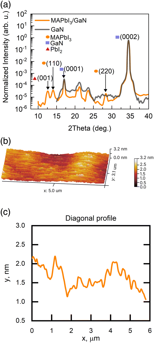
Fig. 2(a) shows the XRD spectra of reference GaN and MAPbI3/GaN structure. For bare GaN reflection (0002) is visible. For MAPbI3 containing samples, (110) and (220) peaks20 are detected confirming the presence of perovskite film on the GaN substrate.
 |
| | Fig. 2 (a) X-ray diffraction spectra of reference GaN and MAPbI3/GaN structure. (b) 3D AFM image of MAPbI3 film deposited on GaN van Hoof substrate. (c) Topography analysis of (b). | |
Fig. 2(b) and (c) present a 3D AFM image of perovskite film deposited on GaN and the diagonal profile across this layer, respectively. As can be seen, continuous, plain and smooth (RMS of 3.5 nm) MAPbI3 films, reproducing the roughness of GaN, were obtained.
3.2 Investigation of charge carrier behaviors at the MAPbI3/GaN interface
CER is a modulation spectroscopy technique shown to be an excellent tool for the investigation of built-in electric fields and electronic band structure of bulk materials and low dimensional structures.21 Recently, it was also proven that while adopting an appropriate methodology, CER results can provide information about the barrier height at the interface of two semiconductors enabling conclusions about the carrier transfer through it.15,16 In the CER experiment, the near-surface band bending is modulated by the alternating external electric field applied to the sample. As a consequence material's dielectric function is perturbed and relative changes in the reflectivity coefficient can be measured. For structures with the built-in electric field,19 the CER spectrum consists of resonance features visible at energies corresponding to direct optical transitions and Franz-Keldysh oscillations (FKO) arised at higher energies. The strength of this built-in electric field is linked to the FKO period and can be calculated through the following analysis. Eqn (1) describes the relationship between the FKO and built-in electric field:22| |  | (1) |
| |  | (2) |
where ℏθ is the electro-optic energy, Γ is the line width, φ is the phase, F is the electric field and μ is the electron–hole reduced mass for GaN. Eqn (3) defines FKO extrema:| | 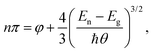 | (3) |
where En is the energy of each extremum and n is its index. The value of the electric field F can be calculated from the plot of (En−Eg)3/2versus n, which is a linear dependence with a slope proportional to F.
In order to fully benefit from the proposed methodology, samples with controlled built-in electric fields (van Hoof structures) were used as a platform for CER studies. At the doped/undoped layer interface, the Fermi level is close to the conduction band edge (CBE) or valence band edge (VBE) for n-type (Si) and p-type (Mg) doping, respectively. At the surface, the Fermi level is located at one of two existing GaN bandgap surface densities of states (SDOS) resulting mostly from Ga dangling bonds.23 Upper SDOS (US), stretching of about 0.6 eV from CBE into the GaN bandgap pins the surface Fermi level for n-doped structures. Lower SDOS (LS) is located about 1.7 eV from CBE, nearly in the middle of the GaN bandgap, and pins surface Fermi level for p-doped structures.24 Due to this difference in the Fermi level positions in bulk and at the surface, the electric field builds into the undoped layer and gives rise to the FKO in the CER spectrum. For n-type structures, surface barrier height can be extracted from the following relation between built-in electric field F and undoped layer thickness d:
For p-type structures, band bending and surface barrier can be obtained by solving the 1D Poisson equation.
24 Covering the vH GaN sample with MAPbI
3 affects the GaN surface states which in turn alters the built-in electric field, which is directly measured in CER. Through the analysis of the influence of MAPbI
3 on the Fermi level positions at the GaN surface, carrier transfer at the MAPbI
3/GaN interface can be explored.
In this study, a set of MAPbI3/GaN hybrids containing structures with 40, 60, 80 nm thick undoped GaN layers for n-type vH substrates and 60 nm for p-type vH were investigated. Fig. 3(a) and (b) show the CER spectra for reference GaN and MAPbI3/GaN structures for n-type and p-type vH, respectively. At each CER spectrum, a resonance related to GaN bandgap transition at the energy 3.43 eV is present with FKO (numbered) appearing above it. For each cap thickness, the period of FKO for MAPbI3-covered structures increases significantly compared to bare reference GaN. Such behavior points to the increase of built-in electric field for MAPbI3/GaN structures, which is consistent with the results of FKO period analysis done according to eqn (3) and presented in the insets of Fig. 3(a) and (b). The observed increase in the built-in electric field is related to the increase of barrier Φ for MAPbI3-covered structures. In order to extract exact Φ values for n-type vH substrates, built-in electric fields were fitted with eqn (4), see Fig. 3(c). For p-type vH structures, barrier Φ was calculated in NextNano solver according to the procedure described in ref. 24.
 |
| | Fig. 3 (a) CER spectra of reference n-type GaN and MAPbI3 covered van Hoof structures with 40, 60 and 80 nm thick undoped layers. Insets show the analysis of the built-in electric field. (b) CER spectra of reference p-type GaN and MAPbI3/GaN van Hoof sample with 60 nm undoped layer. Inset shows an analysis of the built-in electric field. (c) Determination of barrier Φ for structures presented in (a). Experimental uncertainties are smaller than the point's size. | |
Barriers determined for all the investigated samples are shown in Fig. 4(a). For reference GaN vH structures, barriers 0.32 eV and 1.13 eV were found for n-type (GaN:Si) and p-type (GaN:Mg), respectively. The scheme of the corresponding band bending is presented in Fig. 4(b) and (c). The obtained barriers are in line with literature reports.23,24 For MAPbI3-covered structures, barriers 0.85 eV (for n-type) and 1.60 eV (for p-type) were found. For further information about the influence of surface treatment prior to MAPbI3 deposition and MAPbI3 film thickness on the barrier Φ see the ESI.† Such an increase in Φ for MAPbI3-covered GaN can be translated into the surface Fermi level shift toward the middle of the GaN bandgap, which is schematically marked with a straight red arrow in Fig. 4(b) and (c). The observed increase in Φ correlated with surface Fermi level shift for MAPbI3 covered GaN is related to the carrier transfer through MAPbI3/GaN interface. The schematic representation of this process is shown in Fig. 4(b) and (c). Blue and orange areas represent GaN and MAPbI3 band alignment versus vacuum level, respectively. According to the literature, the CBE in GaN is located at the energy of about −3.25 eV,25 which is about 0.65 eV above the CBE in MAPbI3 (−3.9 eV26). For GaN surface with upward band bending, when the Fermi level is located on the US of surface states it lays above the MAPbI3 CBE, see Fig. 4(b). As a consequence, electrons from the GaN surface flow to MAPbI3 causing a downshift of Fermi level, which results in the increase of barrier (Φn). As it is shown in Fig. 4(c) for GaN surface with downward band bending (p-doped vH), when the Fermi level is located on the LS of surface states, it is below MAPbI3. As a consequence, the flow of carriers in the opposite direction is expected compared to the surface with upward band bending, namely carriers flow from MAPbI3 to GaN. This results in surface Fermi level up-shift and increase of surface barrier for holes (Φp). From Fig. 4(b) and (c) can be concluded that at the MAPbI3/GaN interface direction of carrier flow (MAPbI3 → GaN or GaN → MAPbI3) is determined by the surface Fermi level position at the GaN surface.
 |
| | Fig. 4 (a) Surface barrier height for GaN and MAPbI3/GaN structures. (b) Sketch of band bending for MAPbI3/n-GaN and (c) MAPbI3/p-GaN structure. Blue and orange areas symbolise GaN and MAPbI3 band alignment versus vacuum level. The straight red arrow indicates the MAPbI3 -induced shift of the surface Fermi level. The curved red arrow implies the direction of carrier transfer at the MAPbI3/GaN interface. | |
3.3 Self-powered MAPbI3/GaN photodetectors
In order to test the photoconversion capability of an investigated interface, we fabricated the simple photodetector based on MAPbI3/p-type vH GaN. Fig. 5(a) and (b) show a scheme and a picture of the device, respectively. As can be noticed, no additional carrier transport layers were introduced.
 |
| | Fig. 5 (a) Scheme of photodetector architecture. (b) Device photography. | |
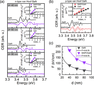
Fig. 6 shows the time-resolved photocurrent response of the device collected in two excitation regimes: at 325 nm and 405 nm, which is above GaN and MAPbI3 energy gap, respectively. As can be seen, the combination of these two materials with quite different bandgaps (GaN 3.4 eV vs. MAPbI3 1.55 eV) significantly extends the operation spectral range resulting in the broad band response spectrum for our device. Moreover, all presented results were obtained at zero bias conditions. Fig. 6(a) and (b) show stable photocurrent response obtained at 3 Hz modulation for 325 nm and 405 nm illumination at different powers (46 mW, 23 mW and 5 mW). Zoom of one period (at maximum power) extracted from panels (a) and (b) is presented in Fig. 6(c) and (d), respectively. The rise time (ton – counted from 10% to 90% of the maximum current) and fall time (toff – from 90% to 10% of the maximum current)27 are calculated for each illumination wavelength and depicted in the figures. Obtained rise times are 72 ms and 63 ms, while fall times are 62 ms and 110 ms for 325 nm and 405 nm, respectively. These values are superior to reports presented in refs. 28, 29 and comparable with ref. 27 Significantly longer fall time observed for 405 nm illumination may be ascribed to anomalous-like transient photocurrent behavior detected at below-GaN illumination regime. Such a shape of photocurrent has been already observed for organic part-containing semiconductors.30 Detailed analysis of this effect can be found in ref. 30.
 |
| | Fig. 6 (a) Power-dependent time-resolved photocurrent response under 325 nm and (b) 405 nm illumination. (c) Rise and decay time evaluation under 325 and (d) 405 nm illumination. | |
Photoresponsivity (R) and detectivity (D*), parameters describing device photo-electric conversion ability and sensitivity, respectively, are defined as31
| |  | (5) |
where
Iph is the photocurrent,
ρ is the illumination power density and
A is the illuminated area;
| |  | (6) |
where
q is the electronic charge constant and
Id is the dark current were calculated.
Fig. 7(a) and (b) shows R and D* at zero bias as a function of illumination intensity, respectively. As can be seen, both parameters decrease as illumination intensity increases. Significantly higher values of R and D* were obtained for 405 nm than for 325 nm illumination. It is consistent with previous observations for MAPbI3/GaN-based photodetectors29 indicating a good spectral selectivity of the device. Higher values of R are consistent with higher photocurrent obtained for longer wavelength excitation, which results from a greater absorption coefficient for MAPbI3 at 405 nm (2.9 × 105 cm−1) than for GaN at 325 nm (1.35 × 105 cm−1). Maximal obtained values of R and D* are 110 nA W−1 and 4.25 × 10¹¹ Jones, respectively. These numbers can be considered as decent, regarding the raw device architecture.
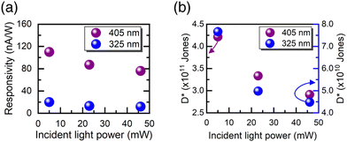 |
| | Fig. 7 (a) Power and spectral dependent photoresponsivity and (b) detectivity at zero bias. | |
4 Conclusions
In this work, the carrier transfer at an MAPbI3/GaN interface was investigated by CER spectroscopy – a noninvasive and reliable tool proven to be useful for contactless probing of electronic phenomena at a semiconductor interface. It was found that MAPbI3 spin-coated on GaN causes an increase in the surface barrier for carriers on the GaN surface. This is associated with the effect of unpinning of the surface Fermi level from its primary position. The identified underlying mechanism is the carrier transfer from the GaN surface to perovskite when the surface Fermi level in GaN is located on the upper singularity of surface states, for GaN with upward near surface band bending, what leads to the increase of surface barrier for electrons. In the case when the surface Fermi level in GaN is located on the lower singularity of surface states, for GaN with downward near surface band bending, the opposite carrier flow takes place: from MAPbI3 to GaN, what increases the surface barrier for holes. This points to the conclusion that the direction of carrier transfer through the MAPbI3/GaN interface depends on the Fermi level pinning at the GaN surface. Additionally, by fabrication of a photodetector based on the investigated MAPbI3/GaN interface, it was shown that without optimization and additional carrier transport layers, it exhibits a stable, broadband and fast operation performance in the self-powered mode.
Author contributions
E.Z. – Investigation, formal analysis, writing – original draft, and project administration; A. P. H. – validation and writing – review & editing; Ł. P. – resources and investigation; K. O. – investigation; J. S. - investigation; M. C. – resources and investigation; C. S. – resources and supervision; R. K. – conceptualization and supervision.
Conflicts of interest
There are no conflicts to declare.
Acknowledgements
This work was supported by the National Science Centre (NCN) in Poland through OPUS grant no. 2019/35/B/ST5/02819 and no. UMO-2019/33/B/ST3/03021.
References
- A. M. Ganose, C. N. Savory and D. O. Scanlon, Chem. Commun., 2017, 53, 20–44 RSC.
- Y.-T. Li, L. Han, H. Liu, K. Sun, D. Luo, X.-L. Guo, D.-L. Yu and T.-L. Ren, ACS Appl. Electron. Mater., 2022, 4, 547–567 CrossRef CAS.
- S. Nakamura, T. Mukai and M. Senoh, Appl. Phys. Lett., 1994, 64, 1687–1689 CrossRef CAS.
- E. A. Jones, F. F. Wang and D. Costinett, IEEE J. Emerg. Sel. Top. Power Electron., 2016, 4, 707–719 Search PubMed.
- K. J. Lee, J.-W. Min, B. Turedi, A. Y. Alsalloum, J.-H. Min, Y. J. Kim, Y. J. Yoo, S. Oh, N. Cho, R. C. Subedi, S. Mitra, S. E. Yoon, J. H. Kim, K. Park, T.-H. Chung, S. H. Jung, J. H. Baek, Y. M. Song, I. S. Roqan, T. K. Ng, B. S. Ooi and O. M. Bakr, ACS Energy Lett., 2020, 5, 3295–3303 CrossRef CAS.
- Z.-T. Li, H.-W. Zhang, J.-S. Li, K. Cao, Z. Chen, L. Xu, X.-R. Ding, B.-H. Yu, Y. Tang, J.-Z. Ou, H.-C. Kuo and H.-L. Yip, Adv. Sci., 2022, 9, 2201844 CrossRef CAS PubMed.
- A. K. Singh, K. Ahn, D. Yoo, S. Lee, A. Ali, G.-C. Yi and K. Chung, NPG Asia Mater., 2022, 14, 57 CrossRef CAS.
- A. Zubair, A. Nourbakhsh, J.-Y. Hong, M. Qi, Y. Song, D. Jena, J. Kong, M. Dresselhaus and T. Palacios, Nano Lett., 2017, 17, 3089–3096 CrossRef CAS PubMed.
- Y. Zheng, B. Cao, X. Tang, Q. Wu, W. Wang and G. Li, ACS Nano, 2022, 16, 2798–2810 CrossRef CAS PubMed.
- X. Tang, Y. Zheng, B. Cao, Q. Wu, J. Liang, W. Wang and G. Li, ACS Appl. Nano Mater., 2022, 5, 4515–4523 CrossRef CAS.
- X. Xu and X. Wang, Small Struct., 2020, 1, 2000009 CrossRef.
- D. Luo, X. Li, A. Dumont, H. Yu and Z.-H. Lu, Adv. Mater., 2021, 33, 2006004 CrossRef CAS PubMed.
- F. Zu, D. Shin and N. Koch, Mater. Horiz., 2022, 9, 17–24 RSC.
- F. Zu, P. Amsalem, M. Ralaiarisoa, T. Schultz, R. Schlesinger and N. Koch, ACS Appl. Mater. Interfaces, 2017, 9, 41546–41552 CrossRef CAS PubMed.
- A. P. Herman, L. Janicki, H. S. Stokowski, M. Rudzinski, E. Rozbiegala, M. Sobanska, Z. R. Zytkiewicz and R. Kudrawiec, Adv. Mater. Interfaces, 2020, 7, 2001220 CrossRef CAS.
- E. Zdanowicz, A. P. Herman, K. Opołczyńska, S. Gorantla, W. Olszewski, J. Serafińczuk, D. Hommel and R. Kudrawiec, ACS Appl. Mater. Interfaces, 2022, 14, 6131–6137 CrossRef CAS PubMed.
- L. Mao, C. C. Stoumpos and M. G. Kanatzidis, J. Am. Chem. Soc., 2019, 141, 1171–1190 CrossRef CAS PubMed.
- E. Zdanowicz, A. P. Herman and R. Kudrawiec, Appl. Surf. Sci., 2022, 577, 151905 CrossRef CAS.
- C. V. Hoof, K. Deneffe, J. D. Boeck, D. J. Arent and G. Borghs, Appl. Phys. Lett., 1989, 54, 608–610 CrossRef.
- A. Marronnier, H. Lee, H. Lee, M. Kim, C. Eypert, J.-P. Gaston, G. Roma, D. Tondelier, B. Geffroy and Y. Bonnassieux, Solar Energy Mater. Solar Cells, 2018, 178, 179–185 CrossRef CAS.
- R. Kudrawiec, Phys. Status Solidi B, 2010, 247, 1616–1621 CrossRef CAS.
- D. E. Aspnes and A. A. Studna, Phys. Rev. B, 1973, 7, 4605–4625 CrossRef CAS.
- C. G. Van de Walle and D. Segev, J. Appl. Phys., 2007, 101, 081704 CrossRef.
- Ł. Janicki, M. Gładysiewicz, J. Misiewicz, K. Klosek, M. Sobanska, P. Kempisty, Z. R. Zytkiewicz and R. Kudrawiec, Appl. Surf. Sci., 2017, 396, 1657–1666 CrossRef.
- Z. Zhang, Q. Qian, B. Li and K. J. Chen, ACS Appl. Mater. Interfaces, 2018, 10, 17419–17426 CrossRef CAS PubMed.
- P. Wangyang, C. Gong, G. Rao, K. Hu, X. Wang, C. Yan, L. Dai, C. Wu and J. Xiong, Adv. Opt. Mater., 2018, 6, 1701302 CrossRef.
- S. Mitra, M. M. Muhammed, N. Alwadai, D. R. Almalawi, B. Xin, Y. Pak and I. S. Roqan, RSC Adv., 2020, 10, 6092–6097 RSC.
- Q. Li, G. Liu, J. Yu, G. Wang, S. Wang, T. Cheng, C. Chen, L. Liu, J.-Y. Yang, X. Xu and L. Zhang, J. Mater. Chem. C, 2022, 10, 8321–8328 RSC.
- H. Zhou, J. Mei, M. Xue, Z. Song and H. Wang, J. Phys. Chem. C, 2017, 121, 21541–21545 CrossRef CAS.
- L. Hu, X. Liu, S. Dalgleish, M. M. Matsushita, H. Yoshikawa and K. Awaga, J. Mater. Chem. C, 2015, 3, 5122–5135 RSC.
- C. Zou, Q. Liu, K. Chen, F. Chen, Z. Zhao, Y. Cao, C. Deng, X. Wang, X. Li, S. Zhan, F. Gao and S. Li, Mater. Horiz., 2022, 9, 1479–1488 RSC.
Footnote |
| † Electronic supplementary information (ESI) available: Information about the influence of surface treatment prior to MAPbI3 deposition and MAPbI3 film thickness on the surface barrier. See DOI: https://doi.org/10.1039/d3cp00801k |
|
| This journal is © the Owner Societies 2023 |
Click here to see how this site uses Cookies. View our privacy policy here. 
 Open Access Article
 This Open Access Article is licensed under a Creative Commons Attribution-Non Commercial 3.0 Unported Licence
 *a,
Artur P.
Herman
*a,
Artur P.
Herman