
 Open Access Article
 This Open Access Article is licensed under a Creative Commons Attribution-Non Commercial 3.0 Unported Licence
Bridging the gas and condensed phases for metal-atom encapsulating silicon- and germanium-cage superatoms: electrical properties of assembled superatoms†
Takaho
Yokoyama
 and
Atsushi
Nakajima
*
and
Atsushi
Nakajima
*
Department of Chemistry, Faculty of Science and Technology, Keio University, 3-14-1 Hiyoshi, Kohoku-ku, Yokohama 223-8522, Japan. E-mail: nakajima@chem.keio.ac.jp; Fax: +81-45-566-1697; Tel: +81-45-566-1712
First published on 3rd March 2023
Abstract
With the development of nanocluster (NC) synthesis methods in the gas phase, atomically precise NCs composed of a finite number of metal and semiconductor atoms have emerged. NCs are expected to be the smallest units for nanomaterials with various functions, such as catalysts, optoelectronic materials, and electromagnetic devices. The exploration of a stable NC called a magic number NC has revealed a couple of important factors, such as a highly symmetric geometric structure and an electronic shell closure, and a magic number behavior is often enhanced by mixing additional elements. A synergetic effect between geometric and electronic structures leads to the formation of chemically robust NC units called superatoms (SAs), which act as individual units assembled as thin films. The agglomeration of non-ligated bare SAs is desirable in fabricating the assembled SAs associated with intrinsic SA nature. The recent development of an intensive pulsed magnetron sputtering method opens up the scalable synthesis of SAs in the gas phase, enabling the fabrication of SA assembly coupled with the non-destructive deposition of a soft-landing technique. This perspective describes our recent progress in the investigation of the formation of binary cage SA (BCSA) assembled thin films composed of metal-atom encapsulating silicon-cage SAs (M@Si16) and germanium-cage SAs (M@Ge16), with a focus on their electrical properties associated with a conduction mechanism toward the development of new functional nanoscale materials.
1. Introduction
Nanoscale materials have attracted considerable attention owing to their potential for the miniaturization of various devices and their novel functionalities. Some examples include quantum dots, two-dimensional (2D) nanosheets, and nanotubes. Among which, atomically precise nanoclusters (NCs) composed of a finite number of atoms are one of the most interesting nanomaterials possessing unique properties that strongly depend on size and composition. Given that the physical and chemical properties of NCs differ from those of bulk states despite the same constituent elements, a suitable choice of size and composition is the key for desirable functionality. The novelty of NCs is represented by the terms “small is different,”1,2 “every atom counts,”3 or “a new kind of alchemy,”4 implying that NCs can be regarded as novel building blocks in addition to elements in a periodic table.For the application of NCs as nanoscale materials, the realization of designer NC assembly in a well-controlled manner is a promising methodology that faces two general challenges. One is the large-scale synthesis of NCs for the preparation of specimens in practical time, and the other is the technique to deposit NCs without severe rearrangement such as the deformation and coalescence of NCs. In these contexts, one symbolic goal in NC research is the fabrication of condensed matter based on atomically precise NCs as building blocks, namely, the realization of “cluster-assembled materials”. The physics of cluster-assembled materials was first argued theoretically by Khanna and Jena, posing the question of whether the condensed phase of atomic NCs can retain their structure.5,6 In their early theoretical investigation, they found that NCs with high stability that simultaneously fulfilled the highly symmetric geometric structure and closed electronic shell would retain their units as experimentally demonstrated by the building blocks of B@Al12−.7 Stable NCs can be viewed as atom-mimicking particles that provide a third dimension to the periodic table and they have been conceptualized as superatoms (SAs). The fabrication of NC assemblies has also claimed the importance of the mass production of atomically precise NCs to experimentally verify how the crystal structure and electronic states evolve from single NCs to the assembled states.
In NC research, the development of novel experimental set-ups, particularly NC sources and high sensitive detection, is crucial for exploring the fundamental properties of NCs.8 Hence, novel NC generation methods developed in the gas phase to increase the NC amounts and techniques for the intact deposition of NCs on surfaces have been established.9,10
One of the ways to obtain a large amount of NCs is to allow size distributions without atomic precision; nanoparticles often exhibit size-dependent characteristics which are not scalable by their bulk counterparts. These novel size-dependent physical phenomena can also be observed in cluster-assembled films fabricated by gas phase beam deposition but cannot be found in simple atom deposition.11,12 For example, cluster-beam deposited films can work as neuromorphic devices through stable and reproducible resistive switching behaviors.13,14 The potential applications of cluster-assembled systems include gas sensors,15,16 tunable band gap materials,17 and plasmonic materials.18
For the sophisticated characteristics of NC assembled materials, cluster assemblies must be formed through atomically precise size selection requiring a high intensity NC source. We recently developed the source of nanojima®, combined with soft landing apparatus,19 which allows us to prepare non-ligated bare NCs as a NC beam with a wide choice of elements and their mixture in scalable amounts. A NC ion beam must be generated with well-controlled kinetic energy because a beam with narrowly distributed kinetic energies achieves a low collision energy when NC ions collide with the substrate, which is called “soft-landing” and allows deposition on the surface without decomposition and implantation.20,21 The NC source enables us to fabricate NC-deposited substrates applicable as catalysts,22–25 plasmonic sensitizers,26 and optoelectronic materials27 and have a deep understanding of cluster–surface interaction with organic substrates.28–30 In addition, the NC source can be modified to obtain NC solutions31 and NC-deposited powders.32 The methods are called direct liquid/powder embedded trapping (DiLET/DiPET),31,32 opening an opportunity to investigate the properties of bare NCs in various environments. What is more is the fabrication of assembled films and characterization of macroscopic properties such as electrical conduction.33 The advanced setup for the size-selective NC deposition has realized NC assembly into a solid agglomeration composed of gas phase synthesized bare NCs.
NCs with high symmetric geometry and atom-mimicking properties can be viewed as robust superatoms (SAs). Certain NCs with adequate size and elemental composition make their electronic structure similar to that of atoms in the periodic table.6,34,35 Like atoms form an electronic shell composed of atomic orbitals of s, p, d, f,… SAs have resembled orbitals called superatomic orbitals that are delocalized to overall SA denoted as S, P, D, F,… with capital letters representing the angular momentum of the superatomic orbitals. The concept of SAs can explain various features of SAs in terms of the electronic shell model. For instance, SAs with a total valence electron number corresponding to shell closure can be regarded as rare gas-like SAs. The emergent superatomic periodicity suggests that certain classes of NCs can be considered as constituents of a three-dimensional periodic table. The superatomic periodicity in assembled systems must be revealed, particularly for non-ligated SAs toward the realization of cluster-assembled materials to achieve the collective macroscopic properties through the direct accumulation of each SA. An optimized mixing ratio of constituent atoms with expected synergistic effects between geometric and electronic features is crucial to realize SAs as robust building blocks not with aggregation but with agglomeration; a representative SA can be exemplified by one central-atom encapsulated in a cage structure, i.e., an endohedrally doped cage completing a binary cage SA (BCSA). BCSAs typically exhibit robustness arising from the simultaneous satisfaction of geometric packing and electronic shell closures. This synergetic effect of the stabilization allows BCSAs to form a series of family constituting systematic and periodic chemistry. The electron number of BCSAs can be tuned one by one under the same skeleton structure by replacing the central metal atom just like the periodicity in the conventional periodic table of elements.36 Among various BCSAs (including Al based X@Al12 and endohedral fullerene (M@Cn)),37 metal-atom encapsulating silicon cage BCSAs (M@Si16) are promising candidates for SA assembly because the substitution of the central metal-atom enables the design of electronic properties36 and their structural robustness retains their unique caged structure even when assembled.28 Various kinds of transition- and lanthanide-metal (M) can be encapsulated in Si16 cages, rendering the M@Si16 family tailor-made agglomerated materials based on superatomic periodicity.38 Furthermore, cage atoms can be altered from Si to Ge, enabling the tuning of cage properties.39,40 Since our recent achievement in the electrical characterization of M@Si16 assembled films with group-5 metal-atom encapsulation (M = V, Nb, and Ta),33 we extended the characterization with different group metals and with Ge cage BCSAs to widen the perspective on M@Si16/M@Ge16 SA-assembled films.
In this perspective, we describe BCSA-based material characterization starting from the gas phase study (Section 2), followed by a surface immobilized system (Section 3) and finally assembled systems (Section 4). In particular, we highlight M@Si16 and M@Ge16 BCSAs as promising examples for naked SA assembled systems from gas phase synthesis.
2. Nanoclusters synthesized in the gas phase
This section briefly summarizes some basics of gas phase synthesized NCs, including M@Si16/M@Ge16 in an isolated system. The characterization of NCs in the gas phase is ideal for extracting the intrinsic size effect of stability, reactivity, and structure of naked NCs owing to negligible interaction with outer environments. A specific size that possesses the remarkable stability of NCs in the mass spectrometry appears as a magic number due to geometrical packing and/or electronic shell closures. Selective generation such as M@Si16/M@Ge16 BCSAs occurs at a specific charge state. Given that each Si atom possess 4 valence electrons, 68 electron shell closures of the superatomic orbitals of (1S)2(1P)6(1D)10(1F)14(2S)2(1G)18(2P)6(2D)10 is achieved when 4 additional electrons are shared by an M atom including a charge state. Owing to 68 electron shell closures, a stable charge state can be modified by the group of central metal atoms as shown in Fig. 1, allowing M@Si16/M@Ge16 BCSAs to resemble the case of atoms in the periodic table and they are regarded as building blocks in the superatomic periodicity; group 4 metal-atom (M) encapsulation with the 4 additional valence electrons can be viewed as a rare gas-like SA of neutral M@Si16/M@Ge16.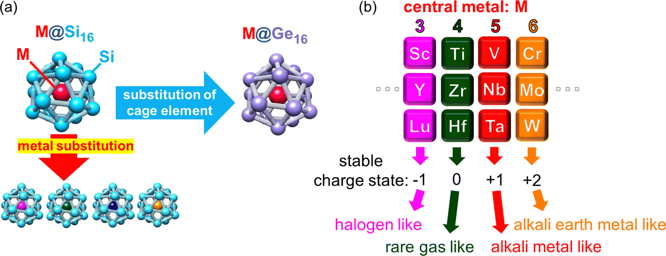 | ||
| Fig. 1 Overview of M@Si16 and M@Ge16 SAs. (a) Geometric structure of M@Si16 with metal substitution and cage element substitution into M@Ge16. (b) Transition metal to be encapsulated and the corresponding superatomic nature of M@Si16 and M@Ge16. | ||
When an M of another group is encapsulated, the cationic and anionic charge states would be compensated to satisfy 68 electrons, creating superatomic behavior as shown in Fig. 1(b); group-3, -4, -5, and -6 metal-atom encapsulation generates M@Si16/M@Ge16 halogen-like, rare gas-like, alkali metal-like, and alkali earth metal-like BCSAs, respectively. Chemical reactivity between BCSAs and molecules can be rationalized by their geometric/electronic structures, allowing the geometrical and electronic evaluation of the size evolution. In the following section, previous studies in the gas phase and theoretical calculation of M@Si16/M@Ge16 BCSAs and experimental set-ups for gas phase NC generation and basic principles for magic number behavior are summarized. Readers can also refer to recent reviews of M@Si16 and other kinds of endohedrally doped clusters.36,37,41
2.1 Set-ups for NC generation in the gas phase
Substantial progress has been achieved in the exploration of small sized atomically precise NCs owing to the development of the molecular beam technique. Molecular clusters and van der Waals clusters with weak interaction have been generated by gas condensation in a supersonic jet with low temperature. For example, xenon NCs (Xen) are formed by the adiabatic expansion of Xe atoms through a capillary into a vacuum and found to be abundant at specific sizes such as n = 13, 55, and 147 corresponding to the size required for the closed icosahedral structure, indicating that rather than an electronic factor, a geometric factor is important for the stability of Xen.42For NCs composed of metallic elements and metalloids, the three principal types of generation methods are gas evaporation, laser vaporization, and sputtering method. In gas evaporation, metal solids are evaporated in an oven placed in a vacuum chamber, and metal atoms are cooled by supersonic expansion to aggregate into NCs. Although this method allows the generation of large sized NCs with high intensity, applicable elements are restricted to highly volatile elements, such as alkali metals,43,44 mercury (Hg),45 antimony (Sb), bismuth (Bi), and lead (Pb).46
Laser vaporization is a versatile method to accelerate NC research and was developed independently by Smalley47 and Bondybey.48 A rod or disk composed of the target element is ablated by a collimated laser pulse so that the generated atoms and ions follow the clustering by cooling carrier gas. Not only metal elements but also non-metal elements can be applied. With the use of two lasers, binary NCs including BCSAs with high tunability of composition can further be achieved by controlling the timing and laser power of two lasers.49,50 Face-to-face configuration of two targets with the focusing point of the laser close to each rod leads to the effective mixing of two components in hot plasma, resulting in the highly efficient generation of binary NCs.51
Sputtering is an alternative method for NC generation where atoms and ions are generated by collisions of ionized rare gas atoms, such as argon cation (Ar+) and Xe+, into a target. Although the phenomenon of sputtering itself was discovered in the middle of the 19th century, the first attempt at utilizing sputtering in NC synthesis was conducted by Haberland and coworkers.52 Given that a magnet gives the plasma higher density, magnetron sputtering (MSP) has been widely used. When the sputtering gas is generated by a high energetic source,53,54 NC ions are generated at the sputtering event. With adequate cooling against exothermic clustering,55,56 the generated atoms and atomic ions grow into NCs. Multi elemental NCs can be synthesized using a mixed target or positioning multiple magnetron sputtering sources.16,36 An efficient way to enhance the ion ratio is to use pulsed discharge57 of high power impulse magnetron sputtering (HiPIMS), where the peak power can be increased compared with direct current (DC) sputtering compensated by a low duty cycle.58
Our group developed a high intensity NC beam source “nanojima®” based on HiPIMS coupled with a gas flow cell reactor for NC growth and size selection by a quadrupole mass spectrometer.19 Pulsed discharge generates a bunch composed of atoms and ions that condense into NCs, where NC generation can be optimized by the peak power of the pulse voltage and repetition rate. Time resolved evaluation revealed that increasing the peak power leads to a high density of atoms and ions and increasing the repetition rate results in the overlap of bunches.59 The NC formation mechanism can be explained by an extended Smoluchowski model where attractive interactions between NC cations and anions explain the origin of the size tuning.60 Coupled with an octupole ion guide, ion deflector, and quadrupole mass filter, the size-selected NC ions can be generated at high intensity of typically more than 1 nA. Given that the internal energy of NCs generated by MSP is lower than that generated by laser vaporization, the narrow kinetic energy distributions of the NC beam can be achieved for the non-destructive deposition of soft landing onto a substrate.
2.2 Effect of the geometric and electronic structure on the stability of NCs
The exploration of stable NCs was the initial interest in NC research and has been discovered in high abundance in mass spectra and by chemical tolerance toward etching gas. The stability of NCs can be discussed in two major factors: geometric and electronic structures. Atoms in NCs tend to organize to minimize the surface energy and quench dangling bonds, which is favorable in a closely packed structure such as icosahedral and decahedral structures. Several electron counting rules were proposed to account for the stabilization by an electronic factor: three major rules of (1) 18 electron rule, (2) Wade–Mingos rule, and (3) jellium model assuming spherical potential. The 18 electron rule was initially proposed in organometallic compounds, where metal-atom satisfies 18 electrons with d10s2p6 closure.61 For example, W@Au12 and Mo@Au12 satisfy 18 electrons with 6 electrons of W or Mo and 12 electrons from Au12 with each Au possessing 1 electron.62 The Wade–Mingos rule is applicable to polyhedral structures and their correlation between the number of valence electrons,63,64 which explains the stability, structure, and the bonding patterns of various types of Zintl clusters.65The spherical jellium model is applicable for a wide variety of NCs with near spherical shape, where valence electrons are assumed to be delocalized over the NCs within a uniformly positively charged sphere.66 Magic numbers of Nan NCs coincide with the number of electrons required to fill the shell, n = 8, 20, 40, 58, and 92.67 Another example is the photoelectron spectra of magnesium NC anions (Mgn−) showing wide electronic gaps at n = 4, 10, 20, and 35, corresponding to 8, 20, 40, and 70 electron shell closures, respectively.68 For Al NCs, 3 valence electrons are donated by each Al atom to the superatomic orbitals. Therefore, magic numbers appear when total valence electrons including a charge state match with the number required for closed electronic shells, such as Al7+, Al13−, and Al23−.69 Magic number behaviors can also be satisfied by mixing two elements. When Al NCs are mixed with a Na atom, Al13Na completes the 40 electron shell closure as revealed by its higher ionization potential compared with that of Al13.70 Mg possesses 2 electrons, resulting in the high stability of Al5Mg2− and Al11Mg3− corresponding to 20 and 40 electron shell closures.71 Although electron counting is a delicate issue to consider how many valence electrons are shared by each atom, endohedral geometry seems to favor the delocalization of 3d electrons metal doped silver (Ag) NCs.72 In addition to the geometrical closely packed structure, the number of total valence electrons and electron counting rules should be appropriately chosen for each system to discuss the electronic states of NCs.
2.3 Findings of M@Si16/M@Ge16 and their superatomic nature
The magic number behaviors in metal–Si NCs were discovered by Beck in the late 1980s, revealing that when a group 6 metal-atom of Cr, Mo, and W is mixed with Si atoms, cationic M@Si15 and M@Si16 are dominantly generated despite the predominant formation of pure Sin NCs below n = 11.73,74 Given that pure Sin NCs are chemically unstable owing to Si dangling bonds, metal-atom doping can effectively quench the unstable dangling bonds. Metal-atom encapsulation in a Si16 cage was experimentally confirmed by using a chemical probe method. H2O vapor was exposed to MSin NCs with various sizes in the gas phase.75,76 Given that H2O adsorption for a metal-atom more readily occurs compared with that for Si atoms, metal-atom encapsulation can be identified by the size where the adsorption reaction rate drops. Thereafter, theoretical calculations of group-4 metal-atom (Ti, Zr, and Hf) encapsulating M@Si16 were performed by Kumar and Kawazoe, and the results suggested high symmetric fullerene-like and Frank–Kasper tetrahedral structures with a large highest occupied molecular orbital–lowest unoccupied molecular orbital (HOMO–LUMO) gap.77 Theoretical investigation of the optical properties78 and first principle calculations for electrical properties were also conducted.79The threshold size for metal-atom encapsulation depends on the metal size and charge state; large sized M and/or anions require many Si atoms for M-atom encapsulation.38,51 The size evolution of TaSin+ NC cations was theoretically investigated,80 and a geometric structure consistent with experimental investigations was obtained. Recently, the size evolution of geometric and electronic structures of TaSin (n = 2–15) NCs in neutral and anion81 and CrSin (n = 14–18) anions82 were investigated with the combination between anion photoelectron spectroscopy (PES) in the gas phase and density functional theory (DFT) calculations.
The above-mentioned investigations suggested that M@Si16 BCSAs are of particular interest among various sizes of M–Si mixed NCs because of their stable cage structure. The superatomic periodicity of group-3, -4, and -5 was revealed by the high abundance of M@Si16 in anion, neutral, and cation, respectively, indicating that these SAs behave as halogen-like, rare gas-like, and alkali-like, analogous to atoms in the periodic table.83 Superatomic periodicity was also confirmed by the anion PES of M@Si16 doped with an electron withdrawing fluorine (F) atom, where V@Si16F is generated as a charge transfer (CT) complex and one excess electron of Ti@Si16− is quenched by the F atom.51
Similar to M@Si16, Ge cage BCSAs of M@Ge16 possess superatomic behaviors based on 68 electron shell closure. Since a Ge16 cage is geometrically larger than a Si16 cage, M@Ge16 are stabilized by large sized M such as Lu.40 Although M@Si16 and M@Ge16 can be regarded as BCSAs with notable stability, the cages formed by the same group 14 atoms of Sn and Pb result in less stability as evaluated by the PES of M@Sn16 and M@Pb16 and can be rationalized by low cage aromaticity.39 Despite the similar superatomic nature of M@Si16 and M@Ge16, their electron affinities and HOMO–LUMO gap are not identical, which results in the tunability of energy levels by cage element substitution.39,40
3. Nanoclusters on the surface
In the preceding section, the isolated NCs synthesized in the gas phase provide a suitable platform to spectroscopically understand the fundamental characteristics. For the advancement of the application of NCs as functional nanomaterials, NCs should be appropriately supported on the surface. The major challenge is suppressing the collision energy of NCs when landing on the surface; a high collisional energy results in the decomposition or penetration of NCs. The geometric and electronic structures of NCs are altered from a free standing form due to the interaction with substrates. Therefore, the substrates to be deposited also play an important role because the collisional deposition of NCs prompts them to aggregate and lose their original size through the migration and thermal scattering of NCs on a substrate.84The morphology of supported NCs can be observed under microscopes, such as a transmission electron microscope (TEM), scanning tunneling microscope (STM), and atomic force microscope (AFM). Supported NCs perform various functionals such as catalyst and optical and magnetic materials, which behave differently from their nanoparticle counterparts. Understanding cluster–surface interactions would lead to the well-controlled systems of NC supported surfaces with designer functionality. Owing to the superatomic nature of M@Si16, the substrate decorated by p-type and n-type organic molecules can immobilize halogen-like and alkali metal-like M@Si16, respectively. Chemical characterization of deposited M@Si16 have been conducted through the surface analysis of X-ray photoelectron spectroscopy (XPS). In the following section, the techniques to fabricate cluster-supported surfaces without decomposition are described, followed by the characterization of the M@Si16 deposited system.
3.1 Intact deposition of NCs and their application to functional nanomaterials
When NCs in the gas phase collide with the surface, excess energy might dissociate the bonding in NCs when the kinetic energy of NCs exceeds above the binding energy. One method to release the excess energy is to use the matrices such as rare gas and self-assembled monolayers (SAMs). In the former, ions are embedded into cooled rare gas layers (typically below 30 K) formed on the substrate to dissipate the excess energy at the collision event.85 Various optical properties of size-selected NCs were evaluated using this methodology, including photoabsorption spectra,86 Raman spectra,87 infra-red reflection absorption spectra (IRAS),88 and fluorescence spectra.85 Deposition onto SAMs is also applicable where the alkyl chain in SAM behaves as a buffer layer. Organometallic sandwich NCs of V(benzene)2 are non-destructively isolated in alkanethiolate SAM as revealed by IRAS and temperature programmed desorption (TPD).89,90Given the NC deposition on a bare substrate without any buffer layers, a STM study showed that NC fragmentation and substrate damage can be avoided with a small impact energy less than 1 eV per atom.91,92 Ag NCs can be non-destructively deposited on platinum Pt(111).10 The distribution of kinetic energy of the incident NC beam must be narrowed down; multi-collisional conditions with He buffer gas is a representative approach to lower the kinetic energy.9 The soft landing of NCs allows for the investigation of the size specific functionality coupled with substate materials and the diversification of the application of NCs.
Catalysis is one of the most explored fields in the research of NC-deposited systems. Cluster–surface interaction makes the geometric and electronic structure of NCs different from those in the gas phase. Hence, catalytic activity and the effect of supports should be understood from a microscopically “molecular viewpoint”. The strategic choice of NCs and supports leads to higher catalytic activity compared with conventional catalysts. Furthermore, the precise reaction pathway and mechanism can be deduced with the aid of computational methods because catalysts based on atomically precise NCs are a well-defined system that can be modeled, which is otherwise impossible for conventional nanoparticles with non-molecularly defined structures.
Catalytic activity was evaluated by temperature programmed spectroscopy (TPS) in a vacuum chamber93,94 or liquid/gas chromatography mass spectrometry for liquid-phase reaction.23,95 The chemical states of the supported NCs were determined by XPS, X-ray absorption fine structure (XAFS), and so on to reveal the origin of activity. DFT calculation can be applied to simulate the structure of NC supported systems along with reaction pathways to understand structure–activity correlation. A wide range of elements, supports, and target reactions have been explored. For example, Vajda et al. revealed that the epoxidation of propylene catalyzed by Ag3 supported on alumina can be achieved in low temperature with preference against CO2 generation.96 Heiz et al. utilized a few layers of oxide such as MgO and SiO2 to investigate the effect of surface acidity on the activity of ethylene hydrogenation catalyzed by size-selected Pt clusters.97 In addition, an amorphous SiO2 layer was formed on Mo(211) or Pt(111) for the support of Pt NCs to investigate the effect of local work function on the hydrogenation of unsaturated hydrocarbons.98 Yasumatsu et al. observed that CO oxidation can be mediated by a Ptn-deposited Si substrate in lower temperature compared with bulk Si, resulting from the strong cluster–surface interaction.99 Ptn NCs were recently generated by DC sputtering and size selectively soft landed onto a TiO2 surface following the exposure of isotopically labeled 13CO and 18O2. TPR experiments revealed that oxidation is achieved by two reactions: an oxygen atom comes from an exposed gas or substrate identified by the resulting CO2 with different mass.100 The size dependent catalytic activity of Ptn supported on glassy carbon for the oxygen reduction reaction (ORR) was evaluated, and the structure was revealed by XAFS combined with FEFF simulation.24,25
A NC-deposited surface possesses functionality not only limited to the catalyst but also magnetic, electronic, and optical properties. The magnetism of supported NCs was evaluated by X-ray magnetic circular dichroism (XCDM) as for Fe NCs on highly oriented pyrolytic graphic (HOPG).101 The decoration of NCs on the surface can alter the electrical properties of the underlying layer. For example, Van de Vondel et al. demonstrated that Au NC decoration to graphene shifts the behavior as a field effect transistor and also spintronic devices due to the interaction.102–104
A critical size for the transition from molecular-like to plasmonic excitation was investigated by the time-resolved two-photon photoemission (2PPE) of soft-landed Agn NCs on the fullerene (C60) substrate, which resulted in 9-mer as the critical size.27 Plasmonic NC can work as a sensitizer for surface plasmon polariton propagating along the buried organic/metal interface of C60/Au(111).26 The optimization of the support effect by organic molecules is important for stable support on the surface through cluster–surface interaction such as charge transfer interaction. Al13 and B@Al12 SAs are quite reactive and can be oxidized when deposited on an electron accepting C60 substrate, however enhanced stability can be achieved once a 40 electron shell closure is satisfied by depositing on the electron-donating molecule of hexa-tert-butyl-hexa-peri-hexabenzocoronene (HB-HBC).29
3.2 Chemical characterization of M@Si16 deposited on the surface
M@Si16 BCSAs can be deposited onto a surface using a soft landing technique. When Ta@Si16 is deposited on a chemically inert substrate of HOPG, Ta@Si16 forms an island structure without the decomposition of Ta@Si16 due to the weak interaction between HOPG and Ta@Si16 as shown in the STM image of the Ta@Si16 island on HOPG in Fig. 2(a) and the height profile in (b).105 Each height of single layer is measured to be about 1 nm, which is reasonably close to the diameter of individual Ta@Si16, indicating that Ta@Si16 is assembled while retaining their caged structure. Moreover, the XPS spectra of Ta@Si16 around Si 2p and Ta 4f are shown in Fig. 2(c) and (d), respectively. The areal intensity ratio of Ta 4f and Si 2p is 1![[thin space (1/6-em)]](https://www.rsc.org/images/entities/char_2009.gif) :1.58, which agrees well with the theoretical value of 1:1.53 assuming that Ta:Si = 1:16. Each spectrum can be reproduced by a single component considering spin–orbit splitting and instrumental broadening so that Ta and Si can be regarded as being in a chemically uniform environment, and it can be concluded that Ta@Si16 retains its high symmetrical caged structure encapsulating the Ta atom. Otherwise, the XPS spectra would be broadened as shown in the XPS spectra of non-encapsulating TaSi8.106
:1.58, which agrees well with the theoretical value of 1:1.53 assuming that Ta:Si = 1:16. Each spectrum can be reproduced by a single component considering spin–orbit splitting and instrumental broadening so that Ta and Si can be regarded as being in a chemically uniform environment, and it can be concluded that Ta@Si16 retains its high symmetrical caged structure encapsulating the Ta atom. Otherwise, the XPS spectra would be broadened as shown in the XPS spectra of non-encapsulating TaSi8.106
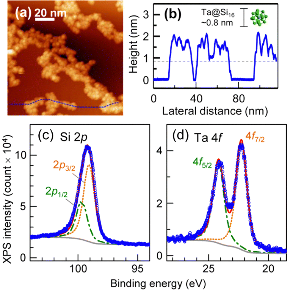 | ||
| Fig. 2 Characterization of Ta@Si16 deposited on a HOPG surface. (a) An STM image with (b) the height profile taken along a blue-dotted line in (a). XPS spectra for around (c) Si 2p and (d) Ta 4f core levels with the fitted results. Reproduced with permission from ref. 105. Copyright 2015 American Chemical Society. | ||
Given that Ta@Si16 is an alkali metal-like SA stable in a cationic state, it can readily release an electron to a neighboring electron accepting molecule. When deposited on C60 film, Ta@Si16 BCSAs are immobilized through the formation of CT complex Ta@Si16+–C60−. Each Ta@Si16 can be observed as single dots in the STM image of Ta@Si16 deposited on C60, indicating that stable immobilization was achieved.28 Systematic analyses of the height profile along with lateral sizes of Ta@Si16 on C60 revealed that Ta@Si16–C60 heterodimers tend to be vertical with thermal annealing.107 Electron transfer from Ta@Si16 to C60 was elucidated by the XPS analysis of the C 1s region shifting to a lower binding energy after the deposition of Ta@Si16 indicating that C60 is negatively charged.108
The chemical stability of Ta@Si16+ on a C60 surface was evaluated by XPS spectra with the gradual exposure of O2 gas. At the early stage of exposure, the Si 2p peak slightly shifted toward a higher binding energy and the Ta 4f peak is hardly changed. This finding indicated that Si is first oxidized and Ta is protected by the surrounding Si16 cage. With the increasing exposure amount, both Si and Ta are oxidized, indicating the cage has collapsed and a Ta atom is oxidized. Clear evidence for the cage collapse can be identified when nitric oxide (NO) is used as the oxidative gas. Given that NO adsorb molecularly to oxidized Ta that can be judged from the N 1s XPS spectrum appearing at 405.4 eV. The low exposure amount of NO gas results in the oxidation of Si atoms, and the XPS spectra of Ta 4f remains identical to that of the as-deposited Ta@Si16. With the increasing exposure amount, the Ta 4f peak shows an oxidized component which coincides with the appearance of the peak originating from molecularly adsorbed NO in the N 1s spectra as shown in Fig. 3, indicating that NO gas can behave as a collapse indicator of Si16 cage SAs.109
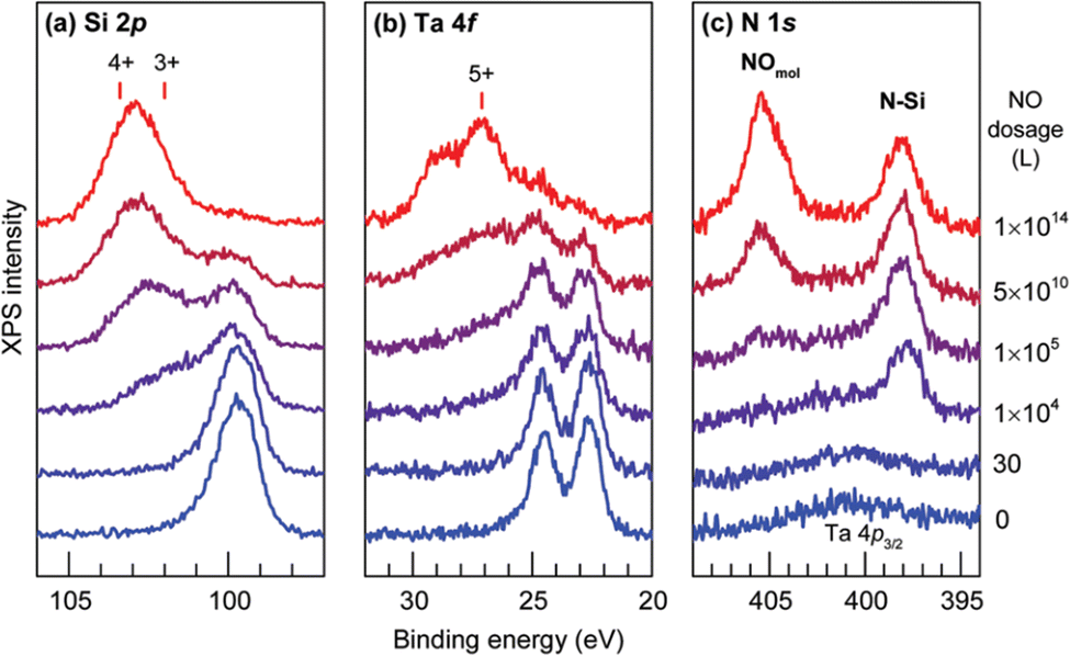 | ||
| Fig. 3 (a) Si 2p, (b) Ta 4f, and (c) N 1s core level XPS spectra for Ta@Si16 deposited on a C60 substrate before and after step by step exposure to NO. Reproduced from ref. 109 with permission from the Royal Society of Chemistry. | ||
The periodic dependence of the chemical reactivity of group-5 metal-atom (MV = V, Nb, and Ta) encapsulating M@Si16 BCSAs deposited on C60 was evaluated by the same method using O2 as the probing gas. Given that the total valence electron in MV@Si16 is the same, the alkali metal-like MV@Si16 becoming cationic on C60 was confirmed by the XPS spectra of the as-deposited specimen. However, the chemical reactivity toward O2 depends on the periodic number of MV; Nb@Si16 is the most reactive and Ta@Si16 is the most inert. The Si 2p peak with a higher binding energy originating from the oxidization of Si atoms most readily appears for Nb, then V, and finally Ta. The observed periodicity can be interpreted by the degree of electron density spreading outside the MV@Si16 obtained by the DFT calculation.106 The size-dependent reactivities of TaSin on C60 exhibit relatively high reactivity in small size n and a local minimum at Ta@Si16 along with Ta@Si17, which can be explained by the Si adatom structure of Ta@Si16.110
The CT complex formed between Ta@Si16 and the C60 molecular layer can be explained by considering the energetics for CT complexation.30 Endothermic dissociation limits (ΔE) of Ta@Si16+C60− and Ta@Si16−C60+ against the neutrals of M@Si16 and C60 can be calculated by the ionization energy and electron affinity of Ta@Si16 and C60. The value of ΔE is smaller for Ta@Si16+C60− compared to Ta@Si16−C60+, which is consistent with the XPS results. Although ΔE is positive, stabilization by Coulomb interaction and polarization of the C60 surroundings seems to overcome the endothermic gap. When a different group M is encapsulated, optimizing a charge state is important for the stable immobilization of M@Si16. In the case of an electron-donating (p-type) molecule such as HB-HBC, ΔE becomes smaller for M@Si16−HB-HBC+ compared to M@Si16+HB-HBC−, resulting in the electron transfer being in the opposite direction to that of C60. In fact, the chemical reactivity of halogen-like Lu@Si16 against molecular oxygen is suppressed when it is deposited on HB-HBC to form Lu@Si16−HB-HBC+ with satisfying 68 electron closure.30
For characterization of the behavior of M@Si16 BCSAs on different kinds of substrate, Ta@Si16 was deposited on strontium titanate (STO) as a representative of oxide substrate with step-by-step deposition. XPS measurement revealed that a layered film was formed. At the interface of Ta@Si16/STO, the partial oxidization of Ta@Si16 cause by an oxide substrate is recognized originating from the oxygen atoms in the substrate. Increasing the film thickness also increases the intact Ta@Si16 species because their multilayers are formed. Moreover, step-by-step O2 exposure to a thick film of 11 mL Ta@Si16 deposited on C60 revealed that only the outermost layer is oxidized as the “sacrificial layer” and inner Ta@Si16 is retained as non-oxidized as summarized in Fig. 4.111 These results indicated that the outermost and interface M@Si16 are inevitably oxidized but the inside layers are protected by these two layers making M@Si16 suitable for assembled materials.
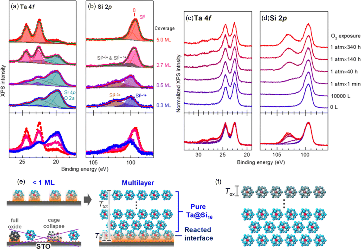 | ||
| Fig. 4 XPS spectra of Ta@Si16 deposited on a STO substrate at 0.3–5.0 mL ((a) Ta 4f and (b) Si 2p) and that of thick Ta@Si16 (11 mL) film before and after O2 exposure ((c) Ta 4f and (d) Si 2p). Schematic drawing of (e) interfacial oxidation of Ta@Si16 with <1 mL and multilayer and that of (f) surface oxidation penetrating a finite depth of Tox, which is not longer than the size of Ta@Si16. Reproduced with permission from ref. 111. Copyright 2020 American Chemical Society. | ||
4. M@Si16 and M@Ge16 as building blocks for superatom assembly
Considering the SA assembly by analogy with the atomic assembly, the geometry of spherical SAs is preferable due to their isotropic nature for assembling. Endohedrally doped cage BCSAs are a promising candidate for SA assembly due to their high symmetric structure and tunability with a dopant atom. As summarized in Section 2 and Fig. 1, M@Si16/M@Ge16 BCSAs are one of the most fascinating building blocks for SA assembly because of the controllability of their electronic states maintaining their highly symmetric structure. For assembled SAs, the energy levels of molecular orbitals are critical for charge transport. A p-type material with a hole as the charge carrier is preferable for molecules with a shallow HOMO level, and an electron transporting n-type material is preferable for molecules with a deep LUMO level.Organic semiconductors have been extensively studied as molecular conductors and for the control of electronic properties with a similar molecular structure. Fluorination or an additional functional group are well-established methodologies to control their electronic states; however, molecular packing at the heterojunction is generally unsuitable because the outer part of molecules is modified. M@Si16 and M@Ge16 BCSAs can now be regarded as an ideal class of materials that realize widely controllable electronic structures and the corresponding electronic states for carrier transport. The properties of M@Si16 as assembled systems were predicted theoretically. In early studies, Ti@Si16 and Zr@Si16 were suggested to intactly form a homodimer and their structures were explored.77 The hetero assembly of different M@Si16 was also predicted, and the findings implied that the p–n and p–i–n junction can be formed by group-3, -4, and -5 metal-atom encapsulated M@Si16. These results suggested the possibility of M@Si16 to be applied to optoelectronic devices.112 Moreover, the electronic properties of bulk state113,114 and 2D assembled film115 were investigated. However, an assembled state cannot be achieved until the large-scale synthesis of M@Si16 in the gas phase has been established.
The investigation of electrical conductor characteristics with a wide range of metal-atom encapsulation is an important task toward the application of M@Si16 and M@Ge16 assemblies for electronic devices. With innovation in the mass production of SAs in the gas phase and soft landing technique, the fabrication of SA-assembled films and their macroscopic characterization has been realized. In this section, our recent efforts of electrical characterization of M@Si16 and M@Ge16 BCSA films are described as SA assemblies.
4.1 Experimental method for M@Si16 and M@Ge16 assembled films
Experimental methods are briefly described, as previously reported elsewhere.33 With the use of the HiPIMS technique described in Section 2, M@Si16 cations or anions can be generated for more than 1 nA for various central metals as shown in the mass spectra of Fig. S1 (ESI†). Owing to the alkali metal-like nature of M@Si16 BCSA for group-5 metal-atom encapsulation, the cations of M@Si16+ are preferably generated for M = V, Nb, and Ta, satisfying the 68 electron shell closure. Similarly, the anions of M@Si16− are preferably generated for the group-3 metal-atom encapsulation of Lu@Si16 owing to the halogen-like nature. For group-4 metal-atom encapsulating M@Si16, a magic number behavior is found in their cations rather than in their anions.31 In the magnetron sputtering of M–Si mixed targets, the mass spectra for M@Si16± NCs with M = Ti, V, Nb and Ta evidently exhibit magic number behaviors, while with M = Lu, Zr and Hf, the mass spectra show less selective behaviors with slight enhancement of larger sizes such as M@Si17 and M@Si18.The difference in the magic number behaviors can be qualitatively understood by the geometrical factor of the radius of the M atom; the metallic bond radii of Lu (1.72 Å), Zr (1.59 Å) and Hf (1.56 Å) are larger than those of Ti (1.45 Å), V (1.31 Å), Nb (1.43 Å), and Ta (1.43 Å).116 When a larger metal-atom than internal cavity inside the Si16 cage is encapsulated, the Si16 cage is geometrically distorted.51 On the basis of the radius of the metal-atom, the metal-atom below 1.5 Å in the metallic radius can stabilize the geometry of M@Si16.
For a Ge16 cage, both Lu@Ge16− and Ta@Ge16+ are observed as the magic number behavior among M–Ge binary NCs, as shown in Fig. 5. The large cavity size of the Ge16 cage allows Lu to be stably encapsulated, and the Si16/Ge16 cage is geometrically more tolerant for small central atoms than for large central atoms. Ion currents of M@Si16± and M@Ge16± are typically more than 1 nA, which is sufficient to fabricate the assembled films with hundreds layer thickness in several to dozens of hours. The fabricated films are thick enough for the investigation of macroscopic characteristics, such as electrical conduction.
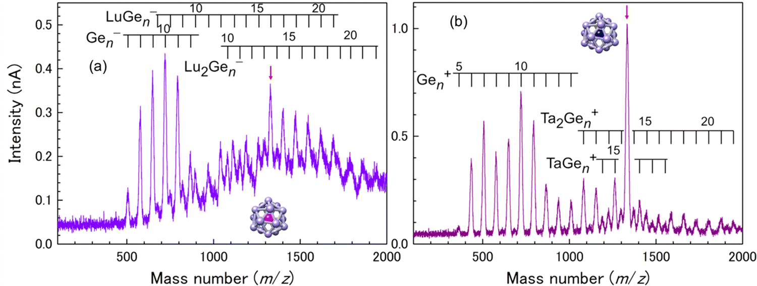 | ||
| Fig. 5 Mass spectra for M–Ge binary NC anions of (a) M = Lu and cations of (b) M = Ta. Red arrows indicate the peak corresponding to M@Ge16±. | ||
For the evaluation of electrical characteristics, the assembled films should be formed on an insulator layer between metallic electrodes, while avoiding charge-up of the deposited substrates with size-selected M@Si16± ions. An interdigitated Au electrode pattern was formed on the SiO2 surface, and Au electrodes were grounded to release the charge of incoming ions during deposition. The Au electrodes were connected to each other by Au wires and bridged to the Cu base plate by conductive silver paste as shown in Fig. 6(a).
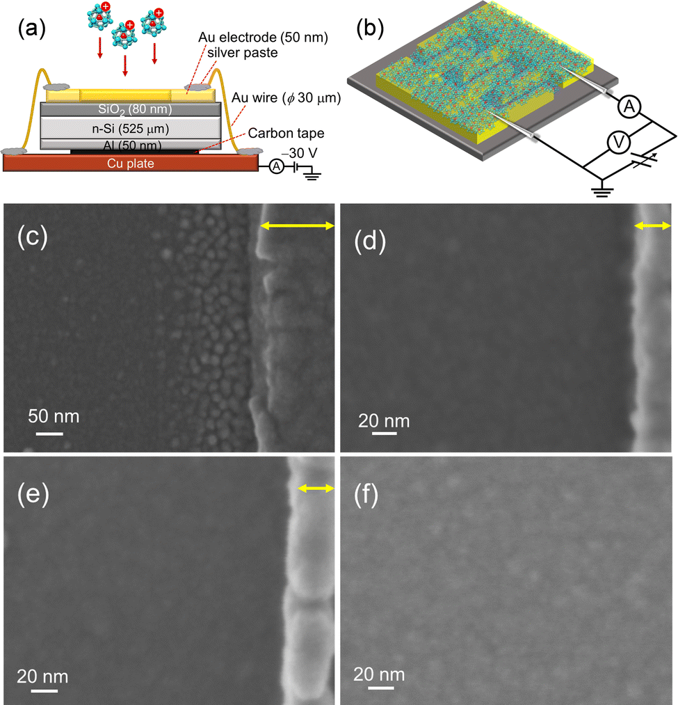 | ||
| Fig. 6 Schematics of (a) fabrication and (b) electrical conductivity measurement of M@Si16 assembled films. SEM images of Ta@Si16 assembled films near the Au electrode with a deposition amount of (c) 12 μC, (d) 18.5 μC, and (e) 46 μC. Au electrodes are shown on the right hand side of each figure indicated by yellow allows. (f) SEM image of the Ta@Si16 assembled film deposited on SiO2 between Au electrodes. Reproduced with permission from ref. 33. Copyright 2021 American Chemical Society. | ||
Toward the Au wire-connected substrate, the M@Si16± BCSA ions were deposited and neutralized by releasing the charge to the substrate through the Au wires. The typical deposition amount is 46 μC, which allows a fully spread film to form, that can fill the space between the electrodes. Fig. 6(c–e) show the scanning electron microscopy (SEM) images of Ta@Si16 film deposited on the substrate in the vicinity of Au electrodes with different deposition amounts of (c) 12, (d) 18.5, and (e) 46 μC. The SEM image in Fig. 6(c) showed that Ta@Si16 is predominantly deposited near the Au electrodes and formed island structures. A possible reason is that Ta@Si16+ ions preferentially release the charge to be neutral at an Au electrode. The clear island structures are imaged in contrast to the underlying substrate. With the increasing deposition amounts, the island structures seen at 12 μC deposition disappeared as shown in Fig. 6(d) and (e). A continuous film morphology covers all over the SiO2 layer between the Au electrodes. The SEM image between electrodes showed a continuous film at 46 μC deposition (Fig. 6(f)). When the continuous film is formed, electrical characteristics can be discussed from the viewpoint of M@Si16 assembled films. Moreover, fabricated films are composed of intact M@Si16 as evaluated by XPS spectra, showing that both Si 2p and Ta 4f can be reproduced by single-chemical components without any oxidation and any unexpected peak broadening.33 The following described the central metal dependence of M@Si16 and M@Ge16 films.
4.2 Electrical conduction of M@Si16 assembled films
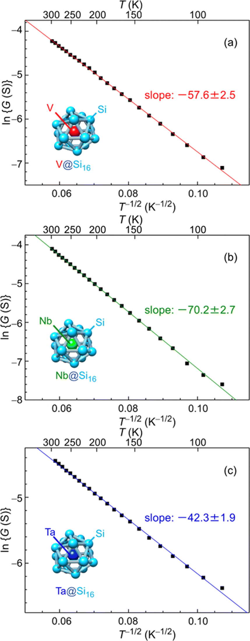
The electrical characteristics of group-5 metal-atom (MV = V, Nb and Ta) encapsulating Si cage BCSA (MV@Si16) assembled films33 will be discussed. Temperature (T = 87–300 K) dependent electrical conductance (G) was evaluated by current–voltage (I–V) measurements under vacuum (10−2 Pa) with voltage sweep at one terminal from 0 to 100 mV, and G was found to increase with T. Although semiconductor-like temperature dependence, plots based on band conduction showed that ln G is not proportional to T−1, indicating that MV@Si16 films hardly form a band structure. The electronic structures of isolated MV@Si16 showed that the singly occupied molecular orbital (SOMO) is a superatomic 1H orbital with multiple nodes, making the electronic overlap of neighboring MV@Si16 small.As an alternative conduction mechanism, variable range hopping (VRH) with strong electron correlation of the Efros–Shklovskii VRH (ES-VRH) model117 was investigated and the linear relationships of lnG vs. T−1/2 were obtained for all MV@Si16 as shown in Fig. 7. The validity of lnG ∝ T−1/2 was also confirmed by a Zabrodskii plot, where the exponent of T can be determined118 and the obtained value was close to about −0.5 for all MV@Si16. Although the conduction mechanism was the same for all MV encapsulation, the values of the slope of lnG vs. T−1/2 plots were dependent on MV. The value of the slope corresponds to the degree of how the localized electronic states are extended, which is called the localization length. The values were calculated to be 1.2 nm for V@Si16, 0.8 nm for Nb@Si16, and 2.2 nm for Ta@Si16, all of which were several times larger than the radius of M@Si16. This finding indicated that electronic states are not localized to single MV@Si16 but delocalized to the domain composed of several MV@Si16. The results might be due to the difference in degree of interaction between neighboring MV@Si16, revealing the period dependent collective properties in the BCSA-assembled films.
 | ||
| Fig. 7 Temperature dependent electrical conductance of MV@Si16 (MV = (a) V, (b) Nb, and (c) Ta) assembled films based on ES-VRH. Logarithm of conductance (lnG) versus T−1/2 for MV@Si16 films is plotted at 87–300 K, and the slope values are shown in each. Reproduced with permission from ref. 33. Copyright 2021 American Chemical Society. | ||
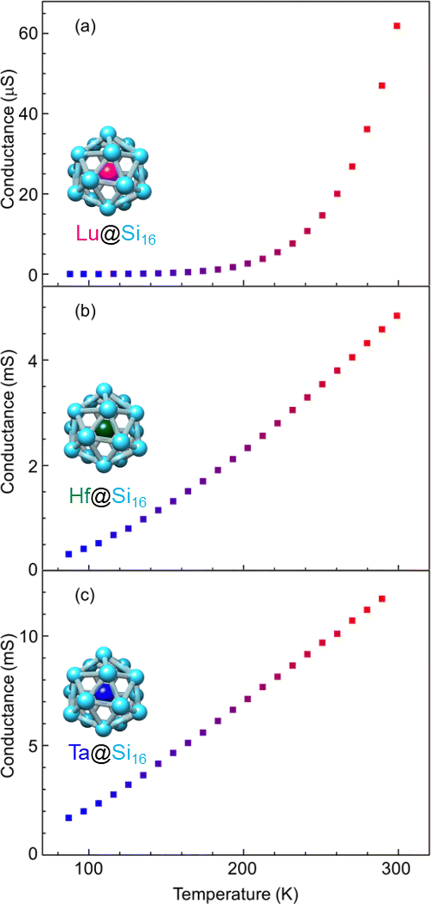
Group-3 and -4 metal-atom encapsulating SAs of Lu@Si16 and Hf@Si16 assembled systems were fabricated and characterized to further investigate the periodicity of M@Si16 BCSA-assembled systems. Fig. 8 shows the temperature-dependent electrical conductance of Lu@Si16, Hf@Si16, and Ta@Si16. The electrical conductance of the Lu@Si16 assembled film was 102–103 orders of magnitude smaller than those of Hf@Si16 and Ta@Si16 assembled films. Moreover, the temperature dependence of Lu@Si16 was more drastic, compared with those of qualitatively similar behaviors for Hf@Si16 and Ta@Si16. Given that isolated Lu@Si16 is one electron deficient to 68 e− shell closure, the carriers in the Lu@Si16 assembled system can be regarded as a hole.
 | ||
| Fig. 8 Metal-atom dependence of temperature-dependent electrical conductance for different group-3, -4, and -5; (a) Lu@Si16, (b) Hf@Si16, and (c) Ta@Si16 assembled films. | ||
The observed difference between group-3 encapsulating and group-4 and -5 encapsulating M@Si16 can be attributed to the carrier type difference in M@Si16. In fact, for a Si single crystal hole mobility is smaller than electron mobility,119 although the disordered structure might affect the mobility in M@Si16 assembled films. Neither band conduction nor hopping conduction can explain the observed temperature dependent conductance of Lu@Si16. Thus, further investigation is needed to reveal the electronic states and conduction mechanism of Lu@Si16. Direct confirmation of hole conduction is also required by applying the magnetic field based on Hall effect measurements for instance.
The electrical conduction behavior for Hf@Si16 assembled films can be denoted by ES-VRH with lnG proportional to T−1/2 as shown in Fig. 9(a). Given that isolated Hf@Si16 BCSA has a closed electronic shell with a HOMO–LUMO gap of 1.37 eV,51 the conduction mechanism of the Hf@Si16 assembled system should not be band conduction. Indeed, the conduction was characterized by ES-VRH originating from localized electronic states. Interestingly, the conduction mechanism was the same between rare-gas-like Hf@Si16 and alkali-like Ta@Si16, and the carrier of the Hf@Si16 assembled film can be inferred to be electrons. It seems reasonable that thermally excited electrons in the LUMO would be transported through the film with hopping conduction. The other group-4 metal-atom encapsulating M@Si16 of Ti@Si16 and Zr@Si16 assembled films similarly showed a lnG ∝ T−1/2 relationship, indicating that the conduction mechanism of all group-4 metal-atom encapsulating M@Si16 assembled films is ES-VRH (see the ESI,† Fig. S2).
 | ||
| Fig. 9 Temperature dependent electrical conductance of a Hf@Si16 assembled film based on the ES-VRH model; (a) as deposition and (b) after annealing at 423 K for 90 min in a vacuum. The logarithm of conductance (lnG) versus T−1/2 for Hf@Si16 films is plotted at 87–300 K, and the slope values are shown in each. | ||
One possible reason for the hopping conduction might be due to amorphous films and the fabrication of well-ordered crystalline M@Si16 leading to improved control over a collective behavior based on the isolated electronic structure of M@Si16. Post annealing of the Hf@Si16 assembled film was conducted at 415 K under vacuum (ca. 10−2 Pa) for 90 min to increase the crystallinity of the M@Si16 BCSA-assembled film. When brought back to room temperature, however, the conductance was dropped probably due to the oxidization of Hf@Si16 against residual gases during annealing as shown in Fig. 9(b). Although the temperature-dependent conductance of the annealed Hf@Si16 film showed lnG ∝ T−1/2 dependence with almost the same slope as before annealing, the absolute value of electrical conductance was reduced. Given that the conduction mechanism and localization length is identical before and after annealing, the result showed that crystallinity cannot be improved by the post annealing around 415 K along with the outermost layer oxidation of Hf@Si16, similar to the case of Ta@Si16 thick layers.111 An alternative strategy to improve the crystallinity is to increase the temperature while M@Si16 is deposited.
In addition to the bulk properties described above, electrical transport at the interface is an important target to elucidate because nanomaterials in contact with metals sometimes form Schottky barriers in unconventional ways.120 Interfacial properties such as Schottky barrier height can be characterized by scanning probe microscopy,121,122 which would be interesting to apply to M@Si16/M@Ge16 systems. In fact, the insertion of WSin NCs at metal/semiconductor interfaces can reduce the electron Schottky barrier height owing to the Fermi-level depinning,123 indicating the diverse potential applications of M@Si16/M@Ge16 SAs.
4.3 Electrical conduction of M@Ge16 assembled films
The M@Ge16 (M = Lu and Ta) BCSA-assembled films were fabricated to investigate the diversity of the building block instead of the outer Si16 cage as shown in Fig. 10. Ta@Ge16 films with the same deposition amount of 46 μC showed an electrical conductance of more than 100 mS at room temperature, which is one order of magnitude larger than that of the Ta@Si16 film. Low deposition amount of 33 μC corresponding to 72% of full deposition was also fabricated because contact resistance (typically several Ω) cannot be neglected in such high conduction. Given that the electrical conductance was still high, the properties were analyzed at a temperature below 210 K where the effect of contact resistance can be negligible. Temperature dependence can be reproduced by the ES-VRH model, which is identical to Ta@Si16 as shown in the ESI† (Fig. S3). The higher conductivity of Ta@Ge16 compared with that of Ta@Si16 implied that the metallic characters are enhanced, similar to the difference in nature between Si and Ge in bulk. The diversity of the M@Si16 family can be extended by not only substituting a central metal-atom, but also substituting cage atoms between Si and Ge, although the evaluation by a four terminal method would be a future task for the accurate characterization of Ta@Ge16 excluding the contact resistance. | ||
| Fig. 10 Temperature dependent conductance of (a) Lu@Ge16 and (b) Ta@Ge16 assembled films. | ||
For group-3 metal-atom encapsulation, the Ge16 cage has a larger internal cavity than the Si16 cage. Hence a large sized Lu atom can be stably encapsulated. As shown in Fig. 5(a),40,51 the magic number behavior of Lu@Ge16− was predominantly observed, which is in contrast to the smooth mass distributions for Lu@Si16− in Fig. S1 (ESI†). Fig. 10(a) shows the temperature dependence of electrical conductance of the Lu@Ge16 assembled film at 34 μC deposition. The electrical conductance significantly increased with the temperature, although the electrical conductance below 130 K was not shown due to a low signal-to-noise ratio. The temperature dependence for the Lu@Ge16 assembled film is qualitatively similar to that of the Lu@Si16 assembled film, implying that both are characterized by the hole conduction.
5. Summary and future prospects
In summary, we described the progress of NC research starting from the methodology of generating atomically precise NCs to surface immobilization and finally assembled film formation. The development of custom-made set-ups has always been required for the experimental investigation of novel physical and chemical properties of NCs in various levels of hierarchy. Early research in the gas phase showed that the size evolution of NC stability, reactivity, and structure can be understood in terms of the electronic shell model and unique geometric structures in combination with theoretical calculations. Exploratory research of magic number NCs revealed unexpected novel nanomaterials, such as metal-atom encapsulating Si cage NCs (M@Si16) that can be regarded as SAs. The high intensity NC beam generation system could be coupled with soft landing deposition, enabling exploration of the functionality of atomically precise NCs not only as a free-standing form but also as nanomaterials with a surface or NC assembled phase.The assembled film fabrication by M@Si16 BCSAs could be achieved with the high intensity NC source based on HiPIMS and a soft landing technique.33 High symmetric and electronic factor cooperatively stabilize M@Si16 BCSAs, enabling their assembly without deforming a unique caged structure to characterize macroscopic characteristics such as electrical conduction. The central metal dependence of M@Si16 was investigated along with germanium-cage SAs of M@Ge16 assembled films in an amorphous state to shed some light on superatomic periodicity in assembled materials.
The remaining challenges are as follows: (i) preparation of naked SAs in crystals, (ii) hetero connection of different SAs in the bulk phase, and (iii) fabrication of devices based on SAs as an active layer. The (i) challenge is important to understand how the isolated electronic states are delocalized to the band structure in a condensed phase. Experimental methods, such as angle resolved X-ray photoelectron spectroscopy, would be applicable to observe the band dispersion and stimulate the collaborative research in the field of condensed matter physics and material sciences. The (ii) challenge would lead to the corporative effect, which cannot be observed in a single component. Various characteristics can be achieved by heterojunction as shown in the Si-based and organic semiconductors. Microscopic characterization of the film morphology and electronic state at the heterojunction and film/electrode interface would also be important to gain deep insight into the origin of emergent functionality.
In an organic semiconductor, the ensemble of electron acceptors and electron donors is important for the emergence of functionality. The sub-monolayer deposition of M@Si16 on C60 formed the stable CT complex of M@Si16+–C60− when the central metal was group-5. The hetero layer formation of M@Si16 with p-type and n-type characteristics in the bulk phase would advance the realization of device fabrication in terms of challenge (iii). Taking photovoltaics as an example of potential device application, fine control of the HOMO and LUMO energy levels of the donor and acceptor materials allows efficient photoinduced electron transfer from the donors to the acceptors. Appropriate energy levels controlled by the central metal and cage element of M@Si16/M@Ge16 would lead to the improved device performance. Another merit for M@Si16 and M@Ge16 BCSA is their almost similar lattice constant. Hence, layers with different central metal would grow epitaxially. Given the experimental achievement for the electrical characteristics of M@Si16 and M@Ge16 assembled films with various M, this perspective would stimulate further experimental and theoretical studies toward the realization of designer functional SA-assembled materials.
Conflicts of interest
A. N. is an inventor on JAPAN patent JP 5493139, submitted by the JST agency and Ayabo Corp., which covers a nanocluster generator. The remaining authors declare no competing interests.Acknowledgements
Authors are grateful to Mr T. Chiba (Keio Univ.) for his support of electrical characterization of M@Si16 assembled films along with theoretical calculations, to Mr K. Nakamura (Keio Univ.) for his support of electrical characterization of M@Ge16 assembled films, and to Ms K. Tanaka (Center Service Facilities for Science and Technology Research, Keio Univ.) for SEM measurements. This work is partly supported by JSPS KAKENHI of Grants-in-Aid for Scientific Research (A) No. 19H00890, Challenging Research (Pioneering) No. 17H06226, Transformative Research Areas (A) “Hyper-Ordered Structures Science” (21H05573), and of Research Fellowships for Young Scientists Grant Number 19J22141.References
- U. Landman and W. D. Luedtke, Faraday Discuss., 2004, 125, 1–22 RSC.
- M. A. El-Sayed, Acc. Chem. Res., 2004, 37, 326–333 CrossRef CAS PubMed.
- U. Heiz, A. Sanchez, S. Abbet and W. D. Schneider, J. Am. Chem. Soc., 1999, 121, 3214–3217 CrossRef CAS.
- P. Ball, New Sci., 2005, 186, 30–33 Search PubMed.
- S. N. Khanna and P. Jena, Phys. Rev. Lett., 1992, 69, 1664–1667 CrossRef CAS PubMed.
- S. N. Khanna and P. Jena, Phys. Rev. B: Condens. Matter Mater. Phys., 1995, 51, 13705–13716 CrossRef CAS PubMed.
- A. Nakajima, T. Kishi, T. Sugioka and K. Kaya, Chem. Phys. Lett., 1991, 187, 239–244 CrossRef.
- E. R. Bernstein, Atomic and Molecular Clusters (Studies in Physical and Theoretical Chemistry), Elsevier, New York, 1990 Search PubMed.
- U. Heiz, F. Vanolli, L. Trento and W.-D. Schneider, Rev. Sci. Instrum., 1997, 68, 1986–1994 CrossRef CAS.
- K. Bromann, C. Félix, H. Brune, W. Harbich, R. Monot, J. Buttet and K. Kern, Science, 1996, 274, 956–958 CrossRef CAS PubMed.
- J. E. Barborini, G. Corbelli, G. Bertolini, P. Repetto, M. Leccardi, S. Vinati and P. Milani, New J. Phys., 2010, 12, 073001 CrossRef.
- J. Schmelzer Jr., S. A. Brown, A. Wurl, M. Hyslop and R. J. Blaikie, Phys. Rev. Lett., 2002, 88, 226802 CrossRef CAS PubMed.
- M. Mirigliano, F. Borghi, A. Podestà, A. Antidormi, L. Colombo and P. Milani, Nanoscale Adv., 2019, 1, 3119–3130 RSC.
- M. D. Pike, S. K. Bose, J. B. Mallinson, S. K. Acharya, S. Shirai, E. Galli, S. J. Weddell, P. J. Bones, M. D. Arnold and S. A. Brown, Nano Lett., 2020, 20, 3935–3942 CrossRef CAS PubMed.
- R. E. Palmer, R. Cai and J. Vernieres, Acc. Chem. Res., 2018, 51, 2296–2304 CrossRef CAS PubMed.
- M. Benelmekki, M. Bohra, J.-H. Kim, R. E. Diaz, J. Vernieres, P. Grammatikopoulos and M. Sowwan, Nanoscale, 2014, 6, 3532–3535 RSC.
- S. Mandal, A. C. Reber, M. Qian, P. S. Weiss, S. N. Khanna and A. Sen, Acc. Chem. Res., 2013, 46, 2385–2395 CrossRef CAS PubMed.
- A. Tao, P. Sinsermsuksakul and P. Yang, Nat. Nanotechnol., 2007, 2, 435–440 CrossRef CAS PubMed.
- H. Tsunoyama, C. Zhang, H. Akatsuka, H. Sekiya, T. Nagase and A. Nakajima, Chem. Lett., 2013, 42, 857–859 CrossRef CAS.
- S. Duffe, N. Grönhagen, L. Patryarcha, B. Sieben, C. Yin, B. von Issendorff, M. Moseler and H. Hövel, Nat. Nanotechnol., 2010, 5, 335–339 CrossRef CAS PubMed.
- M. Nakaya, T. Iwasa, H. Tsunoyama, T. Eguchi and A. Nakajima, Adv. Funct. Mater., 2014, 24, 1202–1210 CrossRef CAS.
- H. Tsunoyama, Y. Yamano, C. Zhang, M. Komori, T. Eguchi and A. Nakajima, Top. Catal., 2018, 61, 126–135 CrossRef CAS.
- H. Tsunoyama, H. Ito, M. Komori, R. Kobayashi, M. Shibuta, T. Eguchi and A. Nakajima, Catal. Sci. Technol., 2018, 8, 5827–5834 RSC.
- H. Tsunoyama, A. Ohnuma, K. Takahashi, A. Velloth, M. Ehara, N. Ichikuni, M. Tabuchi and A. Nakajima, Chem. Commun., 2019, 55, 12603–12606 RSC.
- A. Ohnuma, K. Takahashi, H. Tsunoyama, T. Inoue, P. Zhao, A. Velloth, M. Ehara, N. Ichikuni, M. Tabuchi and A. Nakajima, Catal. Sci. Technol., 2022, 12, 1400–1407 RSC.
- K. Yamagiwa, M. Shibuta and A. Nakajima, ACS Nano, 2020, 14, 2044–2052 CrossRef CAS PubMed.
- M. Shibuta, K. Yamamoto, T. Ohta, T. Inoue, K. Mizoguchi, M. Nakaya, T. Eguchi and A. Nakajima, ACS Nano, 2021, 15, 1199–1209 CrossRef CAS PubMed.
- M. Nakaya, T. Iwasa, H. Tsunoyama, T. Eguchi and A. Nakajima, Nanoscale, 2014, 6, 14702–14707 RSC.
- M. Shibuta, T. Inoue, T. Kamoshida, T. Eguchi and A. Nakajima, Nat. Commun., 2022, 13, 1336 CrossRef CAS PubMed.
- T. Kamoshida, M. Shibuta, T. Ohta, T. Eguchi and A. Nakajima, J. Phys. Chem. C, 2022, 126, 10889–10899 CrossRef CAS.
- H. Tsunoyama, H. Akatsuka, M. Shibuta, T. Iwasa, Y. Mizuhata, N. Tokitoh and A. Nakajima, J. Phys. Chem. C, 2017, 121, 20507–20516 CrossRef CAS.
- N. Hirata, Y. Katsura, H. Gunji, M. Tona, K. Tsukamoto, M. Eguchi, T. Ando and A. Nakajima, RSC Adv., 2021, 11, 39216–39222 RSC.
- T. Yokoyama, T. Chiba, N. Hirata, M. Shibuta and A. Nakajima, J. Phys. Chem. C, 2021, 125, 18420–18428 CrossRef CAS.
- P. Jena and Q. Sun, Superatoms: Principles, Synthesis and Applications, John Wiley & Sons Ltd, Hoboken, 2021 Search PubMed.
- C. M. Aikens, R. Jin, X. Roy and T. Tsukuda, J. Chem. Phys., 2022, 156, 170401 CrossRef CAS PubMed.
- H. Tsunoyama, M. Shibuta, M. Nakaya, T. Eguchi and A. Nakajima, Acc. Chem. Res., 2018, 51, 1735–1745 CrossRef CAS PubMed.
- J. Zhao, Q. Du, S. Zhou and V. Kumar, Chem. Rev., 2020, 120, 9021–9163 CrossRef CAS PubMed.
- K. Koyasu, J. Atobe, S. Furuse and A. Nakajima, J. Chem. Phys., 2008, 129, 214301 CrossRef PubMed.
- S. Furuse, K. Koyasu, J. Atobe and A. Nakajima, J. Chem. Phys., 2008, 129, 064311 CrossRef PubMed.
- J. Atobe, K. Koyasu, S. Furuse and A. Nakajima, Phys. Chem. Chem. Phys., 2012, 14, 9403–9410 RSC.
- U. Farooq, S. Naz, H.-G. Xu, B. Yang, X.-L. Xu and W.-J. Zheng, Coord. Chem. Rev., 2020, 403, 213095 CrossRef CAS.
- O. Echt, K. Sattler and E. Recknagel, Phys. Rev. Lett., 1981, 47, 1121–1124 CrossRef CAS.
- A. Herrmann, E. Schumacher and L. Wöste, J. Chem. Phys., 1978, 68, 2327–2336 CrossRef CAS.
- A. Herrmann, S. Leutwyler, E. Schumacher and L. Wöste, Helv. Chim. Acta, 1978, 61, 453–487 CrossRef CAS.
- K. Rademann, B. Kaiser, U. Even and F. Hensel, Phys. Rev. Lett., 1987, 59, 2319–2321 CrossRef CAS PubMed.
- K. Sattler, J. Mühlbach and E. Recknagel, Phys. Rev. Lett., 1980, 45, 821–824 CrossRef CAS.
- T. G. Dietz, M. A. Duncan, D. E. Powers and R. E. Smalley, J. Chem. Phys., 1981, 74, 6511–6512 CrossRef CAS.
- V. E. Bondybey and J. H. English, J. Chem. Phys., 1981, 74, 6978–6979 CrossRef CAS.
- S. Nonose, Y. Sone, K. Onodera, S. Sudo and K. Kaya, Chem. Phys. Lett., 1989, 164, 427–432 CrossRef CAS.
- W. Bouwen, P. Thoen, F. Vanhoutte, S. Bouckaert, F. Despa, H. Weidele, R. E. Silverans and P. Lievens, Rev. Sci. Instrum., 2000, 71, 54–58 CrossRef CAS.
- K. Koyasu, J. Atobe, M. Akutsu, M. Mitsui and A. Nakajima, J. Phys. Chem. A, 2007, 111, 42–49 CrossRef CAS PubMed.
- H. Haberland, M. Karrais, M. Mall and Y. Thurner, J. Vac. Sci. Technol. A Vacuum, Surfaces, Film., 1992, 10, 3266–3271 CrossRef CAS.
- R. Keller, F. Nöhmayer, P. Spädtke and M.-H. Schönenberg, Vacuum, 1984, 34, 31–35 CrossRef CAS.
- I. Katakuse, T. Ichihara, Y. Fujita, T. Matsuo, T. Sakurai and H. Matsuda, Int. J. Mass Spectrom. Ion Process., 1985, 67, 229–236 CrossRef CAS.
- S. Pratontep, S. J. Carroll, C. Xirouchaki, M. Streun and R. E. Palmer, Rev. Sci. Instrum., 2005, 76, 045103 CrossRef.
- A. Majumdar, D. Köpp, M. Ganeva, D. Datta, S. Bhattacharyya and R. Hippler, Rev. Sci. Instrum., 2009, 80, 095103 CrossRef PubMed.
- M. Hála, J. Čapek, O. Zabeida, J. E. Klemberg-Sapieha and L. Martinu, Surf. Coatings Technol., 2012, 206, 4186–4193 CrossRef.
- J. T. Gudmundsson, N. Brenning, D. Lundin and U. Helmersson, J. Vac. Sci. Technol. A Vacuum, Surfaces, Film., 2012, 30, 030801 CrossRef.
- C. Zhang, H. Tsunoyama, H. Akatsuka, H. Sekiya, T. Nagase and A. Nakajima, J. Phys. Chem. A, 2013, 117, 10211–10217 CrossRef CAS PubMed.
- C. Zhang, H. Tsunoyama, Y. Feng and A. Nakajima, J. Phys. Chem. C, 2016, 120, 5667–5672 CrossRef CAS.
- P. Pyykkö, J. Organomet. Chem., 2006, 691, 4336–4340 CrossRef.
- X. Li, B. Kiran, J. Li, H. Zhai and L. Wang, Angew. Chem., Int. Ed., 2002, 41, 4786–4789 CrossRef CAS PubMed.
- D. M. P. Mingos, Acc. Chem. Res., 1984, 17, 311–319 CrossRef CAS.
- D. M. P. Mingos, T. Slee and L. Zhenyang, Chem. Rev., 1990, 90, 383–402 CrossRef CAS.
- J. E. McGrady, F. Weigend and S. Dehnen, Chem. Soc. Rev., 2022, 51, 628–649 RSC.
- W. A. de Heer, Rev. Mod. Phys., 1993, 65, 611–676 CrossRef CAS.
- W. D. Knight, K. Clemenger, W. A. de Heer, W. A. Saunders, M. Y. Chou and M. L. Cohen, Phys. Rev. Lett., 1984, 52, 2141–2143 CrossRef CAS.
- O. C. Thomas, W. Zheng, S. Xu and K. H. Bowen Jr., Phys. Rev. Lett., 2002, 89, 213403 CrossRef PubMed.
- R. E. Leuchtner, A. C. Harms and A. W. Castleman Jr., J. Chem. Phys., 1991, 94, 1093–1101 CrossRef CAS.
- A. Nakajima, K. Hoshino, T. Naganuma, Y. Sone and K. Kaya, J. Chem. Phys., 1991, 95, 7061–7066 CrossRef CAS.
- Z. Luo, C. J. Grover, A. C. Reber, S. N. Khanna and A. W. Castleman Jr., J. Am. Chem. Soc., 2013, 135, 4307–4313 CrossRef CAS PubMed.
- K. Minamikawa, S. Sarugaku, M. Arakawa and A. Terasaki, Phys. Chem. Chem. Phys., 2022, 24, 1447–1455 RSC.
- S. M. Beck, J. Chem. Phys., 1987, 87, 4233–4234 CrossRef CAS.
- S. M. Beck, J. Chem. Phys., 1989, 90, 6306–6312 CrossRef CAS.
- M. Sanekata, T. Koya, S. Nagao, Y. Negishi, A. Nakajima and K. Kaya, Trans. Mater. Res. Soc. Japan, 2000, 25, 1003–1006 CAS.
- M. Ohara, K. Miyajima, A. Pramann, A. Nakajima and K. Kaya, J. Phys. Chem. A, 2002, 106, 3702–3705 CrossRef CAS.
- V. Kumar and Y. Kawazoe, Phys. Rev. Lett., 2001, 87, 045503 CrossRef CAS PubMed.
- V. Kumar, T. M. Briere and Y. Kawazoe, Phys. Rev. B: Condens. Matter Mater. Phys., 2003, 68, 155412 CrossRef.
- J. Ulises Reveles and S. N. Khanna, Phys. Rev. B: Condens. Matter Mater. Phys., 2006, 74, 035435 CrossRef.
- P. Guo, Z.-Y. Ren, A.-P. Yang, J.-G. Han, J. Bian and G.-H. Wang, J. Phys. Chem. A, 2006, 110, 7453–7460 CrossRef CAS PubMed.
- S.-J. Lu, H.-G. Xu, X.-L. Xu and W.-J. Zheng, J. Phys. Chem. A, 2020, 124, 9818–9831 CrossRef CAS PubMed.
- K. Wang, H.-Y. Zhao, L. Miao, Z.-Z. Jia, G.-J. Yin, X.-D. Zhu, R. Moro, B. von Issendorff and L. Ma, J. Phys. Chem. A, 2022, 126, 1329–1335 CrossRef CAS PubMed.
- K. Koyasu, M. Akutsu, M. Mitsui and A. Nakajima, J. Am. Chem. Soc., 2005, 127, 4998–4999 CrossRef CAS PubMed.
- T. Inoue, T. Ichikawa, K. Matsunaga, R. Birumachi, K. Nakamura and A. Nakajima, J. Electrochem. Soc., 2022, 169, 102511 CrossRef.
- W. Harbich, S. Fedrigo, F. Meyer, D. M. Lindsay, J. Lignieres, J. C. Rivoal and D. Kreisle, J. Chem. Phys., 1990, 93, 8535–8543 CrossRef CAS.
- S. Fedrigo, W. Harbich and J. Buttet, Phys. Rev. B: Condens. Matter Mater. Phys., 1993, 47, 10706–10715 CrossRef CAS PubMed.
- E. C. Honea, A. Ogura, C. A. Murray, K. Raghavachari, W. O. Sprenger, M. F. Jarrold and W. L. Brown, Nature, 1993, 366, 42–44 CrossRef CAS.
- K. Judai, K. Sera, S. Amatsutsumi, K. Yagi, T. Yasuike, S. Yabushita, A. Nakajima and K. Kaya, Chem. Phys. Lett., 2001, 334, 277–284 CrossRef CAS.
- M. Mitsui, S. Nagaoka, T. Matsumoto and A. Nakajima, J. Phys. Chem. B, 2006, 110, 2968–2971 CrossRef CAS PubMed.
- S. Nagaoka, T. Matsumoto, E. Okada, M. Mitsui and A. Nakajima, J. Phys. Chem. B, 2006, 110, 16008–16017 CrossRef CAS PubMed.
- H. Yasumatsu, T. Hayakawa, S. Koizumi and T. Kondow, J. Chem. Phys., 2005, 123, 124709 CrossRef PubMed.
- Y. Watanabe and N. Isomura, J. Vac. Sci. Technol. A: Vac. Surf. Films, 2009, 27, 1153–1158 CrossRef CAS.
- U. Heiz and E. L. Bullock, J. Mater. Chem., 2004, 14, 564–577 RSC.
- S. Vajda and M. G. White, ACS Catal., 2015, 5, 7152–7176 CrossRef CAS.
- M. Rondelli, G. Zwaschka, M. Krause, M. D. Rötzer, M. N. Hedhili, M. P. Högerl, V. D’Elia, F. F. Schweinberger, J.-M. Basset and U. Heiz, ACS Catal., 2017, 7, 4152–4162 CrossRef CAS.
- Y. Lei, F. Mehmood, S. Lee, J. Greeley, B. Lee, S. Seifert, R. E. Winans, J. W. Elam, R. J. Meyer, P. C. Redfern, D. Teschner, R. Schölgl, M. J. Pellin, L. A. Curtiss and S. Vajda, Science, 2010, 328, 224–228 CrossRef CAS PubMed.
- A. S. Crampton, M. D. Rötzer, U. Landman and U. Heiz, ACS Catal., 2017, 7, 6738–6744 CrossRef CAS.
- M. D. Rötzer, M. Krause, A. S. Crampton, U. Heiz, B. Yoon and U. Landman, ACS Catal., 2020, 10, 1799–1809 CrossRef.
- H. Yasumatsu and N. Fukui, J. Phys. Chem. C, 2015, 119, 11217–11223 CrossRef CAS.
- A. Beniya, K. Miwa, H. Hirata, Y. Watanabe and S. Higashi, ACS Catal., 2022, 12, 1977–1985 CrossRef CAS.
- K. W. Edmonds, C. Binns, S. H. Baker, M. J. Maher, S. C. Thornton, O. Tjernberg and N. B. Brookes, J. Magn. Magn. Mater., 2000, 220, 25–30 CrossRef CAS.
- J. E. Scheerder, T. Picot, N. Reckinger, T. Sneyder, V. S. Zharinov, J.-F. Colomer, E. Janssens and J. Van de Vondel, Nanoscale, 2017, 9, 10494–10501 RSC.
- J. E. Scheerder, S. Liu, V. S. Zharinov, N. Reckinger, J.-F. Colomer, H.-P. Cheng, J. Van de Vondel and E. Janssens, Adv. Mater. Interfaces, 2018, 5, 1801274 CrossRef.
- W. Keijers, R. Murugesan, G. Libeert, J. E. Scheerder, B. Raes, S. Brems, S. De Gendt, M. Houssa, E. Janssens and J. Van de Vondel, J. Phys Mater., 2021, 4, 045005 CrossRef CAS.
- M. Shibuta, T. Ohta, M. Nakaya, H. Tsunoyama, T. Eguchi and A. Nakajima, J. Am. Chem. Soc., 2015, 137, 14015–14018 CrossRef CAS PubMed.
- M. Shibuta, T. Kamoshida, T. Ohta, H. Tsunoyama and A. Nakajima, Commun. Chem., 2018, 1, 50 CrossRef.
- M. Nakaya, T. Iwasa, H. Tsunoyama, T. Eguchi and A. Nakajima, J. Phys. Chem. C, 2015, 119, 10962–10968 CrossRef CAS.
- T. Ohta, M. Shibuta, H. Tsunoyama, T. Eguchi and A. Nakajima, J. Phys. Chem. C, 2016, 120, 15265–15271 CrossRef CAS.
- M. Shibuta, T. Niikura, T. Kamoshida, H. Tsunoyama and A. Nakajima, Phys. Chem. Chem. Phys., 2018, 20, 26273–26279 RSC.
- M. Shibuta, M. Huber, T. Kamoshida, K. Terasaka, M. Hatanaka, G. Niedner-Schatteburg and A. Nakajima, J. Phys. Chem. C, 2022, 126, 4423–4432 CrossRef CAS.
- M. Shibuta, R. Takano and A. Nakajima, J. Phys. Chem. C, 2020, 124, 28108–28115 CrossRef CAS.
- T. Iwasa and A. Nakajima, J. Phys. Chem. C, 2012, 116, 14071–14077 CrossRef CAS.
- H. Cantera-López, L. C. Balbás and G. Borstel, Phys. Rev. B: Condens. Matter Mater. Phys., 2011, 83, 075434 CrossRef.
- M. B. Torres, E. M. Fernández and L. C. Balbás, J. Phys. Chem. C, 2011, 115, 335–350 CrossRef CAS.
- J. Liu, P. Guo, J. Zheng, P. Zhao, Z. Jiang and L. Shen, J. Phys. Chem. C, 2020, 124, 6861–6870 CrossRef CAS.
- Handbook of Chemistry and Physics, ed. D. R. Lide, CRC, Boston, 88th edn, 2007 Search PubMed.
- B. I. Shklovskii and A. L. Efros, Electronic Properties of Doped Semiconductors, Springer, Berlin, 1984 Search PubMed.
- A. G. Zabrodskii and K. N. Zinov’eva, Sov. Phys. JETP, 1984, 59, 425–433 Search PubMed.
- S. M. Sze and K. K. Ng, Physics of Semiconductor Devices, John Wiley & Sons, Inc., Hoboken, New Jersey, 3rd edn, 2006 Search PubMed.
- L. Amirav and M. Wächtler, Nano Lett., 2022, 22, 9783–9785 CrossRef CAS PubMed.
- G. D. J. Smit, S. Rogge and T. M. Klapwijk, Appl. Phys. Lett., 2002, 80, 2568–2570 CrossRef CAS.
- F. Ruffino, M. G. Grimaldi, F. Giannazzo, F. Roccaforte and V. Raineri, Appl. Phys. Lett., 2006, 89, 1–4 Search PubMed.
- N. Okada, N. Uchida and T. Kanayama, Appl. Phys. Lett., 2014, 104, 062105 CrossRef.
Footnote |
| † Electronic supplementary information (ESI) available. See DOI: https://doi.org/10.1039/d3cp00120b |
| This journal is © the Owner Societies 2023 |