
 Open Access Article
 This Open Access Article is licensed under a
 Creative Commons Attribution 3.0 Unported Licence
Enhanced charge transport across molecule–nanoparticle–molecule sandwiches†‡
P.
Zhou
 ab,
X.
Qiao
b,
D. C.
Milan
b,
S. J.
Higgins
b,
A.
Vezzoli
*b and
R. J.
Nichols
*b
ab,
X.
Qiao
b,
D. C.
Milan
b,
S. J.
Higgins
b,
A.
Vezzoli
*b and
R. J.
Nichols
*b
aYangzhou Polytechnic Institute, No. 199, Huayang West Road, Yangzhou City, Jiangsu Province, China
bDepartment of Chemistry, University of Liverpool, Crown St, Liverpool, L69 7ZD, UK. E-mail: nichols@liverpool.ac.uk; andrea.vezzoli@liverpool.ac.uk
First published on 20th February 2023
Abstract
The electrical properties of large area molecular devices consisting of gold nanoparticles (GNPs) sandwiched between a double layer of alkanedithiol linkers have been examined. These devices have been fabricated by a facile bottom-up assembly in which an alkanedithiol monolayer is first self-assembled on an underlying gold substrate followed by nanoparticle adsorption and then finally assembly of the top alkanedithiol layer. These devices are then sandwiched between the bottom gold substrates and a top eGaIn probe contact and current–voltage (I–V) curves recorded. Devices have been fabricated with 1,5-pentanedithiol, 1,6-hexanedithiol, 1,8-octanedithiol and 1,10-decanedithiol linkers. In all cases the electrical conductance of the double SAM junctions with GNPs is higher than the corresponding and much thinner single alkanedithiol SAM. Competing models for this enhanced conductance are discussed and it is suggested to have a topological origin arising from how the devices assemble or structure during the fabrication, which gives more efficient cross device electron transport pathways without the GNPs producing short circuits.
Introduction
Metal nanoparticles have featured strongly in molecular and nano-electronics and electrochemistry, where their ability to store and control the flow of charge has been exploited. Composite hybrid films of self-assembled monolayers and gold nanoparticles have been considered for many applications such as electronics devices, information storage, analysis, plasmonic devices and electronic skin.1,2 In molecular and nano-electronics nanoparticles of sufficiently small size can be assembled in devices where the flow of charge across a tunnelling junction is restricted due to strong electrostatic repulsions, inhibiting nanoparticle charging unless a sufficient bias is applied to the device. This then results in characteristic non-linear current–voltage behaviour referred to as Coulomb blockades and staircases, which can be controlled by the nanoparticle size, the junction electrical (RC) characteristics and the temperature.3,4 It has even been possible to study the electrical characteristics of ultra-small metal clusters within single molecular wires containing a discrete number of metal atoms defined by atomically-precise synthesis.5–7 Metal nanoparticles have also featured widely in electrochemistry, where both their catalytic and electron transfer characteristics have been exploited.8 Very interesting electron transfer characteristics have been observed for gold nanoparticles assembled on-top of insulating self-assembled monolayers (ML) built on conductive electrodes. The nanoparticles decorating the top of these otherwise insulating SAMs can be very good conduits for electron transfer to soluble (freely diffusing) redox systems in solution. Here, electron transfer to the solution redox species is blocked by the SAM, but the nanoparticle acts as a charge reservoir (similar to the electron sink9 concept used in cluster chemistry) that allows facile electrode → nanoparticle charge transfer, followed by a rate-determining ET step to the redox system. Further studies then showed that the ET enhancement takes place in the local surroundings of the metal nanoparticle,10 that redox systems covalently bonded to the nanoparticle participate in the same 2-step mechanism,11,12 and that there is a subtle interplay between the size of the nanoparticle and the length of the insulating molecule assembled in a monolayer that can result either in enhanced or hindered ET.13–16 Chazalviel and Allongue developed an elegant model to explain electron transfer at the electrode–SAM–NP–electrolyte interface being a result of the electrode potential drop almost completely manifesting itself at the NP–electrolyte interface up to a certain SAM thickness, thereby giving length-independent ET rates to the redox system to this SAM thickness.15Given the remarkable electrical and electrochemical characteristics of individual nanoparticles it is not surprising that there has also been interest in nanoparticles assembled into large area two- and three-dimensional films on electrodes. Applications have been found in optics, electrochemistry, substrates for surface enhanced Raman scattering (SERS)17 and sensing.18 Composite organic-nanoparticle film materials may in the future offer applications in molecular and organic electronics through integration into solid-state devices. A defined and convenient bottom-up fabrication approach is to sandwich metal nanoparticles between a double SAM layer, with one SAM layer below and one above the intermediary nanoparticle layer. This can also be extended to build up multilayers using efficient stepwise device growth methods.19 Seo et al. have fabricated double SAM devices with gold nanoparticles sitting in between layers of cobalt(II) bis-terpyridine SAMs.20 Such devices were found to be surprisingly conductive given their molecular length. The authors concluded that charge flow through these devices is by sequential tunnelling conduction through the highest occupied molecular orbitals (HOMOs) of the Co(II) bis-terpyridine SAMs, with the gold NPs in the middle of the double layer junction affecting the HOMO levels position and thereby promoting fast electron transfer. This is clearly a complex junction assembled with the combination of redox active molecular wires with accessible HOMO levels interconnected by gold nanoparticle linkers, but the enhanced transport properties do show the potential of such assemblies in molecular electronics. These collected results highlight the promise that such “sandwich” systems have for solid-state devices. Intrigued by these opportunities it was decided to investigate the electrical properties of double SAM – nanoparticle assemblies linked instead by electrically benign alkanedithiol SAMs. These archetypical molecular linkers have larger HOMO–LUMO gaps and are simple tunnelling bridges, thereby providing more straightforward electrical circuit elements for evaluating the influence of the sandwiched gold nanoparticles on the device electrical response. With this aim in mind, these structures were fabricated into metal–molecule–nanoparticle–molecule–oxide–metal large-area molecular junctions using a stepwise method (Fig. 1) and their charge transport behaviour probed with the eGaIn soft contact method.21
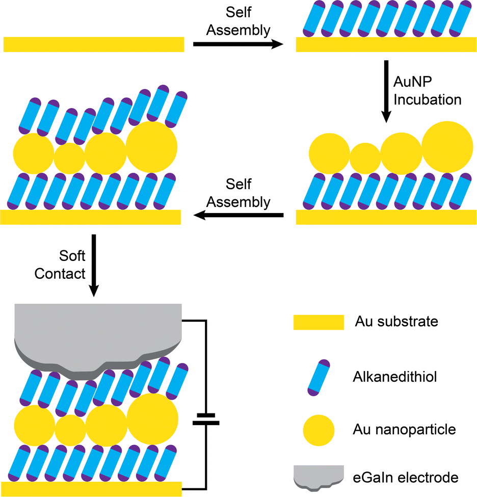 | ||
| Fig. 1 Stepwise growth method used in this contribution. | ||
Results and discussion
The devices were grown stepwise (Fig. 1), to form Au electrode – alkanedithiol – gold NP – alkanedithiol structures. The first structures studied involved 1,6-hexanedithiol, but the electrical properties of devices with 1,5-pentanedithiol, 1,8-octanedithiol and 1,10-decanedithiol double SAM layers using the same fabrication protocols are described later. After depositing a monolayer of 1,6-hexanedithiol on a gold-on-glass slide (16 h adsorption from 1 mM ethanolic solution), the slide was incubated overnight (∼12 h) in a solution of 8 ± 2 nm diameter uncapped Au nanoparticles freshly prepared in toluene,22 to ensure a high-coverage layer was assembled on the surface of the monolayer. After this, a further monolayer of 1,6-hexanedithiol was adsorbed on the nanoparticles (16 h adsorption from 1 mM ethanolic solution), to yield the sandwich structure. Cyclic voltammetry and AFM nanolithographic techniques23 were used to characterise each step of the device growth. After deposition of the first molecular layer, the electrochemical response towards the ferrocene/ferrocenium redox couple was completely blocked (Fig. 2a), in good agreement with the literature.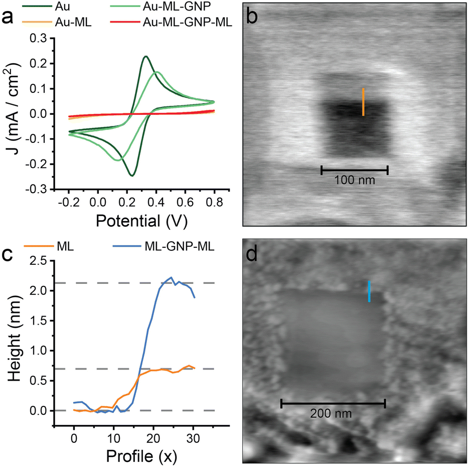 | ||
| Fig. 2 Characterisation of the stepwise device assembly. (a) Cyclic voltammetry on the various steps of device growth, from the bare Au slide (Au), to a 1,6-hexanedithiol monolayer (Au–ML), after adsorption of Au NPs (Au–ML–GNP) and after assembly of the second 1,6-hexanedithiol monolayer (Au–ML–GNP–ML). (b) AFM nanolithography on a single 1,6-hexanedithiol monolayer, where a 100 × 100 nm square was carved by applying a 20 nN force to the tip. (c) AFM profile after carving on a single 1,6-hexanedithiol monolayer (ML) and the final dithiol–nanoparticle–dithiol device (ML–GNP–ML). (d) AFM nanolithography on the final device, where a 200 × 200 nm square was carved by applying 20 nN to the cantilever. CV in (a) obtained in a 3-electrode cell, using a 1 cm2 Au-on-glass substrate as working electrode, a platinum wire reference electrode and a platinum mesh counter electrode, in acetonitrile with 0.1 M NBu4BF4 as supporting electrolyte and 1 mM ferrocene as analyte. AFM imaging performed at 0.3 nN force setpoint. Greyscale in (b) is 0–1.3 nm and in (d) is 0–17.1 nm. | ||
AFM carving experiments were then performed, where an adsorbate on a hard substrate is shaved away by scanning with a relatively high force applied to the cantilever. After carving a 100 × 100 nm square (Fig. 2b), measurement of the resulting profile gave a monolayer thickness of 0.73 nm (Fig. 2c), commensurate with a 1,6-hexanedithiol monolayer lying on the substrate at a tilt angle of 30–35°.24 After incubation in the nanoparticle solution the electrochemical response was reinstated only to be blocked again when a further layer of insulating alkanedithiol was assembled on top (Fig. 2a). The effective charge transfer seen in the electrochemistry of the Au–ML–GNP film in contrast to Au–ML and Au–ML–GNP–ML is a hallmark of nanoparticle-enhanced ET as discussed in the introduction. AFM experiments on the second and third stage of device growth were less conclusive, as the cantilever-tip assembly is known to disturb the nanoparticles position when the instrument is operated in contact mode (necessary for AFM nanolithography), but carving experiments showed an increased thickness of the deposited layer (Fig. 2c and d). Furthermore, adsorption of material (such as the Au NPs) on the cantilever could change its mechanical properties and the shape of the tip, resulting in unreliable Z calibration. Overall, the electrochemical data points towards a successful nanoparticle-mediated electron transfer in the Au–molecule–NP assembly, in excellent agreement with the published literature on the subject as highlighted in the introduction.
After growth of the monolayer assemblies on the Au substrate, they were contacted using the eGaIn (gallium–indium eutectic) liquid drop method.21 This technique has been developed as a safer and cleaner alternative to the Hg drop electrode method, as it uses non-toxic materials and has fewer contamination issues. The eGaIn method has been successfully used in the literature to characterise charge transport,25,26 light emission27 and thermoelectric phenomena28 in large-area molecular junctions. In brief, a microelectrode is fabricated by suspending a drop of eGaIn from a microsyringe needle on top of a sacrificial substrate, and then retracting the needle slowly using a micromanipulator. The drop of eGaIn pinches into a hourglass shape, that is subsequently ruptured to yield a sharp conical tip. The tip does not retract into a spherical shape as would happen with Hg due to the presence of a mouldable oxide layer on its surface. The eGaIn tip is then brought into contact with the monolayer or monolayer–nanoparticle–monolayer using a micromanipulator for coarse approach and a piezo stack for the final few μm. A bias voltage is applied between the tip and the Au substrate, and the current signal is acquired. Contact with the monolayer is monitored with a microscope (convergence of the conical tip and its reflection indicates contact) and confirmed by an increase of the current signal from its noise level (approximately 65 pA in our setup). As a contact is in place, a sawtooth waveform is applied to the tip-substrate bias and the current is continuously recorded within the bias window of interest (in this study, ±1.5 V). The diameter of each junction is also measured at the point of convergence of the eGaIn tip with its reflection and used to calculate the current density J = A cm2. About 50 J–V characteristics were recorded before lifting the tip, moving it to a different area of the substrate and repeating the process. After three uses of each tip, a new one was formed on a sacrificial substrate to reduce contamination and increase reproducibility of the data. Several hundred individual J–V characteristics were acquired for each sample and compiled into 2D maps of current density versus bias voltage. Automated algorithms were used to discard short-circuited traces (when the current preamplifier is saturated) and traces where the junction failed during the J–V recording (either short-circuited or ruptured at the molecule/Ga2O3 interface) but no further data selection was performed on the acquired datasets. Technical details on the eGaIn technique and the equipment used are available in the “Materials and Methods” section.
eGaIn measurements on the simple 1,6-hexanedithiol monolayer showed a J–V shape in good agreement with the literature on similar saturated compounds (Fig. 3a). The molecular junctions showed negligible rectification even in the presence of an asymmetric Au–molecule–Ga2O3/eGaIn structure, as expected in the absence of a strong dipole at the molecule/Ga2O3 interface.29,30 Repeating the same measurements on the monolayer–nanoparticle–monolayer assembly yielded unexpected results. Current density over the entire bias voltage window is greater than for the single monolayer (Fig. 3c), showing that Au–hexanedithiol–GNP–hexanedithiol double layer SAM interconnected with nanoparticles is more conductive than the single SAM of 1,6-hexanedithiol. It is noted here that we were unable to obtain any meaningful data when we attempted the fabrication of Au–ML–GNP–eGaIn junctions, most probably due to the formation of intermetallic Au–Ga alloys enabled by the absence of a ligand shell surrounding the Au nanoparticles.31
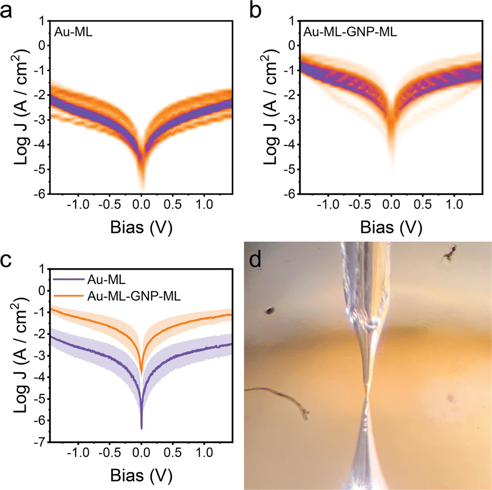 | ||
| Fig. 3 eGaIn measurements. (a) 2D map of current density vs. bias voltage compiled from 791 Au/1,6-hexanedithiol/Ga2O3/eGaIn junctions. (b) 2D map of current density vs. bias voltage compiled from 1616 Au/1,6-hexanedithiol/AuNPs/1,6-hexanedithiol/Ga2O3/eGaIn junctions. (c) Comparison between the average J–V characteristics calculated from the same data used in (a and b) by Gaussian fitting of each vertical slice of the 2D map (binsize = 20 mV). Shaded area is the error (standard deviation). (d) Photograph of a large-area junction (in this photograph, 36 μm2), fabricated with the eGaIn technique. The junction is located at the centre, where the tip and its reflection on the Au substrate meet. Maps in (a and b) compiled with 10 bins per decade and 50 bins per V. | ||
The unexpectedly enhanced conductance for the Au–ML–GNP–ML structure was analysed to establish whether it also occurs for different monolayer lengths. Electrical data is shown in Fig. 4 for such devices using 1,5-pentanedithiol and 1,10-decanedithiol (complementary electrical data for devices using 1,8-octanedithiol is available in the ESI‡ in Section S1 and Fig. S1), comparing the monolayer SAM device with the Au–ML–GNP–ML device. An identical fabrication protocol was used as that described for 1,6-hexanedithiol. In each case the double layer SAM with interconnecting GNPs shows higher conductance than for its equivalent monolayer SAM. Fitting the results to a simple tunnelling model where the current density J decays logarithmically with the length L of the molecular wire as J = Jc exp(−βL), allows us to extract the attenuation factor β for the two series of devices. While for the simple alkanedithiol series the attenuation per CH2 unit is βN = 1.05 (in good agreement with previous results),32,33 current is less attenuated with length in the sandwich devices, with βN = 0.61. This enhanced current and the reduced attenuation factor for the double layer structures might have several possible origins, which are considered in the following text. An interpretation based on a short-circuit of the junction through the nanoparticle was discounted, as this would result in either (i) metallic transport characteristics with much higher values of J if the entire junction is short-circuited (behaving therefore like a simple Au/Ga2O3/eGaIn microcontact) or (ii) charge transport behaviour identical to the single 1,6-hexanedithiol monolayer if only either the Au substrate–Au nanoparticle or the Au–Ga2O3 portion of the nanoscale assembly are affected. A second possibility is that the nanoparticles are efficiently mediating and enhancing charge transport. As discussed in the introduction, nanoparticles assembled onto blocking and insulating alkanethiol SAMs are effective conduits of electron transfer between SAM-covered surfaces and redox couples in the electrolyte solution. In the absence of nanoparticles the SAM blocks electron transfer, but with the nanoparticle the electrode potential drop occurs almost completely at the nanoparticle–electrolyte interface up to a certain SAM thickness, thereby facilitating effective and fast electron transfer to the redox system in solution (up to a certain SAM thickness).15 This model is however not relevant for the Au–ML–GNP–ML structures since the gold nanoparticles in these structures are passivated by the second monolayer in the double SAM structure.
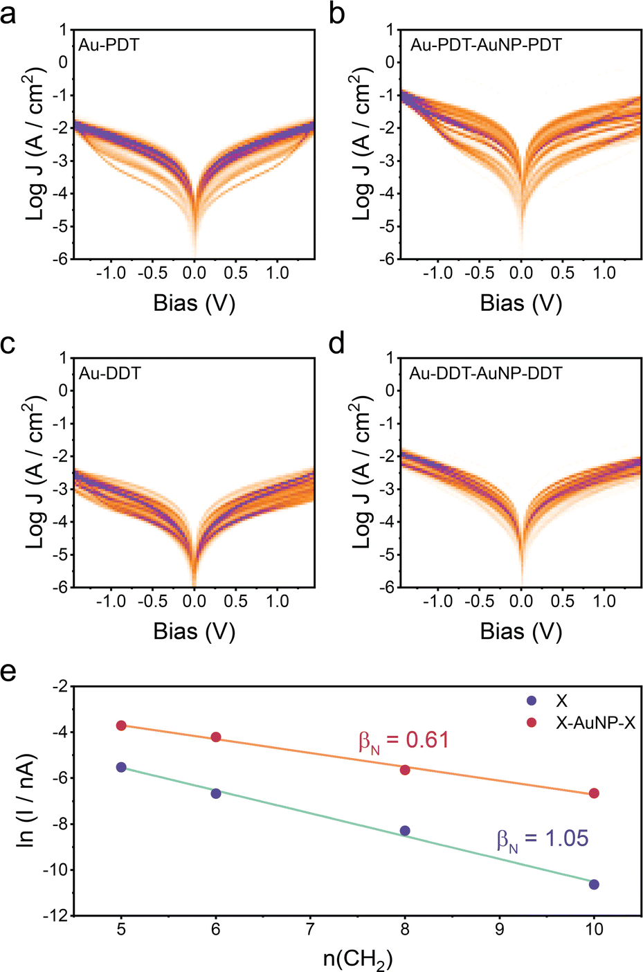 | ||
| Fig. 4 (a) 2D map of current density vs. bias voltage compiled from 1219 Au/1,5-pentanedithiol/Ga2O3/eGaIn junctions. (b) 2D map of current density vs. bias voltage compiled from 1590 Au/1,5-pentanedithiol/AuNPs/1,5-pentanedithiol/Ga2O3/eGaIn junctions. (c) 2D map of current density vs. bias voltage compiled from 1378 Au/1,10-decanedithiol/Ga2O3/eGaIn junctions. (d) 2D map of current density vs. bias voltage compiled from 1416 Au/1,10-decanedithiol/AuNPs/1,10-decanedithiol/Ga2O3/eGaIn junctions. (e) Natural logarithm of current versus n(CH2) for both the monolayer junction (purple) and the molecule/nanoparticle/molecule sandwiches (red). The solid lines are the linear fits, from which the attenuation factor β has been calculated. Data in (e) obtained from the respective 2D map at −600 mV. Maps in (a–d) compiled with 10 bins per decade and 50 bins per V. | ||
Finally, a topological origin to the enhanced conductance and reduced attenuation of the double layered structure arising from how the devices assemble or structure during the fabrication is considered. Alkanethiol SAMs, and to a lesser extent alkanedithiols, have been very well characterised by a multitude of surface science methods, including surface spectroscopies and probe microscopy. High coverage and well-ordered compact monolayers are formed, which in the case of alkanethiols are tilted approximately 30 degrees from the surface normal.34 Alkanedithiol SAMs have been used for the attachment of gold nanoparticles on-top of SAMs. In our case uncapped Au nanoparticles were attached from their freshly prepared solution in toluene, by incubating the monolayer dithiol SAM overnight in a solution of 8 ± 2 nm diameter GNPs. This was followed by immersion in the dithiol solution again to create the second layer. The steps of this fabrication protocol are visualised by deflection mode AFM in Fig. 5 for the 1,6-hexanedithiol system. At this imaging scale the first functionalisation step gives an apparently smooth and unstructured surface of the SAM-covered gold substrate (Fig. 5a). Statistical analysis of a 300 x 300 nm area taken from four different AFM topography maps, upon subtraction of a level plane, reveals a surface roughness (root-mean square) of 2.02 ± 0.66 nm. The image appearance dramatically changes when gold nanoparticles are adsorbed on-top of this SAM. The image of this structure (Fig. 5b) is much more structured and consistent with a disordered layer of GNPs sitting on the upper surface of the SAM. The same statistical analysis protocol returns a value for of 3.36 ± 0.96 nm as surface roughness. This is subsequently treated with 1,6-hexanedithiol (HDT) to form the Au–HDT–GNP–HDT structure (Fig. 5c). This image is distinctly less structured than the preceding step, the GNPs are not obviously visible, and surface roughness is significantly reduced to 2.31 ± 0.89 nm. From this, it is concluded that this second treatment with 1,6-hexanedithiol does not form a conformal layer mirroring the structure of the pre-adsorbed nanoparticles. On the contrary, there must be a large degree of restructuring as the nanoparticles are capped by the alkanedithiol layer, with partial intercalation between alkanedithiol sheaths on adjacent GNPs being possible. Thiols are known to form a compact and protective sheath around gold nanoparticles, which greatly stabilizes uncapped nanoparticles, and on account of their stability these monolayer capped GNPs have been referred to as monolayer-protected clusters.35 On account of the driving force for capping ligand shells to adsorb around the GNP core it is expected that a great degree of film restructuring would occur during the formation of the monolayer-protected nanoparticles within the film structure. The AFM imaging presented above shows that the nanoparticle sandwich film is non-uniform. This non-uniformity may arise from the nanoparticles sitting at somewhat different heights embedded in the film. There may also be conformational disordering of the ligand shell surrounding the nanoparticle, and this has been studied for alkanethiol capped gold nanocrystals with infrared spectroscopy. Infrared spectroscopic data from the literature does show evidence for a degree of disordering for alkanethiol capped gold nanoparticles, particularly for smaller chain length and cluster sizes,35–37 but chain ordering is dependent on other factors such as environment, compression of nanoparticle films and temperature (see ESI,‡ Section S3, for further discussion). Our preparation method in which nanoparticles are assembled on-top of monolayer alkanedithiol SAMs and then exposed “in situ” to the alkanedithiol to form the upper layer of the sandwich may be conducive to lower ordering than the standard process of forming monolayer capped nanoparticles in a solution environment. Further investigations comparing these different assembly protocols and their influence on order would be worthwhile.
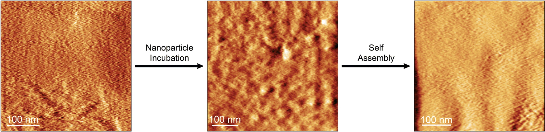 | ||
| Fig. 5 Deflection mode AFM images of: (A) The 1,6-hexanedithiol SAM monolayer, (B) 1,6-hexanedithiol monolayer following adsorption of GNPs and (C) the sandwich structure of 1,6-hexanedithiol-GNP-1,6-hexanedithiol. Image size is 400 × 400 nm (left), 500 × 500 nm (centre) and 450 × 450 nm (right). | ||
Electrical short-circuits in these devices made by the nanoparticles as an alternative explanation for the I–V behaviour has been ruled out since metallic transport characteristics are not observed in the device I–V curves. We can also discount an interpretation of our results based on a change of the wetting properties of the monolayer or on a different effective monolayer/eGaIn contact area being responsible for the observed charge transport properties. The former is discounted on account of similar interfacial chemistry being operative in the monolayer and the nanoparticle assembly devices, as an alkanedithiol monolayer is in both cases responsible for the contact with the eGaIn electrode. The latter is discounted on the basis of our topographic analysis, as the eGaIn electrode is coated by a rough Ga2O3 “skin”, that has been experimentally observed to wrinkle and buckle upon manipulation of the electrode and fabrication of the junctions.38 Even a pristine microdroplet of eGaIn (hence not having been manipulated and offering the smoothest Ga2O3 “skin” possible) has been demonstrated by AFM to have a surface roughness of ∼1 nm,39 therefore dominating in magnitude over the smaller ΔroughnessRMS (difference in roughness between the Au–monolayer and the Au–monolayer–NP-monolayer structures) of 0.29 nm observed between our devices. Therefore, while the effective contact area between the eGaIn electrode and the monolayer will indeed be lower than the calculated geometric contact area,38 no significant difference in their magnitude is expected between the pristine monolayers and the ML–GNP–ML assemblies.
A simple model is presented in the ESI‡ to offer a possible explanation for the disordered Au–ML–GNP–ML devices showing enhanced electrical conductance (also see the discussion of the model in Section S2 and Fig. S2 in the ESI‡). This topographic model assumes that there is a normal distribution of tunnelling distances of the GNPs to the enclosing electrodes. Since tunnelling current is not linear in distance this means that the longer and shorter distance do not balance out and a current enhancement results, which becomes larger as the distribution of tunnelling distances widens. Even small Ångstrom level modulations of the effective tunnelling distances can produce relatively large conductance enhancement within this model. This is of course a very simple model but shows how disorder in the placement of embedded nanoparticles and microscopic variation in the SAM structure might give rise to conductance enhancement of the device. There will be other factors such as the variation of SAM thickness and order at different faces of the GNPs, domain boundary and defect effects, and complex disorder. Another consideration is the structure and ordering of the linker molecules at the enclosing metal contact interfaces. The shapes and orientations of the nanoparticles will mean that the alkanedithiol capping ligands will meet at a wide variety of angles to the electrode contacts. This is clearly a very different scenario compared to a single SAM sandwiched perfectly between two model planar metal electrodes, which is a situation which might, for example, be approached with mercury drop contacts touching the top of SAMs.33 On the contrary if there is a prevalence of highly tilted linker molecules contacting the electrodes these might be expected to contribute to higher conductance for two reasons. First, if the SAM is highly tilted then the thickness will be relatively low, enhancing junction conductance. Second, it has been demonstrated at the single molecule level that highly tilted or compressed Au–molecule–Au junctions can exhibit significantly enhanced conductance.40,41
Conclusions
In summary, this study analyses the influence of introducing metal nanoparticles in double monolayer structures formed from SAMs and highlights the unexpected finding that the junction conductance is enhanced for these GNP–SAM double layer composite films. Restructuring of the films during the formation of the top SAM layer and the in situ formation of monolayer capped GNPs is believed to play a determining role in the conductance enhancement. The recorded electrical properties show no evidence for metallic short circuiting of the devices by the nanoparticles, hence showing the potential for the fabrication of large area devices which combine the electrical properties of nanoparticles and functional organic ligands.Materials and methods
All chemicals used in this study were purchased from Sigma-Aldrich (now Merck) and used without further purification. Solvents were purchased from ThermoFisher Scientific and used without further purification. Au substrates were purchased from Arrandee (200 nm Au/5 nm Cr/glass) and annealed with a butane torch before use, to promote (111) surface reconstruction. eGaIn was purchased from Sigma-Aldrich (now Merck), as 75.5% Ga, 24.5% In, 99.99 + % trace metal.The eGaIn apparatus was assembled using a microsyringe (ThermoScientific GasTight 10 μL) equipped with a tapered needle (SGE 26G, 0.11 mm inner diameter). The syringe is mounted on a Z translation stage (Thorlabs NanoFlex NFL5D + Thorlabs K-Cube Piezo Controller) which allows manual coarse approach and fine piezo-driven control. The substrate is mounted on a manual XY stage (2× Thorlabs XR25). The equipment is built on top of an optical table to reduce ambient vibration. A camera (Basler ACEPro) allows visual measurement of the contact area and calculation of the current density J. eGaIn conical tips were prepared by bifurcating a drop of eGaIn on a sacrificial area of the substrate.21 The tip was then moved to a pristine area of the substrate and driven into contact with the monolayer. A Keysight 33522B Arbitrary Waveform Generator (AWG) imposes an electrical bias to the sample (against ground), while the current from the tip is monitored with a transimpedance amplifier (Femto DLPCA-200). Data is acquired with a National Instrument PXI system (PXIe-1062Q chassis with a PXIe-4464 acquisition module and PXIe-PCIe8381 interface). Data acquisition and processing are performed with custom Labview VIs.
AFM imaging and carving/nanolithography were performed with a Keysight 5500 SPM system, equipped with a N9520A 9 μm scanner, operating in contact mode. NT-MDT CSG30 diving board cantilevers were employed, using a 0.3 nN setpoint for imaging and 20 nN for monolayer carving. Image processing and statistical analysis performed with Gwyddion 2.62.
Conflicts of interest
There are no conflicts to declare.Acknowledgements
This work was supported by EPSRC under Grants EP/M005046/1 (Single-Molecule Photo-Spintronics) and EP/M029522/1 (Single Molecule Plasmoelectronics). AV acknowledges funding from the Royal Society (University Research Fellowship URF\R1\191241). RJN also acknowledges funding from the Leverhulme Trust (grant RPG-2019-308).References
- L. Song, Y. Huang, Z. Nie and T. Chen, Macroscopic two-dimensional monolayer films of gold nanoparticles: fabrication strategies, surface engineering and functional applications, Nanoscale, 2020, 12(14), 7433–7460 RSC.
- C. E. McCold, Q. Fu, J. Y. Howe and J. Hihath, Conductance based characterization of structure and hopping site density in 2D molecule-nanoparticle arrays, Nanoscale, 2015, 7(36), 14937–14945 RSC.
- R. P. Andres, T. Bein, M. Dorogi, S. Feng, J. I. Henderson, C. P. Kubiak, W. Mahoney, R. G. Osifchin and R. Reifenberger, 'Coulomb staircase'' at room temperature in a self-assembled molecular nanostructure, Science, 1996, 272(5266), 1323–1325 CrossRef CAS.
- S. Kano, T. Tada and Y. Majima, Nanoparticle characterization based on STM and STS, Chem. Soc. Rev., 2015, 44(4), 970–987 RSC.
- E. Leary, H. Van Zalinge, S. J. Higgins, R. J. Nichols, F. F. de Biani, P. Leoni, L. Marchetti and P. Zanello, A molecular wire incorporating a robust hexanuclear platinum cluster, Phys. Chem. Chem. Phys., 2009, 11(25), 5198–5202 RSC.
- X. Roy, C. L. Schenck, S. Ahn, R. A. Lalancette, L. Venkataraman, C. Nuckolls and M. L. Steigerwald, Quantum Soldering of Individual Quantum Dots, Angew. Chem., Int. Ed., 2012, 51(50), 12473–12476 CrossRef CAS.
- C. L. Wu, X. H. Qiao, C. M. Robertson, S. J. Higgins, C. X. Cai, R. J. Nichols and A. Vezzoli, A Chemically Soldered Polyoxometalate Single-Molecule Transistor, Angew. Chem., Int. Ed., 2020, 59(29), 12029–12034 CrossRef CAS.
- S. E. F. Kleijn, S. C. S. Lai, M. T. M. Koper and P. R. Unwin, Electrochemistry of Nanoparticles, Angew. Chem., Int. Ed., 2014, 53(14), 3558–3586 CrossRef CAS.
- F. Fabrizi de Biani, C. Femoni, M. C. Iapalucci, G. Longoni, P. Zanello and A. Ceriotti, Redox Behavior of [H6-nNi38Pt6(CO)48]n- (n = 4–6) Anions: A Series of Metal Carbonyl Clusters Displaying Electron-Sink Features, Inorg. Chem., 1999, 38(16), 3721–3724 CrossRef CAS.
- S. E. Herrera, F. G. Davia, F. J. Williams and E. J. Calvo, Metal Nanoparticle Enhancement of Electron Transfer to Tethered Redox Centers through Self-Assembled Molecular Films, Langmuir, 2019, 35(19), 6297–6303 CrossRef CAS.
- P. S. Jensen, Q. Chi, F. B. Grumsen, J. M. Abad, A. Horsewell, D. J. Schiffrin and J. Ulstrup, Gold Nanoparticle Assisted Assembly of a Heme Protein for Enhancement of Long-Range Interfacial Electron Transfer, J. Phys. Chem. C, 2007, 111(16), 6124–6132 CrossRef CAS.
- H. Razzaq, R. Qureshi and D. J. Schiffrin, Enhanced rate of electron transfer across gold nanoparticle-anthraquinone hybrids, Electrochem. Commun., 2014, 39, 9–11 CrossRef CAS.
- A. Barfidokht, S. Ciampi, E. Luais, N. Darwish and J. J. Gooding, Distance-Dependent Electron Transfer at Passivated Electrodes Decorated by Gold Nanoparticles, Anal. Chem., 2013, 85(2), 1073–1080 CrossRef CAS.
- C. R. Bradbury, J. Zhao and D. J. Fermín, Distance-Independent Charge-Transfer Resistance at Gold Electrodes Modified by Thiol Monolayers and Metal Nanoparticles, J. Phys. Chem. C, 2008, 112(27), 10153–10160 CrossRef CAS.
- J.-N. Chazalviel and P. Allongue, On the Origin of the Efficient Nanoparticle Mediated Electron Transfer across a Self-Assembled Monolayer, J. Am. Chem. Soc., 2011, 133(4), 762–764 CrossRef CAS.
- J. Dyne, Y.-S. Lin, L. M. H. Lai, J. Z. Ginges, E. Luais, J. R. Peterson, I. Y. Goon, R. Amal and J. J. Gooding, Some More Observations on the Unique Electrochemical Properties of Electrode–Monolayer–Nanoparticle Constructs, Chem. Phys. Chem., 2010, 11(13), 2807–2813 CrossRef CAS.
- R. G. Freeman, K. C. Grabar, K. J. Allison, R. M. Bright, J. A. Davis, A. P. Guthrie, M. B. Hommer, M. A. Jackson, P. C. Smith, D. G. Walter and M. J. Natan, Self-Assembled Metal Colloid Monolayers - An Approach To SERS Substrates, Science, 1995, 267(5204), 1629–1632 CrossRef CAS.
- C. Jianrong, M. Yuqing, H. Nongyue, W. Xiaohua and L. Sijiao, Nanotechnology and biosensors, Biotechnol. Adv., 2004, 22(7), 505–518 CrossRef.
- M. Brust, D. Bethell, C. J. Kiely and D. J. Schiffrin, Self-Assembled Gold Nanoparticle Thin Films with Nonmetallic Optical and Electronic Properties, Langmuir, 1998, 14(19), 5425–5429 CrossRef CAS.
- S. Seo, B. Q. Viet, E. Hwang, Y. Cho, J. Lee, Y. Kawazoe and H. Lee, Nanoparticle Linker-Controlled Molecular Wire Devices Based on Double Molecular Monolayers, Small, 2019, 15(28), 1901183 CrossRef.
- R. C. Chiechi, E. A. Weiss, M. D. Dickey and G. M. Whitesides, Eutectic Gallium–Indium (EGaIn): A Moldable Liquid Metal for Electrical Characterization of Self-Assembled Monolayers, Angew. Chem., Int. Ed., 2008, 47(1), 142–144 CrossRef CAS.
- M. Brust, D. J. Schiffrin, D. Bethell and C. J. Kiely, Novel gold-dithiol nano-networks with non-metallic electronic properties, Adv. Mater., 1995, 7(9), 795–797 CrossRef CAS.
- J.-J. Yu, J. N. Ngunjiri, A. T. Kelley and J. C. Garno, Nanografting versus Solution Self-Assembly of α,ω-Alkanedithiols on Au(111) Investigated by AFM, Langmuir, 2008, 24(20), 11661–11668 CrossRef CAS.
- C. Vericat, M. E. Vela, G. Benitez, P. Carro and R. C. Salvarezza, Self-assembled monolayers of thiols and dithiols on gold: new challenges for a well-known system, Chem. Soc. Rev., 2010, 39(5), 1805 RSC.
- D. Fracasso, H. Valkenier, J. C. Hummelen, G. C. Solomon and R. C. Chiechi, Evidence for Quantum Interference in SAMs of Arylethynylene Thiolates in Tunneling Junctions with Eutectic Ga–In (EGaIn) Top-Contacts, J. Am. Chem. Soc., 2011, 133(24), 9556–9563 CrossRef CAS.
- L. Yuan, N. Nerngchamnong, L. Cao, H. Hamoudi, E. Del Barco, M. Roemer, R. K. Sriramula, D. Thompson and C. A. Nijhuis, Controlling the direction of rectification in a molecular diode, Nat. Commun., 2015, 6(1), 6324 CrossRef CAS.
- T. Wang, W. Du, N. Tomczak, L. Wang and C. A. Nijhuis, In Operando Characterization and Control over Intermittent Light Emission from Molecular Tunnel Junctions via Molecular Backbone Rigidity, Adv. Sci., 2019, 6(20), 1900390 CrossRef CAS.
- S. Park and H. J. Yoon, New Approach for Large-Area Thermoelectric Junctions with a Liquid Eutectic Gallium–Indium Electrode, Nano Lett., 2018, 18(12), 7715–7718 CrossRef CAS.
- C. A. Nijhuis, W. F. Reus and G. M. Whitesides, Molecular Rectification in Metal–SAM–Metal Oxide–Metal Junctions, J. Am. Chem. Soc., 2009, 131(49), 17814–17827 CrossRef CAS.
- W. F. Reus, M. M. Thuo, N. D. Shapiro, C. A. Nijhuis and G. M. Whitesides, The SAM, Not the Electrodes, Dominates Charge Transport in Metal-Monolayer//Ga2O3/Gallium–Indium Eutectic Junctions, ACS Nano, 2012, 6(6), 4806–4822 CrossRef CAS.
- G. I. Livshits, J. Bao, L. Sakamoto, T. Misaka, Y. Usami, Y. Otsuka and T. Matsumoto, Sacrificial gold coating enhances transport of liquid metal in pressurized fountain pen lithography, Sci. Rep., 2021, 11, 4670 CrossRef CAS.
- B. Xu and N. J. Tao, Measurement of Single-Molecule Resistance by Repeated Formation of Molecular Junctions, Science, 2003, 301(5637), 1221–1223 CrossRef CAS.
- R. E. Holmlin, R. Haag, M. L. Chabinyc, R. F. Ismagilov, A. E. Cohen, A. Terfort, M. A. Rampi and G. M. Whitesides, Electron Transport through Thin Organic Films in Metal–Insulator–Metal Junctions Based on Self-Assembled Monolayers, J. Am. Chem. Soc., 2001, 123(21), 5075–5085 CrossRef CAS.
- A. Ulman, Formation and Structure of Self-Assembled Monolayers, Chem. Rev., 1996, 96(4), 1533–1554 CrossRef CAS PubMed.
- A. C. Templeton, M. P. Wuelfing and R. W. Murray, Monolayer protected cluster molecules, Acc. Chem. Res., 2000, 33(1), 27–36 CrossRef CAS.
- B. Nieto-Ortega and T. Burgi, Vibrational Properties of Thiolate-Protected Gold Nanoclusters, Acc. Chem. Res., 2018, 51(11), 2811–2819 CrossRef CAS.
- M. J. Hostetler, J. J. Stokes and R. W. Murray, Infrared spectroscopy of three-dimensional self-assembled monolayers: N-alkanethiolate monolayers on gold cluster compounds, Langmuir, 1996, 12(15), 3604–3612 CrossRef CAS.
- F. C. Simeone, H. J. Yoon, M. M. Thuo, J. R. Barber, B. Smith and G. M. Whitesides, Defining the Value of Injection Current and Effective Electrical Contact Area for EGaIn-Based Molecular Tunneling Junctions, J. Am. Chem. Soc., 2013, 135(48), 18131–18144 CrossRef CAS.
- E. J. H. Soh, H. P. A. G. Astier, D. Daniel, J. Q. Isaiah Chua, A. Miserez, Z. Jia, L. Li, S. J. O’Shea, H. Bhaskaran, N. Tomczak and C. A. Nijhuis, AFM Manipulation of EGaIn Microdroplets to Generate Controlled, On-Demand Contacts on Molecular Self-Assembled Monolayers, ACS Nano, 2022, 16(9), 14370–14378 CrossRef CAS.
- W. Haiss, H. van Zalinge, D. Bethell, J. Ulstrup, D. J. Schiffrin and R. J. Nichols, Thermal gating of the single molecule conductance of alkanedithiols, Faraday Discuss., 2006, 131, 253–264 RSC.
- W. Haiss, C. S. Wang, I. Grace, A. S. Batsanov, D. J. Schiffrin, S. J. Higgins, M. R. Bryce, C. J. Lambert and R. J. Nichols, Precision control of single-molecule electrical junctions, Nat. Mater., 2006, 5(12), 995–1002 CrossRef CAS.
Footnotes |
| † Data collected using EPSRC funding at Liverpool are archived at https://doi.org/10.17638/datacat.liverpool.ac.uk/1853 |
| ‡ Electronic supplementary information (ESI) available. See DOI: https://doi.org/10.1039/d2cp05525b |
| This journal is © the Owner Societies 2023 |