
Gas-phase synthesis of nanoparticles: current application challenges and instrumentation development responses
Panagiotis
Grammatikopoulos
 *abc,
Theodoros
Bouloumis
d and
Stephan
Steinhauer
e
*abc,
Theodoros
Bouloumis
d and
Stephan
Steinhauer
e
aDepartment of Materials Sciences and Engineering, Guangdong Technion – Israel Institute of Technology, Shantou, Guangdong 515063, China. E-mail: panagiotis.g@gtiit.edu.cn
bGuangdong Provincial Key Laboratory of Materials and Technologies for Energy Conversion, Guangdong Technion – Israel Institute of Technology, Shantou, Guangdong 515063, China
cTechnion-Israel Institute of Technology, Haifa 32000, Israel. E-mail: panagiotisgr@technion.ac.il
dOkinawa Institute of Science and Technology (OIST) Graduate University, 1919-1 Onna-son, Okinawa 904-0495, Japan
eDepartment of Applied Physics, KTH Royal Institute of Technology AlbaNova University Center, Stockholm SE 106 91, Sweden
First published on 9th December 2022
Abstract
Nanoparticles constitute fundamental building blocks required in several fields of application with current global importance. To fully exploit nanoparticle properties specifically determined by the size, shape, chemical composition and interfacial configuration, rigorous nanoparticle growth and deposition control is needed. Gas-phase synthesis, in particular magnetron-sputtering inert-gas condensation, provides unique opportunities to realise engineered nanoparticles optimised for the desired use case. Here, we provide an overview of recent nanoparticle growth experiments via this technique, how the latter can meet application-specific requirements, and what challenges might impede the wide-spread adoption for scalable industrial synthesis. More specifically, we discuss the timely topics of energy, catalysis, and sensing applications enabled by gas-phase synthesised nanoparticles, as well as recently emerging advances in neuromorphic devices for unconventional computing. Having identified the most relevant challenges and limiting factors, we outline how advances in nanoparticle source instrumentation and/or in situ diagnostics can address current shortcomings. Eventually we identify common trends and directions, giving our perspective on the most promising and impactful applications of gas-phase synthesised nanoparticles in the future.
1. Introduction
Gas-phase synthesis of nanoparticles is a term that describes nanoparticle fabrication via nucleation and growth from a supersaturated atomic vapour which can be generated by various physical methods. It provides a solvent- and effluent-free technique to design monodisperse multifunctional nanoparticles with bespoke characteristics that can be subsequently soft-landed on or embedded in a desired substrate or device under ultra-high vacuum. Further, it is a versatile technique where one can satisfactorily control the physical structure and the chemical composition and ordering of fabricated nanoparticles by suitably fine-tuning a number of deposition parameters.Availing such possibilities, gas-phase synthesis has gained significant traction within the field of nanoparticle engineering. With magnetron-sputtering inert-gas condensation having been introduced almost three decades ago,1 the field is now well past its infancy, with numerous groups around the world obtaining or custom-building their cluster sources and deposition apparatuses, and engineering increasingly sophisticated nanoparticles (for example, utilising He nanodroplets for size-selected core–shell–(shell) particles2,3) of technological relevance (for example, in catalysis4). To manifest its coming-of-age, a subject-based textbook was published in 2017, with contributions by some of the pioneers and main current key players in the field.5 Two recent reviews on the subject, one by an author of the current perspective6 and one by the group at Castilla la Mancha7 focused on the growth of multi-elemental nanoparticles from a computational and an experimental viewpoint, respectively. Another two reviews by the Swansea group8 and Teer Coatings,9 on the other hand, focused on the technique's potential for catalysis and sensing applications.
With the current perspective, we aspire to provide a selective update on advances in the field; hence, for the most part we limit our bibliography within the past five years. Even as such, we do not provide a comprehensive review of what has happened within this period; instead, we distil recent literature and try to identify current challenges and corresponding developments that, in our opinion, formulate trends and determine directions for the near future. For example, while computational studies of the past decades primarily focused on the nucleation & growth processes,10–16 recent research is mostly zooming in on the fluid dynamics of the nanoparticle beam flow. Of course, several studies on the latter subject had been published before the examined period;17–19 however, it appears that this recent thrust is in full concord with simultaneous instrumentation advances in order to help resolve the very current challenge of limited nanoparticle yield (for example, see discussion on,20 below). In parallel, intense research over the past five years revolved around improving precision in structural control (down to the atomic level) predicted by atomistic simulations,21 obtained by source upgrades,22 and assessed by in situ diagnostics;23 therefore, these are the main themes of this perspective, with emphasis on the magnetron-sputtering inert-gas condensation technique.
2. Current application challenges
(a) Sensing
Research on nanoelectronic sensor devices employing gas-phase synthesised clusters and particles has been centred around strain sensing as well as chemical sensing of gaseous and bio- molecules. For a detailed review that also includes a broader scope of synthesis techniques, the reader is referred to reference.24 Here, we discuss selected recent examples emphasising specific aspects related to magnetron-sputtering inert-gas condensation. In general, two types of device configurations incorporating gas-phase synthesised nanoparticles can be distinguished: nanoparticle thin film assemblies and nanoparticle-decorated materials. While in the former case nanoparticles are responsible for sensor receptor as well as transducer function, in the latter case they only take on the role of the receptor, relying on other base materials for the transducer function. Most commonly, this results in different requirements and limitations related to the utilised nanoparticle synthesis method.Considering strain sensing, nanosensor devices can be constructed in a straight-forward manner by direct nanoparticle deposition onto pre-defined electrode contacts. The mechanical strain is transduced into a sensor signal via the electrical conductance of the nanoparticle film; to maximise sensitivity, it is highly advantageous to realise a nanoparticle layer close to percolation threshold. In this regard, magnetron-sputtering inert-gas condensation offers excellent opportunities due to the high level of nanoparticle coverage control by adjusting the deposition time, potentially with in situ electrical percolation monitoring. The significant potential of this approach was recently demonstrated in, for instance, Chen et al.25 An ultrahigh resolution pressure sensor was manufactured based on Pd nanoparticle layers on flexible PET membranes, resulting in a barometric altimeter with around 1 m resolution capable of detecting floor elevation inside a building elevator.
In the fields of chemical and bio-sensing, the particular appeal of employing gas-phase synthesis of nanoparticles stems from the solvent-free, “dry” deposition method that reduces surface contamination to a minimum. Analogous to strain sensing, nanoparticle films above the percolation limit can be used to transduce surface reactions into electrical signals. In particular, the sensor performance can be significantly enhanced via controlling the shape and morphology of the individual nanoparticles within the assembled layer.26 Such a combination of capabilities offered by magnetron-sputtering inert-gas condensation is rather unique to gas-phase synthesis methods. On the other hand, surface decoration/functionalisation of a conductive base material with gas-phase synthesised nanoparticles constitutes a highly attractive alternative to thin film-based devices. In this way, the sensitivity and selectivity of chemical and biosensors can be deliberately tuned via the nanoparticle interfaces by the choice of nanoparticle size, shape/morphology, chemical composition as well as degree of surface coverage and implantation level, while alleviating high nanoparticle yield requirements due to sub-monolayer coverages. Recent experimental work shows sensor property enhancements via nanoparticle decoration of thin films,27 nanoribbons,28 two-dimensional materials,29 and suspended nanowires,30 including ultrasmall size-selected nanoparticles31 as well multi-component alloyed particles32 with complex morphologies.33
(b) Catalysis
Synthesising materials ranging from nanoparticles tens of nm in diameter down to single-atom sites and controlling their interactions with their support have been the central theme in heterogeneous catalysis34 with a view to enabling gas- and liquid-phase catalytic reactions (including photocatalysis and electrocatalysis).35 Arguably the most potent feature of magnetron-sputtering inert-gas condensation for catalysis applications is rigorous mass (size) selection of the deposited clusters and nanoparticles, given the cluster source is typically coupled to a mass filter.Recent literature has demonstrated that such a capability can be used for realising excellent model systems for fundamental studies of catalytic processes, eventually leading to the development of enhanced catalyst materials. The oxygen evolution reaction in alkaline media was studied by Roy et al.,4 elucidating the fundamental properties of NiFeOxHy catalysts and the impact of nanoparticle size. The oxygen evolution reaction in acidic media was investigated by Zheng et al. utilising iridium–tantalum oxide catalysts with low noble-metal loading,36 demonstrating enhanced activity for cluster sizes below 2 nm. By relying on mass-selected Pt nanoparticles as model system for hydrogen evolution reaction in acidic media, Hansen et al. emphasised the importance of measuring intrinsic catalytic activities (turnover frequencies) to assess limiting processes and compare the catalytic activity of materials.37 Recently, Valtera et al. reported the controlled deposition of copper atoms and clusters containing 2–7 atoms and showed the remarkable catalytic activity of titania-supported copper tetramers as opposed to other cluster sizes and supports.38
These selected examples illustrate why mass selection during gas-phase nanoparticle deposition constitutes a most powerful tool for engineering new catalyst materials and understanding their properties. In addition, gas-phase synthesis has been used for the synthesis of bimetallic catalysts39 as well as for the realisation of nanostructured supports,40 validating further opportunities of the technique in this field. Despite such promising prospects, however, most real-world applications will remain out of reach due to low nanoparticle yield – a major limitation that needs to be particularly considered in the catalysis context.
(c) Energy
In energy-related applications such as solar energy conversion and energy storage, gas-phase synthesised nanomaterials have been widely employed (for a detailed review focusing on chemical vapour deposition and aerosol synthesis, see reference41), availing of tuneable properties along several lines. For the case of inert-gas condensation of nanoparticles, mainly three directions were recently investigated: first, materials for hydrogen storage have been devised, which, similar to sensing and catalysis applications, rely on the solid–gas interactions of engineered nanoparticles. For instance, Kumar et al. fabricated size-selected Pd nanoportals on underlying Mg films and, having used Density Functional Theory (DFT) calculations for the proof-of-concept, investigated the hydrogen flux through the nanoportals42 (the same simple concept was utilised later for single-nanoparticle electrochemistry43). Second, tailoring optical properties via the integration of nanoparticles was proposed for solar thermal collectors, which promise >90% light energy absorption,44 as well as perovskite-45 and silicon-46 based solar cells. These demonstrations showcase how the high degree of deposition parameter control during nanoparticle inert-gas condensation can be utilised for fine-tuning plasmonic absorption properties. Third, nanoparticle gas-phase deposition was recently utilised by Haro et al.47,48 to construct Si-based anodes for lithium-ion batteries. In that study, the nanoparticles were used as a scaffold that was instrumental to fabricating a specific arched nanoarchitecture of amorphous Si with optimised mechanical properties. Just like the aforementioned case of nanoparticulated Pd nanoribbons,28 a shadowing effect was used to fabricate a sculptured thin film; a concept that, in our opinion, has not been exploited to its full capacity from the gas-phase synthesis community yet.(d) Memristive devices and neuromorphic computing
Over the past two decades rapid advances in Machine Intelligence (MI) methods have made them ubiquitous components of our everyday lives. Powerful MI tools such as Artificial Neural Networks can perform complex tasks (e.g., image or speech recognition) much faster and more efficiently than conventional computational methods. However, the von Neumann architecture of conventional computers was not optimized for MI algorithms. This means that typical hardware upgrades cannot keep up with the ever-increasing requirements of massive MI algorithms. In addition, traditional computers are remarkably inefficient in terms of energy consumption when processing power-hungry data required for MI applications; a major shortcoming related to climate change issues which will only become more urgent as algorithms grow in size and complexity. As a result, new unconventional computation paradigms have recently emerged.Neuromorphic computing (or engineering) is such a new, promising paradigm based on integrated brain-like systems comprising electronic circuits that mimic neuron function in performing computations. MI methods are expected to greatly benefit from neuromorphic computing, and various schemes are currently being investigated as potential candidates for the required hardware.49 Due to the particular interest in this emerging field within diverse research communities, we aim at providing a more general introduction to the general principles in this topical area, facilitating the link with cluster-assembled device technology.
A device that has attracted strong attention as a primary unit for such systems is the memristor,50 a two-terminal structure that exhibits resistive switching, i.e., resistance tuning based on external stimuli such as voltage. Resistive switching can result in nonvolatile states where the device “memorises” the resistance state even after stimuli actions cease and can be, thus, used for writing/reading and storing information. As of today, the most popular configurations for building neuromorphic hardware based on memristors are (i) crossbar arrays,51 which offer the possibility for training an artificial neural network (ANN) locally on the array thus saving time and energy; (ii) spiking neural networks (SNN),52 which mimic neuron–synapse relationships to directly process information upon the arrival of binary events (spikes); (iii) and reservoir computing,53 which involves “reservoir” systems with short-term memory properties that can map inputs (mostly temporal signals) to high-dimensional systems using non-linear dynamics, resulting in decreased computational requirements. However promising these approaches are, memristive systems still need to address numerous challenges49 to achieve superior efficiency and speed compared with conventional hardware. Especially problematic seems to be the (re)programming of memristive devices, as well as the cycling endurance and reconfiguration of their properties beyond certain use.54
An exciting new direction emerged with the development of supersonic cluster beam deposition (SCBD),5 which enables the incorporation of nanoclusters into films and devices, with promising recent findings for implementation in neuromorphic computing. Specifically, the resistive switching on cluster-assembled thin films was demonstrated by Brown and co-workers55,56 on nanoparticulated films fabricated via SCBD close to the electrical percolation threshold, i.e., the condition where a fully connected network of nanoclusters starts forming (Fig. 1a). The resistive switching behaviour was attributed to the stochastic formation and destruction of nanojunctions (filament formation) between neighbouring clusters leading to conducting pathways of various lengths under the effect of applied voltage. This behaviour, recently investigated in depth via Ag nanoparticle networks,57 strongly resembles neuron firing signals, exhibiting brain-like long-range temporal correlations that are similarly measured in the cortex.58 Consecutively, Vahl et al.59 demonstrated the resistive switching property of individual Ag–Au and Ag–Pt alloy nanoparticles embedded in a thin SiO2 matrix by using the non-invasive conductive atomic force microscopy (C-AFM) technique. The flexibility of gas-phase synthesis allowed for controlled fabrication of nanoalloys, in order to limit the filament formation for acquiring reproducible switching characteristics. At the same time, limited filament formation contributed to the stability over many operation cycles. Remarkably, for the case of Ag–Pt thin film stack, the I–V measurement revealed resistive switching and a clear hysteresis loop even after 70 cycles (2 days) of constant “SET” and “RESET” applied voltages, despite the morphological alteration of the film's surface. In addition, reliable resistive switching in multi-stacks of Ag–Au and Ag–Pt (5 layers alternating with thin films of SiO2 of 2 and 4 nm, respectively) was demonstrated over multiple consecutive cycles with similar voltage values as the individual particles’ case. This clearly indicates the upscaling capability from the single nanoparticle level to multi-stack device with maintained electrical characteristics.
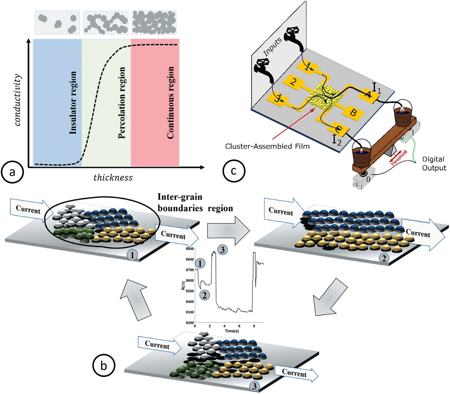 | ||
| Fig. 1 (a) Conductivity as a function of nanoparticulated film thickness, demonstrating clearly non-ohmic behaviour near the percolation threshold (see insets, above). (b) Resistive switching mechanism in cluster-assembled films beyond the percolation threshold. Different colours signify regions of different crystalline orientation. (c) Schematic representation of a receptron implemented through a nanoparticle-assembled film, developed in ref. 65. (a and b) reproduced from ref. 66; (c) reproduced from ref. 65, all under https://creativecommons.org/licenses/by/4.0/ (CC-BY 4.0). | ||
Very recently, resistive switching on Au cluster-assembled films was also observed beyond the percolation threshold accompanied by a non-ohmic behaviour.60 One would expect that as the thickness of the film increases beyond the percolation threshold the film should become more uniform and exhibit metal-like ohmic properties similar to the bulk material. However, cluster-assembled films have a very high number of grain boundaries due to the clusters widely maintaining their individual morphology, and, as a result, the electronic band structure is significantly modified, which seems to lead to very interesting and unexpected electrical and structural properties.61 The complex resistive switching in films beyond the percolation threshold is schematically explained in Fig. 1b; different colours indicate different crystalline orientations. As current flows through a region with random grain arrangement (1) there is local heating due to the Joule effect. This heating increases grain mobility, leading to rearrangement and reorientation of the grains which, in turn, leads to elimination of defects and/or grain sintering; thus, local resistance is decreased (2). Due to the decreased resistance, there is higher current density flowing through the structure, which causes even higher temperature increase and, thus, electrical connection breakdown between grains, leading to abrupt increase of resistance (3) and decrease of current density. The current density decrease allows for new electrical connections to form, leading back again to state (1). For a detailed study of the filament breakdown due to Joule heating, the reader is encouraged to look at the recent work by Wu et al.,62 based on molecular dynamics (MD) simulations. This dynamical reconfiguration creates the resistive switching and the spiking behaviour that is observed in ref. 61 for cluster-assembled films beyond the percolation threshold and can be easily tuned with external applied voltage based on the desired properties. An interesting parameter to be explored in such configurations of cluster-assembled films beyond the percolation threshold is the shape of the clusters. For nanocubes,26 for example, boundaries and defects could have a different effect on the resistive switching due to the nanocubes’ different filling factor and higher level of asymmetry, which would potentially give rise to a completely new behaviour. Further investigation showed that this dynamical reconfiguration of the clusters is fully reversible, and the resistive switching can even be observed at temperatures as low as 24 K,63 while it can also be modified with heating or cooling. Surprisingly, this cluster-assembled film exhibits negative temperature coefficient of resistance, which is not a characteristic of bulk metals. This was potentially attributed to the coexistence of space charge limited conduction and Coulomb blockade phenomena.
The applicability of cluster-assembled films for performing neuromorphic computations was demonstrated very recently with the fabrication of a proof-of-principle device based on a generalised perceptron model called receptron.64 As shown in the schematic illustration of Fig. 1c, a receptron-based device consists of a multielectrode configuration interconnected with a Au cluster-assembled film beyond the percolation threshold. By applying an initial voltage between two electrodes, e.g., 1-C, resistive switching behaviour across the film is triggered, leading to a certain configuration of conducting pathways while certain channels are “disabled” due to very low conductance (in the exemplar case, any channel having the B electrode as output). This way any input signal can be mapped in one of the two electrodes A or C, the equivalent of states 0 and 1, with the device acting essentially as binary classifier. When the input is binary the device can generate Boolean functions. This behaviour is based on the very high number of nanojunctions formed beyond a certain applied voltage-stimulus. The advantage of the receptron device is that the correct “weights” of the network need not be known a priori, which was the case for the perceptron model in typical ANNs, but instead are being determined based on the external stimuli-input. Once again, with a careful design this can result in a very efficient device for computational methods based on neuromorphic engineering: the question, however, remains whether a scalable device with extremely high numbers of input values can be fabricated and how large a resistive switching activation voltage it would require. For more technical details and remarkable findings, the interested reader is encouraged to study recent works in the topic.64,65
With this exciting, new field opening up, a plethora of new ideas is generated leading the current state-of-the-art towards disruptive technology applications. Vahl et al.67 demonstrated a prototype of a memsensor device, consisting of a memristive switching part and a sensing part, which can more accurately resemble biological systems that act upon sensing external stimuli. A memtransistor (three-terminal device) was also fabricated by Zhai et al.68 with the perspective to mimic neurosynaptic functions, offering better control (due to the third terminal) over the “learning” and “forgetting” stages of neuromorphic computing. Simultaneously, the first real-life neuromorphic applications have found their way into the health-care sector, with on-chip sensing of chronic obstructive pulmonary disease (COPD) from saliva samples.69 These applications though not yet based on cluster-assembled devices, are within the scope of gas-phase synthesis, especially given its suitability for sensing devices, as shown in the relevant section above.
3. Instrumentation development responses
(a) The need for yield: towards scalability in gas-phase synthesis of nanoparticles
With current nanotechnology applications becoming increasingly demanding in nanoparticle complexity and/or uniformity, even significant reduction in product mass is a price researchers are often willing to pay in order to gain good control of nanoparticle shapes and sizes. However, low material yields in research laboratory cluster sources prohibit the utilisation of gas-phase condensation techniques for massive nanoparticle production, an essential prerequisite for technology upscaling and adoption by industry.70 To make things worse, fabricated nanoparticles may go astray prior to their deposition, either by redeposition on the target or by decoration of the aggregation chamber walls,18 highlighting the method's wastefulness of materials. Related to this concern is also the inefficient utilisation of sputter-target material. In standard magnetron sputtering all sputtered matter comes from a circular-ring area of the target, concentric with it, due to the geometry of the plasma adjacent to the target. During sputtering a circular groove is formed while target material is consumed. As a result, typical values of the overall sputtered material of a fully used target do not exceed 5–10% of the total target mass. Clearly, innovations in instrumentation are required which focus on any of the nanoparticle deposition steps, i.e., the nucleation, growth, or transport; this is the subject of this section.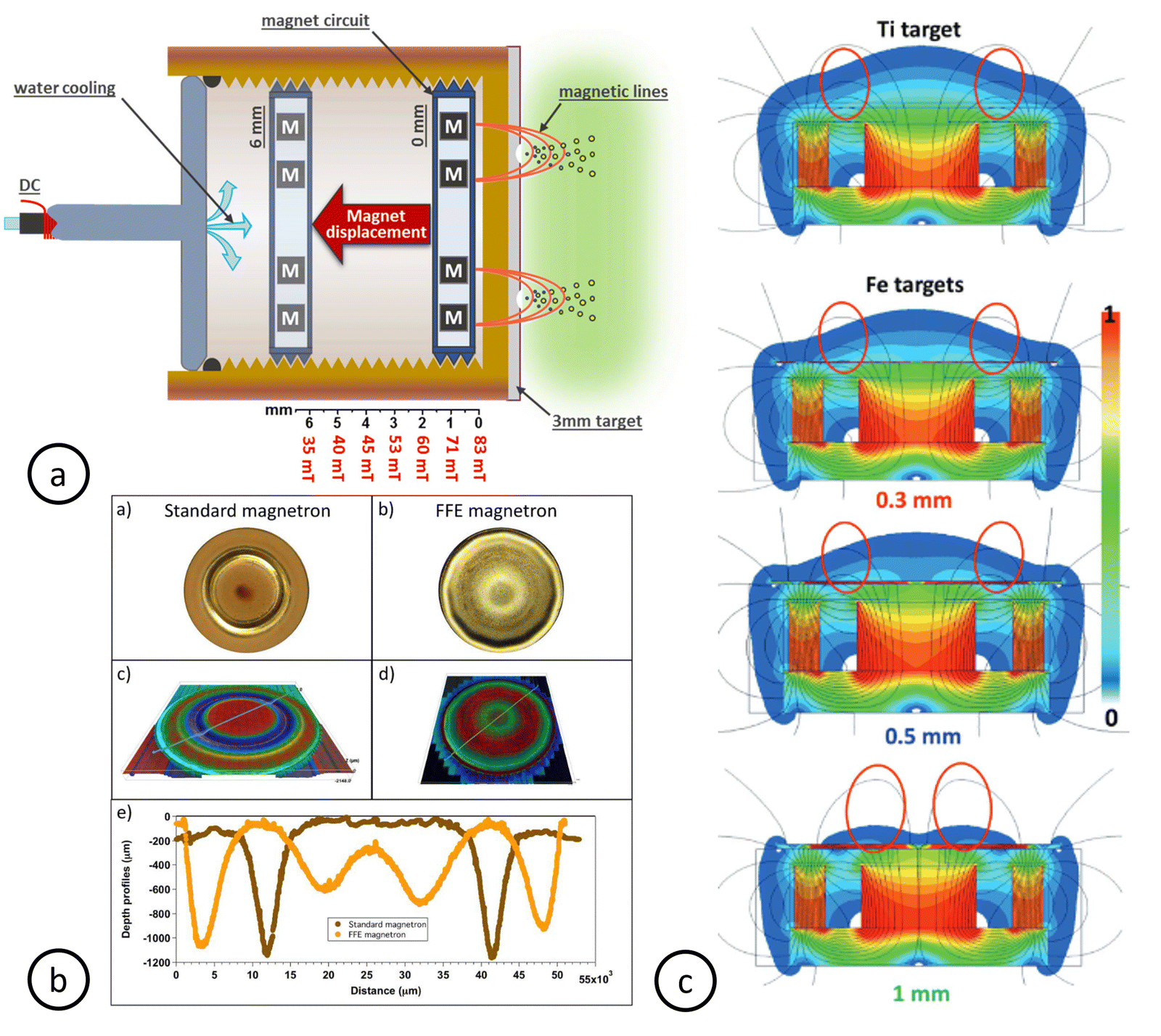 | ||
| Fig. 2 (a) Schematic representation of magnetron with an adjustable magnetic field. (b) Top row: Surface images illustrating differences in use between targets in standard magnetron (5%) and in an FFE magnetron (20%) Middle row: Corresponding microscope images of same targets. Bottom row: Depth profile comparison performed on lines indicated middle row images. (c) Finite element method (FEM) simulations of magnetron magnetic field applied to a paramagnetic Ti target (1 mm thickness) for comparison with three ferromagnetic Fe targets of various thicknesses, demonstrating the screening effect. (a) reproduced from ref. 71 with permission from John Wiley and Sons; (b) reproduced from ref. 72 with permission from Springer Nature; (c) reproduced from ref. 26 with permission from John Wiley and Sons. | ||
In a different approach, Huttel et al., in collaboration with Nano4Energy SLNE, recently introduced the Full Face Erosion (FFE) magnetron,72 which also utilises moving magnets, but parallel to the target and, most importantly, during deposition (a comparison between the FFE and a standard magnetron is shown in Fig. 2b). The concept of scanning the plasma over the whole target surface had already been used for conventional thin-film sputtering73,74 but required some technical adjustments for nanoparticle production. Indeed, with the FFE magnetron the overall target usage increased fourfold, reaching about 20% in weight consumption, as material was sputtered from the whole area of the target. More importantly, the avoidance of the aforementioned groove formation provides an additional advantage compared with standard magnetron guns. As was recently shown both experimentally and theoretically, the sputter yield at any given moment during sputtering is strongly affected by the incidence angle of the bombarding ions on the target surface.26,75 This means that, as the groove becomes deeper with usage time, this angle changes; so do the sputter yield and its resultant sputter-atom density near the target. As a result, inconsistencies occur in particle formation over time, leading to reduced control over nanoparticle configurations and compromised deposition uniformity and homogeneity. Doing away with groove formation, the FFE magnetron enables better control throughout the total nanoparticle fabrication process.
The possibility to fabricate monodisperse, uniform nanoparticles is of course important in its own right; however, it also has indirect consequences on the yield issue discussed here. Normally, size selection in gas-phase nanoparticle synthesis is always associated with post-growth separation, such as time-of-flight or quadrupole mass filtration.70,76 Generally speaking, mass filtration is a process designed to block certain objects or substances by some physical means, while letting others through; as such, it is by definition inevitable that output is always less in quantity than input. A method that succeeds in accurately determining nanoparticle sizes during growth, instead of producing a wide size dispersion first77,78 only to narrow it down by mass filtration afterwards, may help overcome this limitation.
Exploiting this principle, Vernieres et al. fabricated magnetic Fe nanocubes of tuneable structure;26 this system has attracted increasing attention in various applications, owing to enhanced activity and oxidation stability associated with cubic morphology.77–80 Considering that nanoparticle nucleation and growth happens close to the sputtering target, the authors utilised the high-permeability and resultant screening effect induced by their magnetic targets of various thicknesses to manipulate plasma confinement (Fig. 2c). In doing so, they introduced the target thickness as a crucial parameter that controls the density and temperature of sputtered atoms, producing nanoparticles of tailored size, shape, and crystallinity, and relieved the concept of nanoparticle size selection from the necessity to translate into mass filtration (thus reaching ten times higher material yield than with size-selected samples). In a similar approach, Zhu et al.81 investigated extensively the influence of backing plates on the strength of the magnetic field of the magnetron gun. By introducing Cu backing plates of various thicknesses between their non-magnetic Ge targets and the magnetron head, they could manipulate the magnetic field strength, which is inversely proportional to the plate thickness, and control the sizes of their fabricated Ge nanoparticles accordingly.
Another direction concerns the employment of cylindrical magnetrons, which is rising in popularity lately. The main idea is that the cylindrical geometry allows for (i) more efficient target usage, (ii) higher densities of sputtered atoms within the hollow target resulting in higher nanoparticle yields, (iii) improved size control by tuning the transfer gas flow accordingly and, thus, controlling dwell time, and (iv) a primary collimation of the nanoparticle beam even before exiting the target. Yet again, this is an old concept inherited by the nanoparticles community (e.g.,82) from conventional thin-film deposition.83 Several variations have been tried along the way; for example, while typical cylindrical magnetrons comprised of hollow cathodes, Tavares de Sá et al. proposed an inverse geometry involving a cylindrical hollow anode and a metallic rod along the axis as a cathode.84 More interestingly, the rod could be replaced by intertwined metallic wires availing the possibility to sputter nanoalloys with controllable nominal composition.
Newly proposed designs of cylindrical magnetrons combine their hollow geometry with concepts proposed for planar magnetrons as discussed above. For example, in their self-sustained hollow cathode sputtering source, Liu et al. installed a pair of magnets at the outlet of the hollow target to control the magnetic field and confine the plasma more efficiently.85 An iron ring was also placed in between the magnet and the hollow tube, separated from both by insulating plates. Their design led to a fourfold increase in nanoparticle yield and an even higher target utilisation rate increase (circa eighteen times), while enhancing the crystallisation of their nanoparticles. Even though it is unclear whether they were directly inspired by the aforementioned studies by Vernieres et al. or Zhu et al., their approach bares clear resemblance to the magnetic confinement concepts proposed by the latter for planar magnetrons. In an analogous fashion, more recently Nikitin et al. utilised a similar principle as the FFE by introducing their post cylindrical magnetron with a rotating magnetic circuit.86 The twist in their design was that the magnetic circuit, which was attached to a rotating spindle placed inside the magnetron, was rectangular, with the two different-length sides generating two elliptical magnetic tunnels shifted by 180°. Just like the FFE, target erosion was significantly reduced, maximising target usage and minimising possible related instabilities. Depending on the deposition conditions, they managed to increase their nanoparticle yield by ∼25–190% (depending on various considerations) compared with the planar magnetron configuration; further improved performance may be expected in future iterations.
Finally, a completely different approach to resolving the scale-up issue was proposed a few years ago with the Matrix Assembly Cluster Source (MACS), which traps atoms of a target material within a cryogenically solidified inert-gas matrix87 rather than condensing sputter atoms into clusters via collisions with inert-gas atomic vapour. Recently, successful deposition of elemental Au and Ag clusters on gram scale powders of TiO2 was reported for heterogeneous catalysis applications.88 The emission of clusters from MACS follows a process similar to the initial sputtering stage in magnetron sputtering with an inherent size control mechanism; as such it is promising for the industrial scale production of elemental homogeneous clusters. Further investigation is required regarding the production of nanoalloys or composite clusters, though.
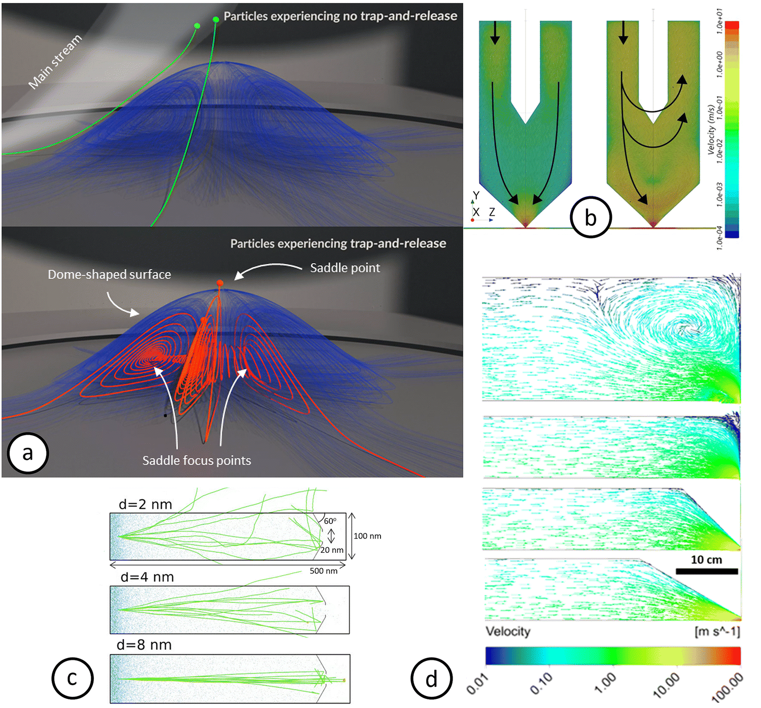 | ||
| Fig. 3 (a) Snapshots from Movie S2 (ESI of ref. 89) illustrating the difference in trajectory between particles experiencing the trap-and-release mechanism and particles which do not experience it. (b) Colour diagrams of the gas velocities simulated for different Ar flows at constant pressure (160 Pa) in a gas-aggregation source: (left) 40 sccm, orifice 2.5 mm and (right) 100 sccm, orifice 3.5 mm. For high Ar flux the flow becomes more complex and turbulent. (c) Drift trajectories of 2D NPs from MD simulations, 2, 4 and 8 nm in diameter (top to bottom). Smaller nanoparticles are more susceptible to Brownian motion and drift away from the beam axis, thus missing the orifice with a higher probability. (d) Gas velocity profiles inside the condensation chamber for four chamber geometries. Top: Cylindrical-wide (200 mm in diameter); second row: cylindrical-narrow (100 mm in diameter); third row: conical with a 90° apex; bottom: conical with a 60° apex. The optimal shape is the latter. (a) adapted from ref. 89 under https://creativecommons.org/licenses/by/4.0/ (CC-BY 4.0); (b) reproduced from ref. 86 with permission from John Wiley and Sons; (c) reproduced from ref. 90 under https://creativecommons.org/licenses/by/4.0/ (CC-BY 4.0); (d) reproduced from ref. 20 with permission from AIP Publishing. | ||
Moving further downstream inside the condensation chamber, Nikitin et al. used computational fluid dynamics (CFD) simulations to complement their experimental investigation of the effect of inert gas flow,86 and found that, for high Ar flux (100 sccm) the flow becomes more complex and turbulent, with vortices forming at different distances from the gas inlet (Fig. 3b). However, in situ observations with a quartz crystal microbalance (QCM) showed that the strong drag force from the carrier gas prevented the nanoparticles from decorating the chamber walls and resulted in higher deposition rates compared with those of a lower Ar flux (40 sccm). Another aspect related to the carrier gas fluid dynamics was investigated in the detailed study by Sanzone et al.20 In their study, they investigated the effect of the inlet position both by CFD and experimentally, and concluded that, ceteris paribus, carrier gas injected in the chamber from within the (planar) magnetron sputtering source produces higher cluster flux than when injected from the rear of the chamber. Naturally, different magnetrons, commercial or custom-built, have different configurations, and there may not be a one-size-fits-all geometry that maximises yield in all of them. However, the main message from this result holds true, with other similar configurations being tried, including multiple gas injection inlets around the target, which may also help collimate the nanoparticle beam.
In an attempt to bridge the vast gap, not only in scale but also in scope, between such CFD simulations and previous atomistic simulations on nucleation & growth,10–16 Zhao et al. simulated by large-scale 2D MD the nanoparticle flow throughout the whole condensation chamber all the way to the aperture.90 Using atomistic simulations enabled them to incorporate Brownian motion to the nanoparticle drag flow at a scale that had scarcely been approached in the past. They found that, with a standard nozzle geometry (20 nm aperture at 60° from the chamber walls), the probability of Au clusters to diverge significantly from their original straight trajectory and fail to exit the chamber significantly decreases with size, as the effect of Brownian collisions becomes weaker (Fig. 3c). Through this simulation, they were able to explain the experimental deposition of core-satellite Au complexes, where water molecules acted as the adhesive agent, safeguarding the stability of the system. Previously, Halder et al.91 had proposed a similar mechanism for the self-assembly of sub-nanometre Cu clusters; only in that case the agglomeration occurred on amorphous OH-terminated alumina support during CO2 conversion into methanol and hydrocarbons, and it was unstable since the Cu nanoassemblies disintegrated upon cooling down, due to the decrease of available water molecules.
Finally, Sanzone et al. went one step further and investigated the effect of the condensation chamber shape on the gas dynamics behaviour, also by CFD and experimentally.20 Comparing four chamber geometries (two cylindrical, one wide and one narrow, and two cylindrical with conical apexes of different angles, one of 90° and one of 60°), they concluded that the latter one is the most efficient (Fig. 3d). The narrow chamber shape and small apex angle effectively increased the carrier gas velocity near the chamber walls; as a result, the nanoparticles were less probable to attach to the walls and stayed on track toward a high-yield deposition on the sample support. In effect, this corresponds to the high carrier gas flux suggested by Nikitin et al. Nanoparticle yield obtained experimentally using the latter chamber configuration increased up to eight times (compared with the wide cylindrical chamber), and nanoparticle flux increased by around ten times.
(b) The need for control: towards atomically precise clusters
Nanoparticles can display unique physical and chemical properties. For instance, shape determines the type of surfaces of a nanoparticle, which, in turn, can dictate function (e.g., the ways atoms are arranged on the surface of a nanocatalyst can be decisive for an (electro-) chemical reaction). Moreover, in gas-phase synthesis the lack of ligands or other contaminants avail the formation of clean interfaces with the supports, providing a comparative advantage over chemical synthesis routes. However, precise engineering of clusters from the gas phase is no easy task, as it is purely physical mechanisms that determine their structure and resultant properties; one needs to simultaneously control both the energetics and kinetics of nucleation & growth with no surfactants present to direct the synthesis toward specific configurations. As a result, even though the fabrication of, e.g., nanoalloys by gas-phase synthesis has been technically possible for some time now, co-deposition of many elements is scarce, due the non-equilibrium processes it entails, with undecipherable kinetic factors often prevailing over energetics considerations. Therefore, it comes as no surprise that controlled synthesis of clusters or nanoparticles is key to exploiting their potential for the aforementioned applications; new strategies on how to achieve it are the subject of the current section.Charge transfer through the cluster–support interface is also of paramount importance for sensing or catalytic applications,30 and the choice of support can determine the utility (or lack of) of any certain nanosensor or nanocatalyst.31 For small clusters, the effect of the support is dual, since it can also determine the shape of the cluster and the configuration of the interface. In the aforementioned study by Valtera et al., where it was shown that clusters of different nuclearities display markedly different selectivity,38 an oscillatory behaviour in selectivity was observed between clusters with odd and even atom numbers. This was ascribed to the shape modifications induced by the interaction with the support, providing insights for potential research directions on controlling catalytic activity/selectivity via strain engineering through cluster–support interactions.
Such interactions are typically studied by DFT computer simulations; hence many studies combine experimental and theoretical findings. Interestingly, a similar odd–even oscillation was also reported via classical molecular dynamics (MD) for the potential energy of free-standing elemental clusters.21 Mattei et al. compared the independent nucleation of Au, Pt, and Pd clusters, and found that for Pd it is distinctly faster than for Au or (especially) Pt, which linger in dimeric cluster nuclei. Via simulated annealing of low-nuclearity clusters of all three elements they discovered oscillations in stability between small Au and Pt clusters containing odd and even numbers of atoms. Unlike their Pd counterparts, Au and Pt dimers and tetramers are more stable than trimers, which explains the observed stagnation in the experimental growth of Pt (mainly) and Au nanoparticles by magnetron-sputtering inert-gas condensation. This difference in stability was attributed to the different electronic structures of the three transition metals. Au and Pt have open-shell 6 s valence configurations (as opposed to 4d for Pd), leading toward alternating stable closed-shell and less-stable open-shell configurations for cluster seeds with even and odd atom numbers. Very recently, odd–even oscillations between open-closed electronic subshell configurations were also found to affect radiation cooling rates of Au clusters (and Au–Ag and Au–Pd binary nanoalloys).93 This effect could help stabilise particular multi-metallic cluster configurations in out-of-equilibrium gas-phase synthesis.
Pronounced differentiations in nucleation kinetics can determine the resultant configurations (in terms of size, shape, chemical ordering) of either elemental or mixed (if co-sputtered) nanoparticles; therefore, taking them into account when determining experimental conditions can give valuable insights. A recent example is the case of site-specific decoration of Fe nanocubes by Au atoms, reported by Vernieres et al.,94 where the more abundant and faster nucleating Fe atoms condensed into cubes about twice the edge length of concurrently grown Au clusters, with the latter eventually wetting the surface of the former toward multiple-frame Fe-Au cubic morphologies. The relative sizes of nascent elemental clusters that eventually form nanoalloys can, of course, also be controlled through appropriate instrumentation. Such is the case with sequential sputtering apparatuses,95 as recently explored by Hanuš et al. who fabricated Ni–Ti core–shell nanoparticles.96 The current limitation in this methodology concerns slowing down the cluster beam effectively enough via electrostatic lenses to allow for the formation of substantial shell thicknesses.
From all aspects of the discussion above, it is clear that a sufficient arsenal of in situ diagnostics methods would be expedient to inform future advances in source instrumentation and synthesis models; this is the subject of the next section.
A number of recent studies involved the in situ monitoring of the condensation near the target plane through suitably placed observation windows in the condensation chamber perpendicular to the cluster beam flow axis. Kousal et al.97 used Small Angle X-ray Scattering (SAXS) measurements from a synchrotron facility to investigate the growth of Cu nanoparticles (Fig. 4a). They witnessed that most of the growth occurred very near the target, and that a portion of the nascent nanoparticles was captured near the centre of the plasma ring (denoted the capture zone), where they grew very large (∼90 nm in diameter) due to the prolonged residence time. The rest of the particles were significantly smaller (∼10–20 nm in diameter) and escaped at an earlier stage forming the main cluster beam that was eventually deposited. The large particles were found to possess up to 100 electrical charges, which means their capture could be electrostatic in nature. The possibility of nascent clusters to carry both positive and negative charges during growth was demonstrated by Popok and Gurevich.98 on Ag particles using Electrostatic Quadrupole Mass Selection (EQMS); they also found that the fraction of multiply charged particles increased with size. A similar SAXS study again from the Biederman group in Prague, this time on Ag nanoparticle growth, revealed another two interesting observations.99 First, freshly grown clusters were redeposited on both the target itself and the chamber walls, a well-known fact caused by the high pressure inside the condensation chamber (compared with conventional film sputtering). Second, cycling oscillations occurred in deposited nanoparticle sizes and numbers, which was explained either on grounds of clusters being released from the capture zone only when a critical size was reached (due to electrostatic interactions) or of the nanoparticle cloud rotating about the magnetron axis along with the plasma and releasing particles periodically. Both explanations are worth investigating further, perhaps with the use of CFD simulations incorporating the gas inlet positions.
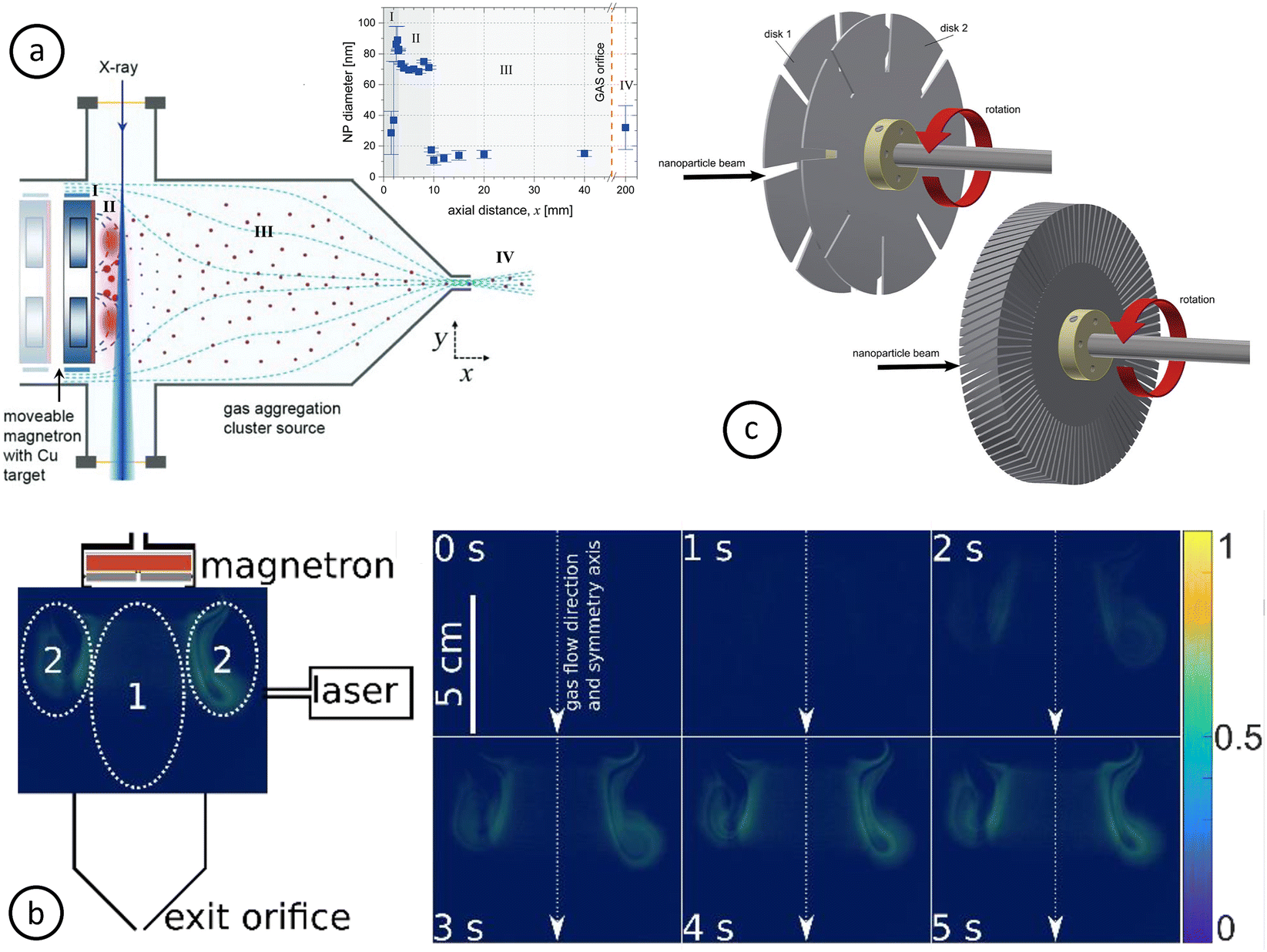 | ||
| Fig. 4 (a) Schematics of experimental setup for in situ SAXS measurements. Dashed blue lines indicate the magnetic field; light blue dotted lines indicate carrier gas flow. (b) Left panel: schematic representation of magnetron and orifice combined with an exemplary LLS image to indicate their relative positions. Three different regions are labelled inside the LLS image: edge regions (marked as 2) and centre region (marked as 1) Exemplar LLS images for a middle-inlet configuration (pressure 183 Pa, for 0 s, 1 s, 2 s, 3 s, 4 s and 5 s after plasma switch-on). The intensity is increasing with time, indicating nanoparticle growth, or increasing nanoparticle density, only in the edge regions. (c) Schematics of the nanoparticle time-of-flight filter rotors: (left) slotted disks (8 slits of angular width 5°, relative angle 9°, disk-to-disk distance 19 mm, disk thickness 1 mm); (right) helical rotor (90 slits of angular width 1°, relative angle 9°, total thickness 20 mm, printing resolution 0.2 mm). (a) reproduced from ref. 97 with permission from RSC; (b) reproduced from ref. 23 under https://creativecommons.org/licenses/by/4.0/ (CC-BY 4.0); (c) reproduced from ref. 104 with permission from Elsevier. | ||
Indeed, the latter was found to play the most important role in a very recent study by Drewes et al.23 probing the nanoparticle trapping very near the target with in situ Laser Light Scattering (LLS). Along with the gas inlet configuration, the inert gas (Ar) pressure was also found to determine the extent of trapping, which, in turn, affected the deposition rate and size distribution (Fig. 4b), indicating how in situ monitoring of the growth conditions may inform decisions regarding either optimal instrumentation design (e.g., inlet configurations) or sputtering parameters (e.g., Ar pressure). In a previous study, Drewes et al.100 also investigated the elemental composition of binary alloy nanoparticles by a combination of in operando Optical Emission Spectroscopy (OES) and X-ray Photoelectron Spectroscopy (XPS). In OES, the signal intensity is directly related to the number of excited atoms of each specific element; therefore, there is a correspondence between the intensity of OES lines and the concentration of each species. Utilising a composite target of Au rings embedded in the racetrack area of a Ag target and a similar observation geometry as in the SAXS studies discussed above, they also observed redeposition of sputtered material on the target. More specifically, they could identify distinct boundaries between regions of redepositions of each element, related to the plasma ring configuration adjacent to the target. Further, a significant target history effect was also clearly discernible, due to the redepositions. The temporal evolution of the phase separation of immiscible Ag–Cu nanoalloys was followed by another very recent study employing a combination of ex situ (Transmission Electron Microscopy, TEM) and in situ (optical spectroscopy, Grazing-Incidence Small- and Wide-angle X-ray Scattering, GISAXS/GIWAXS) methods,101 and deducing the effective diffusion coefficients of the two elements (confirming previous simulation results on the same102 and different systems103). The nanoparticles reported within this study are promising for potential anti-counterfeiting applications.
Finally, moving outside the condensation chamber, in two similar studies, Solař et al. utilized a very simple, 3D-printed mechanical time-of-flight filter to measure the velocities of Cu nanoparticles prior to being coated by sequential sputtering or to their deposition onto a support.104,105 Knowing the velocity distribution function of a cluster beam can be very important, as it may affect the final configuration in case of coating (e.g., core–shell vs. core-satellite), or the soft- or hard-landing upon deposition. However, previous attempts typically utilised electrostatic filters, which have the inherent limitation of not taking into account the aforementioned multiplicity in electrical charge carried by the nanoparticles in the beam. Instead, the newly proposed filter is based simply on geometry; two variants were proposed (Fig. 4c), one containing slotted disks (where the measurement parameters are the rotation velocity, the disc separation, and the slot angles) and one containing a helical rotor of a certain width (20 mm), number of slits (90) and slit angle (9°). Since a direct dependence of nanoparticle velocity with their size was revealed, the proposed velocity filter may also be useful as a mass filter; to this end, further corroboration of this dependence is required for other systems, as well.
4. Conclusions and outlook
The first part of this perspective revolved around a broad range of recent advances in various applications, from those traditionally associated with nanoparticle technologies such as sensing, catalysis, and energy, to emerging neuromorphic computing, a new, highly ambitious direction that may benefit from the use of nanoparticles. Next, we presented relevant experimental developments addressing challenges related to these applications. We identified the need for increased nanoparticle yield and precise structural control as the most crucial requirements for industrial employment of nanotechnologies invented in the laboratory and presented recent strategies to achieve these goals by appropriate instrumentation upgrade by in situ diagnostics and large-scale simulations of nanoparticle beam flows.With our approach we tried to directly connect application needs to corresponding responses. For example, good control and monitoring of the deposition process is useful to allow stopping just prior to or immediately after percolation for sensing or neuromorphic computing, a challenge addressed by the development of in situ diagnostic tools; the fabrication of configuration-sensitive sub-nanometre clusters for sensors or catalysts, on the other hand, necessitates precise control and assessment of nucleation & growth during deposition. For catalytic or energy applications at an industrial scale, large amounts of nanoparticles are necessary (e.g., to decorate collector sheets for battery anodes); hence the importance for production scale-up.
While reviewing recent literature, we identified a lack of a cohesive narrative covering various aspects of the synthesis process, from the nucleation & growth stages to deposition and device fabrication. This is in spite of overlapping or complementary studies often corroborating each other. The aspiration of this perspective is to help create such a general narrative regardless of differences between various instruments around the world. To this end, we added comments and relevant discussion about potential future experiments or general directions. We found that the adoption of concepts from regular film deposition proved useful, as expected, for modifying cluster source systems or for better understanding growth mechanisms; it may also be a source of further inspiration in the future. Also, that simple ideas can go a long way, either in terms of instrumentation (e.g., mechanical time-of-flight filter) or in terms of deposition strategies (e.g., sculptured thin films via nanoparticle shadowing effect).
In closing, we would like to highlight that – despite being seen as not en vogue anymore by some – nanotechnology and nanoparticles in particular are central elements for tackling major global issues, including (renewable) energy as well as environmental sensing and remediation. Furthermore, we would like to stress the potential of unconventional computation, which may still be in an earlier development stage, but increasingly receives generous support from both the public sector and angel investment.106 Utilisation of gas-phase synthesised nanoparticles for relevant solid-state devices had been sporadically proposed in the past, but over the past five years its potential to facilitate disruptive technologies routed to become dominant has become increasingly apparent.
Conflicts of interest
The authors declare no conflict of interest.Acknowledgements
Work performed at GTIIT was supported by funding from the Guangdong Technion Israel Institute of Technology. S. S. acknowledges support from the Swedish Research Council for Sustainable Development (Formas, grant number 2019-01353). T.B acknowledges funding from JSPS for the KAKENHI Grants-in-Aid for Scientific Research (Grant No. 22J10196). The authors are grateful to Pavel Puchenkov from OIST's Scientific Computing and Data Analysis section for designing and providing the Table of Contents graphic.References
- H. Haberland, M. Mall, M. Moseler, Y. Qiang, T. Reiners and Y. Thurner, Filling of micron-sized contact holes with copper by energetic cluster impact, J. Vac. Sci. Technol., A, 1994, 12(5), 2925 CrossRef.
- J. P. Toennies and A. F. Vilesov, Superfluid helium droplets: a uniquely cold nanomatrix for molecules and molecular complexes, Angew. Chem., Int. Ed., 2004, 43, 2622 CrossRef.
- A. Boatwright, C. Feng, D. Spence, E. Latimer, C. Binns, A. M. Ellis and S. Yang, Helium droplets: a new route to nanoparticles, Faraday Discuss., 2013, 162, 113 RSC.
- C. Roy, B. Sebok, S. B. Scott, E. M. Fiordaliso, J. E. Sørensen, A. Bodin, D. B. Trimarco, C. D. Damsgaard, P. C. K. Vesborg, O. Hansen, I. E. L. Stephens, J. Kibsgaard and I. Chorkendorff, Impact of nanoparticle size and lattice oxygen on water oxidation on NiFeOxHy, Nat. Catal., 2018, 1, 820 CrossRef.
- Gas-Phase Synthesis of Nanoparticles, ed. Y. Huttel, Wiley-VCH, Weinheim, 2017 Search PubMed.
- P. Grammatikopoulos, Atomistic modeling of the nucleation and growth of pure and hybrid nanoparticles by cluster beam deposition, Curr. Opin. Chem. Eng., 2019, 23, 164 CrossRef.
- R. López-Martín, B. Santos Burgos, P. S. Normile, J. A. De Toro and C. Binns, Gas phase synthesis of multi-element nanoparticles, Nanomaterials, 2021, 11, 2803 CrossRef.
- R. E. Palmer, R. Cai and J. Vernieres, Synthesis without solvents: the cluster (nanoparticle) beam route to catalysts and sensors, Acc. Chem. Res., 2018, 51, 2296 CrossRef CAS PubMed.
- G. Sanzone, J. Yin and H. Sun, Scaling up of cluster beam deposition technology for catalysis application, Front. Chem. Sci. Eng., 2021, 15(6), 1360 CrossRef CAS.
- F. Baletto, C. Mottet and R. Ferrando, Microscopic mechanisms of the growth of metastable silver icosahedra, Phys. Rev. B: Condens. Matter Mater. Phys., 2001, 63, 155408 CrossRef.
- E. Quesnel, E. Pauliac-Vaujour and V. Muffato, Modelling metallic nanoparticle synthesis in a magnetron-based nanocluster source by gas condensation of a sputtered vapor, J. Appl. Phys., 2010, 107, 054309 CrossRef.
- C. Cassidy, V. Singh, P. Grammatikopoulos, F. Djurabekova, K. Nordlund and M. Sowwan, Inoculation of silicon nanoparticles with silver atoms, Sci. Rep., 2013, 3, 3083 CrossRef.
- V. Singh, C. Cassidy, P. Grammatikopoulos., F. Djurabekova, K. Nordlund and M. Sowwan, Heterogeneous gas-phase synthesis and molecular dynamics modeling of Janus and core-satellite Si-Ag nanoparticles, J. Phys. Chem. C, 2014, 118, 13869 CrossRef CAS.
- J. Zhao, E. Baibuz, J. Vernieres, P. Grammatikopoulos, V. Jansson, M. Nagel, S. Steinhauer, M. Sowwan, A. Kuronen, K. Nordlund and F. Djurabekova, Formation mechanism of Fe nanocubes by magnetron sputtering inert gas condensation, ACS Nano, 2016, 10, 4684 CrossRef CAS.
- M. Bohra, P. Grammatikopoulos, V. Singh, J. Zhao, E. Toulkeridou, S. Steinhauer, J. Kioseoglou, J.-F. Bobo, K. Nordlund, F. Djurabekova and M. Sowwan, Tuning the onset of ferromagnetism in heterogeneous bimetallic nanoparticles by gas phase doping, Phys. Rev. Mater., 2017, 1, 066001 CrossRef.
- H. Akbarzadeh, A. N. Shamkhali and E. Mehrjouei, Ag–Au bimetallic nanoclusters formed from a homogeneous gas phase: a new thermodynamic expression confirmed by molecular dynamics simulation, Phys. Chem. Chem. Phys., 2017, 19, 3763 RSC.
- X. Wang, F. E. Kruis and P. H. McMurry, Aerodynamic focusing of nanoparticles: I. Guidelines for designing aerodynamic lenses for nanoparticles, Aerosol. Sci. Tech., 2005, 39(7), 611 CrossRef CAS.
- P. V. Kashatanov, B. M. Smirnov and R. Hippler, Magnetron plasma and nanotechnology, Phys Usp, 2007, 50, 455 CrossRef.
- B. M. Smirnov, Processes involving clusters and small particles in a buffer gas, Phys Usp, 2011, 54, 691 CrossRef CAS.
- G. Sanzone, J. Yin, K. Cooke, H. Sun and P. Lievens, Impact of the gas dynamics on the cluster flux in a magnetron cluster-source: Influence of the chamber shape and gas-inlet position, Rev. Sci. Instrum., 2021, 92, 033901 CrossRef CAS PubMed.
- J.-G. Mattei, P. Grammatikopoulos, J. Zhao, V. Singh, J. Vernieres, S. Steinhauer, A. Porkovich, E. Danielson, K. Nordlund, F. Djurabekova and M. Sowwan, Gas-phase synthesis of trimetallic nanoparticles, Chem. Mater., 2019, 31, 2151 CrossRef CAS.
- C. Yin, E. Tyo, K. Kuchta, B. von Issendorff and S. Vajda, Atomically precise (catalytic) particles synthesized by a novel cluster deposition instrument, J. Chem. Phys., 2014, 140, 174201 CrossRef CAS PubMed.
- J. Drewes, S. Rehders, T. Strunskus, H. Kersten, F. Faupel and A. Vahl, In situ laser light scattering for temporally and locally resolved studies on nanoparticle trapping in a gas aggregation source, Part. Part. Syst. Charact., 2022, 2200112 CrossRef CAS.
- E. Skotadis, E. Aslanidis, M. Kainourgiaki and D. Tsoukalas, Nanoparticles synthesised in the gas-phase and their applications in sensors: A review, Appl. Nano., 2020, 1(1), 70 CrossRef.
- M. Chen, W. Luo, Z. Xu, X. Zhang, B. Xie, G. Wang and M. Han, An ultrahigh resolution pressure sensor based on percolative metal nanoparticle arrays, Nat. Commun., 2019, 10, 4024 CrossRef.
- J. Vernieres, S. Steinhauer, J. Zhao, A. Chapelle, P. Menini, N. Dufour, R. E. Diaz, K. Nordlund, F. Djurabekova, P. Grammatikopoulos and M. Sowwan, Gas phase synthesis of multifunctional Fe-based nanocubes, Adv. Funct. Mater., 2017, 27, 1605328 CrossRef.
- V. Postica, A. Vahl, D. Santos-Carballal, T. Dankwort, L. Kienle, M. Hoppe, A. Cadi-Essadek, N. H. de Leeuw, M.-I. Terasa, R. Adelung, F. Faupel and O. Lupan, Tuning ZnO sensors reactivity toward volatile organic compounds via Ag doping and nanoparticle functionalization, ACS Appl. Mater. Interfaces, 2019, 11(34), 31452 CrossRef PubMed.
- E. H. Sánchez, P. S. Normile, J. A. De Toro, R. Caballero, J. Canales-Vázquez, E. Rebollar, M. Castillejo and J. M. Colino, Flexible, multifunctional nanoribbon arrays of palladium nanoparticles for transparent conduction and hydrogen detection, Appl. Surf. Sci., 2019, 470, 212 CrossRef.
- E. Danielson, V. A. Sontakke, A. J. Porkovich, Z. Wang, P. Kumar, Z. Ziadi, Y. Yokobayashi and M. Sowwan, Graphene based field-effect transistor biosensors functionalized using gas-phase synthesized gold nanoparticles, Sens. Actuators, B, 2020, 320(1), 128432 CrossRef.
- A. Porkovich, Z. Ziadi, P. Kumar, J. Kioseoglou, N. Jian, L. Weng, S. Steinhauer, J. Vernieres, P. Grammatikopoulos and M. Sowwan, In situ observation of metal to metal oxide progression: A study of charge transfer phenomenon at Ru-CuO interfaces, ACS Nano, 2019, 13(11), 12425 CrossRef.
- S. Steinhauer, E. Lackner, F. Sosada-Ludwikowska, V. Singh, J. Krainer, R. Wimmer-Teubenbacher, P. Grammatikopoulos, A. Köck and M. Sowwan, Atomic-scale structure and chemical sensing application of ultrasmall size-selected Pt nanoparticles supported on SnO2, Mater. Adv., 2020, 1, 3200 RSC.
- A. Vahl, O. Lupan, D. Santos-Carballal, V. Postica, S. Hansen, H. Cavers, N. Wolff, M.-I. Terasa, M. Hoppe, A. Cadi-Essadek, T. Dankwort, L. Kienle, N. H. de Leeuw, R. Adelung and F. Faupel, Surface functionalization of ZnO:Ag columnar thin films with AgAu and AgPt bimetallic alloy nanoparticles as an efficient pathway for highly sensitive gas discrimination and early hazard detection in batteries, J. Mater. Chem. A, 2020, 8, 16246 RSC.
- S. Steinhauer, J. Vernieres, J. Krainer, A. Köck, P. Grammatikopoulos and M. Sowwan, In situ chemoresitistive sensing in the environmental TEM: Probing functional devices and their nanoscale morphology, Nanoscale, 2017, 9, 7380 RSC.
- Z. Li, S. Ji, Y. Liu, X. Cao, S. Tian, Y. Chen, Z. Niu and Y. Li, Well-defined materials for heterogeneous catalysis: From nanoparticles to isolated single-atom sites, Chem. Rev., 2020, 120(2), 623 CrossRef PubMed.
- L. Liu and A. Corma, Metal catalysts for heterogeneous catalysis: From single atoms to nanoclusters and nanoparticles, Chem. Rev., 2018, 118(10), 4981 CrossRef.
- Y.-R. Zheng, J. Vernieres, Z. Wang, K. Zhang, D. Hochfilzer, K. Krempl, T.-W. Liao, F. Presel, T. Altantzis, J. Fatermans, S. B. Scott, N. M. Secher, C. Moon, P. Liu, S. Bals, S. Van Aert, A. Cao, M. Anand, J. K. Nørskov, J. Kibsgaard and I. Chorkendorff, Monitoring oxygen production on mass-selected iridium–tantalum oxide electrocatalysts, Nat. Energy, 2022, 7, 55 CrossRef.
- J. N. Hansen, H. Prats, K. K. Toudahl, N. M. Secher, K. Chan, J. Kibsgaard and I. Chorkendorff, Is there anything better than Pt for HER?, ACS Energy Lett., 2021, 6(4), 1175 CrossRef PubMed.
- S. Valtera, J. Jašik, M. Vaidulych, J. E. Olszówka, M. Zlámalová, H. Tarábková, L. Kavan and Š. Vajda, Atom by atom built subnanometer copper cluster catalyst for the highly selective oxidative dehydrogenation of cyclohexene, J. Chem. Phys., 2022, 156, 114302 CrossRef PubMed.
- F. R. Negreiros, A. Halder, C. Yin, A. Singh, G. Barcaro, L. Sementa, E. C. Tyo, M. J. Pellin, S. Bartling, K.-H. Meiwes-Broer, S. Seifert, P. Sen, S. Nigam, C. Majumder, N. Fukui, H. Yasumatsu, S. Vajda and A. Fortunelli, Bimetallic Ag–Pt sub-nanometer supported clusters as highly efficient and robust oxidation catalysts, Angew. Chem., 2018, 57(5), 1209 CrossRef PubMed.
- A. Halder, C. Lenardi, J. Timoshenko, A. Mravak, B. Yang, L. K. Kolipaka, C. Piazzoni, S. Seifert, V. Bonačiċ-Kouteckẏ, A. I. Frenkel, P. Milani and S. Vajda, CO2 methanation on Cu-cluster decorated zirconia supports with different morphology: A combined experimental in situ GIXANES/GISAXS, ex situ XPS and theoretical DFT study, ACS Catal., 2021, 11(10), 6210 CrossRef CAS.
- H. Zhang, H. Zhou, Y. Wang, S. Li and P. Biswas, Mini review on gas-phase synthesis for energy materials, Energy Fuels, 2021, 35(1), 63 CrossRef.
- S. Kumar, T. Pavloudis, V. Singh, H. Nguyen, S. Steinhauer, C. Pursell, B. Clemens, J. Kioseoglou, P. Grammatikopoulos and M. Sowwan, Hydrogen flux through size selected Pd nanoparticles into underlying Mg nanofilms, Adv. Energy Mater., 2018, 8(4), 170326 Search PubMed.
- A. Datta, A. J. Porkovich, P. Kumar, G. Nikoulis, J. Kioseoglou, T. Sasaki, S. Steinhauer, P. Grammatikopoulos and M. Sowwan, Single nanoparticle activities in ensemble: A study on Pd cluster nanoportals for electrochemical oxygen evolution reaction, J. Phys. Chem. C, 2019, 123, 26124 CrossRef.
- N. Perdana, J. Drewes, F. Pohl, A. Vahl, T. Strunskus, M. Elbahri, C. Rockstuhl and F. Faupel, A thin-film broadband perfect absorber based on plasmonic copper nanoparticles, Micro Nano Eng., 2022, 16, 100154 CrossRef.
- M. Caleffi, P. Mariani, G. Bertoni, G. Paolicelli, L. Pasquali, A. Agresti, S. Pescetelli, A. Di Carlo, V. De Renzi and S. D’Addato, Ag/MgO nanoparticles via gas aggregation nanocluster source for perovskite solar cell engineering, Materials, 2021, 14(19), 5507 CrossRef.
- S. Marom, M. Dorresteijn, R. Modi, A. Podestà and M. Di Vece, Silver nanoparticles from a gas aggregation nanoparticle source for plasmonic efficiency enhancement in a-Si solar cells, Mater. Res. Express, 2019, 6, 045012 CrossRef.
- M. Haro, V. Singh, S. Steinhauer, E. Toulkeridou, P. Grammatikopoulos and M. Sowwan, Nanoscale heterogeneity of multilayered Si anodes with embedded nanoparticle scaffolds for Li-ion batteries, Adv. Sci., 2017, 4(10), 1700180 CrossRef.
- M. Haro, P. Kumar, J. Zhao, P. Koutsogiannis, A. J. Porkovich, Z. Ziadi, T. Bouloumis, V. Singh, E. J. Juarez-Perez, E. Toulkeridou, K. Nordlund, F. Djurabekova, M. Sowwan and P. Grammatikopoulos, Nano-vault architecture mitigates stress in silicon-based anodes for lithium-ion batteries, Commun. Mater., 2021, 2, 16 CrossRef CAS.
- D. Joksas, A. Al Mutairi, O. Lee, M. Cubukcu, A. Lombardo, H. Kurebayashi, A. J. Kenyon and A. Mehonic, Memristive, spintronic, and 2D-materials-based devices to improve and complement computing hardware, Adv. Intell. Syst., 2022, 4, 2200068 CrossRef.
- D. Ielmini and R. Waser, Resistive Switching: From Fundamentals of Nanoionic Redox Processes to Memristive Device Applications, John Wiley & Sons, Hoboken, NJ, 2015 Search PubMed.
- C. Li, M. Hu, Y. Li, H. Jiang, N. Ge, E. Montgomery, J. Zhang, W. Song, N. Dávila, C. E. Graves, Z. Li, J. P. Strachan, P. Lin, Z. Wang, M. Barnell, Q. Wu, R. S. Williams, J. J. Yang and Q. Xia, Analogue signal and image processing with large memristor crossbars, Nat. Electronics, 2018, 1, 52 CrossRef.
- J. Pei, L. Deng, S. Song, M. Zhao, Y. Zhang, S. Wu, G. Wang, Z. Zou, Z. Wu, W. He, F. Chen, N. Deng, S. Wu, Y. Wang, Y. Wu, Z. Yang, C. Ma, G. Li, W. Han, H. Li, H. Wu, R. Zhao, Y. Xie and L. Shi, Towards artificial general intelligence with hybrid Tianjic chip architecture, Nature, 2019, 572, 106 CrossRef.
- Y. Zhong, J. Tang, X. Li, B. Gao, H. Qian and H. Wu, Dynamic memristor-based reservoir computing for high-efficiency temporal signal processing, Nat. Commun., 2021, 12, 408 CrossRef PubMed.
- A. P. James and L. O. Chua, Analog neural computing with super-resolution memristor crossbars, IEEE Transactions on Circuits and Systems I: Regular Papers, 2021, 68(11), 4470 Search PubMed.
- S. Fostner and S. Brown, Neuromorphic behavior in percolating nanoparticle films, Phys. Rev. E: Stat., Nonlinear, Soft Matter Phys., 2015, 92, 052134 CrossRef PubMed.
- C. Minnai, A. Bellacicca, S. A. Brown and P. Milani, Facile fabrication of complex networks of memristive devices, Sci. Rep., 2017, 7, 7955 CrossRef PubMed.
- N. Carstens, B. Adejube, T. Strunskus, F. Faupel, S. Brown and A. Vahl, Brain-like critical dynamics and long-range temporal correlations in percolating networks of silver nanoparticles and functionality preservation after integration of insulating matrix, Nanoscale Adv., 2022, 4, 3149 RSC.
- J. B. Mallinson, S. Shirai, S. K. Acharya, S. K. Bose, E. Galli and S. A. Brown, Avalanches and criticality in self-organized nanoscale networks, Sci. Adv., 2019, 5(11), eaaw8438 CrossRef CAS PubMed.
- A. Vahl, N. Carstens, T. Strunskus, F. Faupel and A. Hassanien, Diffusive memristive switching on the nanoscale, from individual nanoparticles towards scalable nanocomposite devices, Sci. Rep., 2019, 9, 17367 CrossRef.
- M. Mirigliano, F. Borghi, A. Podestà, A. Antidormi, L. Colombo and P. Milani, Non-ohmic behavior and resistive switching of Au cluster-assembled films beyond the percolation threshold, Nanoscale Adv., 2019, 1, 3119 RSC.
- M. Mirigliano, D. Decastri, A. Pullia, D. Dellasega, A. Casu, A. Falqui and P. Milani, Complex electrical spiking activity in resistive switching nanostructured Au two-terminal devices, Nanotechnology, 2020, 31(23), 234001 CrossRef CAS PubMed.
- W. Wu, T. Pavloudis, A. V. Verkhovtsev, A. V. Solov’yov and R. E. Palmer, Molecular dynamics simulation of nanofilament breakage in neuromorphic nanoparticle networks, Nanotechnology, 2022, 33(27), 275602 CrossRef.
- M. Mirigliano, S. Radice, A. Falqui, A. Casu, F. Cavaliere and P. Milani, Anomalous electrical conduction and negative temperature coefficient of resistance in nanostructured gold resistive switching films, Sci. Rep., 2020, 10, 19613 CrossRef CAS.
- M. Mirigliano, B. Paroli, G. Martini, M. Fedrizzi, A. Falqui, A. Casu and P. Milani, A binary classifier based on a reconfigurable dense network of metallic nanojunctions, Neuromorph. Comput. Eng., 2021, 1, 024007 CrossRef.
- G. Martini, M. Mirigliano, B. Paroli and P. Milani, The Receptron: A device for the implementation of information processing systems based on complex nanostructured systems, Jpn. J. Appl. Phys., 2022, 61, SM0801 CrossRef.
- M. Mirigliano and P. Milani, Electrical conduction in nanogranular cluster-assembled metallic films, Adv Phys: X, 2021, 6(1), 1908847 Search PubMed.
- A. Vahl, J. Carstensen, S. Kaps, O. Lupan, T. Strunskus, R. Adelung and F. Faupel, Concept and modelling of memsensors as two terminal devices with enhanced capabilities in neuromorphic engineering, Sci. Rep., 2019, 9, 4361 CrossRef PubMed.
- Y. Zhai, P. Xie, Z. Feng, C. Du, S.-T. Han and Y. Zhou, 2D heterostructure for high-order spatiotemporal information processing, Adv. Funct. Mater., 2022, 32(7), 2108440 CrossRef.
- P. S. Zarrin, F. Zahari, M. K. Mahadevaiah, E. Perez, H. Kohlstedt and C. Wenger, Neuromorphic on-chip recognition of saliva samples of COPD and healthy controls using memristive devices, Sci. Rep., 2020, 10, 19742 CrossRef PubMed.
- P. Hernandez-Fernandez, F. Masini, D. N. McCarthy, C. E. Strebel, D. Friebel, D. Deiana, P. Malacrida, A. Nierhoff, A. Bodin, A. M. Wise, J. H. Nielsen, T. W. Hansen, A. Nilsson, I. E. L. Stephens and I. Chorkendorff, Mass-selected nanoparticles of PtxY as model catalysts for oxygen electroreduction, Nat. Chem., 2014, 6, 732 CrossRef PubMed.
- M. Vaidulych, J. Hanuš, J. Kousal, S. Kadlec, A. Marek, I. Khalakhan, A. Shelemin, P. Solař, A. Choukourov, O. Kylián and H. Biederman, Effect of magnetic field on the formation of Cu nanoparticles during magnetron sputtering in the gas aggregation cluster source, Plasma Process Polym., 2019, 16, 1900133 CrossRef.
- Y. Huttel, L. Martínez, A. Mayoral and I. Fernández, Gas-phase synthesis of nanoparticles: present status and perspectives, MRS Commun., 2018, 8(3), 947 CrossRef CAS.
- W. De Bosscher and H. Lievens, Advances in magnetron sputter sources, Thin Solid Films, 1999, 351(1–2), 15 CrossRef.
- https://www.gencoa.com/circular-ffe (retrieved 31 August 2022).
- P. Sigmund, Theory of sputtering. I. Sputtering yield of amorphous and polycrystalline targets, Phys. Rev., 1969, 184, 383 CrossRef.
- S. R. Plant, L. Cao and R. E. Palmer, Atomic structure control of size-selected gold nanoclusters during formation, J. Am. Chem. Soc., 2014, 136, 7559 CrossRef PubMed.
- A. Pratt, L. Lari, O. Horovka, A. Shah, C. Woffinden, S. P. Tear, C. Binns and R. Kröger, Enhanced oxidation of nanoparticles through strain-mediated ionic transport, Nat. Mater., 2014, 13, 26 CrossRef.
- C. M. Wang, D. R. Baer, J. E. Amonette, M. H. Engelhard, Y. Qiang and J. Antony, Morphology and oxide shell structure of iron nanoparticles grown by sputter-gas-aggregation, Nanotechnology, 2007, 18(25), 255603 CrossRef.
- Y. Zheng, Y. Cheng, Y. Wang, F. Bao, L. Zhou, X. Wei, Y. Zhang and Q. Zheng, Quasicubic a-Fe2O3 nanoparticles with excellent catalytic performance, J. Phys. Chem. B, 2006, 110(7), 3093 CrossRef CAS PubMed.
- N. Lee, Y. Choi, Y. Lee, M. Park, W. K. Moon, S. H. Choi and T. Hyeon, Water-dispersible ferrimagnetic iron oxide nanocubes with extremely high r2 relaxivity for highly sensitive in vivo MRI of tumors, Nano Lett., 2012, 12(6), 3127 CrossRef CAS PubMed.
- X. Zhu, G. H. ten Brink, S. de Graaf, B. J. Kooi and G. Palasantzas, Gas-phase synthesis of tunable-size germanium nanocrystals by inert gas condensation, Chem. Mater., 2020, 32, 1627 CrossRef CAS.
- I. Pilch, D. Söderström, M. I. Hasan, U. Helmersson and N. Brenning, Fast growth of nanoparticles in a hollow cathode plasma through orbit motion limited ion collection, Appl. Phys. Lett., 2013, 103(19), 193108 CrossRef.
- J. A. Thornton, Magnetron sputtering: Basic physics and application to cylindrical magnetrons, J. Vac. Sci. Technol., 1978, 15, 171 CrossRef CAS.
- A. D. T. de Sá, V. T. A. Oiko, G. di Domenicantonio and V. Rodrigues, New experimental setup for metallic clusters production based on hollow cylindrical magnetron sputtering, J. Vac. Sci. Technol., B: Nanotechnol. Microelectron.: Mater., Process., Meas., Phenom., 2014, 32, 061804 Search PubMed.
- J. Liu, S.-H. He and J.-P. Wang, High-yield gas-phase condensation synthesis of nanoparticles to enable a wide array of applications, ACS Appl. Nano Mater., 2020, 3(8), 7942 CrossRef CAS.
- D. Nikitin, J. Hanuš, P. Pleskunov, Z. Krtouš, S. Ali-Ogly, R. Tafiichuk, K. Biliak, M. Protsak, J. Valter, J. Vyskočil, A. Choukourov and H. Biederman, Novel gas aggregation cluster source based on post magnetron, Plasma Process Polym., 2021, 18, 2100068 CrossRef CAS.
- R. E. Palmer, L. Cao and F. Yin, Note: Proof of principle of a new type of cluster beam source with potential for scale-up, Rev. Sci. Instrum., 2016, 87, 046103 CrossRef CAS PubMed.
- R. Cai, F. Martelli, J. Vernieres, S. Albonetti, N. Dimitratos, C. Tizaoui and R. E. Palmer, Scale-up of cluster beam deposition to the gram scale with the Matrix Assembly Cluster Source for heterogeneous catalysis (catalytic ozonation of nitrophenol in aqueous solution), ACS Appl. Mater. Interfaces, 2020, 12, 24877 CrossRef CAS PubMed.
- L. Martínez, P. Merino, G. Santoro, J. Martínez, S. Katsanoulis, J. Ault, Á. Mayoral, L. Vázquez, M. Accolla, A. Dazzi, J. Mathurin, F. Borondics, E. Blázquez- Blázquez, N. Shauloff, R. Lebrón-Aguilar, J. E. Quintanilla-López, R. Jelinek, J. Cernicharo, H. A. Strone, V. A. de la Peña O’Shea, P. L. de Andres, G. Haller, G. J. Ellis and J. A. Martín-Gago, Metal-catalyst-free gas-phase synthesis of long-chain hydrocarbons, Nat. Commun., 2021, 12, 5937 CrossRef.
- J. Zhao, A. Mayoral, L. Martínez, M. P. Johansson, F. Djurabekova and Y. Huttel, Core-satellite gold nanoparticle complexes grown by inert gas-phase condensation, J. Phys. Chem. C, 2020, 124, 24441 CrossRef CAS.
- A. Halder, J. Kioseoglou, B. Yang, K. L. Kolipaka, S. Seifert, J. Ilavsky, M. Pellin, M. Sowwan, P. Grammatikopoulos and S. Vajda, Nanoassemblies of ultrasmall clusters with remarkable activity in carbon dioxide conversion into C1 fuels, Nanoscale, 2019, 11, 4683 RSC.
- S. Lee, A. Halder, G. A. Ferguson, S. Seifert, R. E. Winans, D. Teschner, R. Schlögl, V. Papaefthimiou, J. Greeley, L. A. Curtiss and S. Vajda, Subnanometer cobalt oxide clusters as selective low temperature oxidative dehydrogenation catalysts, Nat. Commun., 2019, 10, 954 CrossRef PubMed.
- P. Ferrari, K. A. Kaw, P. Lievens and E. Janssens, Faraday Discuss., 2022 10.1039/D2FD00090C.
- J. Vernieres, S. Steinhauer, J. Zhao, P. Grammatikopoulos, R. Ferrando, K. Nordlund, F. Djurabekova and M. Sowwan, Site-specific wetting of iron nanocubes by gold atoms in gas-phase synthesis, Adv. Sci., 2019, 1900447 CrossRef PubMed.
- P. Grammatikopoulos and M. Sowwan, Coating, in Gas-Phase Synthesis of Nanoparticles, ed. Y. Huttel, Wiley-VCH, Weinheim, 2017, ch. 14 Search PubMed.
- J. Hanuš, M. Vaidulych, O. Kylián, A. Choukourov, J. Kousal, I. Khalakhan, M. Cieslar, P. Solař and H. Biederman, Fabrication of Ni@Ti core–shell nanoparticles by modified gas aggregation source, J. Phys. D: Appl. Phys., 2017, 50, 475307 CrossRef.
- J. Kousal, A. Shelemin, M. Schwartzkopf, O. Polonskyi, J. Hanuš, P. Solař, M. Vaidulych, D. Nikitin, P. Pleskunov, Z. Krtouš, T. Strunskus, F. Faupel, S. V. Roth, H. Biederman and A. Choukourov, Magnetron-sputtered copper nanoparticles: Lost in gas aggregation and found by in situ X-ray scattering, Nanoscale, 2018, 10, 18275 RSC.
- V. N. Popok and L. Gurevich, Charge states of size-selected silver nanoparticles produced by magnetron sputtering, J. Nanopart. Res., 2019, 21, 171 CrossRef.
- A. Shelemin, P. Pleskunov, J. Kousal, J. Drewes, J. Hanuš, S. Ali-Ogly, D. Nikitin, P. Solař, J. Kratochvil, M. Vaidulych, M. Schwartzkopf, O. Kylián, O. Polonskyi, T. Strunskus, F. Faupel, S. V. Roth, H. Biederman and A. Choukourov, Nucleation and growth of magnetron-sputtered Ag nanoparticles as witnessed by time-resolved Small-Angle X-ray Scattering, Part. Part. Syst. Charact., 2020, 37, 1900436 CrossRef CAS.
- J. Drewes, A. Vahl, N. Carstens, T. Strunskus, O. Polonskyi and F. Faupel, Enhancing composition control of alloy nanoparticles from gas aggregation source by in operando optical emission spectroscopy, Plasma Process Polym., 2021, 18, e2000208 CrossRef.
- M. Schwartzkopf, A. Rothkirch, N. Carstens, Q. Chen, T. Strunskus, F. C. Löhrer, S. Xia, C. Rosemann, L. Bießmann, V. Körstgens, S. Ahuja, P. Pandit, J. Rubeck, S. Frenzke, A. Hinz, O. Polonskyi, P. Müller-Buschbaum, F. Faupel and S. V. Roth, In situ monitoring of scale effects on phase selection and plasmonic shifts during the growth of AgCu alloy nanostructures for anticounterfeiting applications, ACS Appl. Nano Mater., 2022, 5, 3832 CrossRef CAS.
- P. Grammatikopoulos, J. Kioseoglou, A. Galea, J. Vernieres, M. Benelmekki, R. E. Diaz and M. Sowwan, Kinetic trapping through coalescence and the formation of patterned Ag-Cu nanoparticles, Nanoscale, 2016, 8, 9780 RSC.
- E. Toulkeridou, J. Kioseoglou and P. Grammatikopoulos, On the melting point depression, coalescence, and chemical ordering of bimetallic nanoparticles: the miscible Ni-Pt system, Nanoscale Adv., 2022, 4, 4819 RSC.
- P. Solař, J. Kousal, J. Hanuš, K. Škorvánková, A. Kuzminova and O. Kylián, Mechanical time-of-flight filter based on slotted disks and helical rotor for measurement of velocities of nanoparticles, Sci. Rep., 2021, 11, 6415 CrossRef.
- P. Solař, K. Škorvánková, A. Kuzminova, J. Kousal and O. Kylián, Measurement of velocities of copper nanoparticles exiting a gas aggregation source, Vacuum, 2022, 202, 111114 CrossRef.
- https://research.ark-invest.com/hubfs/1_Download_Files_ARK-Invest/White_Papers/ARK%E2%80%93Invest_BigIdeas_2021.pdf (retrieved on 31 August 2022).
| This journal is © the Owner Societies 2023 |