
A first-principles study on the electronic, piezoelectric, and optical properties and strain-dependent carrier mobility of Janus TiXY (X ≠ Y, X/Y = Cl, Br, I) monolayers†
Qiu
Yang
 a,
Tian
Zhang
b,
Cui-E
Hu
*c,
Xiang-Rong
Chen
*a and
Hua-Yun
Geng
d
a,
Tian
Zhang
b,
Cui-E
Hu
*c,
Xiang-Rong
Chen
*a and
Hua-Yun
Geng
d
aInstitute of Atomic and Molecular Physics, Sichuan University, Chengdu 610065, China. E-mail: xrchen@scu.edu.cn
bCollege of Physics and Electronic Engineering, Sichuan Normal University, Chengdu 610066, China
cCollege of Physics and Electronic Engineering, Chongqing Normal University, Chongqing 400047, China. E-mail: cuiehu@cqnu.edu.cn
dNational Key Laboratory for Shock Wave and Detonation Physics Research, Institute of Fluid Physics, CAEP, Mianyang 621900, China
First published on 10th November 2022
Abstract
Janus transition metal dichalcogenide monolayers (TMDs) have attracted wide attention due to their unique physical and chemical properties since the successful synthesis of the MoSSe monolayer. However, the related studies of Janus monolayers of transition metal halides (TMHs) with similar structures have rarely been reported. In this article, we systematically investigate the electronic properties, piezoelectric properties, optical properties, and carrier mobility of new Janus TiXY (X ≠ Y, X/Y = Cl, Br, I) monolayers using first principles calculations for the first time. These Janus TiXY monolayers are thermally, dynamically, and mechanically stable, and their energy bands near the Fermi level (EF) are almost entirely contributed by the central Ti atom. Besides, the Janus TiXY monolayers exhibit excellent in-plane and out-of-plane piezoelectric effects, especially with an in-plane piezoelectric coefficient of ∼4.58 pm V−1 for the TiBrI monolayer and an out-of-plane piezoelectric coefficient of ∼1.63 pm V−1 for the TiClI monolayer, suggesting their promising applications in piezoelectric sensors and energy storage applications. The absorption spectra of Janus TiXY monolayers are mainly distributed in the visible and infrared regions, implying that they are fantastic candidates for photoelectric and photovoltaic applications. The obtained carrier mobilities revealed that TiXY monolayers are hole-type semiconductors. Under uniaxial compressive strain, the hole mobilities of these monolayers are gradually improved, indicating that TiXY monolayers have potential applications in the field of flexible electronic devices.
1. Introduction
Since the successful exfoliation of graphene in 2004,1 a large number of two-dimensional (2D) materials have become the focus of research due to their potential application in optoelectronics,2–7 catalysts,8–12 field effect transistors13–15 and energy storage.16–20 Among 2D monolayer materials, transition metal dichalcogenide monolayers (TMDs) MX2 with a X–M–X sandwich structure stand out for their tunable direct band gaps, high carrier mobilities, and admirable optoelectronic properties.21–26 These TMDs also exhibit strong coupling between spin and valley degrees of freedom.27–29 However, the Rashba-type spin splitting induced by the internal electric field does not always appear in intrinsic TMD materials because of the mirror symmetry.30Recently, MoSSe with a Janus asymmetric structure has been synthesized successfully using different experimental strategies,31,32 Compared with the commonly used conventional TMDs, Janus monolayers exhibit superior new physical properties due to the mirror asymmetry and out-of-plane dipole moment. For instance, Janus monolayers MXY (M = Mo, W and X, Y = S, Se, Te) were found to have spin–orbit-induced spin splitting, suggesting that Janus MXY is a promising candidate for future spintronic devices.33 Additionally, the piezoelectric effects of the MXY systems have also been studied, and the out-of-plane piezoelectric coefficient is found to be strongest in the MoSTe multilayer, reaching 5.7–13.5 pm V−1.34 By creating bilayered or trilayered structures, the carrier mobility of the MoSSe monolayer can be improved.35 Furthermore, Janus MoSSe/WSSe/PtSSe monolayers were predicted to be potential water-splitting photocatalysts due to their remarkable absorption efficiency in the visible light range.36–38 The lattice thermal conductivities of the Janus MSSe (M = Mo, Zr, Pt, Sn, Hf) monolayers calculated by the phonon Boltzmann equation were much lower than those of other mirror-symmetric TMDs.39–43
As a member of TMDs, Ti-based TMDs have also been widely investigated due to their potential photocatalysis and nanoscale applications. In 2018, Shi et al.44 investigated the mechanical and electronic properties of the Janus monolayer transition metal dichalcogenides TiXY (X/Y = S, Se, Te) by density functional theory. In the same year, Chen et al.45 found that the Janus TiSO monolayer possesses excellent properties for application in the fields of photocatalysis, mechanical sensing, and energy conversion because of the narrow band gap, suitable band edges, low cost, and nontoxicity. In 2019, Mogulkoc et al.46 revealed the stable Janus structures of 2H- and 1T-TiXY (X, Y = S, Se, Te, X ≠ Y) monolayers and suggested these systems as promising candidates for nanoscale applications. In 2021, Haman et al.47 predicted that the Janus TiSeO and TiSO monolayers are useful in photovoltaic and optoelectronic applications due to their strong absorption coefficient and low reflectivity in the visible and ultraviolet regions.
Motivated by the fascinating properties and brilliant applications of the Janus TiXY (X ≠ Y, X/Y = O, S, Se, Te) monolayers, we here turn our attention from non-transition metal elements of group-VIA to group-VIIA to identify new Janus materials. What will happen if the chalcogens in the Janus TiXY monolayers are replaced by the halogens next to them? Do they also have many interesting physical properties? In 2019, Wang et al.48 reported that the Janus monolayers TiXY (X ≠ Y, X/Y = Cl, Br, I) are expected to be potential 2D spintronic and valleytronic materials owing to their large Rashba-type splitting and Berry curvature. However, the other properties of the new transition-metal halide (TMH) Janus TiXY (X ≠ Y, X/Y = Cl, Br, I) monolayers have not been investigated yet.
In this work, we systematically conduct a comprehensive study of the electronic structures, piezoelectric properties, optical properties, and strain-dependent carrier mobilities of the new Janus TiXY (X ≠ Y, X/Y = Cl, Br, I) monolayers. Our results showed that the Janus TiXY (X ≠ Y, X/Y = Cl, Br, I) monolayers exhibit excellent in-plane and out-of-plane piezoelectric effects. The in-plane piezoelectric coefficient of the TiBrI monolayer reaches 4.58 pm V−1, and the out-of-plane piezoelectric coefficient of the TiClI monolayer reaches 1.63 pm V−1. Moreover, the optical spectra of the TiXY monolayers exhibit large optical absorption in the visible and infrared regions. The relatively weak binding energy of the exciton indicates that these monolayers can separate electrons and holes easily, which may be useful in the photocatalytic field. The transport properties of holes in the TiXY monolayers are superior to those of electrons. When uniaxial compressive strain is applied, the electron mobilities of the TiXY monolayers decrease while the hole mobilities increase to a certain extent. This considerable increase in hole mobilities indicates that TiXY monolayers may be excellent p-type semiconductors for application in electronic devices.
2. Theoretical methods and computational details
In this work, all the calculations were implemented using the Vienna ab initio Simulation Package (VASP) based on the density functional theory (DFT).49–52 The Perdew–Burke–Ernzerhof (PBE) method in the generalized gradient approximation (GGA) was used to describe the exchange–correlation functional of electrons, where the projected-augmented-wave (PAW) method was adopted for the interactions between electrons and ions.53,54 The conjugate gradient minimization scheme is used for both the calculation of self-consistent electronic structure and geometry optimization. The convergence criteria of energy and residual force were set to 1 × 10⁻⁷ eV and 1 × 10⁻³ eV Å−1, respectively. A kinetic energy cutoff of 650 eV and a Monkhorst–Pack schemed 13 × 13 × 1 k-point were selected for the geometry optimization and self-consistent calculations. To prevent interlayered interactions, a vacuum layer of 18 Å was adopted in the z-direction. The Heyd–Scuseria–Ernzerhof hybrid functional (HSE06)55 and the single-shot G0W0 method56,57 were taken into account to correct the energy gap. Because of the heavy element I atom, the spin–orbital coupling effort (SOC)58 was considered to compute the electronic and optical properties.To check the dynamic stability of these materials, the phonon dispersion curves were calculated using the density functional perturbation theory (DFPT) by creating a supercell of 5 × 5 × 1 with a k-point mesh of 3 × 3 × 1 using the Phonopy package.59,60 The ab initio molecular dynamics (AIMD)61 simulations were carried out to confirm the thermal stability for the Janus TiXY monolayers at 300 K and 600 K. In these cases, the AIMD simulations were actualized for 6 ps with a time step of 2 fs. To examine the mechanical stability, the finite-difference method was used to obtain the elastic coefficients. Within the DFPT method, the piezoelectric stress coefficients can be given directly from the VASP code. Because of the three-dimensional (3D) periodic boundary conditions, the 2D elastic coefficients and piezoelectric stress coefficients must be renormalized by the length of the unit cell in the z-direction: C2Dij = zC3Dij and e2Dij = ze3Dij.41,62 Based on the HSE06 + SOC + RPA63 and G0W0 + BSE64,65 methods, the optical properties of the Janus TiXY monolayers can be measured by the complex dielectric function ε(ω). The imaginary part of ε(ω) can be estimated via the electronic transitions between the occupied and unoccupied states, and the real part can be obtained through the Kramers–Kronig dispersion relationship.66,67
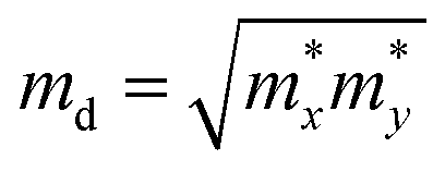
To quantify the carrier mobilities of the Janus TiXY monolayers, we adopted two models to calculate the effective masses, i.e. the parabolic band model and the DOS-averaged model.26,68–70 The subscripts “Par” and “DOS” are used to refer to the results of the two models, respectively. In the first model, the effective masses of electrons and holes in different directions can be computed according to the band dispersion at the extremum points according to the following formula:
 | (1) |
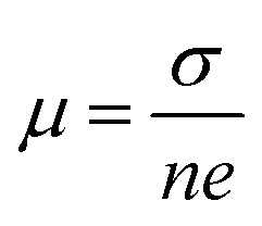 , where σ and n are conductivity and carrier concentration computed by the BoltzTrap code, respectively.
3. Results and discussion
3.1 Geometry and stability
The crystal structure and reciprocal space of the 2D Janus TiXY (X ≠ Y, X/Y = Cl, Br, I) with space group P3m1 (No. 156) are shown in Fig. 1, where each titanium (Ti) atomic layer is sandwiched between the X atomic layer and the Y atomic layer. For better calculations of carrier mobilities and piezoelectric coefficients, the rectangle cell is adopted. The hexagonal primitive cell and the rectangle cell are marked with black lines and red lines, respectively. Γ–M–K–Γ is used as a highly symmetric path in the first Brillouin zone of the primitive cell, while Γ–X–S–Y is used as a highly symmetric path of the rectangle supercell. The optimized lattice parameters a by PBE are 3.38 Å, 3.55 Å, and 3.62 Å for the hexagonal TiBrCl, TiClI, and TiBrI, respectively. The obtained bond lengths are also listed in Table 1 for our comparison. These results accord well with the previous reports.48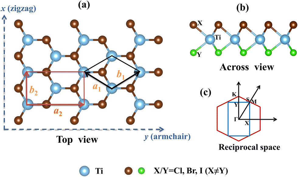 | ||
| Fig. 1 The optimized Janus structures and reciprocal space of the TiXY (X ≠ Y, X/Y = Cl, Br, I) monolayers. (a) Top view of the TiXY monolayers, the regions formed by the black and dark red wireframes represent the primitive cell and orthogonal cell of the Janus TiXY monolayers, respectively. (b) Side view of the TiXY monolayers. (c) The dark red regular hexagon illustrates the first Brillouin zone of the conventional cell with the high symmetry path Γ–M–K–Γ, and the dark blue rectangle exposits the first Brillouin zone of the orthonormal cell with the high symmetry path Γ–X–S–Y–Γ. | ||
The thermal dynamic stability of the optimized hexagonal Janus materials was investigated by AIMD simulations. As shown in Fig. S1 (ESI†), the average value of the total potential energy remained unchanged after 6 ps at 300 K and 600 K, and there were no broken bonds or structural reconstructions in the final crystal structures, indicating that the TiXY (X ≠ Y, X/Y = Cl, Br, I) monolayers are thermodynamically stable.
In Table 1, we listed the calculated elastic constants of the TiXY monolayers. It can be found that C11 > 0 and C11 > |C12|, which satisfies the Born criteria of mechanical stability,75 suggesting that the TiXY (X ≠ Y, X/Y = Cl, Br, I) monolayers are mechanically stable. According to the elastic theory,75 Young's modulus Y can be obtained. Our results indicate that the TiXY monolayers possess better mechanical flexibility when compared with graphene (344 N m−1)76 and monolayer MoSSe (113 N m−1).40 Notably, with the increase of atomic number of X/Y, the TiXY monolayers become more brittle. Furthermore, the phonon spectra are computed to verify the dynamic stabilities of the TiXY monolayers. Since there are three atoms in a unit cell, three acoustic branches and six optical branches can be found in the phonon spectra. As shown in Fig. 2, no negative values in the phonon frequency imply that the 2D Janus TiXY (X ≠ Y, X/Y = Cl, Br, I) monolayers can exist stably.
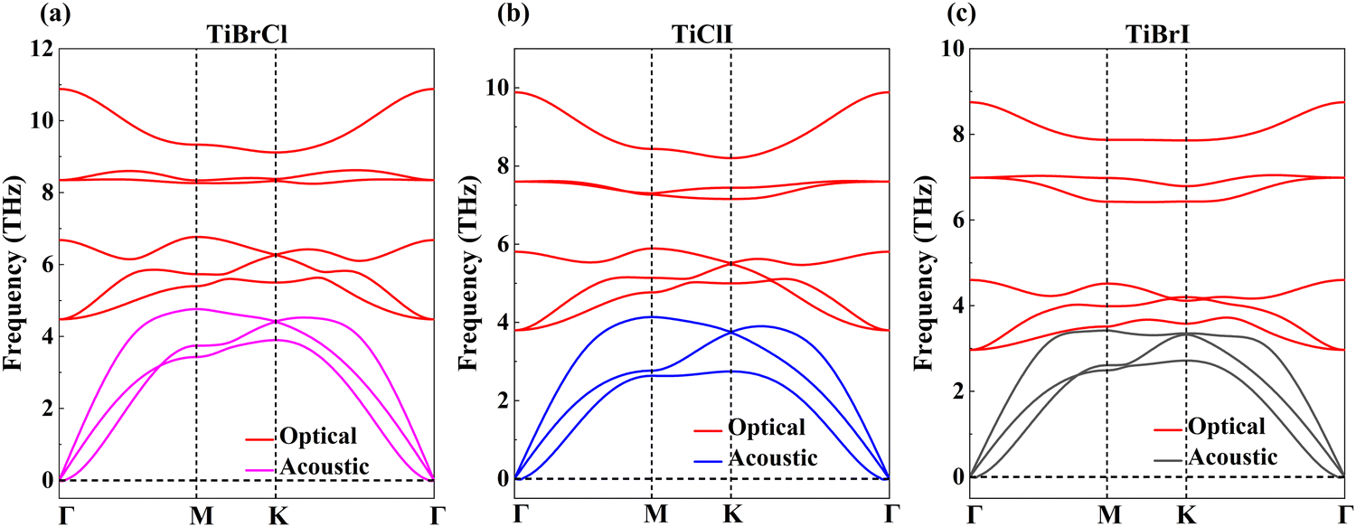 | ||
| Fig. 2 Phonon dispersion curves of the Janus TiXY monolayers: (a) TiBrCl, (b) TiClI, and (c) TiBrI, respectively. | ||
After testing the magnetism, it can be confirmed that the TiXY monolayers are non-magnetic materials, and their nonmagnetic phase is the most stable one, as shown in Fig. S2 (ESI†). To assess the synthesizability in the experiment of the Janus TiXY monolayers, the cohesive energy (Ecoh) was computed using the following expression,
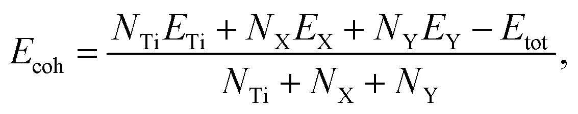 | (2) |
3.2 Electronic properties
Fig. 3 shows the projected band structures and partial density of states (PDOS) of the TiXY monolayers obtained by PBE. As shown in Fig. 3(a), (d) and (g), the bands near EF are mainly contributed by Ti-3d, and the bands of the Cl-3p orbitals are lower than those of the Br-4p and I-5p orbitals due to the stronger electronegativity. From Fig. 3(c), (f) and (i), it can be observed that the valence band maxima (VBMs) are mostly composed of the Ti-3dxy and Ti-3dx2−y2 orbitals, whereas the conduction band minimums (CBMs) mainly originated from the Ti-3dx2−y2 orbital. The corresponding PDOS of the X/Y-p and the Ti-3d are also displayed in Fig. 3(b), (e) and (h). It can be seen that the energies of the Ti-3dxy, dx2−y2 and dz2 orbitals are almost distributed around EF. Besides, the bands of X/Y-p at about −4 eV have a non-negligible component of Ti-3dxz and dyz, indicating that there may be a small overlap of X/Y-p and Ti-3dxz, dyz. The electronic band structures in the high-symmetry paths were calculated using PBE, PBE + SOC, HSE06, HSE06 + SOC, and G0W0 methods, as shown in Fig. S3 (ESI†). Table 2 shows the band gaps of the TiXY monolayers obtained by different methods. Since the bands near EF are mainly contributed by Ti-3d, the correction of SOC has little effect on the band gap. Besides, PBE underestimates the band gap due to that it cannot accurately describe the local Coulomb interaction between d electrons. For the result derived from the G0W0 method, as shown in Fig. S3(m)–(o) (ESI†), the bands of Ti-3d above (below) EF move upward (down), resulting in larger gaps (1.53, 1.32 and 1.22 eV for the TiBrCl, TiClI, and TiBrI monolayers, respectively). At the same time, these bands are obviously flatter than those of the other methods, indicating that the Ti-3d electrons calculated using the G0W0 method show more localization. Interestingly, no matter what method is used, the TiXY monolayers containing halogen atoms with larger atomic number have a smaller gap. | ||
Fig. 3 Calculated projected band structures (a, d and g), the conduction band minima, and the valence band maxima (c, f and i) in the TiXY (X ≠ Y, X/Y = Cl, Br, I) monolayers in the high-symmetry path obtained at the PBE level, where  and and  represent the points in the symmetric path of M–K and K–Γ, respectively. The width of the color range represents the spectral weight of the TiXY monolayers. The three pictures (b, e and h) in the middle area are the density of states of the sub-orbitals of the Ti-d and the total orbitals of X/Y-p. represent the points in the symmetric path of M–K and K–Γ, respectively. The width of the color range represents the spectral weight of the TiXY monolayers. The three pictures (b, e and h) in the middle area are the density of states of the sub-orbitals of the Ti-d and the total orbitals of X/Y-p. | ||
To get the bonding information, the electron localization function (ELF) of the TiXY monolayers in the (1 1 0) plane and Bader charge was analyzed. As shown in Fig. 4, the ELF values of Ti–X and Ti–Y bonds are both less than 0.5, indicating that monolayers TiXY are ionic compounds.80 Additionally, for the three compounds, the central Ti atom loses charge and the other two atoms gain charge. As the radius of the halogen atoms increases, the ability to acquire charge becomes weaker. For the TiBrCl and TiBrI monolayers, the difference in the number of obtaining charges of both X and Y are 0.09e, while the difference is as high as 0.16e in the TiClI monolayer. These results imply that the TiClI monolayer has a stronger internal electric field.
 | ||
| Fig. 4 The ELF of the TiXY (X ≠ Y, X/Y = Cl, Br, I) monolayers in the (1 1 0) plane, where the orange-yellow and blue regions represent the electron localization and delocalization, respectively. The gamut bars with values from 0.0 to 1.0 indicate the degree of delocalization of the electrons. The red wide arrow indicates the charge transfer. For the TiBrCl monolayer (a), the Ti atom transfers 0.64e to the Cl atom and 0.55e to the Br atom; for the TiClI monolayer (b), the Ti atom transfers 0.66e to the Cl atom and 0.50e to the I atom; for the TiBrI monolayer (c), the Ti atom transfers 0.60e to the Br atom and 0.51e to the I atom. | ||
3.3 Piezoelectric properties
Compared to other materials, Janus materials are more likely to produce larger piezoelectric effects due to the lack of reflection symmetry. Owing to the different abilities to obtain the charge of X and Y atoms, all three compounds generate polarized electric fields perpendicular to the 2D plane, and polarization in vertical directions along the low electronegativity atoms to the high electronegativity atoms. Furthermore, Fig. 5 shows the electrostatic potential Φ generated by the non-uniform charge distribution of the outermost atoms and the intrinsic electric fields of TiXY monolayers. Noticeably, the magnitude of the electrostatic potential gradient ΔΦ of the TiXY monolayers corresponds to the charge difference acquired by the outermost atoms. Furthermore, the intrinsic electric fields figured out by the slope of the planar average electrostatic potential between the outermost atoms are about 0.51, 2.46, and 2.72 eV Å−1 for TiBrCl, TiClI, and TiBrI monolayers, respectively. Both the out-of-plane dipole moment and the inherent electric field can polarize the interior of the TiXY monolayers, which results in piezoelectric properties. From the two aspects, TiClI and TiBrI have superior piezoelectric properties compared to TiBrCl.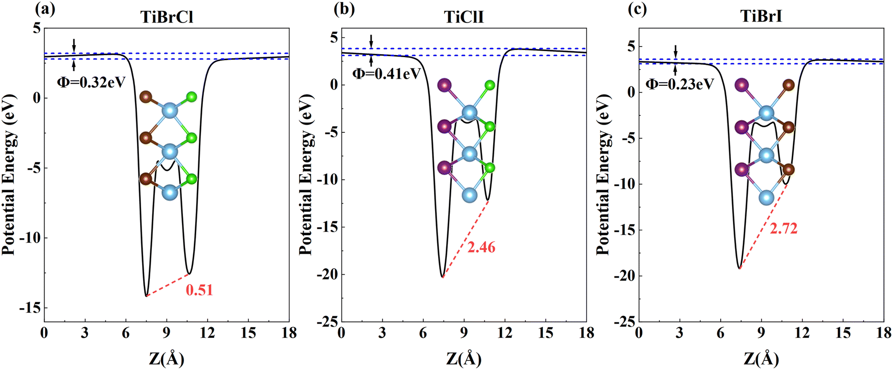 | ||
| Fig. 5 The plane average electrostatic potentials of TiXY monolayers: (a) TiBrCl, (b) TiClI, and (c) TiBrI, respectively. | ||
The piezoelectric tensor eik and piezoelectric coefficient dij in the 2D materials can be connected by this relationship in Voigt notation:62eik = dijCjk, where Cij denotes the elastic coefficient tensor. Considering the symmetry of the crystal, the number of independent tensor coefficients can be further reduced. Since the 2D Janus TiXY monolayers belong to the 3m point group symmetry, the piezoelectric tensor, piezoelectric coefficient, and the elastic coefficient tensor can be expressed as:
 | (3) |
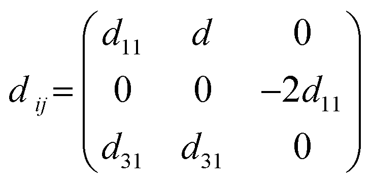 | (4) |
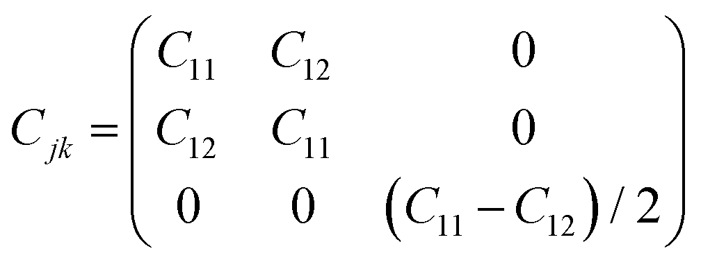 | (5) |
 | (6) |
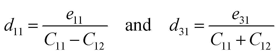
The obtained eik and dij of TiXY monolayers are summarized in Table 3. The in-plane piezoelectric coefficients d11 are 3.56, 4.41 and 4.58 pm V−1 for TiBrCl, TiClI, and TiBrI monolayers, respectively, which are comparable to or even better than those of many 2D piezoelectric materials, such as MoS2, MoSSe, MoSTe, WSSe, SnSSe, TiSO, and TiSeO.34,41,45,81 And, the out-of-plane piezoelectric coefficients d31 are 0.61, 1.63 and 1.05 pm V−1 for TiBrCl, TiClI, and TiBrI monolayers, respectively, which are superior to the ones like h-BN (0.13 pm V−1), Janus group-III materials (∼0.46 pm V−1), and HfSeTe (0.41 pm V−1).82–84 In particular, the TiClI monolayer has the largest out-of-plane piezoelectric coefficient d31 comparable to some new piezoelectric materials, Sb2Se2Te (1.57 pm V−1) and Sb2Te2Se (1.72 pm V−1) monolayers.85 Notably, there is an interesting phenomenon that the TiBrI monolayer possesses the largest in-plane piezoelectric coefficient, whereas the TiClI monolayer owns the greatest out-of-plane piezoelectric coefficient. The level of piezoelectric response is not only related to the polarization strength but also related to the mechanical properties of material structures. Softer materials with a lower Young's modulus in the same type of compounds are more sensitive to external stress. As shown in Table 1, Young's modulus of the TiClI monolayer is higher than that of the TiBrI monolayer, resulting in a lower in-plane piezoelectric coefficient d11 of TiClI though it has a slightly larger piezoelectric tensor e11 than TiBrI. Our results show that the Janus TiXY monolayers with large in-plane and out-of-plane piezoelectric coefficients may be promising candidate materials in the field of sensors and energy conversion.
| Material | e 11 (10−10 C m−1) | d 11 (pm V−1) | e 31 (10−10 C m−1) | d 31 (pm V−1) |
|---|---|---|---|---|
| TiBrCl | 2.30 | 3.65 | 0.57 | 0.61 |
| TiClI | 2.55 | 4.41 | 1.33 | 1.63 |
| TiBrI | 2.48 | 4.58 | 0.83 | 1.05 |
| MoS281 | 3.64 | 3.73 | — | — |
| MoSSe34 | 3.74 | 3.76 | 0.032 | 0.02 |
| MoSTe34 | 4.53 | 5.036 | 0.038 | 0.028 |
| WSSe34 | 2.57 | 2.26 | 0.018 | 0.011 |
| SnSSe41 | 1.009 | 2.251 | −0.091 | −0.114 |
| TiSO45 | 4.28 | 4.98 | — | — |
| TiSeO45 | 1.48 | 1.90 | — | — |
3.4 Optical properties
The optical properties of materials are key to measure the potential value of materials in the field of optoelectronics. Accordingly, we investigated the absorption amplitudes and range of the spectra of the TiXY monolayers using the complex dielectric function ε(ω), which can be written as: ε(ω) = ε1(ω) + iε2(ω), and the imaginary part ε2(ω) can be expressed as:67 | (7) |
It is known that the BSE results for the optical properties are in excellent agreement with the experiment,87–93 so we here adopted the G0W0 + BSE and HSE06 + SOC + RPA methods for comparison. The static dielectric function refers to the value of the dielectric function at zero energy, which can be used to characterize the strength of the optical properties of the materials. In Fig. 6, the dielectric constants in the TiBrCl, TiClI, and TiBrI monolayers are found to be 5.15, 5.99, and 6.42 using the HSE06 + SOC + RPA method, and 6.97, 8.14, and 8.48 using the G0W0 + RPA method. These data show an inverse proportionality with the computed band gaps, which follows Penn's rule:94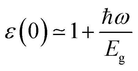 . Compared to the most promising materials in solar cells and optoelectronic applications,95,96 Janus TiXY monolayers with high dielectric constant are expected to be excellent optoelectronics. Because the BSE method includes the electron–electron (e–e) and electron–hole (e–h) interactions, the static dielectric constants using the BSE method are larger than those using the HSE06 + SOC + RPA method. For the same reason, the imaginary part ε2(ω) (see in Fig. 6) computed using the G0W0 + BSE method shows a red shift, and the first prominent peaks are located at 1.12, 1.06, and 1.04 eV for the TiBrCl, TiClI, and TiBrI monolayers, respectively. The significant peaks of the Janus TiXY monolayers are mainly in the infrared and visible light regions, implying that the TiXY monolayers have substantial potential to harvest solar energy efficiently.
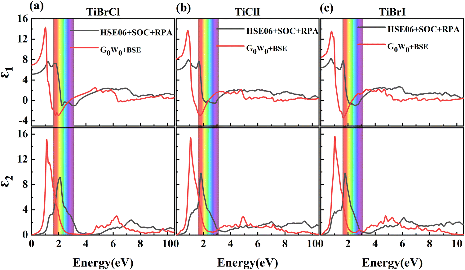 | ||
| Fig. 6 The real (top) and imaginary (bottom) parts of the dielectric function calculated using HSE06 + SOC + RPA and G0W0 + BSE methods for the Janus TiXY monolayers: (a) TiBrCl, (b) TiClI, and (c) TiBrI, respectively. | ||
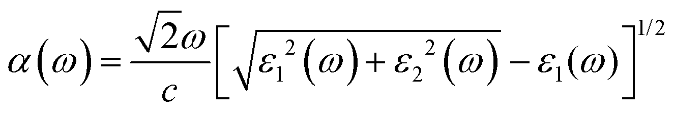
According to the dielectric function, the absorption coefficient α(ω) can be defined by:
 | (8) |
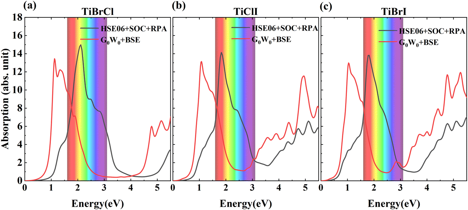 | ||
| Fig. 7 The absorption coefficients of TiXY monolayers calculated using HSE06 + SOC + RPA and G0W0 + BSE methods: (a) TiBrCl, (b) TiClI, and (c) TiBrI, respectively. | ||
3.5 Carrier mobility
Carrier mobility is one of the important conditions for determining whether a semiconductor is a good candidate for electronic and optoelectronic devices. We here use two models, i.e. the parabolic band model and the DOS-averaged model, to calculate the carrier mobility of the Janus TiXY monolayers.In the first model, we calculated the carrier mobilities according to the DP theory:72
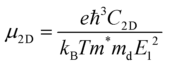 | (9) |
 . To acquire more accurate simulations, the Poisson effect was considered when the strain was applied. The main results are listed in Table 4, and more relevant information is shown in Fig. S4 and S5 (ESI†).
| Materials | Carrier types | C 2D (N m−1) |
|
E 1 (eV) | μ 2D (cm2 V−1 s−1) | |
|---|---|---|---|---|---|---|
| TiBrCl | Electrons | x | 78.426 | 1.149 | −2.714 | 119.227 |
| y | 78.463 | 2.387 | −3.610 | 32.453 | ||
| Holes | x | 78.426 | 0.643 | −4.278 | 200.26 | |
| y | 78.463 | 0.782 | −4.246 | 167.24 | ||
| TiClI | Electrons | x | 70.720 | 1.551 | −4.482 | 27.399 |
| y | 70.776 | 2.009 | −3.728 | 30.598 | ||
| Holes | x | 70.720 | 0.793 | −4.816 | 104.240 | |
| y | 70.776 | 0.779 | −4.568 | 118.040 | ||
| TiBrI | Electrons | x | 66.370 | 1.226 | −4.516 | 38.331 |
| y | 67.256 | 1.776 | −3.79 | 38.070 | ||
| Holes | x | 66.370 | 0.649 | −4.934 | 135.340 | |
| y | 67.256 | 0.674 | −4.516 | 157.630 |
As shown in Table 4, for the same carrier of the three monolayers, the electron effective masses  show strong anisotropy, while the hole effective masses
  represent slight anisotropy. Besides,
  are one order of magnitude smaller than
  under strain-free conditions. The smaller the effective mass, the faster the carrier responds to the promoting force of an external field. Hence, the hole mobilities μhPar are pretty higher than electron mobilities μePar. For the TiBrCl monolayer, μePar in the x-direction is about three times higher than that in the y-direction. In contrast, for the TiClI and TiBrI monolayers, μePar does not differ much in x- and y-directions. Moreover, the smaller deformation potential constant E1 and larger elastic constant C2D will also lead to considerable carrier mobility. For example, the TiBrCl monolayer with the greatest C2D and the smallest E1 has the largest μhPar, reaching about 200 cm2 V−1 s−1, though its
  is similar to those of the other two monolayers.
In the second model, we adopted the BTE approach to investigate the charge transport properties of the TiXY monolayers. Table 5 exhibits the effective masses and carrier mobilities of the TiXY monolayers, and Fig. S7 (ESI†) presents the Boltzmann transport results. In this model, the obtained  values (0.757, 0.911 and 0.728 me for the TiBrCl, TiClI, and TiBrI monolayers, respectively) are consistent with the results obtained from the parabolic band model. Our results show that the TiClI monolayer has the largest hole effective mass and the smallest hole mobility, and the hole effective masses and hole mobilities of the TiBrCl and TiBrI monolayers are relatively close. However, the
  values (3.106, 2.744 and 2.459 me for the TiBrCl, TiClI, and TiBrI monolayers, respectively) are pretty higher than those from the parabolic band model. The results of the DOS-averaged model indicated that the TiBrCl monolayer possesses the largest
  and the smallest μeDOS, in contrary to the conclusion of the parabolic band model (the TiClI monolayer has the smallest μePar). This difference is mainly due to that there are several minima whose energies are close to the CBM on the conduction band, resulting in underestimating
  in the parabolic band model. In all, the charge transport properties obtained using the BTE method using the DOS-averaged model are more reliable. Therefore, we have adopted the second model for further calculation of charge transport properties.
 and mobilities μDOS of the Janus TiXY monolayers using the DOS-averaged model. These data were calculated at the PBE + SOC level with a carrier density of 1011 cm−2 and the assumption of τ = 10 fs
| TiBrCl | TiClI | TiBrI | |
|---|---|---|---|
|
3.106 | 2.744 | 2.459 |
|
0.757 | 0.911 | 0.728 |
|
11.342 | 12.838 | 14.325 |
|
46.523 | 38.665 | 48.389 |
To investigate the influence of uniaxial strain on the charge transport properties, we calculated the carrier effective masses and mobilities of the Janus TiXY monolayers at different uniaxial compressive strains in the x-direction. Our results showed that the negative frequencies start to appear in the phonon spectra of the TiBrCl, TiClI, and TiBrI monolayers after the strain reaches −6%, −6%, and −4%, respectively. Therefore, it is reasonable to consider the strain within the range of −4% for the TiXY monolayers, as shown in Fig. S6 (ESI†). It can be seen from Fig. 8 and Table S1 (ESI†) that the  values of the TiXY monolayers generally increase with the increasing uniaxial compressive strain due to the difference of minima near the CBMs. The
  of the TiBrCl monolayer reaches the maximum at −3% strain (
 ), while those of both TiClI and TiBrI monolayers reach the maxima at −4% strain (
 for TiClI and TiBrI monolayers, respectively). Accordingly, the μeDOS values of the Janus TiXY monolayers generally decrease with the increasing strain and are smaller than those in the unstrained cases. Interestingly, the
  value of the TiBrI monolayer decreases sharply at −1% strain, which leads the μeDOS to reach a maximum of about 15 cm2 V−1 s−1, and the
  value decreases significantly with the increase of compression strain. This result may be due to that the VBMs composed of Ti-3dx2−y2 and Ti-3dxy become more dispersive with the increasing strain. At −4% strain, the
  reaches the minima of 0.668, 0.796, and 0.655 me for the TiBrCl, TiClI, and TiBrI monolayers, respectively. Simultaneously, the μhDOS reaches maxima, at about 53, 44, and 52 cm2 V−1 s−1, which are similar to the carrier mobilities of some other typical materials obtained from the same method, such as MoS2 (75 cm2 V−1 s−1),26 MoSO (20 cm2 V−1 s−1),26 and YTaON2 (50 cm2 V−1 s−1).70 Our calculations showed that the hole mobilities of the Janus TiXY monolayers can be enhanced under uniaxial strain, enabling them to be ideal p-type semiconductors.
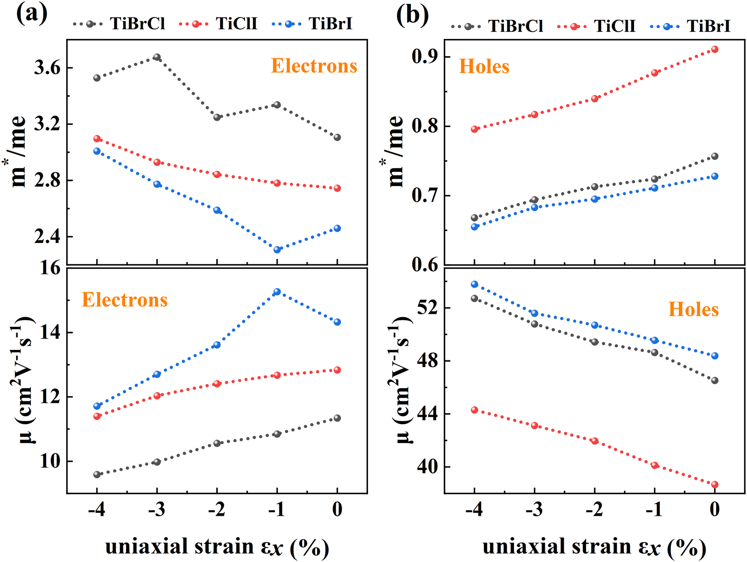 | ||
| Fig. 8 DOS-averaged carrier effective masses and mobilities under different uniaxial compressive strains for the Janus TiXY monolayers. | ||
4. Conclusions
Based on first-principles calculations, we have comprehensively studied the electronic structures, piezoelectric properties, optical properties, and carrier mobilities of novel TMH Janus TiXY (X ≠ Y, X/Y = Cl, Br, I) monolayers. First, we proved the thermal, dynamic, and mechanical stabilities for the TiXY monolayers from ab initio molecular dynamics, phonon spectra, and elastic constants, respectively. Using the PBE, PBE + SOC, HSE06 and HSE06 + SOC and G0W0 methods, it was determined that the TiXY monolayers are semiconductors with gaps of about 1 eV. The energy bands near the EF are mainly composed of the Ti-3d orbitals, particularly, the CBMs and VBMs mostly consist of the Ti-3dxy, and dx2−y2 orbitals. Additionally, all the three compounds have excellent in-plane and out-of-plane piezoelectric coefficients, suggesting their potential application in the piezoelectric sensors and energy conversion. In particular, the out-of-plane piezoelectric coefficient of the TiClI monolayer reaches 1.63 pm V−1. Using HSE06 + SOC + RPA and G0W0 + BSE methods, it was determined that all three monolayers exhibit large optical absorption in the visible and infrared regions, indicating that they may effectively convert solar energy. The relatively weak binding energies of the excitons indicate that the Janus TiXY monolayers can separate electrons and holes easily, which may be useful in the photocatalytic field. Ultimately, the carrier effective masses and mobilities in the TiXY monolayers were evaluated using the parabolic band model and the DOS-averaged model, and the second method is more accurate. In the DOS-averaged model, the TiBrI monolayer possesses the largest hole carrier mobility of about 48 cm2 V−1 s−1 under the unstrained case, which is close to the carrier mobilities of some other typical materials calculated using the same method. After applying uniaxial compressive strain, the electron mobilities of the TiXY monolayers are generally decreased with the increasing compressive strain, while the hole mobilities are increased due to the reduced hole effective masses. The characteristic that hole mobility is sensitive to strain indicates that the TiXY monolayers as p-type semiconductors have a promising future in the mechanical and electronic applications, such as mechanically controlled and compressive electronic devices.Author contributions
Qiu Yang: investigation, methodology, writing – original draft, and writing – review & editing. Tian Zhang: methodology, writing – original draft, and writing – review & editing. Cui-E. Hu: writing – review & editing, and supervision. Xiang-Rong Chen: visualization, supervision, and project administration. Hua-Yun Geng: project administration and software.Conflicts of interest
There are no conflicts of interest to declare.Acknowledgements
This work was supported by the National Natural Science Foundation of China (Grant No. 12074274, 12004269).References
- K. S. Novoselov, A. K. Geim, S. V. Morozov, D. Jiang, Y. Zhang, S. V. Dubonos, I. V. Grigorieva and A. A. Firsov, Science, 2004, 306, 666–669 CrossRef CAS.
- K. F. Mak, K. He, J. Shan and T. F. Heinz, Nat. Nanotechnol., 2012, 7, 494–498 CrossRef CAS PubMed.
- H. Yuan, X. Liu, F. Afshinmanesh, W. Li, G. Xu, J. Sun, B. Lian, A. G. Curto, G. Ye, Y. Hikita, Z. Shen, S. C. Zhang, X. Chen, M. Brongersma, H. Y. Hwang and Y. Cui, Nat. Nanotechnol., 2015, 10, 707–713 CrossRef CAS PubMed.
- S. Zhang, Z. Yan, Y. Li, Z. Chen and H. Zeng, Angew. Chem., Int. Ed., 2015, 54, 3112–3115 CrossRef CAS PubMed.
- L. Bastonero, G. Cicero, M. Palummo and M. Re Fiorentin, ACS Appl. Mater. Interfaces, 2021, 13, 43615–43621 CrossRef CAS.
- Z. Cui, S. Zhang, L. Wang and K. Yang, Micro Nanostruct., 2022, 167, 207260 CrossRef CAS.
- F. Y. Xu, Y. Zhou, T. Zhang, Z. Y. Zeng, X. R. Chen and H. Y. Geng, Phys. Chem. Chem. Phys., 2022, 24, 3770–3779 RSC.
- D. Deng, K. S. Novoselov, Q. Fu, N. Zheng, Z. Tian and X. Bao, Nat. Nanotechnol., 2016, 11, 218–230 CrossRef CAS PubMed.
- Q. Lu, Y. Yu, Q. Ma, B. Chen and H. Zhang, Adv. Mater., 2016, 28, 1917–1933 CrossRef CAS PubMed.
- K. Ren, H. Shu, W. Huo, Z. Cui and Y. Xu, Nanotechnology, 2022, 33, 345701 CrossRef.
- Y. Luo, C. Ren, Y. Xu, J. Yu, S. Wang and M. Sun, Sci. Rep., 2021, 11, 19008 CrossRef CAS PubMed.
- Z. Cui, H. Wu, K. Bai, X. Chen, E. Li, Y. Shen and M. Wang, Phys. E, 2022, 144, 115361 CrossRef CAS.
- J. Miao, S. Zhang, L. Cai, M. Scherr and C. Wang, ACS Nano, 2015, 9, 9236–9243 CrossRef CAS.
- B. Radisavljevic, A. Radenovic, J. Brivio, V. Giacometti and A. Kis, Nat. Nanotechnol., 2011, 6, 147–150 CrossRef CAS PubMed.
- E. Zhang, Y. Jin, X. Yuan, W. Wang, C. Zhang, L. Tang, S. Liu, P. Zhou, W. Hu and F. Xiu, Adv. Funct. Mater., 2015, 25, 4076–4082 CrossRef CAS.
- X. Liang, A. Garsuch and L. F. Nazar, Angew. Chem., Int. Ed., 2015, 54, 3907–3911 CrossRef CAS PubMed.
- Z. Ling, C. E. Ren, M. Q. Zhao, J. Yang, J. M. Giammarco, J. Qiu, M. W. Barsoum and Y. Gogotsi, Proc. Natl. Acad. Sci. U. S. A., 2014, 111, 16676–16681 CrossRef CAS PubMed.
- Y. Xiao, Y. Ding, H. Cheng and Z. Lu, Comput. Mater. Sci., 2019, 163, 267–277 CrossRef CAS.
- Y. Xie, M. Naguib, V. N. Mochalin, M. W. Barsoum, Y. Gogotsi, X. Yu, K. W. Nam, X. Q. Yang, A. I. Kolesnikov and P. R. Kent, J. Am. Chem. Soc., 2014, 136, 6385–6394 CrossRef CAS.
- Q. Xu, G. M. Yang and W. T. Zheng, Mater. Today Commun., 2020, 22, 100772 CrossRef CAS.
- M. Bernardi, M. Palummo and J. C. Grossman, Nano Lett., 2013, 13, 3664–3670 CrossRef CAS.
- H. R. Gutierrez, N. Perea-Lopez, A. L. Elias, A. Berkdemir, B. Wang, R. Lv, F. Lopez-Urias, V. H. Crespi, H. Terrones and M. Terrones, Nano Lett., 2013, 13, 3447–3454 CrossRef CAS PubMed.
- R. Roldán, J. A. Silva-Guillén, M. P. López-Sancho, F. Guinea, E. Cappelluti and P. Ordejón, Ann. Phys., 2014, 526, 347–357 CrossRef.
- W. Zhang, Z. Huang, W. Zhang and Y. Li, Nano Res., 2014, 7, 1731–1737 CrossRef CAS.
- M. Shahrokhi, P. Raybaud and T. Le Bahers, ACS Appl. Mater. Interfaces, 2021, 13, 36465–36474 CrossRef CAS PubMed.
- M. Shahrokhi, P. Raybaud and T. Le Bahers, J. Mater. Chem. C, 2020, 8, 9064–9074 CAS.
- A. Kuc and T. Heine, Chem. Soc. Rev., 2015, 44, 2603–2614 RSC.
- D. Xiao, G. B. Liu, W. Feng, X. Xu and W. Yao, Phys. Rev. Lett., 2012, 108, 196802 CrossRef PubMed.
- Z. Y. Zhu, Y. C. Cheng and U. Schwingenschlögl, Phys. Rev. B: Condens. Matter Mater. Phys., 2011, 84, 153402 CrossRef.
- K. F. Mak and J. Shan, Nat. Photonics, 2016, 10, 216–226 CrossRef CAS.
- A. Y. Lu, H. Zhu, J. Xiao, C. P. Chuu, Y. Han, M. H. Chiu, C. C. Cheng, C. W. Yang, K. H. Wei, Y. Yang, Y. Wang, D. Sokaras, D. Nordlund, P. Yang, D. A. Muller, M. Y. Chou, X. Zhang and L. J. Li, Nat. Nanotechnol., 2017, 12, 744–749 CrossRef CAS PubMed.
- J. Zhang, S. Jia, I. Kholmanov, L. Dong, D. Er, W. Chen, H. Guo, Z. Jin, V. B. Shenoy, L. Shi and J. Lou, ACS Nano, 2017, 11, 8192–8198 CrossRef CAS.
- Y. C. Cheng, Z. Y. Zhu, M. Tahir and U. Schwingenschlögl, EPL, 2013, 102, 57001 CrossRef.
- L. Dong, J. Lou and V. B. Shenoy, ACS Nano, 2017, 11, 8242–8248 CrossRef CAS PubMed.
- W.-J. Yin, B. Wen, G.-Z. Nie, X.-L. Wei and L.-M. Liu, J. Mater. Chem. C, 2018, 6, 1693–1700 RSC.
- F. Ersan and C. Ataca, Phys. Rev. Appl., 2020, 13, 064008 CrossRef CAS.
- L. Ju, M. Bie, X. Tang, J. Shang and L. Kou, ACS Appl. Mater. Interfaces, 2020, 12, 29335–29343 CAS.
- X. Ma, X. Wu, H. Wang and Y. Wang, J. Mater. Chem. A, 2018, 6, 2295–2301 RSC.
- S. Dimple, M. K. Mohanta, A. Rawat, N. Jena, R. Ahammed and A. De Sarkar, J. Phys.: Condens. Matter, 2020, 32, 315301 CrossRef PubMed.
- S. D. Guo, Phys. Chem. Chem. Phys., 2018, 20, 7236–7242 RSC.
- S. D. Guo, X. S. Guo, R. Y. Han and Y. Deng, Phys. Chem. Chem. Phys., 2019, 21, 24620–24628 RSC.
- S.-D. Guo, X.-S. Guo and Y. Deng, J. Appl. Phys., 2019, 126, 154301 CrossRef.
- S.-D. Guo, Y.-F. Li and X.-S. Guo, Comput. Mater. Sci., 2019, 161, 16–23 CrossRef CAS.
- W. Shi and Z. Wang, J. Phys.: Condens. Matter, 2018, 30, 215301 CrossRef PubMed.
- W. Chen, X. Hou, X. Shi and H. Pan, ACS Appl. Mater. Interfaces, 2018, 10, 35289–35295 CAS.
- A. Mogulkoc, Y. Mogulkoc, S. Jahangirov and E. Durgun, J. Phys. Chem. C, 2019, 123, 29922–29931 CAS.
- Z. Haman, M. Kibbou, I. Bouziani, Y. Benhouria, I. Essaoudi, A. Ainane and R. Ahuja, Phys. B, 2021, 604, 412621 CrossRef CAS.
- Y. Wang, W. Wei, H. Wang, N. Mao, F. Li, B. Huang and Y. Dai, J. Phys. Chem. Lett., 2019, 10, 7426–7432 CrossRef CAS.
- G. Kresse and J. Hafner, J. Phys.: Condens. Matter, 1994, 6, 8245–8257 CrossRef CAS.
- G. Kresse and J. Furthmuller, Phys. Rev. B: Condens. Matter Mater. Phys., 1996, 54, 11169–11186 CrossRef CAS PubMed.
- G. Kresse and J. Hafner, Phys. Rev. B: Condens. Matter Mater. Phys., 1993, 48, 13115–13118 CrossRef CAS PubMed.
- L. J. Sham and M. Schluter, Phys. Rev. B: Condens. Matter Mater. Phys., 1985, 32, 3883–3889 CrossRef CAS.
- G. Kresse and D. Joubert, Phys. Rev. B: Condens. Matter Mater. Phys., 1999, 59, 1758–1775 CAS.
- J. P. Perdew, K. Burke and M. Ernzerhof, Phys. Rev. Lett., 1996, 77, 3865–3868 CrossRef CAS PubMed.
- J. Paier, M. Marsman, K. Hummer, G. Kresse, I. C. Gerber and J. G. Angyan, J. Chem. Phys., 2006, 124, 154709 CrossRef CAS.
- R. W. Godby and R. J. Needs, Phys. Rev. Lett., 1989, 62, 1169–1172 CrossRef.
- A. Oschlies, R. W. Godby and R. J. Needs, Phys. Rev. B: Condens. Matter Mater. Phys., 1995, 51, 1527–1535 CrossRef PubMed.
- K. Kutorasinski, B. Wiendlocha, J. Tobola and S. Kaprzyk, Phys. Rev. B: Condens. Matter Mater. Phys., 2014, 89, 115205 CrossRef.
- S. Baroni, S. de Gironcoli, A. Dal Corso and P. Giannozzi, Rev. Mod. Phys., 2001, 73, 515–562 CrossRef CAS.
- A. Togo and I. Tanaka, Scr. Mater., 2015, 108, 1–5 CrossRef CAS.
- T. D. Kuhne, M. Iannuzzi, M. Del Ben, V. V. Rybkin, P. Seewald, F. Stein, T. Laino, R. Z. Khaliullin, O. Schutt, F. Schiffmann, D. Golze, J. Wilhelm, S. Chulkov, M. H. Bani-Hashemian, V. Weber, U. Borstnik, M. Taillefumier, A. S. Jakobovits, A. Lazzaro, H. Pabst, T. Muller, R. Schade, M. Guidon, S. Andermatt, N. Holmberg, G. K. Schenter, A. Hehn, A. Bussy, F. Belleflamme, G. Tabacchi, A. Gloss, M. Lass, I. Bethune, C. J. Mundy, C. Plessl, M. Watkins, J. VandeVondele, M. Krack and J. Hutter, J. Chem. Phys., 2020, 152, 194103 CrossRef PubMed.
- M. N. Blonsky, H. L. Zhuang, A. K. Singh and R. G. Hennig, ACS Nano, 2015, 9, 9885–9891 CrossRef CAS.
- M. Gajdoš, K. Hummer, G. Kresse, J. Furthmüller and F. Bechstedt, Phys. Rev. B: Condens. Matter Mater. Phys., 2006, 73, 045112 CrossRef.
- E. E. Salpeter and H. A. Bethe, Phys. Rev., 1951, 84, 1232–1242 CrossRef.
- G. Onida, L. Reining and A. Rubio, Rev. Mod. Phys., 2002, 74, 601–659 CrossRef CAS.
- S. Z. Karazhanov, P. Ravindran, A. Kjekshus, H. Fjellvåg and B. G. Svensson, Phys. Rev. B: Condens. Matter Mater. Phys., 2007, 75, 155104 CrossRef.
- J. S. Toll, Phys. Rev., 1956, 104, 1760–1770 CrossRef.
- G. Hautier, A. Miglio, D. Waroquiers, G.-M. Rignanese and X. Gonze, Chem. Mater., 2014, 26, 5447–5458 CrossRef CAS.
- G. Hautier, A. Miglio, G. Ceder, G. M. Rignanese and X. Gonze, Nat. Commun., 2013, 4, 2292 CrossRef PubMed.
- A. T. Garcia-Esparza, N. Tymińska, R. A. R. Al Orabi and T. Le Bahers, J. Mater. Chem. C, 2019, 7, 1612–1621 RSC.
- J. Bardeen and W. Shockley, Phys. Rev., 1950, 80, 72–80 CrossRef CAS.
- S. Bruzzone and G. Fiori, Appl. Phys. Lett., 2011, 99, 222108 CrossRef.
- G. K. H. Madsen and D. J. Singh, Comput. Phys. Commun., 2006, 175, 67–71 CrossRef CAS.
- S. P. Ong, W. D. Richards, A. Jain, G. Hautier, M. Kocher, S. Cholia, D. Gunter, V. L. Chevrier, K. A. Persson and G. Ceder, Comput. Mater. Sci., 2013, 68, 314–319 CrossRef CAS.
- R. C. Andrew, R. E. Mapasha, A. M. Ukpong and N. Chetty, Phys. Rev. B: Condens. Matter Mater. Phys., 2012, 85, 125428 CrossRef.
- E. Cadelano, P. L. Palla, S. Giordano and L. Colombo, Phys. Rev. B: Condens. Matter Mater. Phys., 2010, 82, 235414 CrossRef.
- J. Guan, Z. Zhu and D. Tomanek, Phys. Rev. Lett., 2014, 113, 046804 CrossRef CAS.
- R. Sant, M. Gay, A. Marty, S. Lisi, R. Harrabi, C. Vergnaud, M. T. Dau, X. Weng, J. Coraux, N. Gauthier, O. Renault, G. Renaud and M. Jamet, npj 2D Mater. Appl., 2020, 4, 08706 Search PubMed.
- W. Zhang, C. Chai and Y. Yang, J. Appl. Phys., 2022, 131, 224303 CrossRef CAS.
- K. Koumpouras and J. A. Larsson, J. Phys.: Condens. Matter, 2020, 32, 315502 CrossRef CAS.
- K.-A. N. Duerloo, M. T. Ong and E. J. Reed, J. Phys. Chem. Lett., 2012, 3, 2871–2876 CrossRef CAS.
- D. Dimple, N. Jena, A. Rawat, R. Ahammed, M. K. Mohanta and A. De Sarkar, J. Mater. Chem. A, 2018, 6, 24885–24898 RSC.
- Y. Guo, S. Zhou, Y. Bai and J. Zhao, Appl. Phys. Lett., 2017, 110, 163102 CrossRef.
- A. A. M. Noor, H. J. Kim and Y. H. Shin, Phys. Chem. Chem. Phys., 2014, 16, 6575–6582 RSC.
- J. Qiu, H. Li, X. Chen, B. Zhu, H. Guo, F. Zhang, Z. Ding, L. Lang, J. Yu and J. Bao, J. Appl. Phys., 2021, 129, 125109 CrossRef CAS.
- H. Shu, Y. Li, S. Wang and J. Wang, Phys. Chem. Chem. Phys., 2015, 17, 4542–4550 RSC.
- M. Shahrokhi, Appl. Surf. Sci., 2016, 390, 377–384 CrossRef CAS.
- M. Shahrokhi and C. Leonard, J. Alloys Compd., 2017, 693, 1185–1196 CrossRef CAS.
- M. Shahrokhi and C. Leonard, J. Alloys Compd., 2016, 682, 254–262 CrossRef CAS.
- H. Shu, Y. Wang and M. Sun, Phys. Chem. Chem. Phys., 2019, 21, 15760–15766 RSC.
- H. Shu, M. Zhao and M. Sun, ACS Appl. Nano Mater., 2019, 2, 6482–6491 CrossRef CAS.
- M. Re Fiorentin, F. Risplendi, M. Palummo and G. Cicero, ACS Appl. Nano Mater., 2021, 4, 1985–1993 CrossRef CAS.
- H. Shu, Appl. Surf. Sci., 2021, 559, 149956 CrossRef CAS.
- D. R. Penn, Phys. Rev., 1962, 128, 2093–2097 CrossRef CAS.
- M. Roknuzzaman, C. Zhang, K. K. Ostrikov, A. Du, H. Wang, L. Wang and T. Tesfamichael, Sci. Rep., 2019, 9, 718 CrossRef PubMed.
- M. Roknuzzaman, K. Ostrikov, K. Chandula Wasalathilake, C. Yan, H. Wang and T. Tesfamichael, Org. Electron., 2018, 59, 99–106 CrossRef CAS.
- P. Cudazzo, C. Attaccalite, I. V. Tokatly and A. Rubio, Phys. Rev. Lett., 2010, 104, 226804 CrossRef.
Footnote |
| † Electronic supplementary information (ESI) available. See DOI: https://doi.org/10.1039/d2cp03973g |
| This journal is © the Owner Societies 2023 |