The electronic structure and interfacial contact with metallic borophene of monolayer ScSX (X = I, Br, and Cl)†
Received
18th August 2022
, Accepted 13th October 2022
First published on 14th October 2022
Abstract
Two-dimensional (2D) semiconductors with excellent electronic and optical properties provide a great prospect for the fundamental research and application for the next-generation devices. Exploring the contact properties between 2D semiconductors and metal electrodes for improving the performance of nanodevices is of utmost importance. Motivated by the successful synthesis of bulk ScSI experimentally in a recent work [A. M. Ferrenti, M. A. Siegler, S. Gao, N. Ng and T. M. McQueen, Chem. Mater., 2022, 34, 12, 5443–5451], here we systematically investigate the intrinsic structural, electronic and optical properties of the novel monolayer ScSX (X = I, Br, and Cl) and their interfacial contact properties with the metal electrode of borophene using first-principles calculations. Interestingly, halogen X atoms with different electronegativities not only influence the intrinsic properties of monolayer ScSX, but also affect the interlayer coupling between monolayer ScSX and metallic borophene. The ScSI/borophene heterostructure forms a p-type Schottky contact, while both ScSBr/borophene and ScSCl/borophene heterostructures form a n-type Schottky contact. Moreover, our calculations demonstrate that strain engineering and applying an external electric field are effective strategies to regulate the Schottky barrier and contact types at the interface of ScSX/borophene. These findings provide a very promising path for designing tunable Schottky nanodevices with high-performance based on monolayer ScSX.
1 Introduction
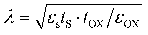
With the rapid development of the modern electronic information industry, integrated circuits tend to be miniaturized and highly integrated.1–4 The traditional size scaling can no longer meet the requirements of high-performance and low-power nanoelectronic devices.5–8 For instance, according to the equation  in the field of transistors, the length of the channel (λ) is proportional to the thickness (tS) of the semiconductor material.9,10 Therefore, two-dimensional (2D) ultra-thin semiconductors with prominent stability, suitable band gaps and high optical absorbance will be the hot products for the next-generation nanoelectronic technology.
Layered materials have triggered extensive interest because of their van der Waals type bonding.11–15 Advanced thin film growth technologies enable a variety of layered structures to be synthesized, such as transition metal dichalcogenides (TMDs), black phosphorene (BP), indium selenide (InSe), and Bi2O2Se.16–20 With the continuous emergence of various exfoliation methods, 2D forms of these layered structures have been successfully prepared. Compared with the bulk counterpart, 2D semiconductors show significant advantages, such as atomic-scale thickness, tunable band gaps, high mobility, and transparency.21–25 In particular, the interfacial contact between 2D semiconductors and metal electrodes is pivotal for further reducing the scale of electronic and optoelectronic devices.26,27 Relevant experimental and theoretical works show that the Fermi level pinning (FLP) effect at 2D semiconductor/2D metal interfaces is very weak, which means that the Schottky barrier and contact type can be easily modulated.28–31
Very recently, Ferrenti et al.32 successfully prepared a new exfoliatable semiconductor of bulk ScSI, which possesses an indirect band gap (∼2.0 eV) and exhibits remarkable optical performance. These characteristics provide an opportunity for ScSI to act as an optical element of the next-generation heterostructure devices. However, the electronic and photoelectric properties of its 2D forms are still unclear. The interfacial properties between 2D ScSI and metal electrodes in nanodevices have not been reported in the literature.
Herein, we comprehensively investigate the electronic structure and interfacial contact with metallic borophene of monolayer ScSX (X = I, Br, and Cl) based on first-principles calculations. By evaluating the exfoliation energy, lattice dynamics and thermal stability, it was found that monolayer ScSX is highly stable and can be prepared from its bulk crystal by mechanical exfoliation, similar to graphene. Monolayer ScSX exhibits a suitable band gap and significant anisotropic light absorption characteristics in the visible and ultraviolet regions. Moreover, the interfacial properties between monolayer ScSX and metallic borophene are explored. The ScSI/borophene heterostructure forms a p-type Schottky contact (ShC), while both ScSBr/borophene and ScSCl/borophene heterostructures form an n-type ShC. Further calculations show that that the Schottky barrier and contact type at the interface can be tuned by strain engineering and applying an external electric field. All these desirable properties make monolayer ScSX a powerful candidate material for future Schottky electronic/optoelectronic devices.
2 Computational details
Based on density functional theory (DFT), all first-principles calculations of the present work are carried out in the Vienna ab initio simulation package (VASP)33 adopting the plane-wave basis projector augmented wave (PAW) method.34 The Perdew–Burke–Ernzerhof (PBE) within generalized gradient approximation (GGA) is utilized to describe the exchange and correlation potential of electrons.35 Since the PBE functional does not describe the weak interactions very well, the empirical correction scheme of the DFT-D3 method proposed by Grimme36 is adopted for the van der Waals interactions. The hybrid function of Heyd-Scuseria-Ernzerhof (HSE06)37 is used to obtain a more accurate band structure for comparison. A large vacuum region of 30 Å is introduced along the Z direction to eliminate any interactions between the periodic images. An energy cut-off of 500 eV is applied for the geometry relaxation and electronic property calculations. The convergence tolerances for the energy and force on each atom do not exceed 10−5 eV and 0.01 eV Å−1, respectively. We use 11 × 8 × 1 and 4 × 8 × 1 k-point meshes for monolayer ScSX and ScSX/borophene heterostructures, respectively. Moreover, dipole correction is considered in the calculation of electronic properties. To ensure the dynamic stability of monolayer ScSX (X = I, Br, and Cl), Phonopy code38 is utilized to obtain the phonon dispersion curves through density functional perturbation theory (DFPT).39
3 Results and discussion
3.1 Structural, electronic and optical properties of monolayer ScSX (X = I, Br, and Cl)
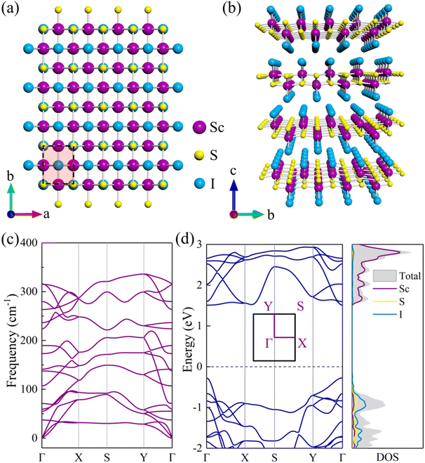
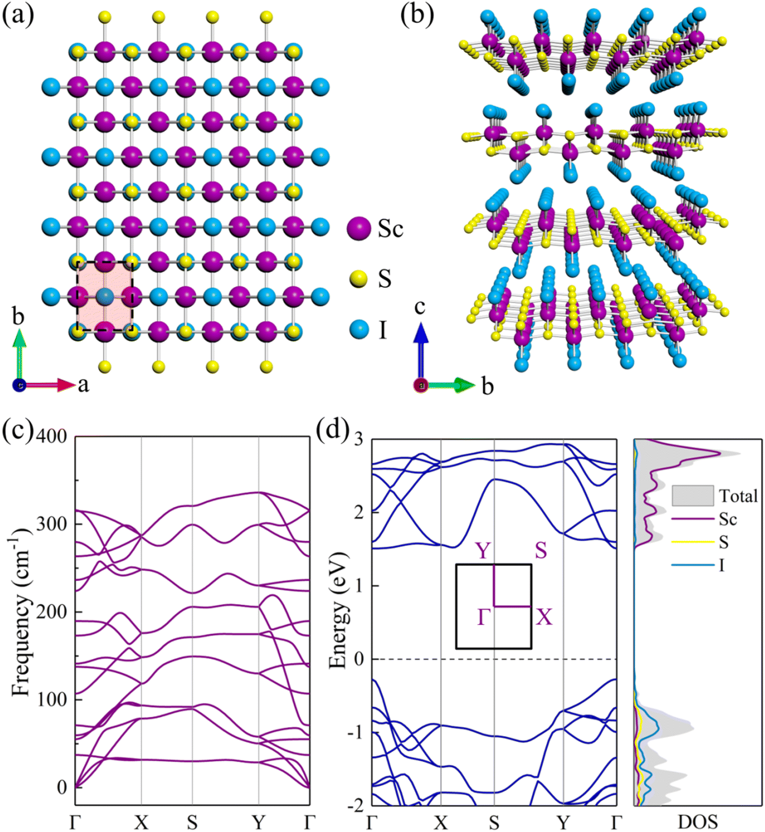
Bulk ScSI shows a layered orthorhombic structure with a space group of Pmmn (No. 59) as displayed in Fig. 1(a) and (b), and belongs to the FeOCl structure type. Based on DFT calculations, the optimized lattice parameters of ScSI are a = 3.90 Å, b = 5.06 Å, and c = 5.99 Å, very close to the experimental data (Table 1).32 Bulk ScSI has an indirect band gap of 1.65/2.63 eV obtained using the PBE/HSE06 functional, as depicted in Fig. S1 (ESI†). The valence band maximum (VBM) is at the Γ point, and the conduction band minimum (CBM) is located at the k-point between the X point and S point. Both PBE and HSE06 predict the same band dispersion characteristics of bulk ScSI. As is known, due to the unphysical self-Coulomb repulsion,35,40 the PBE functional usually underestimates the band gap. The HSE06 functional, which considers the short range exact Hartree–Fock exchange, can significantly reduce the Coulomb self-repulsion error.37,41 Compared with the experimental value (2.0 eV)32 of bulk ScSI, it is obvious that the PBE functional underestimates the band gap, while the HSE06 functional overestimates the band gap. The accurate band gap can be obtained by calculating the Green's function based on many-body perturbation theory such as the GW method.42 However, the GW approach is too expensive. Considering that the band gap calculated by the PBE functional is much closer to the experimental value, thus, the PBE functional is adopted for the following calculations.
 |
| | Fig. 1 (a) Top and (b) side views of bulk ScSI. (c) Phonon dispersion curve and (d) electronic band structure (left panel) and density of states (DOS, right panel) for monolayer ScSI. The high-symmetry points along the first Brillouin zone are Γ(0 0 0), X(0.5 0 0), S(0.5 0.5 0), Y(0 0.5 0), and Γ(0 0 0). The dashed line denotes the position of the Fermi level at 0 eV. | |
Table 1 The calculated lattice parameters a/b/c (Å), and electronic band gap Eg (eV) with PBE or the HSE06 functional for bulk ScSI and monolayer ScSX (X = I, Br, and Cl). D/I denotes that the band gap is direct or indirect
|
|
Bulk ScSI (this work) |
Bulk ScSI (exp)32 |
ML ScSI |
ML ScSBr |
ML ScSCl |
|
a
|
3.90 |
3.89 |
3.91 |
3.76 |
3.67 |
|
b
|
5.06 |
5.07 |
5.07 |
5.08 |
5.09 |
|
c
|
8.99 |
8.96 |
— |
— |
— |
|
E
g (PBE) |
1.65(I) |
2.0(I) |
1.78(D) |
2.12(D) |
2.08(I) |
|
E
g (HSE06) |
2.63(I) |
— |
— |
— |
— |
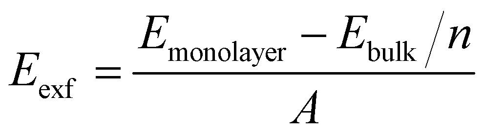
Generally, 2D crystals can be prepared by mechanical or liquid exfoliation from the layered van der Waals bonded crystals.43,44 Sequentially, the feasibility of monolayer ScSI exfoliated from its bulk crystal is investigated. The exfoliation energy (Eexf) of monolayer ScSI is calculated according to the following formula,45
| |  | (1) |
where
Emonolayer and
Ebulk represent the total energies of monolayer and bulk ScSI, respectively.
n denotes the number of layers, and
A represents the cross-sectional area of bulk ScSI. The calculated exfoliation energy of monolayer ScSI (0.22 J m
−2) is close to that of CrOCl (0.21 J m
−2)
46 successfully prepared experimentally,
47 which demonstrates the feasibility of experimental preparation. Furthermore, we calculate the phonon dispersion curve of monolayer ScSI to evaluate its dynamical stability. As shown in
Fig. 1(c), there are 18 branches in total, including 3 acoustical and 15 optical branches, which are contributed by 6 atoms in the unit cell. All frequencies in the whole Brillouin zone path (
Γ–
X–
S–
Y–
Γ) are positive, which confirms the dynamic stability of monolayer ScSI. The relaxed lattice parameters are
a = 3.91 Å and
b = 5.07 Å, very close to those of its bulk crystal. Intriguingly, unlike the bulk crystal, monolayer ScSI has a direct band gap (1.78 eV), and both the CBM and VBM are at the
Γ point (
Fig. 1(d)). We also calculate the density of states (DOS) near the Fermi level of monolayer ScSI as shown in the right panel of
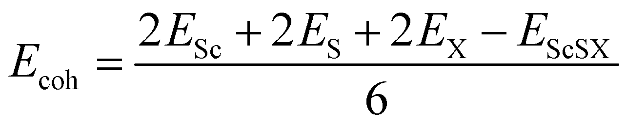
Fig. 1(d). This indicates that the VBM of monolayer ScSI is mostly contributed by I atoms, while the CBM is primarily determined by Sc atoms. Furthermore, we construct monolayer ScSBr and ScSCl by replacing the outermost I atoms with Br or Cl atoms. Cohesive energy (
Ecoh) represents the energy released by the individual free atoms when they form a compound.
48 It can be used to evaluate the thermal stability of compounds by the following formula,
| | 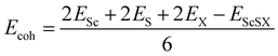 | (2) |
where
Esc,
ES,
EX and
EScSX represent the total energies of a single Sc atom, S atom, X atom and monolayer ScSX, respectively. The calculated cohesive energies of monolayer ScSI, ScSBr and ScSCl are 4.71, 4.92 and 5.12 eV per atom, respectively. As a comparison, the cohesive energies of graphene and BP are 5.69 and 3.69 eV per atom, respectively.
49 This result confirms a thermally stable structure of monolayer ScSX. Further phonon spectra and band structure show that monolayer ScSBr and ScSCl have good dynamic stability and semiconductor characteristics (Fig. S2, ESI
†). Among them, as the atomic radius of halogen X decreases from I to Cl, the lattice parameter
a gradually decreases, while
b gradually increases, and the band gap also gradually increases (
Table 1). The detailed information of the bond lengths and bond angles of monolayer ScSX is provided in Table S1 and Fig. S3 (ESI
†).
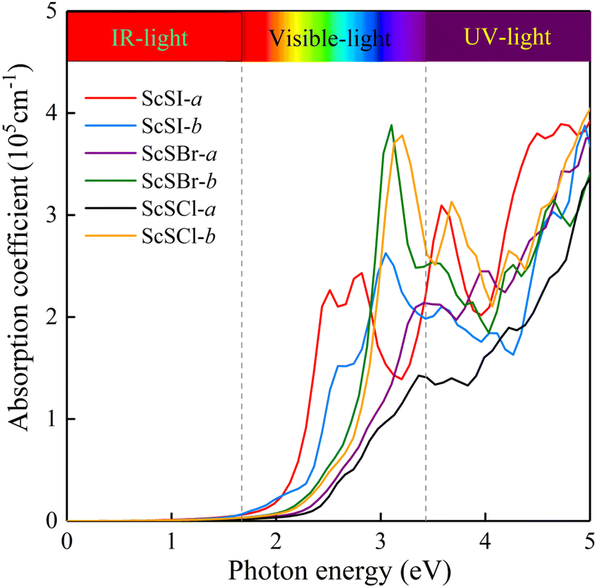
The absorption of sunlight is an important index to evaluate the application of 2D materials in optoelectronic devices.50–56 Herein, we calculate the optical absorption coefficient of monolayer ScSX by the following equation,
| | 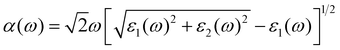 | (3) |
where
ε1(
ω) and
ε2(
ω) denote the real and imaginary parts of the dielectric function, respectively, which are related to the optical frequency (
ω). The absorption spectrum in
Fig. 2 exhibits an outstanding optical absorption coefficient (∼10
5 cm
−1) for monolayer ScSX in both visible- and ultraviolet-light regions. Obviously, monolayer ScSX exhibits in-plane anisotropic light absorption characteristics. In particular, in the visible-light region, the light absorption along the
b direction is significantly greater than that along the
a direction. This indicates that monolayer ScSX (X = I, Br, and Cl) are powerful candidate materials for application in optoelectronic devices.
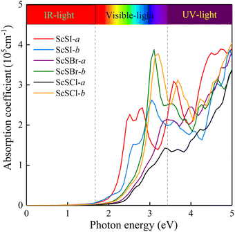 |
| | Fig. 2 Optical absorption coefficients of monolayer ScSX (X = I, Br, and Cl) as a function of photon energy. | |
3.2 Interfacial properties of ScSX (X = I, Br, and Cl)/borophene van der Waals heterostructures
In nanodevices, the electrical contact properties at the metal–semiconductor interface are as important as the intrinsic properties of the semiconductor. The contact resistance at the contact interface depends on the Schottky barrier.28–31 Here we chose honeycomb borophene as the metal electrode and construct a van der Waals heterostructure with monolayer ScSX to investigate its interfacial characteristics. The top and side views of the ScSI/borophene heterostructure are shown in Fig. 3(a) and (b). Before constructing the heterostructure, the structure of borophene with space group P6/mmm (No. 191) is optimized, and the fully relaxed lattice parameters are a = b = 2.92 Å, which is consistent with the previous work.57 Then the  supercell of borophene is strained to match the 3 × 1 supercell of monolayer ScSX, and the detailed lattice mismatch information is listed in Table S2 (ESI†).
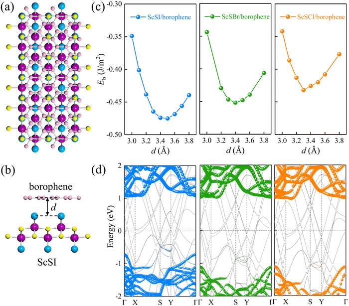 |
| | Fig. 3 (a) Top and (b) side views of the ScSI/borophene heterostructure. (c) The relationship between the binding energy and the interlayer spacing for ScSX (X = I, Br, and Cl)/borophene heterostructures. (d) Projected band structures of ScSX (X = I, Br, and Cl)/borophene heterostructures. The blue, olive green, and orange spheres denote the contributions from monolayer ScSI, ScSBr and ScSCl, respectively. The black dash line represents the Fermi level at 0 eV. | |
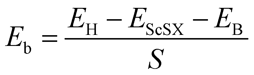
We define the equilibrium interlayer spacing (d) as the vertical distance from halogen X to borophene in the heterostructure (Fig. 3(b)). Before calculating the electronic properties, we test the binding energy (Eb) at different interlayer spacings,
| | 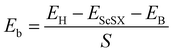 | (4) |
where
EH,
EScSX and
EB denote the total energies of the ScSX/borophene heterostructure, isolated monolayer ScSX and borophene, respectively.
S represents the interfacial contact area of the heterostructure supercell. The negative binding energy verifies the feasibility of experimental synthesis. As shown in
Fig. 3(c), the most stable interlayer spacings are 3.5, 3.4 and 3.3 Å for ScSI/borophene, ScSBr/borophene, and ScSCl/borophene heterostructures, respectively, which is a typical characteristic of weak van der Waals force. By comparing the binding energies in the equilibrium state in
Table 1, it is found that the interlayer coupling between ScSI and borophene is the strongest, while that of ScSCl/borophene is the weakest. The projected band structures of ScSX/borophene heterostructures are depicted in
Fig. 3(d). The van der Waals interactions help in maintaining the stability of ScSX/borophene heterostructures, thus well preserving the band structures of both ScSX and borophene, with almost no hybrid bands. In addition, the partial density of states (PDOS) of ScSX/borophene heterostructures is calculated (Fig. S4, ESI
†). The very tiny contribution of monolayer ScSX to the total DOS in the forbidden state zone also indicates that there is no interfacial gap state. The crystal orbital Hamilton population (COHP) analysis and electron location function (ELF) can well describe the bonding type.
58,59 We calculate the COHP between B atoms and halogen X atoms in three heterostructures, and the calculation results are shown in Fig. S5 (ESI
†). It can be seen that the antibonding state of three systems is very strong, especially in ScSCl/borophene, and the antibonding state almost completely offsets the bonding state, which indicates the weak interaction between B atoms and X atoms. This result is consistent with ELF analysis. As illustrated in Fig. S6 (ESI
†), the phenomenon that there is no electron density overlap between the ScSX layer and borophene layer further confirms that the interlayer coupling between ScSX and borophene depends on the weak van der Waals interaction. We can extract the Schottky barriers (
Table 2) of three contacts based on the Schottky–Mott rule,
60| | | ΦBn = ECBM − EF, ΦBp = EF − EVBM | (5) |
where
ΦBn and
ΦBp represent the Schottky barriers of electrons and holes, respectively. ScSI/borophene possesses a p-type ShC with an energy barrier of 0.72 eV, while both ScSBr/borophene and ScSCl/borophene show n-type ShC with energy barriers of 1.02 and 1.11 eV.
Table 2 Equilibrium interlayer spacing (d, Å), binding energy (Eb, J m−2), interface dipole (Dint, Debye), Schottky barrier (ΦBn and ΦBp, eV), and contact types for ScSX (X = I, Br, and Cl)/borophene heterostructures
| Heterostructures |
d
|
E
b
|
D
int
|
Φ
Bn
|
Φ
Bp
|
Contact types |
| ScSI/borophene |
3.5 |
−0.48 |
0.46 |
1.07 |
0.72 |
p-type ShC |
| ScBr/borophene |
3.4 |
−0.45 |
0.22 |
1.02 |
1.11 |
n-type ShC |
| ScCl/borophene |
3.3 |
−0.43 |
0.08 |
0.97 |
1.11 |
n-type ShC |
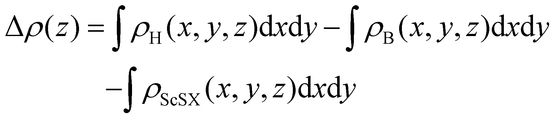
In order to further analyze the electronic properties of such 2D semiconductor/metal interface contact, the plane-average charge density difference along the Z-axis is calculated according to the following equation,
| | 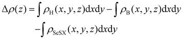 | (6) |
where
ρH(
x,
y,
z),
ρB(
x,
y,
z) and
ρScSX(
x,
y,
z) represent the charge densities of the ScSX/borophene heterostructure, isolated borophene and monolayer ScSX, respectively. As shown in
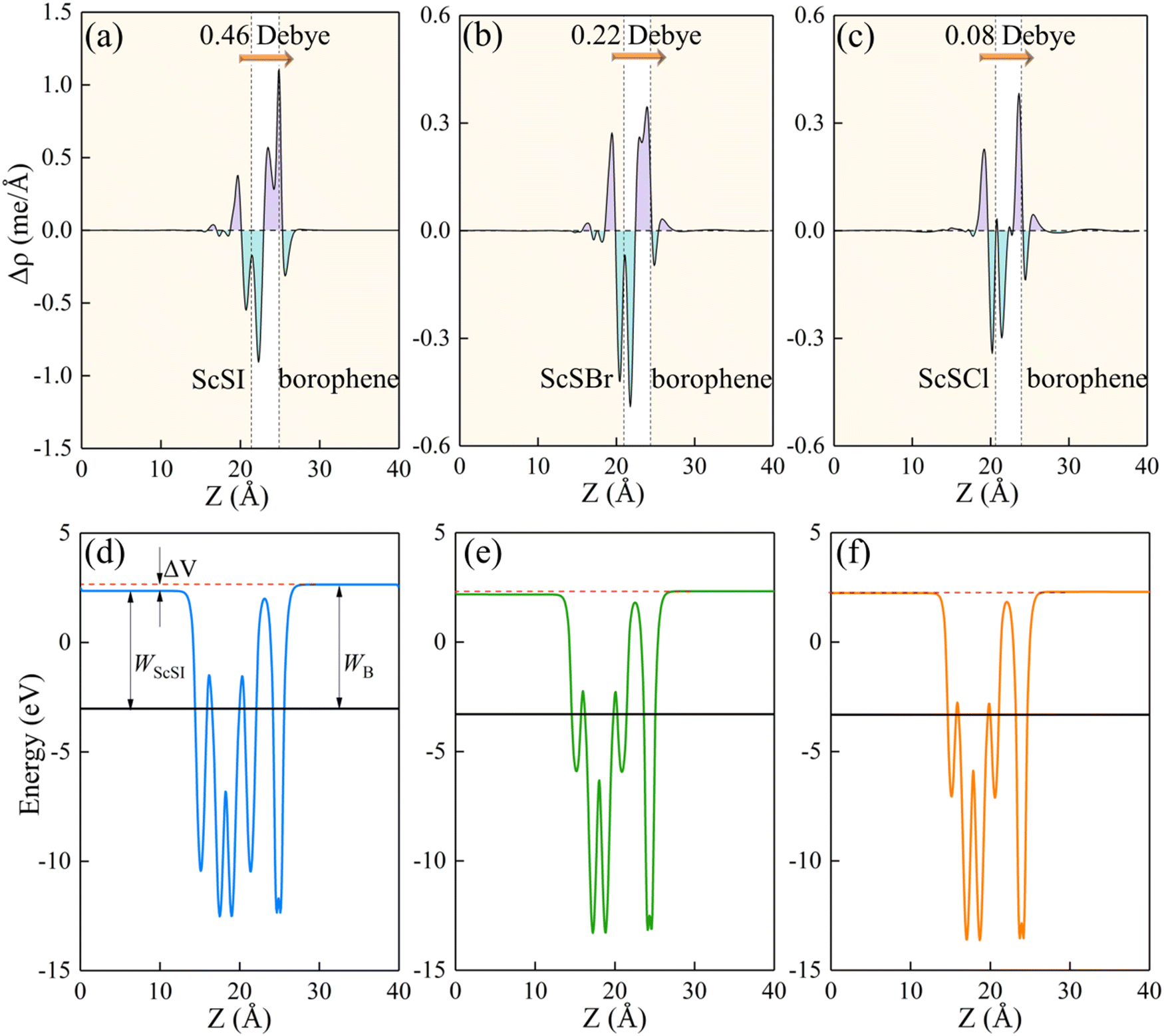
Fig. 4(a)–(c), charges are mainly depleted in the ScSX layer, while they are accumulated in the borophene layer, resulting in the charge transfer from the ScSX layer to the borophene layer. Among them, the interface charge transfer of the ScSI/borophene heterostructure is the largest owing to the strongest interlayer coupling. This is also consistent with the electronegativity order of halogen X,
i.e., I (2.66) < Br (2.96) < Cl (3.16). That is to say, I element has the smallest electronegativity and the weakest ability to bind electrons, thus, the charge transfer from monolayer ScSI to borophene is the largest.
 |
| | Fig. 4 The plane-average (a)–(c) charge density difference and (d) and (e) electrostatic profile of ScSX (X = I, Br, and Cl)/borophene heterostructures along the Z direction. The purple and cyan filled areas denote the charge accumulation and depletion, respectively. The interface dipole is indicated by the orange arrow. | |
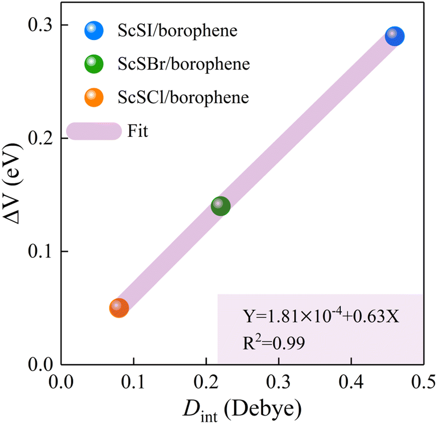
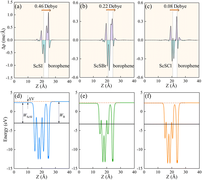
The redistribution of interface charges leads to the polarization of electron wave function, that is, the formation of interface dipoles.61 The interface dipoles of three heterostructures can be seen intuitively from Fig. 4(a)–(c), which is also the main factor affecting the band alignment.62 This influence of interface dipoles on contact properties can be reflected from the plane-average electrostatic profile as described in Fig. 4(e)–(f). After the contact of ScSX and borophene, there is a potential difference (ΔV) between the ScSX side and borophene side, that is ΔV = WB − WScSX, where WB and WScSX represent the work functions of borophene and ScSX in the heterostructure, respectively. The strongest interface dipole of ScSI/borophene also induced the most significant potential difference, which can also be considered as a built-in electric field. As shown in Fig. 5, the interface dipole and potential difference in these heterostructures show a positive linear correlation, which is also consistent with the Helmholtz equation.63
 |
| | Fig. 5 Linear function relationship between the interface potential difference (ΔV) and interface dipole (Dint) of ScSX (X = I, Br, and Cl)/borophene heterostructures. | |
3.3 Tunable electronic properties and Schottky barriers of ScSX (X = I, Br, and Cl)/borophene van der Waals heterostructures by strain and external electric field
As noted above, the charge transfer at the interface can affect the interlayer coupling. The tunable Schottky barrier and contact type are of great significance for improving the performance of nanodevices. Previous studies have shown that the strain and external electric field are very effective strategies to modulate the electronic properties of 2D semiconductors.64 Herein, we further study the effect of strain engineering on the interfacial properties by adjusting the interlayer spacings. As illustrated in Fig. 6(a) and (d), for the ScSI/borophene heterostructure, increasing the interlayer spacing can reduce the ΦBp, whereas decreasing the interlayer spacing can reduce the ΦBn. When the interlayer spacing is less than ∼3.3 Å, the transition from p-type to n-type ShC is achieved. ScSBr/borophene and ScSCl/borophene heterostructures also have the same trends when changing the interlayer spacings (Fig. S7 and S8, ESI†). The effect of strain on the interfacial properties of the ScSX/borophene heterostructure is closely related to the charge transfer and its associated interface dipole. As described in Fig. 6(b), with the increase of the interlayer spacing for the ScSI/borophene heterostructure, the interface dipole becomes smaller and smaller, and finally tends to 0 Debye. This can also be confirmed from the plane-average charge density difference in Fig. 6(c). As reported in the previous work,65,66 changing the interface dipole by varying the interlayer spacing is a very effective strategy to regulate the Schottky barriers. In the experiment, adjusting the interlayer spacing can be realized by a variety of methods, including the nanomechanical pressure, insertion of hexagonal border and nitride (h-BN) dielectric layer, and vacuum thermal annealing.67–69
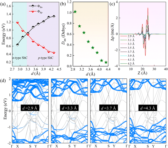 |
| | Fig. 6 (a) The change of ΦBn and ΦBp, (b) interface dipole, (c) plane-average charge density difference along the vertical direction, and (d) projected band structures for the ScSI/borophene heterostructure at various interlayer spacings. | |
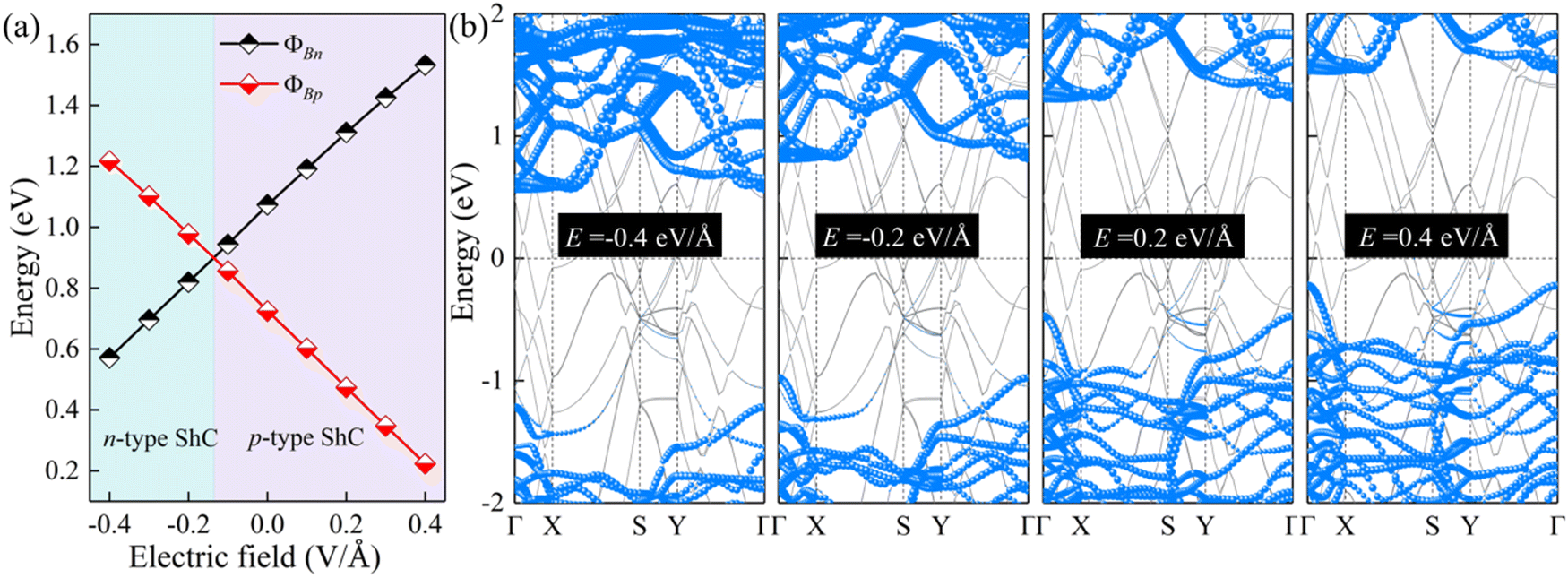
The interface dipole is equivalent to an internal electric field of the heterostructure, and thus applying an external electric field is also a way to change the dipole of the system. In view of this, the regulation effect should be similar to that of changing the interlayer spacings. Due to the typical layer characteristics, electrons are confined in the ultrathin structure of the 2D semiconductor, which can provide better electrostatic control.70,71 Herein, an external electric field (−0.4 to 0.4 V Å−1) is applied to ScSX/borophene heterostructures along the vertical direction, and the corresponding Schottky barriers are calculated. The positive direction of the external electric field is specified as ScSX pointing to borophene. The changes of the Schottky barriers and contact type for the ScSI/borophene heterostructure are shown in Fig. 7. The results verify our inference that increasing the positive electric field promotes the Fermi level to move downward and the corresponding ΦBp decreases. Conversely, the increased negative electric field accelerates the upward movement of the Fermi level, and the contact type changes to n-type ShC. This trend also occurs in ScSBr/borophene and ScSCl/borophene heterostructures under various external electric fields (Fig. S9 and S10, ESI†). The adjustable Schottky barrier and contact type of ScSX/borophene heterostructures make them promising candidates for future Schottky nanodevices, such as Schottky sensors, Schottky diodes, and photodetectors. This is because the tunability of the Schottky barrier leads to the change of interface resistance,28–31 which will make the nanodevice easier to capture the electrical signals with high sensitivity.72,73
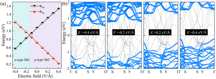 |
| | Fig. 7 (a) The change of ΦBn and ΦBp, and (b) projected band structures for the ScSI/borophene heterostructure under various external electric fields. | |
4 Conclusions
In summary, we first constructed monolayer ScSX (X = I, Br, and Cl) and systematically studied their structural, electronic and optical properties. All of these proposed materials exhibit high stability, suitable band gaps, and remarkable anisotropic light absorption characteristics. The interfacial contact properties of monolayer ScSX and metallic borophene are further investigated. Due to the electronegativity difference of halogen X atoms, the interlayer coupling strength of ScSX/borophene follows the order of I > Br > Cl. More interestingly, the ScSI/borophene heterostructure forms a p-type Schottky contact, while ScSBr/borophene and ScSCl/borophene heterostructures form an n-type Schottky contact. Taking the ScSI/borophene heterostructure as a prototype system, it is revealed that both strain engineering and applying an external electric field are effective strategies to tune the Schottky barrier and contact type at the interface. These findings provide valuable guidance for designing the tunable Schottky electronic and optoelectronic devices.
Author contributions
Keliang Wang: conceptualization, methodology, investigation, validation, formal analysis, data curation, and writing-original draft; Rengui Xiao: resources, supervision, the analysis with constructive discussions and funding acquisition; Tinghai Yang: formal analysis and methodology; Yong Zeng: visualization; Xiaoqing Tan: data curation and visualization.
Conflicts of interest
There are no conflicts to declare.
Acknowledgements
This work was supported by the National Natural Science Foundation of China (51764008).
References
- N. G. Orji, M. Badaroglu, B. M. Barnes, C. Beitia, B. D. Bunday, U. Celano, R. J. Kline, M. Neisser, Y. Obeng and A. E. Vladar, Nat. Electron., 2018, 1, 532–547 CrossRef PubMed.
- C. Liu, H. Chen, S. Wang, Q. Liu, Y. Jiang, D. W. Zhang, M. Liu and P. Zhou, Nat. Nanotechnol., 2020, 15, 545–557 CrossRef CAS PubMed.
- M. Zeng, Y. Xiao, J. Liu, K. Yang and L. Fu, Chem. Rev., 2018, 118, 6236–6296 CrossRef CAS PubMed.
- A. Razavieh, P. Zeitzoff and E. J. Nowak, IEEE Trans. Nanotechnol., 2019, 18, 999–1004 CAS.
- S. B. Desai, S. R. Madhvapathy, A. B. Sachid, J. P. Llinas, Q. Wang, G. H. Ahn, G. Pitner, M. J. Kim, J. Bokor, C. Hu, H. S. P. Wong and A. Javey, Science, 2016, 354, 99–102 CrossRef CAS PubMed.
- S. Zhang, H. Qu, J. Cao, Y. Wang, S. A. Yang, W. Zhou and H. Zeng, IEEE Trans. Electron Devices, 2022, 69, 857–862 CAS.
- H. N. Khan, D. A. Hounshell and E. R. H. Fuchs, Nat. Electron., 2018, 1, 14–21 CrossRef.
- S. Salahuddin, K. Ni and S. Datta, Nat. Electron., 2018, 1, 442–450 CrossRef.
- R. Yan, A. Ourmazd and K. F. Lee, IEEE Trans. Electron Devices, 1992, 39, 1704–1710 CrossRef CAS.
- W. Cao, J. Kang, W. Liu and K. Banerjee, IEEE Trans. Electron Devices, 2014, 61, 4282–4290 Search PubMed.
- D. L. Duong, S. J. Yun and Y. H. Lee, ACS Nano, 2017, 11, 11803–11830 CrossRef CAS PubMed.
- L. Du, T. Hasan, A. Castellanos-Gomez, G. Liu, Y. Yao, C. N. Lau and Z. Sun, Nat. Rev. Phys., 2021, 3, 193–206 CrossRef CAS.
- B. Liu, W. Xu, X. Long and J. Cao, Phys. Chem. Chem. Phys., 2022, 24, 18777–18782 RSC.
- M. A. Susner, M. Chyasnavichyus, M. A. McGuire, P. Ganesh and P. Maksymovych, Adv. Mater., 2017, 29, 1602852 CrossRef PubMed.
- A. Ambrosi and M. Pumera, Chem. Soc. Rev., 2018, 47, 7213–7224 RSC.
- A. AlMutairi, D. Yin and Y. Yoon, IEEE Electron Device Lett., 2018, 39, 151–154 CAS.
- P. Chang, X. Liu, F. Liu and G. Du, IEEE Electron Device Lett., 2019, 40, 333–336 CAS.
- L. Li, Y. Yu, G. J. Ye, Q. Ge, X. Ou, H. Wu, D. Feng, X. H. Chen and Y. Zhang, Nat. Nanotechnol., 2014, 9, 372–377 CrossRef CAS PubMed.
- R. Quhe, J. Liu, J. Wu, J. Yang, Y. Wang, Q. Li, T. Li, Y. Guo, J. Yang, H. Peng, M. Lei and J. Lu, Nanoscale, 2019, 11, 532–540 RSC.
- J. Yang, R. Quhe, Q. Li, S. Liu, L. Xu, Y. Pan, H. Zhang, X. Zhang, J. Li, J. Yan, B. Shi, H. Pang, L. Xu, Z. Zhang, J. Lu and J. Yang, Adv. Electron. Mater., 2019, 5, 1800720 CrossRef.
- S. Zeng, Z. Tang, C. Liu and P. Zhou, Nano Res., 2021, 14, 1752–1767 CrossRef.
- N. Lu, Z. Zhuo, H. Guo, P. Wu, W. Fa, X. Wu and X. C. Zeng, J. Phys. Chem. Lett., 2018, 9, 1728–1733 CrossRef CAS PubMed.
- S. Wang, C. Ren, H. Tian, J. Yu and M. Sun, Phys. Chem. Chem. Phys., 2018, 20, 13394–13399 RSC.
- L. Ju, J. Shang, X. Tang and L. Kou, J. Am. Chem. Soc., 2020, 142, 1492–1500 CrossRef CAS PubMed.
- H. Li, X. Jiang, X. Xu, G. Xu, D. Li, C. Li, B. Cui and D. Liu, Phys. Chem. Chem. Phys., 2021, 23, 2475–2482 RSC.
- D. S. Schulman, A. J. Arnold and S. Das, Chem. Soc. Rev., 2018, 47, 3037–3058 RSC.
- S. B. Mitta, M. S. Choi, A. Nipane, F. Ali, C. Kim, J. T. Teherani, J. Hone and W. J. Yoo, 2D Mater., 2021, 8, 012002 CrossRef CAS.
- J. Jeon, Y. Park, S. Choi, J. Lee, S. S. Lim, B. H. Lee, Y. J. Song, J. H. Cho, Y. H. Jang and S. Lee, ACS Nano, 2018, 12, 338–346 CrossRef CAS PubMed.
- S. Song, Y. Sim, S. Kim, J. H. Kim, I. Oh, W. Na, D. H. Lee, J. Wang, S. Yan, Y. Liu, J. Kwak, J. Chen, H. Cheong, J.-W. Yoo, Z. Lee and S. Kwon, Nat. Electron., 2020, 3, 207–215 CrossRef CAS.
- L. Cao, G. Zhou, Q. Wang, L. K. Ang and Y. S. Ang, Appl. Phys. Lett., 2021, 118, 013106 CrossRef CAS.
- W. X. Zhang, Y. Yin and C. He, Phys. Chem. Chem. Phys., 2020, 22, 26231–26240 RSC.
- A. M. Ferrenti, M. A. Siegler, S. Gao, N. Ng and T. M. McQueen, Chem. Mater., 2022, 34, 5443–5451 CrossRef CAS.
- G. Kresse and J. Furthmüller, Phys. Rev. B: Condens. Matter Mater. Phys., 1996, 54, 11169–11186 CrossRef CAS PubMed.
- G. Kresse and D. Joubert, Phys. Rev. B: Condens. Matter Mater. Phys., 1999, 59, 1758–1775 CrossRef CAS.
- J. P. Perdew, K. Burke and M. Ernzerhof, Phys. Rev. Lett., 1996, 77, 3865–3868 CrossRef CAS PubMed.
- S. Grimme, J. Comput. Chem., 2006, 27, 1787–1799 CrossRef CAS PubMed.
- J. Heyd, J. E. Peralta, G. E. Scuseria and R. L. Martin, J. Phys. Chem. Lett., 2005, 123, 174101 Search PubMed.
- A. Togo and I. Tanaka, Scr. Mater., 2015, 108, 1–5 CrossRef CAS.
- X. Gonze and C. Lee, Phys. Rev. B: Condens. Matter Mater. Phys., 1997, 55, 10355–10368 CrossRef CAS.
- J. M. Crowley, J. Tahir-Kheli and W. A. Goddard, J. Phys. Chem. Lett., 2016, 7, 1198–1203 CrossRef CAS PubMed.
- A. V. Krukau, O. A. Vydrov, A. F. Izmaylov and G. E. Scuseria, J. Chem. Phys., 2006, 125, 224106 CrossRef PubMed.
- M. Zhang, S. Ono, N. Nagatsuka and K. Ohno, Phys. Rev. B, 2016, 93, 155116 CrossRef.
- K. S. Novoselov, A. K. Geim, S. V. Morozov, D. Jiang, Y. Zhang, S. V. Dubonos, I. V. Grigorieva and A. A. Firsov, Science, 2004, 306, 666–669 CrossRef CAS PubMed.
- H. Liu, A. T. Neal, Z. Zhu, Z. Luo, X. Xu, D. Tománek and P. D. Ye, ACS Nano, 2014, 8, 4033–4041 CrossRef CAS PubMed.
- J. H. Jung, C. Park and J. Ihm, Nano Lett., 2018, 18, 2759–2765 CrossRef CAS PubMed.
- N. Miao, B. Xu, L. Zhu, J. Zhou and Z. Sun, J. Am. Chem. Soc., 2018, 140, 2417–2420 CrossRef CAS PubMed.
- T. Zhang, Y. Wang, H. Li, F. Zhong, J. Shi, M. Wu, Z. Sun, W. Shen, B. Wei, W. Hu, X. Liu, L. Huang, C. Hu, Z. Wang, C. Jiang, S. Yang, Q. Zhang and Z. Qu, ACS Nano, 2019, 13, 11353–11362 CrossRef CAS PubMed.
- Q. He, B. Yu, Z. Li and Y. Zhao, Energy Environ. Mater., 2019, 2, 264–279 CrossRef CAS.
- H. Qu, S. Guo, W. Zhou, B. Cai, S. Zhang, Y. Huang, Z. Li, X. Chen and H. Zeng, Nanoscale, 2019, 11, 20461–20466 RSC.
- S. Wang, H. Tian, C. Ren, J. Yu and M. Sun, Sci. Rep., 2018, 8, 12009 CrossRef PubMed.
- S. Wang, M. S. Ukhtary and R. Saito, Phys. Rev. Res., 2020, 2, 033340 CrossRef CAS.
- S. Wang, F. R. Pratama, M. S. Ukhtary and R. Saito, Phys. Rev. B, 2020, 101, 081414 CrossRef CAS.
- S. H. Xia, W. H. Fang, G. Cui and C. Daniel, Photochem. Photobiol. Sci., 2016, 15, 1138–1147 CrossRef CAS PubMed.
- S. Zhang, R. Pattacini, P. Braunstein, L. D. Cola, E. Plummer, M. Mauro, C. Gourlaouen and C. Daniel, Inorg. Chem., 2014, 53, 12739–12756 CrossRef CAS PubMed.
- P. Florindo, I. J. Marques, C. D. Nunes and A. C. Fernandes, J. Organomet. Chem., 2014, 760, 240–247 CrossRef CAS.
- S. Finck, J. T. Issenhuth, S. Despax, C. Sirlin, M. Pfeffer, C. Poidevin, C. Gourlaouen, A. Boeglin and C. Daniel, J. Organomet. Chem., 2014, 760, 248–259 CrossRef CAS.
- D. Geng, K. Yu, S. Yue, J. Cao, W. Li, D. Ma, C. Cui, M. Arita, S. Kumar, E. F. Schwier, K. Shimada, P. Cheng, L. Chen, K. Wu, Y. Yao and B. Feng, Phys. Rev. B, 2020, 101, 161407 CrossRef CAS.
- Y. Wu, C. He and W. Zhang, J. Am. Chem. Soc., 2022, 144, 9344–9353 CrossRef CAS PubMed.
- Y. Wu, C. He and W. Zhang, ACS Appl. Mater. Interfaces, 2021, 13, 47520–47529 CrossRef CAS PubMed.
- J. Bardeen, Phys. Rev., 1947, 71, 717–727 CrossRef.
- C. Gong, L. Colombo, R. M. Wallace and K. Cho, Nano Lett., 2014, 14, 1714–1720 CrossRef CAS PubMed.
- R. T. Tung, Phys. Rev. B: Condens. Matter Mater. Phys., 2001, 64, 205310 CrossRef.
- M. Bruening, R. Cohen, J. F. Guillemoles, T. Moav, J. Libman, A. Shanzer and D. Cahen, J. Am. Chem. Soc., 1997, 119, 5720–5728 CrossRef CAS.
- N. T. T. Binh, C. Q. Nguyen, T. V. Vu and C. V. Nguyen, J. Phys. Chem. Lett., 2021, 12, 3934–3940 CrossRef CAS PubMed.
- J. Li, W. Liu, W. Zhou, J. Yang, H. Qu, Y. Hu and S. Zhang, Phys. Rev. Appl., 2022, 17, 054009 CrossRef.
- J. Li, W. Zhou, L. Xu, J. Yang, H. Qu, T. Guo, B. Xu, S. Zhang and H. Zeng, Mater. Today Phys., 2022, 26, 100749 CrossRef CAS.
- M. Dienwiebel, G. S. Verhoeven, N. Pradeep, J. W. M. Frenken, J. A. Heimberg and H. W. Zandbergen, Phys. Rev. Lett., 2004, 92, 126101 CrossRef PubMed.
- X. Liu, A. Islam, J. Guo and P. X. L. Feng, ACS Nano, 2020, 14, 1457–1467 CrossRef CAS PubMed.
- S. Tongay, W. Fan, J. Kang, J. Park, U. Koldemir, J. Suh, D. S. Narang, K. Liu, J. Ji, J. Li, R. Sinclair and J. Wu, Nano Lett., 2014, 14, 3185–3190 CrossRef CAS PubMed.
- M. Chhowalla, D. Jena and H. Zhang, Nat. Rev. Mater., 2016, 1, 16052 CrossRef CAS.
- S. Rajput, M. X. Chen, Y. Liu, Y. Y. Li, M. Weinert and L. Li, Nat. Commun., 2013, 4, 2752 CrossRef CAS PubMed.
- Q. Pan, T. Li and D. Zhang, Sens. Actuators, B, 2021, 332, 129440 CrossRef CAS.
- Y. Guo, Y. Dong, X. Cai, L. Liu and Y. Jia, Phys. Chem. Chem. Phys., 2022, 24, 18331–18339 RSC.
|
| This journal is © the Owner Societies 2023 |
Click here to see how this site uses Cookies. View our privacy policy here. 
 ab,
Rengui
Xiao
ab,
Rengui
Xiao
 in the field of transistors, the length of the channel (λ) is proportional to the thickness (tS) of the semiconductor material.9,10 Therefore, two-dimensional (2D) ultra-thin semiconductors with prominent stability, suitable band gaps and high optical absorbance will be the hot products for the next-generation nanoelectronic technology.

 supercell of borophene is strained to match the 3 × 1 supercell of monolayer ScSX, and the detailed lattice mismatch information is listed in Table S2 (ESI†).