
 Open Access Article
 This Open Access Article is licensed under a
 Creative Commons Attribution 3.0 Unported Licence
Heteroepitaxial growth modes revisited
Jonas
Johansson
 *
*
Solid State Physics and NanoLund, Lund University, Box 118, 221 00 Lund, Sweden. E-mail: jonas.johansson@ftf.lth.se; Web: https://portal.research.lu.se/en/persons/jonas-johansson Tel: +46 46 2221472
First published on 28th September 2023
Abstract
It is well known that the outcome of a thin film deposition experiment on a foreign substrate is determined by surface and interface energetics, which can be collected in one parameter, the change in surface energy, Ω. It is common knowledge that at equilibrium conditions, Ω < 0 leads to two-dimensional (2D) growth and Ω > 0 leads to the formation of three-dimensional (3D) islands. Using classical nucleation theory, we demonstrate the existence of an interval for the chemical potential difference during growth, where 2D nucleation is favorable for sufficiently small, but positive Ω. For larger Ω, 2D nucleation is suppressed in favor of 3D nucleation. We exemplify this for two cases where epitaxial growth is performed at low supersaturation: vapor–liquid–solid growth of nanowires, and liquid phase epitaxy. First, we explain why certain axial nanowire heterostructures can be grown straight in both interface directions. Second, we explain the formation of multilayer heterostructures in liquid phase epitaxy. Finally, we discuss Stranski–Krastanov growth in a low supersaturation limit and show that there is a thermodynamically defined critical thickness, which increases with the chemical potential difference.
1. Introduction
The growth of thin films is a fundamental process in materials science and engineering and it is often used in various applications, such as electronic and optoelectronic devices, photovoltaic cells, and magnetic storage media. Thin film growth occurs through various mechanisms, including epitaxy, which is a term used to describe the growth of a film that is crystallographically oriented to the substrate (the starting material).1 Heteroepitaxy is the growth of a film of another material, and thus another crystallographic structure, than the substrate.2 Heteroepitaxy has revolutionized the semiconductor industry, allowing for the integration of materials with different properties into a single device, leading to improved performance and functionality.3 For example, heteroepitaxial growth of III–V semiconductors on silicon is very promising for high-performance, low-power, and cost-effective electronic devices, even if the growth is extremely challenging due to the dissimilarity of the materials.4 Another example of challenging heteroepitaxy is the emerging field of organic heterostructures.5There are three different growth modes for heteroepitaxy and these are the Frank–van der Merwe (FM), Volmer–Weber (VW), and Stranski–Krastanov (SK) growth modes,1,2 which are schematically illustrated in Fig. 1. The FM mode is a layer-by-layer growth mode in which the atoms of the growing film form complete monolayers on the substrate. This results in a two-dimensional (2D) film characterized by a smooth and uniform surface, as shown in Fig. 1a. The VW mode is a three-dimensional (3D) growth mode in which the atoms of the deposited material form islands on the substrate resulting in a rough surface, which is illustrated in Fig. 1b. The SK mode can be described as a combination of the FM and VW modes. Here, the film initially grows in a layer-by-layer fashion, but eventually switches to island growth as more material is deposited. The SK mode is characterized by 3D islands on a 2D wetting layer, as shown in Fig. 1c. These growth modes are well known and are usually described in textbooks on epitaxy and crystal growth.1,2,6–8 The FM and SK growth modes are widely applicable in semiconductor technology, for instance in the fabrication of quantum wells and quantum dots, respectively. Electronic and optoelectronic devices base on such structures as well as their preparation and properties are discussed in ref. 3 and references therein.
 | ||
| Fig. 1 Schematic illustration of the three heteroepitaxial growth modes: (a) Frank–van der Merwe (FM) 2D layer-by-layer growth, (b) Volmer–Weber (VW) 3D island growth, and (c) Stranski–Krastanov (SK) 2D wetting layer followed by 3D island growth. | ||
Bauer classified the three growth modes based on surface and interface energetics.9 For deposition of material A on material B, the change in surface energy is given by1
| Ω = γA + γi − γB, | (1) |
It is easy to show that if A wets B, then B does not wet A. Rewriting the inequality for A wetting B as γB − γA > γi and inserting this into γB + γi − γA results in γB + γi − γA > 2γi > 0, since γi > 0, which concludes the proof. In addition, if A does not wet B, no conclusions on B wetting A can be drawn. For this case, Ω > 0, which is equivalent to γB − γA < γi. Inserting this into γB + γi − γA results in γB + γi − γA < 2γi, implying that γB + γi − γA can be positive or negative.
Thus, from surface and interface energy conditions alone, it should not be possible to grow A on B and then B again. However, for some materials, such heterostructures are indeed possible and for others they seem virtually impossible to grow. In this investigation we will explain these differences using a nucleation theory approach. As we will consider nucleation in the capillarity approximation,10 our model is limited to growth at low to moderate supersaturation.
2. Theoretical model
Here we develop the model, which is based on classical nucleation theory. Nucleation is a process, constituting the initial step in the formation of a new phase or structure, such as the formation of solid crystals, crystalline layers, or crystallites from a nutrient phase, which often is a vapor or a liquid. During nucleation, a small number of atoms or molecules aggregate into a critical nucleus. When more atoms or molecules are added to this, it gets stable and growth commences. The driving force for nucleation and growth is the difference in chemical potential between the nutrient phase and the forming, solid phase. This chemical potential difference is a measure of the supersaturation, or the deviation from equilibrium. For small enough supersaturation, the critical nucleus is sufficiently large for macroscopic surface and interface energies to apply. This is known as the capillarity approximation, which is a central ingredient in classical nucleation theory. Excellent introductions to nucleation theory are given in the books by Kashchiev,11 Markov,6 and Dubrovskii.8On a flat surface, FM growth is initiated by 2D nucleation, and the free energy for 2D nucleation of A on B is given by
| F2D = −Δμi + αΩi + a2Di1/2, | (2) |
 | (3) |
 | (4) |
VW growth is initiated by 3D nucleation and the free energy for 3D nucleation of A on B is given by
| F3D = −Δμi + a3Di2/3, | (5) |
 | (6) |
 | (7) |
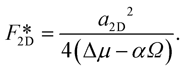
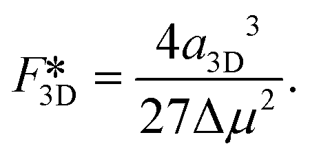
Next we compare the nucleation barriers for 2D and 3D nucleation in order to see at which conditions 2D nucleation is energetically favourable over 3D nucleation. Solving the inequality
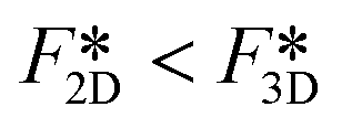 | (8) |
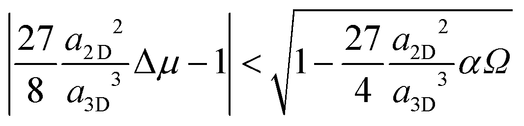 | (9) |
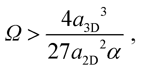 | (10) |
3. Results and discussion
Here we illustrate the theoretical model outlined in the previous section for a simple case, which captures the essential features of the model and we discuss this in terms of heterostructures in nanowires, multilayer heterostructures, and SK growth. We have chosen a geometry where the 2D nucleus is a circular disk and the 3D one is a hemisphere with isotropic surface energy, which is a common approximation in nucleation theory.12 In reality, the 3D nucleus is faceted, meaning that the model emulates a nucleus with an average surface energy of γN. For this geometry, the effective surface energies according to eqn (3) and (6) are given by and a3D = (3v/2)2/3π1/3(Ω − γA + 2γN), respectively. The interval of Δμ for FM growth is given by
 | (11) |
In Fig. 2 we illustrate the boundaries for 2D, 3D, and no nucleation with respect to the scaled coordinates Δμ/(αγA) and Ω/γA for the isotropic model γN = γA,v = γA. The upper branch of the 2D–3D boundary is given by the large Δμ branch of the solution to eqn (11) and the lower branch at positive Ω is given by the small Δμ branch of the solution to eqn (11), whereas the 2D-no nucleation boundary is given by Δμ = αΩ, since for Δμ > αΩ, 2D nucleation is possible, according to eqn (4). For Ω > 0, no nucleation is possible for Δμ < 0. For homoepitaxial conditions, Ω = 0, and the chemical potential difference for cross-over from 2D to 3D nucleation is given by Δμ0 = αγA/3 as can be seen in eqn (11). The maximum Ω for which 2D nucleation is possible, Ωm, can be calculated by setting the discriminant in eqn (11) to zero and solving the cubic equation. This equation has three real roots and the middle root is the physical one, resulting in Ωm ≈ 0.116γA. The corresponding chemical potential is Δμm ≈ 0.232αγA. In Fig. 2, we see that growth at equilibrium conditions results in 2D nucleation at Ω < 0 and 3D nucleation at Ω > 0. For growth at Δμ > 0, the Ω interval for 2D nucleation is widened and reaches into the positive Ω region. This interval increases for increasing Δμ until Δμm is reached where Ω = Ωm. Beyond this, the interval decreases until Δμ reaches Δμ0, where Ω = 0. For Δμ > Δμ0, 3D nucleation is energetically favourable independent of Ω. For Ω < 0, we note two interesting effects. First, 2D nucleation should indeed be possible at Δμ < 0, provided that the nucleation barrier according to eqn (4) is positive. Second, as Ω decreases, the chemical potential difference for cross-over from 2D to 3D nucleation also decreases. This can be intuitively understood in the following way: a negative Ω effectively increases Δμ for 2D nucleation making the nucleation barrier lower, as shown in eqn (4). This leads to a situation where 3D nucleation becomes energetically favourable at lower Δμ, according to eqn (8).
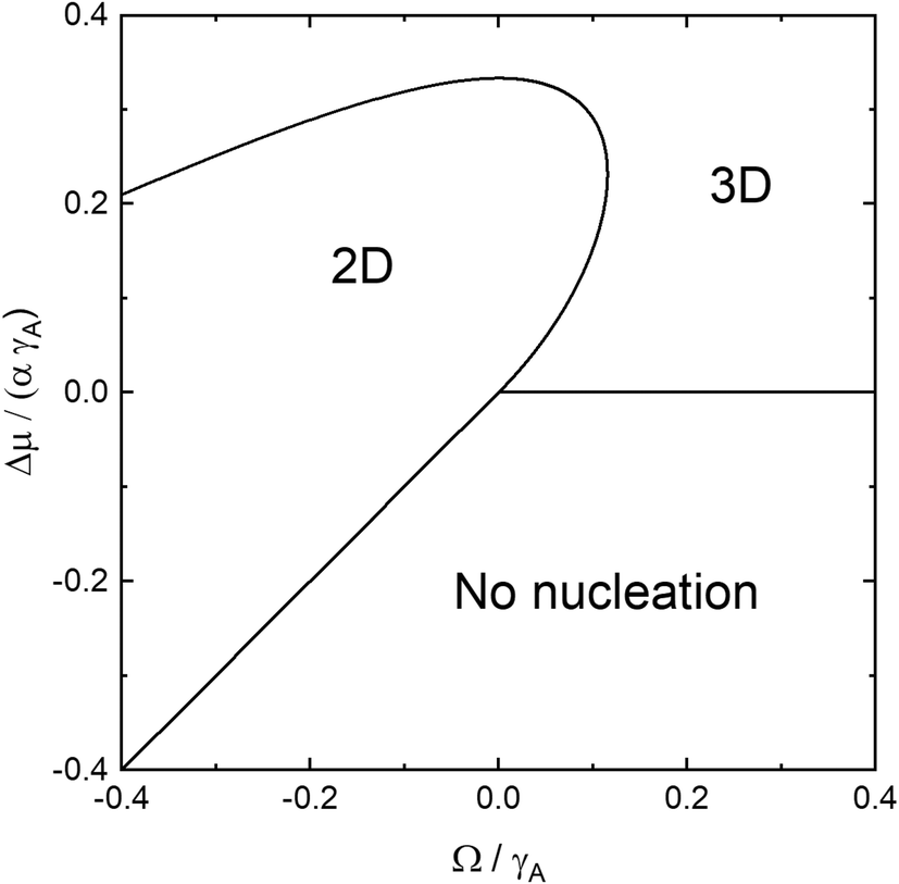 | ||
| Fig. 2 The boundaries for 2D, 3D, and no nucleation visualized using the scaled, dimensionless coordinates Δμ/(αγA) and Ω/γA for γN = γA,v = γA. | ||
In Fig. 3, we show the boundary for 2D–3D nucleation for positive Ω, using the same coordinates as in Fig. 2 and γA,v = γA but for different values of the surface energy of the 3D nucleus, γN, which also in this case is approximated as a hemisphere. Here we see that the region for 2D nucleation for Ω > 0 increases as the surface energy of the 3D nucleus increases. This is not surprising, since a large value of γN/γA makes 3D nucleation harder and thus favors 2D nucleation.
 | ||
| Fig. 3 The boundaries for 2D–3D nucleation for four different values of the surface energy of the 3D nucleus, γN, visualized using the same scaled coordinates as in Fig. 2. The dashed line represents the small Δμ asymptote of the 2D–3D boundary, which is independent of γN. | ||
Let us now discuss some practical implications of our model. Since our model is based on classical nucleation theory in the capillarity approximation, it is valid for growth at low supersaturation. Two relevant examples are growth of semiconductor nanowires by the vapor–liquid–solid (VLS) mechanism8 and planar growth by liquid phase epitaxy (LPE).2
In VLS growth, metal particles, most often gold, are used to seed and guide the growth of semiconductor materials. The metal particles are placed on a semiconductor surface and reactant gases dissolve, at elevated temperature, into the liquid metal. The metal becomes supersaturated and semiconductor nanowires grow, layer by layer, at the interface between the metal and the semiconductor. Each new layer is initiated by a nucleation event and the growth process is well described by monocentre classical nucleation.13,14 As an example, for growth of Au catalysed GaAs nanowires at T = 450 °C and with Ga and As molar fractions of cGa = 30% and cAs = 0.01–0.1%, close to what is reported in ref. 15, we can estimate the chemical potential difference to be Δμ = 0.42 × 10⁻²⁰–2.7 × 10⁻²⁰ J with the thermodynamic data from ref. 16. Using a surface energy value for the interface Au–GaAs of γA = 0.5 J m−2,8 and letting h be a monolayer step in the {111} direction for GaAs, we get Δμ0 = 2.3 × 10⁻²⁰ J, indicating that homoepitaxial growth of gold catalysed GaAs nanowires proceeds in a layer-by-layer fashion, except for the highest As concentration at which 3D nucleation is favourable. Here we note that vapor–solid growth in MOVPE and MBE operates at around Δμ ≈ 50 × 10−20 J,2 which is at least an order of magnitude higher than for VLS growth. Moreover, the capillarity approximation breaks down at Δμ ≈ 11 × 10−20 J, where the critical nucleus consists of one Ga–As pair (calculated for a 2D circular nucleus with γA = 0.5 J m−2).
An especially interesting feature of nanowires is the possibility to fabricate axial heterostructures, where the material is changed during growth. In their thorough investigation, Dick et al.17 experimentally studied nanowire heterostructure formation for a large number of material combinations. In most cases it was found that if straight nanowires were formed when material A was grown on material B, then the attempt to grow material B on A failed and resulted in kinked nanowires. The authors interpreted their results in terms of FM and VW growth so that straight growth was associated with FM growth whereas kinked growth was a result of VW growth at the heterointerface. In two material combinations, straight growth could be achieved in both interface directions, that is for A on B and B on A. These combinations are GaAs–GaP and InAs–InP. For these materials, the interface energies between the semiconductor and the gold alloy catalyst are likely to be similar, as discussed by Dick et al.,17 so that γA − γB is small and Ω ≈ γi. According to our model, straight growth will occur if Δμ can be selected so that the growth proceeds by 2D nucleation. We can demonstrate here that even for material combinations with small γA − γB, this can be more or less difficult and success is not guaranteed. Let γA − γB = δγi, with δ ≥ 0, and let ΩAB = γA + γi − γB, that is, the definition of Ω according to eqn (1), which we have used in Fig. 2 and 3. Let ΩBA = γB + γi − γA, which is the Ω for deposition of B on A. Now we see that ΩAB = (1 + δ)γi and ΩBA = (1 − δ)γi. If δ < 1, both ΩAB and ΩBA are positive, and at equilibrium conditions wetting is unfavourable in both directions. If ΩAB is smaller than the 2D–3D cross-over Ω at the growth Δμ, then it is possible to grow straight A-on-B nanowires and consequently also straight B-on-A nanowires, since ΩBA < ΩAB. In the extremes, we require that ΩAB < Ωm for straight growth in both interface directions. That is, γi < (x − 1)γA + γB, where x depends on the ratio γN/γA (for γN/γA = 1, x ≈ 0.116, see Fig. 3). So for γN/γA = 1 and γA = γB = 0.5 J m−2, γi < 0.058 J m−2 for straight growth to be possible. This seems to be a very small value and in general these interface energies are unknown. We are only aware of the value of one such interface energy, the one for AlAs–GaAs, which has been estimated to 0.05 J m−2 for the (001) oriented interface using a semiempirical potential energy approach.18 Considering the similarity of the material systems, it is not unreasonable that γi for GaAs–GaP and InAs–InP have such small values. The InAs–InP material system was reported to be more difficult than the GaAs–GaP one,17 since the morphology of InAs on InP (straight or kinked) was found to depend on growth conditions. A plausible explanation is that γi could be slightly larger for this material system as compared to GaAs–GaP, leading to a smaller Δμ interval for 2D nucleation and thus higher sensitivity to growth conditions.
Dick et al.17 did not report any observation of kinked growth in either interface direction, which would require quite special conditions: a very small difference, γA − γB, a significant γi, and growth close to equilibrium or at very high supersaturation so that 3D nucleation is always favoured. Finally, we note that the cross-over from 2D to 3D nucleation at Δμ > Δμ0 for Ω = 0 can explain kinking in homoepitaxial nanowires.
Now we turn to our next example, LPE growth. LPE and VLS growth are similar in that the nutrient phase is a metallic melt2 and thus the chemical potential differences during growth are similar. However, in LPE the melt is supplied from a chamber directly in contact with the substrate and the melt covers the entire sample. If heterostructures are desired, the sample can be moved from one chamber to another, containing a different melt. In LPE, multi-layered heterostructures in the material system AlAs–GaAs have been reported.19–21 As previously noted, at equilibrium conditions, growth of AlAs on GaAs and GaAs on AlAs cannot both proceed in a 2D layer-by-layer fashion. According to our previous discussions, if one material wets the other, then wetting is prohibited in the other interface direction. The explanation is similar to the previous explanation for nanowire heterostructures. That is, if the two melt-semiconductor interface energies are similar and the interface energy between GaAs and AlAs is sufficiently small (in this particular case we have already seen that it is 0.05 J m−2)18 then there is a Δμ interval, where 2D growth is also possible for the less favourable interface direction.
Our model can also be used to gain some new insights into SK growth at low supersaturation. In this growth mode the first molecular layer or layers completely wets the substrate surface while continued growth leads to the formation of 3D islands. SK growth can occur in heteroepitaxial materials combinations with a few percent lattice mismatch strain. In LPE, SK growth has been observed in a few material systems, such as GeSi on Si,22 InSb on InAs,23 and GaInAs on GaAs.24 This growth mode can be understood in such a way that the effective interface energy increases with the number of layers as an effect of strain energy accumulation during the growth of the 2D wetting layer. At a certain critical wetting layer thickness, Ω surpasses the 2D–3D boundary and 3D islands form on top of the wetting layer. As can be seen in Fig. 3, when Δμ increases from zero, the 2D–3D cross-over Ω, and thus the critical thickness, also increases. It is known that the onset of island formation sets in at a thicker wetting layer when depositing at a higher supersaturation.25 The explanation relies on the kinetics of island formation, implying that by a high deposition rate, the thermodynamically defined critical thickness can be surpassed.26,27 As we have seen, the thermodynamically defined critical thickness also increases with increasing Δμ from its equilibrium value at Δμ = 0.
We can explicitly illustrate this by letting the interface energy depend on the strain energy in the wetting layer28 and express Ω as
| Ω = γA − γB + γ0i + Cε2hΘ, | (12) |
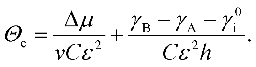 | (13) |
As a final note, we comment on growth at high supersaturation. It is well known that multilayer heterostructures and SK islands can be grown in MOVPE and MBE,3 which operate at supersaturations where the capillary approximation cannot be expected to be valid, as previously discussed. Such cases are best handled by atomistic approaches to nucleation, including rate equations, Monte Carlo techniques, and molecular dynamics simulations. From such an investigation we would expect qualitatively similar results, namely that a high enough deposition rate will enable heterostructure growth of planar layers in either interface direction for certain materials. For SK growth we would expect a kinetically defined critical thickness, increasing with the deposition rate.25–27 An atomistic treatment is, however, clearly beyond the scope of the current investigation and left for future work.
4. Conclusions
We have developed a model to deepen the understanding of heteroepitaxial growth modes for nucleation limited growth. Since we use classical nucleation theory in the capillarity approximation, our model is valid for growth at low supersaturation, such as vapor–liquid–solid (VLS) growth of semiconductor nanowires and epitaxial growth using liquid phase epitaxy (LPE). We find that there is a surface energy interval at which two-dimensional (2D) film growth is possible at finite supersaturation, where growth closer to equilibrium would lead to three-dimensional (3D) island formation. Our model is based on a comparison of the 2D and 3D nucleation barriers, and using simple geometry we quantify the model and use it to explain a couple of experimental observations.First, we explain the possibility of forming axial nanowire heterostructures using the same material combination in both interface directions utilizing the VLS mechanism. That is, material A can be grown on material B and material B can be grown on material A and growth in both these directions results in straight nanowires. We discuss the requirements for the possibility of this in terms of chemical potential difference and interface energetics. We also discuss the similar situation of heterostructure growth in LPE. Finally, we apply our model to Stranski–Krastanov growth. Here we derive an expression for a thermodynamically defined critical thickness, which increases linearly with the chemical potential difference in the small chemical potential difference limit.
Conflicts of interest
There are no conflicts to declare.Acknowledgements
We gratefully acknowledge NanoLund for funding and L. Geelhaar for fruitful discussions. Special thanks are given to M. H. Magnusson and K. Deppert for their help to improve the manuscript.References
-
D. L. Smith, Thin-film deposition: principles and practice, McGraw-Hill, 1995 Search PubMed
.
-
U. W. Pohl, Epitaxy of semiconductors, Springer, 2013 Search PubMed
- V. L. Tassev, Heteroepitaxy, an Amazing Contribution of Crystal Growth to the World of Optics and Electronics, Crystals, 2017, 7, 178 CrossRef
- J. S. Park, M. C. Tang, S. M. Chen and H. Y. Liu, Heteroepitaxial Growth of III-V Semiconductors on Silicon, Crystals, 2020, 10, 1163 CrossRef CAS
- S. Q. Guan, G. X. Zhao, Y. C. Sun, Z. X. Tang, J. H. Pan, J. J. Wang, Z. Y. Ji and X. K. Wang, A new strategy: realization of organic heteroepitaxy and organic alloys based on the similarity of C=C and N=N, CrystEngComm, 2023, 25, 2655 RSC
-
I. V. Markov, Crystal Growth For Beginners, World Scientific, Singapore, 2nd edn, 2003 Search PubMed
-
V. A. Shchukin, N. N. Ledentsov and D. Bimberg, Epitaxy of Nanostructures, Springer, Berlin, 2004 Search PubMed
-
V. G. Dubrovskii, Nucleation Theory and Growth of Nanostructures, Springer, Berlin Heidelberg New York Dordrecht London, 2014 Search PubMed
- E. Bauer, Phänomenologische Theorie der Kristallabscheidung an Oberflächen. I, Z. Kristallogr., Kristallgeom., Kristallphys., Kristallchem., 1958, 110, 372 CrossRef
- J. K. Lee, F. F. Abraham and G. M. Pound, On the Validity of the Capillarity Approximation in the Rate Theory of Homogeneous Nucleation, Surf. Sci., 1973, 34, 745 CrossRef
-
D. Kashchiev, Nucleation Basic theory with applications, Butterworth Heinemann, Oxford, 2000 Search PubMed
- J. A. Venables, G. D. T. Spiller and M. Hanbucken, Nucleation and Growth of Thin-Films, Rep. Prog. Phys., 1984, 47, 399 CrossRef
- J. C. Harmand, G. Patriarche, F. Glas, F. Panciera, I. Florea, J. L. Maurice, L. Travers and Y. Ollivier, Atomic Step Flow on a Nanofacet, Phys. Rev. Lett., 2018, 121, 166101 CrossRef CAS PubMed
- C. B. Maliakkal, E. K. Martensson, M. U. Tornberg, D. Jacobsson, A. R. Persson, J. Johansson, L. R. Wallenberg and K. A. Dick, Independent Control of Nucleation and Layer Growth in Nanowires, ACS Nano, 2020, 14, 3868 CrossRef CAS PubMed
- C. B. Maliakkal, D. Jacobsson, M. Tornberg, A. R. Persson, J. Johansson, R. Wallenberg and K. A. Dick, In situ analysis of catalyst composition during gold catalyzed GaAs nanowire growth, Nat. Commun., 2019, 10, 4577 CrossRef CAS PubMed
- E. D. Leshchenko, M. Ghasemi, V. G. Dubrovskii and J. Johansson, Nucleation-limited composition of ternary III-V nanowires forming from quaternary gold based liquid alloys, CrystEngComm, 2018, 20, 1649 RSC
- K. A. Dick, S. Kodambaka, M. C. Reuter, K. Deppert, L. Samuelson, W. Seifert, L. R. Wallenberg and F. M. Ross, The morphology of axial and branched nanowire heterostructures, Nano Lett., 2007, 7, 1817 CrossRef CAS PubMed
- D. K. Choi, T. Takai, S. Erkoc, T. Halicioglu and W. A. Tiller, Free Surfaces and Multilayer Interfaces in the Gaas/Alas System, J. Cryst. Growth, 1987, 85, 9 CrossRef CAS
- Y. Z. Liu, C. D. Hollish, W. W. Stein, D. E. Bolger and P. D. Greene, LPE GaAs/(Ga,Al)as/GaAs Transmission Photocathodes and a Simplified Formula for Transmission Quantum Yield, J. Appl. Phys., 1973, 44, 5619 CrossRef CAS
- S. Mukai, M. Watanabe, H. Itoh, H. Yajima, T. Yano and J. C. Woo, LPE Growth of AlGaAs-GaAs Quantum Well Heterostructures, Jpn. J. Appl. Phys., 1989, 28, L1725 CrossRef CAS
- V. A. Mishurnyi, F. de Anda, V. A. Elyukhin and I. C. Hernandez, Growth of quantum-well heterostructures by liquid phase epitaxy, Crit. Rev. Solid State Mater. Sci., 2006, 31, 1 CrossRef CAS
- P. O. Hansson, M. Albrecht, H. P. Strunk, E. Bauser and J. H. Werner, Dimensionality and Critical Sizes of Gesi on Si(100), Thin Solid Films, 1992, 216, 199 CrossRef CAS
- K. D. Moiseev, Y. A. Parkhomenko, A. V. Ankudinov, E. V. Gushchina, M. P. Mikhailova, A. N. Titkov and Y. P. Yakovlev, InSb/InAs quantum dots grown by liquid phase epitaxy, Tech. Phys. Lett., 2007, 33, 295 CrossRef CAS
- F. E. Ortiz Vázquez, V. A. Mishurnyi, A. Y. Gorbatchev, F. De Anda and V. A. Elyukhin, GaIn As Quantum Dots (QD) grown by Liquid Phase Epitaxy (LPE), J. Phys.: Conf. Ser., 2009, 167, 012002 CrossRef
- V. G. Dubrovskii, G. E. Cirlin and V. M. Ustinov, Kinetics of the initial stage of coherent island formation in heteroepitaxial systems, Phys. Rev. B: Condens. Matter Mater. Phys., 2003, 68, 075409 CrossRef
- W. Seifert, N. Carlsson, J. Johansson, M. E. Pistol and L. Samuelson, In situ growth of nano-structures by metal-organic vapour phase epitaxy, J. Cryst. Growth, 1997, 170, 39 CrossRef CAS
- J. Johansson and W. Seifert, Kinetics of self-assembled island formation: Part I - Island density, J. Cryst. Growth, 2002, 234, 132 CrossRef CAS
- P. M. J. Maree, K. Nakagawa, F. M. Mulders, J. F. Vanderveen and K. L. Kavanagh, Thin Epitaxial Ge-Si(111) Films - Study and Control of Morphology, Surf. Sci., 1987, 191, 305 CrossRef CAS
- B. W. Wessels, Morphological stability of strained-layer semiconductors, J. Vac. Sci. Technol., B, 1997, 15, 1056 CrossRef CAS
| This journal is © The Royal Society of Chemistry 2023 |