
 Open Access Article
 This Open Access Article is licensed under a Creative Commons Attribution-Non Commercial 3.0 Unported Licence
The stacking fault annihilation in a-plane AlN during high-temperature annealing†
Xiaojuan
Sun
 *ab,
Jiaen
Sui
ab,
Jianwei
Ben
ab,
Hang
Zang
ab,
Ke
Jiang
ab,
Shanli
Zhang
ab,
Shunpeng
Lv
ab,
Zhiming
Shi
ab,
Tong
Wu
ab and
Dabing
Li
*ab
*ab,
Jiaen
Sui
ab,
Jianwei
Ben
ab,
Hang
Zang
ab,
Ke
Jiang
ab,
Shanli
Zhang
ab,
Shunpeng
Lv
ab,
Zhiming
Shi
ab,
Tong
Wu
ab and
Dabing
Li
*ab
aState Key Laboratory of Luminescence and Applications, Changchun Institute of Optics, Fine Mechanics and Physics, Chinese Academy of Sciences, Changchun 130033, China. E-mail: sunxj@ciomp.ac.cn; lidb@ciomp.ac.cn
bCenter of Materials Science and Optoelectronics Engineering, University of Chinese Academy of Sciences, Beijing 100049, China
First published on 27th February 2023
Abstract
Clarifying the defect evolution mechanism is the key to realizing high-quality non-polar AlN based materials and devices. In this work, the basal stacking fault density of the sputtered nonpolar a-plane wurtzite AlN (a-AlN) template decreased from 27![[thin space (1/6-em)]](https://www.rsc.org/images/entities/char_2009.gif) 100 cm−1 to 5500 cm−1 by high-temperature annealing and the underlying mechanism is systematically investigated by first-principle calculations. By analysing the minimum energy pathway during the elimination of the I1-type stacking fault, it was found that two I1-type stacking faults transform into one I3-type stacking fault as the intermediate state and then annihilate. The highest energy barriers for eliminating and forming the I1-type stacking default are 5.032 eV and 5.204 eV, respectively, explaining the phenomenon that the BSFD decreases at first and then increases with the increasing annealing temperature. In addition, the FWHMs of (11−20) XRC along different azimuth angles are nearly uniform instead of the normal ‘M’ shape, indicating that the crystal quality of a-AlN improved uniformly along different azimuth angles after high-temperature annealing. The results presented here are a significant step towards the synthesis of high-quality non-polar AlN material and non-polar light-emitting diodes.
100 cm−1 to 5500 cm−1 by high-temperature annealing and the underlying mechanism is systematically investigated by first-principle calculations. By analysing the minimum energy pathway during the elimination of the I1-type stacking fault, it was found that two I1-type stacking faults transform into one I3-type stacking fault as the intermediate state and then annihilate. The highest energy barriers for eliminating and forming the I1-type stacking default are 5.032 eV and 5.204 eV, respectively, explaining the phenomenon that the BSFD decreases at first and then increases with the increasing annealing temperature. In addition, the FWHMs of (11−20) XRC along different azimuth angles are nearly uniform instead of the normal ‘M’ shape, indicating that the crystal quality of a-AlN improved uniformly along different azimuth angles after high-temperature annealing. The results presented here are a significant step towards the synthesis of high-quality non-polar AlN material and non-polar light-emitting diodes.
1. Introduction
AlN-based materials are promising for fabricating deep ultraviolet (DUV) photoelectric devices because of their wide and direct bandgaps. Currently, AlN-based DUV photoelectric devices are mainly fabricated on c-plane wurtzite AlN (c-AlN) because it is more mature to grow high-quality c-AlN on them than on other crystal planes.1–3 However, there are strong spontaneous and piezoelectric polarization fields along the c-plane AlN, which can “tilt” the energy band and thus decrease the wavefunction overlap of the electron and hole carriers, which is named quantum-confined stark effect (QCSE).4 The QCSE decreases the internal quantum efficiency and thus hinders the development of AlN-based light-emitting diodes (LEDs).5,6 To date, several methods have been adopted to solve this problem, such as the growth of zincblende AlN (zb-AlN), the doping of quantum wells (QWs), and the adoption of non-polar wurtzite AlN (wz-AlN).7–11 Among these methods, growing thick zb-AlN is difficult since it is a metastable structure and the doping of QWs can just mitigate the QCSE instead of solving it. As a result, obtaining non-polar wz-AlN for the growth of non-polar LEDs is considered to be an effective method to eliminate polarization. For example, the a-plane wz-AlN (a-AlN) was grown on the r-plane sapphire (r-sapphire) substrate.However, the growth of non-polar AlN is still challenging. There exists a large and inhomogeneous mismatch between the heterogeneous substrate and epitaxial layer. The mismatches between the a-AlN and r-sapphire substrate along the two perpendicular directions are 2.8% (tensile strain, parallel to the c-axis) and 13.1% (compressive strain, perpendicular to the c-axis), respectively.12 Furthermore, the mosaics in a-AlN are more likely to rotate and tilt than those in c-AlN because the Al–N bond along the a-direction is weaker than that in the c-direction.13 Many efforts have been made to improve the crystalline quality of the hetero-epitaxial a-AlN layer.14–17 Miyagawa et al. optimized the epitaxial parameters and realized high-quality a-AlN on r-sapphire substrates with various off-angles.15 The high crystalline quality a-AlN was grown at 1250 °C on the 0.45°-off r-plane sapphire substrate. The full width at half maximum (FWHM) of X-ray diffraction rocking curves (XRC) of (11−20) plane a-AlN along c/m-direction are about 900/1250 arcsec. The high crystal quality a-AlN was grown by applying the epitaxial lateral overgrowth (ELO) method on patterned a-AlN templates.18 The FWHM of the ELO a-AlN along the c-plane reached 700 arcsec. However, the fabrication process of the patterned a-AlN substrate is complicated and the coalescence thickness of the a-AlN film is too thick (about 6 μm). Recently, high-temperature annealing (HTA) was adopted as an effective and simple method to improve the crystal quality of c-AlN and ultraviolet LEDs with high luminous efficiency have been demonstrated.19–22 Inspired by the results, Dinh et al. adopted high-temperature annealing (HTA) method to reduce the basal stacking fault density (BSFD) in non-polar m-plane wz-AlN, and the BSFD decreased from ∼1 × 10⁵ to ∼5 × 103 cm−1.11 Although the BSFD in the non-polar AlN by the HTA is not as low as expected, the HTA method has been shown to be a promising method. Therefore, the stacking faults annihilation mechanism during the HTA needs to be further understood.
In this work, the basal stacking fault (BSF) annihilation mechanism of in a-plane AlN during HTA was studied both experimentally and theoretically. The BSFD of the sputtered a-AlN template decreased from 27100 cm−1 to 5500 cm−1 by HTA. During the HTA process, the I1-type stacking faults move closer and further annihilate during the HTA process, and the I3-type stacking faults are formed in the intermediate state. This work will benefit the comprehension of the evolution mechanism of the basal stacking faults (BSFs) in a-AlN during HTA.
2. Experimental
A 200 nm a-AlN layer was deposited on a 2-inch (1−102) r-sapphire substrate using an ultra-high vacuum DC magnetron sputtering system. The whole process was under an ambient atmosphere of mixed nitrogen (N2) and argon (Ar) at a pressure of 8 × 10⁻⁸ Torr, and the flow rates of N2 and Ar were 120 sccm and 25 sccm, respectively. The sputtering power was 3500 W and the sputtering temperature was 600 °C. After the deposition, the a-AlN samples were annealed at 1500 °C, 1600 °C, 1650 °C, 1700 °C, and 1750 °C for 60 min in N2 atmosphere. After that, the sputtered a-AlN templates were annealed at 1700 °C at different times (60–480 min).XRD was used to characterize the crystal orientation and quality of the a-AlN templates. Transmission electron microscopy (TEM) was used to reveal the reduction of defects density. The climbing-image nudged elastic band (CI-NEB) method was employed to clarify the transition process of the stacking faults in a-AlN during HTA.23 The Raman measurement was carried out to investigate the in-plane stress of the a-AlN templates.
3. Results and discussion
The large-scaled XRD 2θ–ω scan curves of the AlN templates under different annealing conditions are shown in Fig. S1 in ESI.† Based on Fig. S1,† it can be concluded that the AlN templates are a-plane (11−20) preferred. Then, the XRC was taken to further characterize the crystal quality of the a-AlN templates. The FWHMs of the (11−20) plane XRC along the c/m-direction are shown in Fig. 1(a), which are widened by the partial dislocations (PDs) and the threading dislocations (TDs).24,25 As seen in Fig. 1(a), the FWHM decreases to the minimum at the annealing temperature of 1700 °C and then increases as the annealing temperature rises to 1750 °C. The FWHM of (11−20)[0001]/(11−20)[10−10] plane decreases from 2354/2656 arcsec (without annealing) to 954/986 arcsec (1700 °C annealing for 60 min), respectively. The crystal quality of the annealed a-AlN in this work is comparable to the optimal crystal quality of a-AlN fabricated on heterogeneous substrates.9,18 Furthermore, the FWHMs of (11−20) plane XRC along different azimuth angles are shown in Fig. 1(e), and the interval between each point is 15°. It is obvious that the FWHMs along different azimuth angles are approximately uniform instead of the normal ‘M’ shape, indicating that the crystal quality of a-AlN was improved evenly along different azimuth angles after HTA.14 As is well known, the FWHM of (11−22) plane XRC increases with the increase of BSFD.24 The corresponding results are shown in Fig. 1(b) for the a-AlN under different annealing temperatures. From Fig. 1(b), we can obviously see that the FWHM of (11−22) plane XRC drops to the minimum (1036 arcsec) at the annealing temperature of 1700 °C. The FWHM of (11−22) plane XRCs shows the same tendency as that of the (11−22) plane XRCs, which means that the PDs, TDs, and BSFD have the same trends with increasing annealing temperatures. It should be noted that the intensity of the (11−22) plane XRC for the a-AlN without annealing is too weak to be measured, and thus, there is no such data point in the curve of Fig. 1(b). The XRD phi-scan result is shown in Fig. S2 in the ESI.†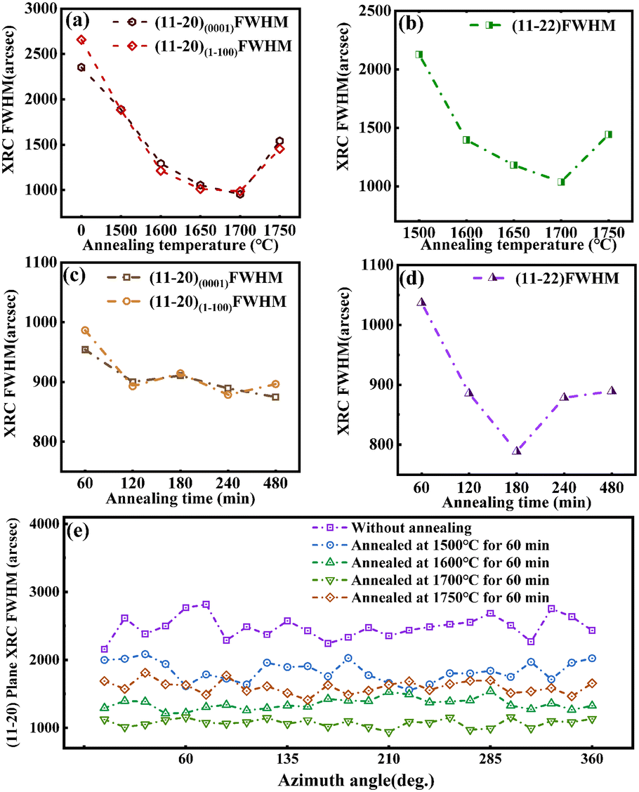 | ||
| Fig. 1 (a) The FWHMs of (11−20)[10−10] and (11−20)[0001] plane XRC and (b) the FWHMs of (11−22) plane XRC for the a-AlN annealed at different temperatures for 60 min. (c) The FWHMs of (11−20)[10−10] and (11−20)[0001] plane XRC and (d) the FWHMs of (11−22) plane XRC for the a-AlN annealed at 1700 °C with different annealing times. (e) The FWHM of (11−20) XRC of a-AlN as a function of azimuth angles, for the a-AlN annealed at different temperature for 60 min. | ||
To investigate the effect of annealing time on the crystal quality of a-AlN annealed at 1700 °C, the FWHMs of (11−20)[0001]/(11−20)[10−10] and (11−22) plane XRC for the a-AlN annealed at 1700 °C with different annealing time are summarized in Fig. 1(c) and (d). Fig. 1(c) illustrates that the FWHMs of (11−20)[0001]/(11−20)[10−10] plane XRC are reduced slightly (no more than 10%) with the annealing time increasing from 60 min to 480 min. These results indicate that both the tilt and twist mosaics of the a-AlN layers are lightly influenced by the annealing time. Fig. 1(d) shows that the minimal FWHM of (11−22) plane XRC reaches 810 arcsec for the a-AlN annealed at 1700 °C for 180 min.
The modified Williamson–Hall model is an effective way to measure the lateral coherence length (LCL) of crystals, and thus the BSFD can be calculated. The Williamson–Hall-type peak width plots contain the (h0–h0) (h = 1, 2, 3) plane XRC scan reflections, but the FWHM of (30−30) plane XRC is not considered in the calculation (due to ref. 24). The LCL was estimated by fitting the FWHM of the XRC diffraction peak of (10−10) and (20−20). The equation for W–H analysis can be expressed as follows:
 | (1) |
| Sample | Off-axis XRD ω-scan FWHM (arcsec) | W–H plot | ||
|---|---|---|---|---|
| (10−10) | (20−20) | c-Axis LCL (nm) | BSF density (×104 cm−1) | |
| a-AlN templates annealed at different temperatures for 60 min | ||||
| 1500 °C | 1933 | 1054 | 368 | 2.71 |
| 1600 °C | 1227 | 835 | 416 | 2.40 |
| 1650 °C | 1076 | 954 | 1130 | 0.88 |
| 1700 °C | 1022 | 964 | 1333 | 0.74 |
| 1750 °C | 1202 | 964 | 675 | 1.48 |
| a-AlN templates annealed at 1700 °C for different time | ||||
| 60 min | 1022 | 964 | 1333 | 0.74 |
| 120 min | 1008 | 903 | 1549 | 0.64 |
| 180 min | 1011 | 910 | 1797 | 0.55 |
| 240 min | 982 | 864 | 1524 | 0.65 |
| 480 min | 964 | 838 | 1431 | 0.69 |
| Samples (method) | Thickness | FWHM (arcsec) | BSFDs (cm−1) | Ref. |
|---|---|---|---|---|
|
a-AlN (HVPE:NH3 preflow) |
1 μm | (11−20)//[1−100]:1210 |
— | 16 |
| (11−20)//[0001]:1260 |
||||
|
a-AlN (MOCVD and HVPE:NH3 preflow and annealing) |
10 μm | (11−20)//[1−100]:660 |
— | 9 |
| (11−20)//[0001]:700 |
||||
| a-AlN (MOCVD: two-step growth) | 2 μm | (11−20)//[1−100]:1430 |
— | 17 |
| (11−20)//[0001]:2100 |
||||
| m-AlN (magnetron sputtering and HTA) | 275 nm | (10−10)//[11−20]:684 |
5.0 × 10³ | 11 |
| (10−10)//[0001]:864 |
||||
| m-AlN (MOCVD and HTA) | 550 nm | (10−10)//[11−20]:800 |
1.5 × 10⁴ | 7 |
| (10−10)//[0001]:1030 |
||||
| a-AlN (magnetron sputtering and HTA) | 200 nm | (11−20)//[1−100]:914 |
5.5 × 10³ | This work |
| (11−20)//[0001]:910 |
In a-plane III-nitride materials, it has been reported that the BSFs, bounded by Frank–Shockley PDs, are the main contributors to the defect density because the formation of the BSFs and PDs is more energetically favorable than that of the perfect dislocations. Thus, the behavior of BSFs can be reflected by the cross-sectional TEM results of both BSFs and PDs. The cross-sectional TEM along the [1−100] axis of the a-AlN samples without/with 1700 °C annealing was taken as g = 11−20 to analyze the behavior of the SFs. The invisible criterion of the BSFs and PSFs is g × R = 0 or an integer, where the R represents the displacement vector. The BSFs are bounded with the PDs, and the invisible criterion of the PDs is g × b < 1/3, where b represents the Burgers vectors of dislocations. The PSFs (R = ±1/2〈101−1〉), BSFs and PDs (R or b = ±1/6〈20−23〉 or ±1/3〈10−10〉) can be observed when adopting g = 11−20. The BSFs bounded by PDs are aligned with relatively long lengths along the [1−100] direction and the PSFs should show a band contrast according to the relationship between the stacking fault arrangement and crystal orientation.27 The invisible criteria for perfect dislocations (b = ±〈0001〉 for edge dislocation and b = ±1/3〈11−20〉 for screw dislocation in a-plane III-nitrides) is g × b = 0. Thus, the edge dislocation is invisible and the dislocation with screw components is visible when adopting g = 11−20. However, based on the former work from ref. 27, the density of the perfect dislocation is much lower than that of the BSFs (PDs), because the formation of BSFs bound by PDs is energetically favorable compared to perfect dislocations. As a result, the lines in the cross-sectional TEN image are mainly contributed by BSFs and PSFs. The cross-sectional TEM image of the a-AlN without annealing is exhibited in Fig. 2(a), and there is a high density of vertical defects propagating through the a-AlN film and the density is too high to distinguish each BSF or dislocation. The defects mainly propagate along the growth direction. After annealing at 1700 °C, the density of the defects decreased significantly as shown in Fig. 2(b). The defects in the blue rectangle are the PSFs because of the band contrast. However, the projection length of PSFs on the section surface is not a certain value, which makes it hard to analyze the behavior of PSFs during HTA. Based on the fact that the BSFs should propagate to the sample surface or annihilate with each other, the defects in Fig. 2(b) can be further determined except for the fragmentary area.28,29 The defects in the yellow and red rectangle are the BSFs (or PDs), and the interrupted defect lines without the mark are perfect dislocations. Because the perfect dislocation can bend to the outside of the section, which makes it seems interrupted in the TEM images. The defects in the red rectangle are considered to be the BSFs (or PDs) because of the relatively long lengths. It can be clearly observed that the two BSFs in the red rectangle gradually bend and annihilate each other. The defects lines (two pairs of BSFs) in the yellow rectangle also indicate that the defects (PSFs or BSFs) will annihilate with each other during high-temperature annealing. It can be found that the two outside BSFs and the two inside BSFs annihilate each other, respectively. The reason for this phenomenon is extrapolated that the lattice sequence between one pair of BSFs is different from the overall crystal, and the HTA process can provide enough driven energy to rearrange the lattice sequence and thus annihilate the BSFs. As results, the annihilation mode for one pair of BSFs is shown in the red rectangle, and the annihilation mode for the two pairs of BSFs is shown in the yellow rectangle.
 | ||
| Fig. 2 Cross-sectional TEM images of a-AlN templates (a) without annealing and (b) annealed at 1700 °C for 60 min, which are taken near the [1−100] axis with g = 11−20. | ||
In order to explain the mechanism of the reduction of BSFs during HTA process, the transition energy barriers are investigated during the elimination of the I1-type BSF, which is the majority of BSFs (proportion >90%) in a-AlN.30,31 The wz-AlN supercell is built as shown in structure A of Fig. 3, and the stacking sequence of atoms is [⋯AaBbAaBb⋯] along the [0001] direction (capital letters correspond to Al, lowercase letter correspond to N). The I1-type BSF is built with the stacking sequence of [⋯AaBbCcBbCcBbAaBb⋯] along the [0001] direction (denoted as 2-layer-I1-AlN, as shown in structure I of Fig. 3). The minimum energy pathway from the 2-layer-I1-AlN to wz-AlN was calculated by the climbing-image nudged elastic band (CI-NEB) method. The energy barriers and the atomic structures during the reaction are shown in Fig. 3. The computational details are shown in the ESI.†23 The atoms that tend to move to the new equilibrium positions are circled in yellow dashed rectangles, and the positions of the BSFs' boundaries (the PDs) are marked by translucent black lines, approximately.
 | ||
| Fig. 3 Top: The minimum energy pathway during the reaction from wz-AlN (A) to 2-layer-I1-AlN (I). Bottom: The corresponding structures of the energy barriers and local metastable states. The locations of the SFs are marked by grey lines and the orange-coloured rectangles are used to mark the representative atoms with obvious displacement. | ||
The calculated results indicate that the total energy of 2-layer-I1-AlN is about 0.39 eV higher than that of the perfect wz-AlN. During the elimination of the stacking fault (from structures I to A), there are four local energy barriers (structure B, D, F, H) that are about 5.10–5.49 eV higher than the initial state of wz-AlN, two metastable states (structure C, G) that are about 1.85 eV higher than wz-AlN, and a local stable state (structure E) that is 0.31 eV higher than wz-AlN. Structure E has the same stacking sequence with the I3-type BSF of AlN [⋯AaBbCcBbAaBb⋯]. It can be inferred that the I3-type BSF is the intermediate state during the elimination of the I1-type BSF. The highest energy barrier to eliminate the I1-type stacking default is 5.032 eV (from the structure I to H) and the highest energy barrier to form the I1-type stacking fault is 5.204 eV (from structure A to I). It means that when the driven energy (mainly obtained from the annealing temperature) is higher than 5.032 eV and lower than 5.204 eV, the annihilation of I1-type stacking faults is the main reaction. As exhibited in Fig. 3, when the BSFs are observed from (11−20) and (1−100) directions, the two BSFs will bend and move closer to each other during HTA, which is consistent with the TEM results as shown in Fig. 2(b). Driven by high temperature, the atoms of structure I tend to vibrate and finally move to the locations, which will provide minimum system energy. During the process, some energy barriers will be overcome to reach the minimum energy. The locations of the SFs are marked by grey lines and the orange-coloured rectangles are used to mark the representative atoms with obvious displacement. From the structure I to structure E, as shown in Fig. 3, the atoms at Cc positions near the orange-coloured rectangles move to the Aa positions, which makes the two I1-type stacking faults move closer to each other and even turn into I3-type stacking faults with the lattice sequence of [⋯AaBbCcBbAa⋯]. The related phenomenon is shown in the red rectangle in Fig. 2 that the top of two stacking faults is closer than the bottom of the two stacking faults. From structure E to structure A, the atoms at Cc positions of the I3-type stacking fault [⋯AaBbCcBbAa⋯] will also move to Aa positions [⋯AaBbAaBbAa⋯] and thus annihilate the stacking faults. However, when the annealing temperature is higher than a certain threshold temperature and the driven energy is higher than the highest energy barrier from structure A to structure I (5.204 eV), the I1-type stacking defaults will be formed, which is a contrary process to the process of stacking fault annihilation. As a result, with the increasing annealing temperature, the BSFD should show decreasing tendency at first and then convert to an increasing tendency, which is in agreement with the variation tendency of the XRC results as shown in Table 1 and Fig. 1.
The stress state of the AlN epilayers should be changed when the recrystallization process occurs in a-AlN templates because the annihilation of BSFs attenuates the BSF's function of releasing the stress induced by the mismatch between AlN and sapphire substrate.32,33 To verify the above conclusion, the Raman spectra of a-AlN under different annealing conditions were taken and shown in Fig. 4. The dotted lines in Fig. 4 (670.8 and 657.4 cm−1) are the phonon frequencies of E1(TO) and E2(high) for strain-free AlN, respectively.34–36 Here, we extracted the E1(TO) and E2(high) peak positions of all the a-AlN samples from the Raman curves in Fig. 4(a) and (c), and the results are summarized in Fig. 4(b) and (d) respectively. From Fig. 4(b) and (d), it can be observed that the position of the E2(high) peak for the a-AlN template without annealing is lower than 657.4 cm−1, which indicates that the as-sputtered a-AlN film is under tensile stress. The Raman peaks of a-AlN templates blue shifted after the HTA process, which meant the increase of compressive stress in the a-AlN layer. Combining the results of Fig. 4(b) and (d) with the results of Fig. 1 and Table 1, it can be found that the blue-shift of the Raman peaks increases with the decreasing BSFD, which means that the compressive stress was accumulated with the decrease in BSFD.37 Hence, the maximum compressive strain was generated in the a-AlN sample annealed at 1700 °C for 180 min. Correspondingly, according to XRC results, the a-AlN template annealed at 1700 °C for 180 min has the largest grain size and lowest BSFD, which is well consistent with the results of the Raman spectra.38
 | ||
| Fig. 4 (a) Room Raman spectra and (b) the positions of the E1(TO) and E2(high) peaks of a-AlN annealed at different temperatures for 60 min. (c) Room Raman spectra and (d) the positions of the E1(TO) and E2(high) peaks of a-AlN annealed at 1700 °C with different annealing times. | ||
Conclusions
In summary, the annihilation mechanism of BSFs during the HTA process was investigated in the present work. The XRC measurement and the modified Williamson–Hall model calculation results demonstrated that the optimal a-AlN with a minimal BSFD of ∼5500 cm−1 was obtained at an annealing temperature of 1700 °C for 180 min. Additionally, the calculated LCL and the cross-sectional TEM results proved that the recrystallization took place during the HTA process. To uncover the annihilation mechanism of BSFs, the minimum energy pathway of the I1-type BSF elimination process was investigated by first-principle calculations. The results showed that two I1-type stacking faults transformed into one I3-type stacking fault as the intermediate state and then were annihilated. Furthermore, the first-principle calculation and Raman spectra results also well explained the BSFD variation tendency that decreases at first and then increases with the rise in the annealing temperature. The work provides further comprehension of the improvement mechanism of a-AlN by the HTA method, which is vital for the fabrication of high-quality a-AlN and related devices.Author contributions
Xiaojuan Sun contributed to data curation, formal analysis, and writing review and editing; Jiaen Sui, JianWei Ben, and Hang Zang contributed to methodology and writing – original draft; Ke Jiang and Shunpeng Lv contributed to the investigation; Shanli Zhang contributed to the project administration; Zhiming Shi and Tong Wu contributed to the resources; Dabing Li contributed to conceptualization and funding acquisition.Conflicts of interest
There are no conflicts to declare.Acknowledgements
This work was supported by the National Key R&D Program of China (grant number 2022YFB3605103); National Natural Science Foundation of China (grant numbers U22A2084, 62004196, 62121005, 12234018, 62004127 and 61827813); Youth Innovation Promotion Association of Chinese Academy of Sciences; and Youth Talent Promotion Project of the Chinese Institute of Electronics (grant number 2020QNRC001).Notes and references
- K. Jiang, X. Sun, Z. Shi, H. Zang, J. Ben, H. Deng and D. Li, Light: Sci. Appl., 2021, 10, 69, DOI:10.1038/s41377-021-00503-y
.
- W. Yao, F. Li, L. Wang, S. Liu, H. Wei, S. Yang and Z. Wang, CrystEngComm, 2020, 22, 3198, 10.1039/D0CE00147C
- Y. Sun, F. Xu, N. Zhang, J. Lang, J. Wang, B. Liu, L. Wang, N. Xie, X. Fang, X. Kang, Z. Qin, X. Yang, X. Wang, W. Ge and B. Shen, CrystEngComm, 2021, 23, 1201, 10.1039/D0CE01491E
- C. Blumberg, F. Wefers, F.-J. Tegude, N. Weimann and W. Prost, CrystEngComm, 2019, 21, 7476, 10.1039/C9CE01151J
- H. Kim, J. Lin and H. Jiang, Appl. Phys. Lett., 1998, 73, 3426, DOI:10.1063/1.122786
- H. Masui, S. Nakamura, S. Denbaars and U. Mishra, IEEE Trans. Electron Devices, 2010, 57, 88, DOI:10.1109/TED.2009.2033773
- D. Dinh, H. Amano and M. Pristovsek, J. Cryst. Growth, 2018, 502, 14, DOI:10.1016/j.jcrysgro.2018.09.001
- M. Esmaeili, H. Haratizadeh and M. Gholami, Phys. B, 2009, 404, 4233, DOI:10.1016/j.physb.2009.08.019
- C. Lin, S. Tamaki, Y. Yamashita, H. Miyake and K. Hiramatsu, Appl. Phys. Express, 2016, 9, 081001, DOI:10.7567/APEX.9.081001
- D. As and C. Mietze, Phys. Status Solidi A, 2013, 210, 474, DOI:10.1002/pssa.201200653
- D. Dinh, N. Hu, Y. Honda, H. Amano and M. Pristovsek, J. Cryst. Growth, 2018, 498, 377, DOI:10.1016/j.jcrysgro.2018.07.015
- P. Vennéguèsa and Z. Bougrioua, Appl. Phys. Lett., 2006, 89, 111915, DOI:10.1063/1.2353810
- F. Ren, Z. Hao, C. Zhang, J. Hu and Y. Luo, Chin. Phys. Lett., 2010, 27, 068101, DOI:10.1088/0256-307X/27/6/068101
- J. Wu, K. Okuura, K. Fujita, K. Okumura, H. Miyake and K. Hiramatsu, J. Cryst. Growth, 2009, 311, 4473, DOI:10.1016/j.jcrysgro.2009.08.009
- R. Miyagawa, H. Miyake and K. Hiramatsu, Phys. Status Solidi, 2010, 7, 2107, DOI:10.1002/pssc.200983601
- C. Lin, D. Yasui, S. Tamaki, H. Miyake and K. Hiramatsu, Jpn. J. Appl. Phys., 2016, 55, 05FA12, DOI:10.7567/JJAP.55.05FA12
- M. Jo and H. Hirayama, Jpn. J. Appl. Phys., 2016, 55, 05FA2, DOI:10.7567/JJAP.55.05FA02
- N. Okada, N. Kato, S. Sato, T. Sumii, N. Fujimoto, M. Imura, K. Balakrishnan, M. Iwaya, S. Kamiyama, H. Amano, I. Akasaki, T. Takagi, T. Noro and A. Bandoh, J. Cryst. Growth, 2007, 300(1), 141, DOI:10.1016/j.jcrysgro.2006.11.025
- H. Miyake, G. Nishio, S. Suzuki, K. Hiramatsu, H. Fukuyama, J. Kaur and N. Kuwano, Appl. Phys. Express, 2016, 9, 025501, DOI:10.7567/APEX.9.025501
- Y. Mogami, A. Osawa, K. Ozaki, Y. Tanioka, A. Maeoka, Y. Itokazu, S. Kuwaba, M. Jo, N. Maeda, H. Yaguchi and H. Hirayama, Phys. Status Solidi B, 2020, 257, 1900590, DOI:10.1002/pssb.201900590
- K. Nagamatsu, X. T. Liu, K. Uesugi and H. Miyake, Jpn. J. Appl. Phys., 2019, 58, sccc07, DOI:10.7567/1347-4065/ab07a1
- H. Miyake, C. Lin, K. Tokoro and K. Hiramatsu, J. Cryst. Growth, 2016, 456, 155, DOI:10.1016/j.jcrysgro.2016.08.028
- G. Henkelman, B. Uberuaga and H. Jonsson, J. Chem. Phys., 2000, 113, 9901, DOI:10.1063/1.1329672
- M. Moram, C. Johnston, J. Hollander, M. Kappers and C. Humphreys, J. Appl. Phys., 2009, 105, 113501, DOI:10.1063/1.3129307
- J. H. Kim, S. M. Hwang, K. H. Baik and J. H. Park, J. Semicond. Technol. Sci., 2014, 14, 557, DOI:10.5573/JSTS.2014.14.5.557
- C. Wang, Y. Jiang, J. Die, S. Yan, X. Hu, W. Hu, Z. Ma, Z. Deng, H. Jia and H. Chen, CrystEngComm, 2019, 21, 2747, 10.1039/c8ce01988f
- B. Kong, Q. Sun, J. Han, I. Lee and H. Cho, Appl. Surf. Sci., 2012, 258, 2522, DOI:10.1016/j.apsusc.2011.10.086
- Q. Sun, B. H. Kong, C. Yerino, T. Ko, B. Leung, H. Cho and J. Han, J. Appl. Phys., 2009, 106, 123519, DOI:10.1063/1.3272790
- S. Xu, J. Zhang, L. Yang, X. Zhou, Y. Cao, J. Zhang, J. Xue, Z. Liu, J. Ma, F. Bao and Y. Hao, J. Cryst. Growth, 2011, 327, 94, DOI:10.1016/j.jcrysgro.2011.06.013
- C. Stampfl and C. Van de Walle, Phys. Rev. B: Condens. Matter Mater. Phys., 1998, 57, R15052(R), DOI:10.1103/PhysRevB.57.R15052
- M. Pristovsek, M. Frentrup, T. Zhu, G. Kusch and C. Humphreys, CrystEngComm, 2021, 23, 6059, 10.1039/d1ce00627d
- R. Chierchia, T. Bottcher, H. Heinke, S. Einfeldt, S. Figge and D. Hommel, J. Appl. Phys., 2003, 93, 8918, DOI:10.1063/1.1571217
- A. Claudel, V. Fellmanna, I. Gelard, N. Coudurier, D. Sauvage, M. Balaji, E. Blanquet, R. Boichot, G. Beutier, S. Coindeau, A. Pierret, B. Attal-Tretout, S. Luca, A. Crisci, K. Baskar and M. Pons, Thin Solid Films, 2014, 573, 140, DOI:10.1016/j.tsf.2014.11.022
- X. Yao, G. Wang, H. Tu, S. Liu, M. Yang, Z. Kong, Y. Shao, Y. Wu and X. Hao, CrystEngComm, 2021, 23, 4946, 10.1039/d1ce00366f
- V. Davydov, Y. Kitaev, I. Goncharuk, A. Smirnov, J. Graul, O. Semchinova, D. Uffmann, M. Smirnov, A. Mirgorodsky and R. Evarestov, Phys. Rev. B: Condens. Matter Mater. Phys., 1998, 58, 12899, DOI:10.1103/PhysRevB.58.12899
- X. Yao, Z. Kong, S. Liu, Y. Wang, Y. Shao, Y. Wu and X. Hao, Materials, 2022, 15, 8791, DOI:10.3390/ma15248791
- H. J. Trodahl, F. Martin, P. Muralt and N. Setter, Appl. Phys. Lett., 2006, 89, 061905, DOI:10.1063/1.2335582
- T. Bottcher, S. Einfeldt, S. Figge, R. Chierchia, H. Heinke, D. Hommel and J. Speck, Appl. Phys. Lett., 2001, 78, 1976, DOI:10.1063/1.1359780
Footnote |
| † Electronic supplementary information (ESI) available: Symmetric ω–2θ XRD scans, Fig. S1. The XRD ϕ scan result of (11−22) plane a-AlN template without annealing, Fig. S2. W–H plots of a-AlN films, Fig. S3. The calculation details of the CI-NEB. See DOI: https://doi.org/10.1039/d2ce01654k |
| This journal is © The Royal Society of Chemistry 2023 |