
 Open Access Article
 This Open Access Article is licensed under a Creative Commons Attribution-Non Commercial 3.0 Unported Licence
Energy transfer and charge transfer between semiconducting nanocrystals and transition metal dichalcogenide monolayers
Aswin
Asaithambi
a,
Nastaran
Kazemi Tofighi
a,
Michele
Ghini
 ab,
Nicola
Curreli
*a,
P. James
Schuck
c and
Ilka
Kriegel
*a
ab,
Nicola
Curreli
*a,
P. James
Schuck
c and
Ilka
Kriegel
*a
aFunctional Nanosystems, Istituto Italiano di Tecnologia, Via Morego 30, Genova, 16163, Italy. E-mail: nicola.curreli@iit.it; ilka.kriegel@iit.it
bNanoelectronic Devices Laboratory, École Polytechnique Fédérale de Lausanne (EPFL), Lausanne, 1015, Switzerland
cDepartment of Mechanical Engineering, Columbia University, New York, NY, USA
First published on 2nd May 2023
Abstract
Nowadays, as a result of the emergence of low-dimensional hybrid structures, the scientific community is interested in their interfacial carrier dynamics, including charge transfer and energy transfer. By combining the potential of transition metal dichalcogenides (TMDs) and nanocrystals (NCs) with low-dimensional extension, hybrid structures of semiconducting nanoscale matter can lead to fascinating new technological scenarios. Their characteristics make them intriguing candidates for electronic and optoelectronic devices, like transistors or photodetectors, bringing with them challenges but also opportunities. Here, we will review recent research on the combined TMD/NC hybrid system with an emphasis on two major interaction mechanisms: energy transfer and charge transfer. With a focus on the quantum well nature in these hybrid semiconductors, we will briefly highlight state-of-the-art protocols for their structure formation and discuss the interaction mechanisms of energy versus charge transfer, before concluding with a perspective section that highlights novel types of interactions between NCs and TMDs.
Hybrid structures of semiconducting nanoscale matter can offer exciting new opportunities for novel optoelectronic and photonic devices.1 With the discovery of layered transition metal dichalcogenides (TMDs) a new family of semiconducting low-dimensional structures has emerged.1–4 The atomic van der Waals interactions allow exfoliating them into flakes composed of a single two-dimensional (2D) layer.2,5 The transition from a multilayer ensemble to a single, atomically thin monolayer (2D TMD) occurs with a transition from an indirect semiconductor to a direct bandgap semiconductor with bandgaps in the visible range, e.g. 1.8 eV for 2D MoS2.2 The single layer nature and large surface area brings along challenges, but also unique opportunities. The confinement in one direction makes them suitable quantum well structures.6 In fact, TMDs, such as 2D MoS2 can sustain tightly bound negative (or positive) trions, quasiparticles composed of two electrons and one hole (vice versa), as a consequence of the significantly enhanced Coulomb interactions arising from reduced dielectric screening above and below the monolayer structure.4 High carrier mobility, carrier density in the order of 1012 cm−2, and their semiconducting nature with a bandgap in the visible spectral range make them interesting candidates for electronic and optoelectronic devices, such as transistors or photodetectors.7–11 The large surface and high interaction area of 2D TMDs highlight also the option to combine the atomically thin monolayer with other nanoscale structures.12–15 In particular, hybrid nanostructures made of nanocrystals (NCs) with quasi zero-dimensional (0D) extension found great attention in recent years due to the ease of fabrication, considering that a variety of 0D semiconductors, are synthesized in solution.16–18 Thus, the physical connection of the 0D and 2D material can be induced by solution processing, such as drop casting or spin coating.13,16,19,20 Moreover, 0D NCs offer a variety of parameters to define their optical properties by controlling material (i.e., semiconducting properties), size (i.e., quantum confined bandgap), hybrid nanostructures (i.e., band alignments), shape (i.e., control over the electron wave function), or doping.21–24 The high absorption cross-section of semiconductor NCs makes them attractive components in hybrid 0D/2D structures for phototransistors or photodetectors, but also photovoltaics or photocatalysis,25,26 as their exceptional optical properties can be combined with the carrier transport properties of TMDs. Thus, the study of 0D/2D hybrid structures and their fundamental interaction mechanism is of major interest. The emergence of 0D/2D hybrid structures has sparked a broad research interest in interfacial carrier dynamics, including energy transfer (ET) and charge transfer (CT), which are ubiquitous phenomena and crucial processes that control the interfacial properties of 0D/2D heterostructures.27,28 Although the interfacial carrier dynamics have been extensively studied in a variety of donor–acceptor systems for several decades, such as organic semiconductor interfaces and biological molecules,29,30 0D/2D systems are a brand-new platform in the quantum limit with strong quantum confinement and coherence effect.
In the following article, we will summarize recent works on the combined hybrid system of 0D/2D NC/TMD semiconductors focusing on the different interaction mechanisms. We will briefly highlight state-of-the-art protocols for their hybrid structure formation and discuss the interaction mechanisms of energy versus charge transfer, with a focus on the quantum well nature and the observation of tightly bound exciton complexes in these structures. We will discuss on recent advances in device design based on these heterostructures. In the last part of this paper, we give a perspective on new routes toward new hybrid interaction exploiting the particular properties of TMDs for novel and improved device design.
Background on the heterostructure of 0D and 2D materials
TMDs are a class of layered semiconducting materials with strong in-plane bonding and weak out-of-plane bonding.1 Typically, monolayer 2D TMDs (with a thickness of around 0.7 nm) and bilayer TMDCs (with a thickness of around 1.5 nm) can be distinguished from the optical micrograph due to different optical contrast.31 More conclusive characterization of the number of layers can be obtained from atomic force microscopy (AFM) or indirectly by Raman and photoluminescence (PL) spectroscopy.32–35 In fact, the bilayer TMD with its indirect bandgap has lower PL intensities with respect to the 2D TMDs and also the separation of the Raman peaks of Eg (in-plane) and A1g (out-of-plane) is a clear indication for the number of layers.33,36 The high surface area of 2D TMDs (Fig. 1(a)) allows contacting them easily with solution-based materials, such as 0D nanocrystals. Here we discuss in particular 0D semiconductor nanocrystals, which possess exciting properties due to the large surface-to-volume ratio and/or quantum confinement effects. Depending on the material of choice and their size, 0D semiconductor nanocrystals display photoluminescence emission in the spectral range from the ultraviolet to the infrared region (e.g., III–V and II–VI semiconductors, such as GaN, GaAs, PbSe, PbS, CdSe, PbTe, InAs or CsPbBr3),37–44 while others display plasmonic response due to high free carrier densities (e.g. doped metal oxides, such as, Sn:In2O3, Ga:ZnO, Al:ZnO).45 Typical transmission electron microscope images of CsPbBr3 and Sn:In2O3 (ITO) nanocrystals are shown in Fig. 1(b). Finally, 2D materials and 0D materials can be put together to form hybrid heterostructures (Fig. 1(c)). | ||
| Fig. 1 (a) Optical micrograph of exfoliated MoS2 showing different optical contrast for monolayer (1L), bilayer (2L) and multilayer (3L). (b) Typical transmission electron micrographs of CsPbBr3 nanocrystals (top) and ITO (bottom). (c) Typical scanning electron micrograph of spin-coated nanocrystals that forms a uniform layer on top of monolayer TMDC.13 (d) Schematic representation of different processing steps occurring during the deposition of colloidal 0D nanocrystals via spin coating. First, a drop of dispersed 0D nanocrystals is deposited on the substrate (i). Then the spinning is accelerated (ii) until it reaches a desired angular speed (ω). In the spin-off stage (iii) the rotation speed is kept constant to eject any excess solution and leave a thin layer of coating on the substrate. The two final stages, spin-off (iii) and evaporation (iv), occur simultaneously as the spinning induces an airflow that accelerates the evaporation of the solvent. | ||
Production of 2D materials
Research on atomically thin materials has a rich historical background.46 However, only in 2004, Geim and Novoselov successfully used mechanical exfoliation to obtain single-layer graphene from graphite crystals47 and 2D materials gained widespread attention. Since then, the field of 2D materials has experienced rapid development with the emergence of various new 2D materials and preparation methods.48,49 The mainstream methods for preparing 2D materials can be categorized into two categories: top-down methods and bottom-up methods. Top-down methods involve obtaining 2D materials directly from 3D bulk crystals with a layered structure, such as mechanical exfoliation and liquid exfoliation.49 On the other hand, bottom-up methods involve synthesizing 2D materials at the molecular level through chemical reactions using appropriate precursors, such as chemical vapor deposition (CVD).49Top-down approach
This method involves the application of mechanical force to bulk crystals, which eliminates the van der Waals forces between layers without disrupting the in-plane crystal structure, resulting in the formation of nanoflakes/microflakes with atomic thickness preserving the crystalline integrity. Theoretically, this method can be applied to any natural crystal with an atomic layered structure to obtain corresponding single-layer 2D materials. Conventional mechanical exfoliation (CME) is a commonly used approach in which a bulk crystal is repeatedly pressed onto an adhesive surface and then peeled off using a clean silicon wafer, resulting in the transfer of crystal flakes onto the target substrate.48,49 Optical microscopy can be used to locate few-layer or single-layer crystals. The CME method has the advantage of directly obtaining 2D material flakes from natural crystals, thereby avoiding the introduction of defects during synthesis and contamination from chemical reagents. However, CME has some limitations that restrict its potential applications. Firstly, not all crystals with a layered structure can be easily exfoliated to obtain few-layer or single-layer nanosheets using this method. For example, crystals with ionic bond characteristics, such as hexagonal boron nitride (h-BN), have stronger van der Waals forces between layers compared to graphite, making it difficult to peel off single-layer nanosheets from natural h-BN crystals.50 Similarly, crystals with more valence electrons and polar covalent bonds, as in the case of TMDs, also have tightly coupled layers, posing challenges for exfoliation.51 Lastly, the low yield and non-uniformity in the size (lateral size of few μm), thickness, and shape combined with the demanding operation and subsequent manual screening involved in CME can lead to low production efficiency. Some of these limitations can be addressed by enhancing the bonding strength between the substrate and the 2D material, improving the exfoliation yield. For instance, adhesion between 2D material and the substrate can be improved using a strong electrostatic field and/or heat treatment between the substrate and the bulk crystal.52 However, stringent requirements are needed for the substrate surface, which restrict the peeling of 2D materials to specific substrates, and it may not be effective for all bulk crystals. Moreover, the high-temperature heat treatment can cause oxidation or sublimation of less chemically stable crystals, which complicates the process and limits its wide application.In recent years, researchers have also developed new exfoliation methods for preparing 2D materials with higher yields and larger lateral dimensions. This approach, called metal-assisted exfoliation (MAE), exploits the affinity between certain metals and 2D materials, where a flat metal surface obtained by a deposition process is used to peel off 2D material flakes from the original crystal.52 For example, Huang et al.,53 and Liu et al.,54 modified the mechanical exfoliation method by creating atomically flat gold layers on polymer supports, resulting in the exfoliation of monolayers on the centimeter scale. The key step in the process is the deposition of an ultraflat gold tape, which serves as the exfoliation substrate. The gold tape is obtained through a template-stripping technique, where a thin gold film is evaporated onto an ultraflat surface of a highly polished silicon wafer. The gold film is then stripped off the substrate using thermal release tape and a polyvinylpyrrolidone interfacial layer, leaving behind an ultraflat gold surface templated by the flat substrate with roughness on the Å scale. This ultraflat gold tape allows for intimate and uniform vdW contact between the gold and the 2D vdW crystal surface, enabling the exfoliation of complete monolayers. One of the key advantages of the MAE method is the ability to obtain macroscopic monolayers with dimensions limited only by the sizes of the bulk crystals. This represents a significant increase in lateral sizes and monolayer yields by two to three orders of magnitude compared to conventional methods, such as the CME. Moreover, the MAE process transforms the stochastic nature of the CME method into a deterministic and quantitative process, making it highly reproducible and suitable for mass production. The resulting macroscopic monolayers obtained from the MAE method are comparable in quality to microscopic monolayers obtained from conventional methods.
Liquid phase exfoliation (LPE) is another technique in the realm of “top-down” methods for efficient preparation of 2D materials. This method employs a liquid medium to directly exfoliate bulk crystals into nanosheets of 2D materials through specific treatments.55,56 Solvents with suitable surface energy can prevent the exfoliated nanosheets from aggregating and ensure their independent stability. In comparison to CME, LPE exhibits greater potential for mass production capacity. Typically, the LPE method requires various assisted treatments for the raw materials. For instance, in the LPE process aided by mechanical force, bulk crystals are dispersed in a specific liquid such as N-methyl-2-Pyrrolidone or isopropanol for TMDs, and mechanical interactions such as sonication and shear force are applied to efficiently obtain 2D materials. LPE technology is widely employed in laboratory and industrial production due to its efficient and economical process, high yield, and standardized operation, which address the challenge of stabilizing 2D materials in solvents. However, the preparation of large-area 2D materials through LPE is challenging as the in-plane covalent bonds can be easily broken during the process, resulting in samples with inherent defects that limit their applications. In theory, LPE is not suitable for studying stacked structures of 2D materials. Nevertheless, in recent years, the emergence of 2D material ink technology has enabled the use of LPE for producing inkjet-printed heterojunctions, exhibiting significant potential.55,56
Bottom-up approach
In the field of synthesizing 2D materials, chemical vapor deposition (CVD) has emerged as a conventional technology widely used for mass production of large-area, high-quality 2D materials.57 In contrast CME and LPE, which suffer from low yield and low quality, CVD offers a coordinated approach to achieve high-quality materials with efficient and consistent processes through precise control of parameters such as temperature, pressure, and gas atmosphere. The general growth process of TMDs by CVD involves gaseous mass transfer of atoms. CVD allows for the synthesis of single-layer, heterojunction, and multilayer heterojunction structures by controlling these parameters. In recent decades, CVD has rapidly developed and is considered the most promising method for preparing ultrathin 2D materials. Currently, wafer-scale TMDs and meter-sized single-crystal graphene can be synthesized in the laboratory using CVD with reasonable parameter control.57 The use of salt-assisted synthesis technology and gas-phase precursor metallographic limited dissolution technology has expanded the range of 2D materials that can be synthesized by CVD.58 Despite these advancements, CVD-grown 2D materials still suffer from defects such as grain boundaries, wrinkles, impurities, and atomic vacancies, which can affect their performance compared to exfoliated 2D materials from bulk crystals. Additionally, the high reaction temperature and noble gas atmosphere required in CVD production processes result in higher costs compared to liquid phase-based synthesis methods.57,59Overall, despite these advances, there is still significant research that must be done to improve the fabrication techniques for 2D materials. In fact, it is still missing a method that include the production of 2D materials with both high quality and large lateral dimensions that is at the same time also scalable and cost-effective which remains a critical challenge.60
Synthesis of 0D materials
For 0D materials, synthesis techniques vary depending on the material type.61,62 Considering metal oxide nanoparticles (MONPs) as a case study, synthesis methods can be classified into two groups: (i) physical methods, such as ball milling, sputtering, laser ablation, electrospraying, and electron beam evaporation, and (ii) chemical methods, such as colloidal synthesis, non-thermal plasma assisted synthesis, sol–gel method, polyol method, hydrothermal method, co-precipitation method, microemulsion technique, and chemical vapor deposition.63–65 Physical methods follow a top-down strategy, where NPs are generated from the bulk counterpart of a material through systematic depletion. On the other hand, chemical methods primarily adopt a bottom-up approach, involving the assembly of atoms or molecules to form NPs of various sizes. The main advantage of chemical methods is that they enable the production of particles with well-defined size, dimension, composition, and structure, which are beneficial for various applications, including catalysis, sensing, and electronic devices. Typically, 0D materials such as MONPs growth involves the choice of precursors, ligands and reaction media which is usually a solvent with high boiling point. The precursors are introduced in a hot reaction media which promotes the nucleation and growth of the nanoparticles and the ligand passivates the surface to prevent aggregation. Time is a crucial parameter of the reaction which can influence the size of the nanocrystal. Similar techniques can be extended to other semiconductor nanocrystals such as halide perovskites, II–VI or III–V semiconductor nanocrystals.66Implementation of 0D/2D heterostructures
As discussed in the previous sections, 0D nanocrystals can be synthesized and dispersed in a colloidal solution, while 2D materials, such as TMDs, can be obtained through exfoliation or alternative methods to obtain atomically thin layers. The colloidal stability of 0D nanocrystals in solution can be facilitated by surfactants, enabling solution processing methods such as spin coating, drop casting, or others.13,16,67 Hence, a viable approach involves the fabrication of heterostructures by spin coating the 0D nanocrystals onto the 2D material. This approach presents a versatile and scalable method for depositing thin films of materials with precise control over thickness and coverage, as demonstrated in Fig. 1(d). The spin coating process can be optimized to achieve the desired thickness and coverage of the 0D nanoparticles on the 2D material. For example, the uniform distribution of 0D nanocrystals over the 2D TMD crystal can be achieved by choosing a suitable solvent, as well as tuning the dispersion's concentration and spin-coating parameters (acceleration, angular speed, spinning time). In this context, the tuning of nanocrystals’ concentration plays a crucial role, as the density and the uniformity of the nanocrystal films are largely affected by this parameter.13 Usually, higher spin speeds typically result in thinner films, while higher solution concentrations and viscosities can lead to increased nanoparticle coverage. First, a drop of colloidally dispersed 0D nanocrystals is deposited on the substrate. Depending on the concentration of the NC solution, the spin-coater is accelerated until it reaches the desired angular speed (ω). As a result, a thin coating layer is formed on the substrate and any excess solution is ejected during the spin-off stage by maintaining a constant ω. The spinning causes an airflow that speeds up the solvent evaporation, so the two final stages, spin-off and evaporation, happen simultaneously. The scanning electron micrograph in Fig. 1(c) shows the uniform distribution of nanocrystals on both the substrate and the 2D materials.13 The resulting 0D/2D heterostructure can exhibit unique properties that arise from the synergistic effects between the 0D nanoparticles and the 2D material. For example, the 0D nanoparticles can introduce localized electronic states, quantum confinement effects, or enhanced chemical reactivity, while the 2D material can provide a supportive matrix, offer unique electronic properties, or serve as a protective barrier for the nanoparticles. The properties of the 0D/2D heterostructure can be further customized through annealing or other thermal treatments, which can promote nanoparticle adhesion and interaction with the 2D material, or induce structural or phase transformations. These thermal treatments can be optimized to achieve desired modifications in the heterostructure, such as enhanced interfacial bonding, improved crystallinity, or improved electronic and optical properties. The choice of annealing temperature, duration, and atmosphere can be critical in influencing the final properties of the heterostructure, and it may require iterative experimentation and characterization to optimize the thermal treatment conditions for specific material combinations and applications.Interaction mechanisms between the 0D and 2D components
There have been plenty of reports on the integration of 0D/2D heterostructures with efficient interaction between the two materials.13,15,68–70 Choosing the appropriate 0D species can result in the alteration of specific properties of the underlying 2D material depending on the type of interactions between 0D and 2D material.13,15,71 Considering a simplified picture of a system composed by two materials A (donor) and B (acceptor) with different energy levels, we consider the 0D components as the donor material (A) and the 2D components as the acceptor material (B) (see Fig. 2(a) and (b)). The electronic states of the 0D/2D materials are approximated to be localized within the nanomaterials because of the weak inter-material coupling.72 Their band-edge energies can be used to evaluate the band alignment between the two species. A typical type-I band alignment is depicted in Fig. 1(c). The lowest energy conduction band minimum (CBM) and highest energy valence band maximum (VBM) of the two components are both found in the layer with the narrower bandgap. Conversely, a type-II band alignment refers to the case where the lowest CBM and highest energy VBM are located in different materials (Fig. 1(d)). The interaction mechanism is governed by two major processes: energy transfer and charge transfer. These processes occur following the photoexcitation and the creation of an electron in the CB and a hole in the VB of one of the components. In the CT mechanism (Fig. 2(a)), depending on the band alignment and on the type of interaction, several different processes can be observed. In the type-I heterostructure (Fig. 2(c)), if a CT is favored after photoexcitation of the wide-bandgap material, both charges, electrons and holes will be transferred from the 0D donor to the 2D acceptor. Hence, the carriers are directly trapped on the material 2D and might relax to form excitons. The confinement of electrons and holes in the same region facilitates their radiative recombination, which is desirable in light-emitting applications.73 In the case of the type-II heterostructure (Fig. 2(d)), the excitation of one material is followed by the selective transfer of holes (if the VBM of the acceptor is higher in energy with respect to the VBM of the donor), or of electrons (if the CBM of the acceptor is lower in energy with respect to the CBM of the donor). The CT is highly inefficient at long ranges as the efficiency is 12th power dependent on the distance between donor and acceptor.74,75 The separation of the electrons and holes to different layers can increase their lifetime, and is desired for applications in photovoltaics and photodetection.76 On the other hand, in ET (Fig. 2(b)) when the oscillations of a photo-induced electronic coherence on the donor 0D material are in resonance with the electronic bandgap of the acceptor 2D material, this energy is transferred from the 0D donor to the 2D acceptor with a specific efficiency.75Fig. 2(e) illustrates, how the photoexcited electron–hole pairs are primarily formed in the donor 0D material and then transferred to the acceptor material. The major route of ET known is Förster-type non-radiative energy transfer (FRET), which is a process of energy transfer that involves dipole–dipole Coulomb interactions between a donor and an acceptor material and is the underlying mechanism of numerous applications, including color tuning, biosensing, light-harvesting, and light generation.75,77–80 Due to the non-radiative nature of the interaction, photon emission and reabsorption are avoided, maintaining high energy conversion efficiency. The FRET rate is significantly affected by the center-to-center distance between the donor and the acceptor materials as well as by the Förster radius. The transfer of the singlet exciton (bound electron–hole pair) energy from the donor to the acceptor is a long-range (10–100![[thin space (1/6-em)]](https://www.rsc.org/images/entities/char_2009.gif) Å) process. The strong distance dependence of the process means that efficient FRET is typically restricted to a length scale of ∼10 nm. By altering the acceptor material geometry, this strong distance dependency can be reduced. The scaling factor is proportional to d−4 in the 2D limit rather than d−6 in 3D confinement, thus theoretically enabling a stronger interaction and more pronounced long-range characteristics.68 Beyond the spacing between the donor and acceptor, the spectral overlap between the PL emission of the donor and the optical absorption of the acceptor, play a significant role. The absorption cross-section of the acceptor, which is related to the dimensionality of the donor and acceptor, the dielectric environment and finally the screening of the electric field of the donor dipole in the acceptor are other important factors.28,68,75 Moreover, band-offsets and dielectrics can play a crucial role that can affect the final property of the acceptor.13,15,28
Å) process. The strong distance dependence of the process means that efficient FRET is typically restricted to a length scale of ∼10 nm. By altering the acceptor material geometry, this strong distance dependency can be reduced. The scaling factor is proportional to d−4 in the 2D limit rather than d−6 in 3D confinement, thus theoretically enabling a stronger interaction and more pronounced long-range characteristics.68 Beyond the spacing between the donor and acceptor, the spectral overlap between the PL emission of the donor and the optical absorption of the acceptor, play a significant role. The absorption cross-section of the acceptor, which is related to the dimensionality of the donor and acceptor, the dielectric environment and finally the screening of the electric field of the donor dipole in the acceptor are other important factors.28,68,75 Moreover, band-offsets and dielectrics can play a crucial role that can affect the final property of the acceptor.13,15,28
 | ||
| Fig. 2 (a) Sketch of charge transfer in 0D/2D ITO/MoS2 heterostructure. (b) Sketch of energy transfer via dipole–dipole interaction in 0D/2D CsPbBr3/2D MoSe2 heterostructure. Energy diagram showing charge transfer in (c) type-I and (d) type-II heterostructures. (e) Energy diagram showing energy transfer mechanism. | ||
Evaluating the energy transfer in 0D/2D heterostructures by optical PL spectroscopy of donor (0D) component or acceptor (2D) component
Once the 0D/2D heterostructure is formed, the sample can be evaluated via non-destructive optical tools. The optical properties of the heterostructure consist of the effects of the individual components and the interactions between them.13 Hence, the systematic study and selective excitation of the photoluminescence of the 0D and the 2D-component and their comparison with the 0D/2D heterostructure can give insights into possible interaction mechanisms. The PL intensity is a measure of radiative decay of the excited charge carriers. Its quenching gives insight into the possible introduction of non-radiative decay channels. The PL lifetime measurements give information on both radiative and non-radiative decay rates of the excited charge carriers.74,75 A variation of the decay time can hint toward the availability of a competing decay channel that could be introduced by the coupling with another material.13 By choosing the excitation wavelength in a heterostructure, selective excitation of the sub-components becomes possible, which allows studying the individual materials.19,20 From these measurements, it is then possible to extract information about possible fundamental interaction mechanisms. In Fig. 2(a) and (b), charge and energy transfer in 0D/2D heterostructures is sketched. This new interaction competes with the radiative recombination in the 0D NCs. The donor PL is quenched as shown in the example of CsPbBr3 NCs donor-quenching in presence of 2D MoSe2 in Fig. 3(a).13 The PL quenching indicates the existence of a new non-radiative decay channel for the excited carriers of the donor as a result of either charge transfer or energy transfer.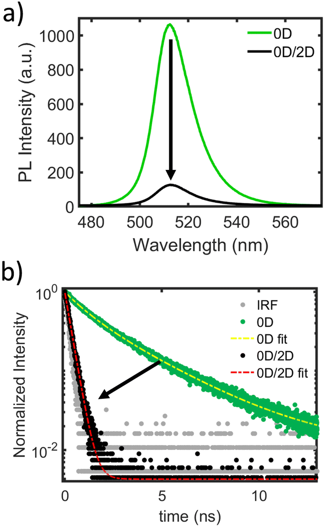 | ||
| Fig. 3 (a) PL spectra of CsPbBr3 nanocrystals (green) and the 0D/2D CsPbBr3/MoSe2 heterostructure (black) showing significant quenching due to energy transfer. (b) PL decay of CsPbBr3 nanocrystals (green) and the 0D/2D CsPbBr3/MoSe2 heterostructure (black) showing fast decay due the new energy transfer channel. The Instrument Response Function (IRF) is shown in gray, while the fitting curves for CsPbBr3 nanocrystals and 0D/2D CsPbBr3/MoSe2 heterostructure are shown as yellow and red dotted curves, respectively. | ||
The efficiency of an energy transfer from the donor can be estimated using eqn (1):74
 | (1) |
 | (2) |
A more quantitative approach for the estimation of the energy transfer efficiency can be obtained from the time-resolved PL spectroscopy of both donor and acceptor emissions. Due to an efficient competing process of energy transfer, the donor shows much faster PL decay in the presence of an acceptor. For example, faster PL decay of CsPbBr3 NCs can be observed in presence of acceptor 2D MoSe2 as shown in Fig. 3(b). The difference in the rates of decay of the donor gives the energy transfer rate (KET) as shown in eqn 3:13
 | (3) |
 | (4) |
Evaluating the charge transfer in 0D/2D heterostructures by optical PL spectroscopy of acceptor (2D) component
Another phenomenon that potentially shows PL quenching and PL lifetime changes is direct charge transfer across the interface.81Fig. 2(a) and (d) shows an example of hole transfer from excited ITO nanocrystals and 2D MoS2 which forms a type-II heterostructure.19,20 According to the reference frame, it can be referred to as electron or hole transfer, depending on the system of interest. A peculiarity of 2D TMDs is the possibility to measure photoluminescence as the recombination of excitons as well as trions at room temperature.2,19 This allows drawing conclusions of carrier concentration changes in the sample after interaction with a donor material, such as 0D nanocrystals.13,19,20,82 Therefore, the exciton-to-trion ratio is a powerful tool to quantify the precise amount of doping in the material system.13,19,20 Notably, in the cases in which a high density of free carriers is present in the 2D TMDs, the excitons can bind to the free carriers, creating the so-called trions.4,83–85 Experimental observation of such charged exciton was first reported by Kheng et al., in 1993 in a semiconductor quantum well system of CdTe-Cd1−xZnxTe.86,87 However, in that case, the several nanometer thick samples could only result in exciton binding energies of few meV and trion (or charged exciton) binding energy an order of magnitude lower.86,87 Therefore, low-temperature experiments were required to observe the emissions from such species.86 Given the atomically thin nature of the 2D TMDs, the effect of dielectric screening is low, resulting in large exciton binding/disassociation energy.1,2,4,88 Hence, the PL contribution in the 2D TMD from excitons and trions can be observed as well at room temperature and is characterized by the respective distinctive energies.4,13,19 A typical example PL spectrum of 2D MoS2 at room temperature with deconvoluted exciton and trion contribution is shown in Fig. 4(a). In fact, the carrier density in thermal equilibrium between exciton (nX), trion (nT), and free carrier density (ne), follows a Boltzmann distribution. Eqn (5) describes this equilibrium for low excitation densities, where mX, mT and me are relative masses of exciton, trion and free electron respectively, and EB is the trion binding energy.13,87,89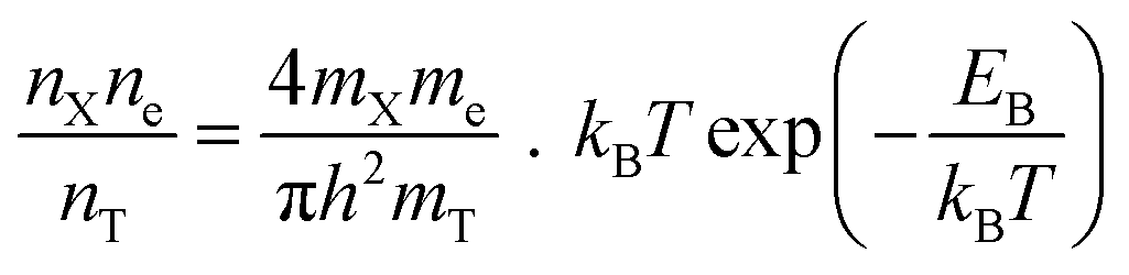 | (5) |
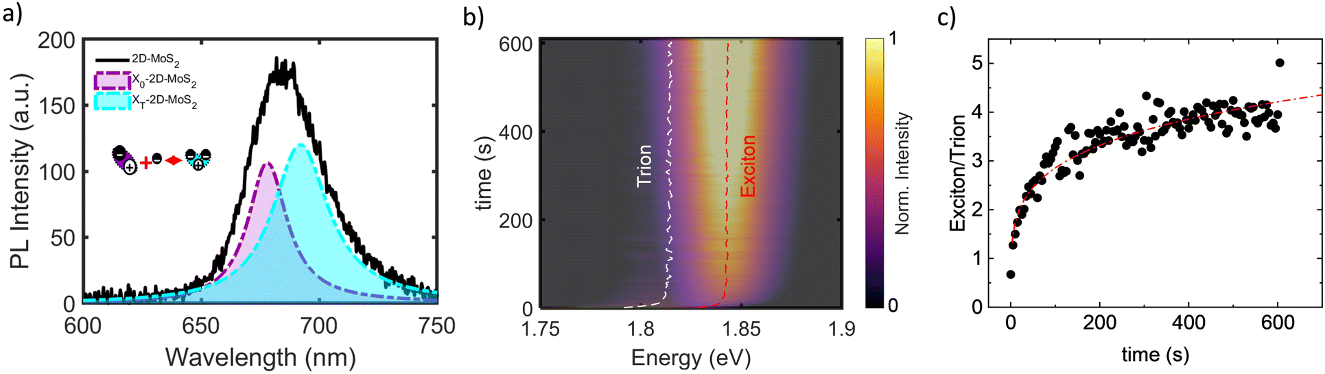 | ||
| Fig. 4 Temporal evolution of the spectrum of the 2D MoS2 PL in the 0D/2D hybrid nanosystem during photoinduced hole extraction. (a) PL spectrum of 2D MoS2 with deconvolution into exciton (purple Gaussian) and trion (light blue Gaussian). The inset depicts the schematics of the generation of a trion. (b) evolution of the PL spectra of the 2D MoS2 with the duration of photodoping. To guide the eye, the evolution of exciton and trion are depicted by red and white dashed lines, respectively. (c) Ratio of the intensity of the exciton to that of the trion.19 | ||
This equilibrium between the exciton, trion, and the free carrier density (see Fig. 4(a) inset) allows us to quantify the level of doping in the material system. For higher carrier densities and at low excitation fluences, the presence of trion PL is an indicator of the level of intrinsic doping with more intense trion PL for more free carriers.19,20,89 Similarly, for higher pump fluences with beyond bandgap photoexcitation, more trion PL is observed, as a result of an increased number of free carriers generated via photoexcitation.90–92 In several works, this correlation between the exciton-to-trion ratio and carrier density has been successfully employed to extract information on the level of doping or charge transfer.19,20 For example, the consequence of both n- and p-doping can be observed in the modulation of trion emission intensity and spectral shape using different dopants.93,94 The transfer of charges between layered 2D p-doped FePS3 and n-doped 2D MoS2 was also observed through room temperature steady-state PL spectroscopy of 2D MoS2.82
Evaluating the charge transfer in 0D/2D heterostructures by electrical transport measurements
The interface physics of 0D/2D heterostructures is complex and plays a crucial role in determining the optoelectronic properties of these heterostructures. One important consideration in evaluating the charge transfer in 0D/2D heterostructures is the fundamental differences in charge transport between 0D nanocrystals and 2D materials. In 2D materials, electrons are free to move only in two geometrical directions and are quantum mechanically confined in the third direction.95 This confinement leads to completely different electron emission behaviors in the in-plane and out-of-plane geometries, which must be taken into account when defining the emission mechanisms of 2D contacts and their heterostructures. Electrical transport measurements provide valuable insights into the charge transfer mechanisms in 0D/2D heterostructures. For example, the carrier lifetime, which can vary from 1 ps in monolayer 2D materials to 100 ps in multilayer structures, has a significant impact on the charge transfer dynamics.96,97 Intravalley and intervalley scattering processes can also influence the charge transfer by changing the center-of-mass momentum and phase of excitons, which are electron–hole pairs that play a crucial role in the radiative decay and emission of radiation.96 The combination of exciton dissociation and interfacial charge transfer determines the total response time of the heterostructures, which can be influenced by out-of-plane carrier drift and recombination of excitons.98 It is important to accurately measure and understand these parameters in order to evaluate the charge transfer mechanisms in 0D/2D heterostructures. Additionally, the role of interlayer coupling in light absorption and transport of photoexcited carriers is another important aspect that needs to be considered in the evaluation of charge transfer in these heterostructures. Experimental studies alone may not provide a complete understanding of the charge transport mechanisms and optoelectronic response in such heterostructures. Therefore, computational tools, such as first-principles density functional theory (DFT), can be utilized to predict the type of contact (Ohmic or Schottky) and estimate parameters such as barrier height, recombination, and defect density at the 2D-based contacts.99Charge transfer – the case of 0D/2D ITO/MoS2 heterostructure
Recent works reported the light-driven charge transfer of holes in a 0D/2D hybrid structure based on doped metal oxide (MO) NCs and 2D MoS2.19,20 The hybrid nanostructure of interest is composed of a single layer of 0D ITO-In2O3 core–shell nanocrystals deposited via spin-coating on top of a monolayer of MoS2. In this case, the charge transfer process of photogenerated holes is driven by the relative energetic band alignment between the two nanomaterials. As illustrated in Fig. 2(c), the 0D/2D hybrid forms of a staggered, type-II heterojunction. The coupling between the two materials enables the separation of photo-charges and hinders electron–hole recombination processes. The effects of the photoexcitation and the charge transfer can be monitored via PL spectroscopy. By selectively exciting only the 2D MoS2, it is possible to characterize the hybrid system without photoexciting the ITO nanocrystals. Before the photodoping process, 2D MoS2 is significantly n-doped as evidenced by the initial strong presence of trion and the low-energy PL. Subsequently, the evolution of the spectra were tracked vs. time of photodoping (Fig. 4(b)). The PL increases and shifts in energy (red dashed line for exciton and white dashed line for trion in Fig. 4(b)). Here, the reduction in n-type carriers in the 2D MoS2 caused by a charge transfer from the ITO nanocrystals is attributed to the hole transfer. Since the PL quantum yield of trions is lower than that of excitons, when more free electrons are removed, the relative spectral weight of the trion decreases while the exciton intensity increases.4,100 A significant reduction in the relative spectral weight of the trion and a corresponding increase in that of the exciton is observed, resulting in an increase of the exciton-to-trion ratio from ∼0.67 to ∼4.0 over the photodoping process (Fig. 4(c)). The increase in the exciton-to-trion ratio is assigned to a reduction in the density of negatively charged carriers in the 2D MoS2 due to photoinduced hole injection from the ITO nanocrystals. This is corroborated by the substantial blueshift of the energy of the exciton and trion (Fig. 5(a)), which follows nearly identical dynamics.19 Notably, the light-driven CT of holes is followed by the diffusion of the same charges in the 2D TMD up to 40 μm from the charge injection spot.20 The long-range diffusion of charges might play a major role supporting the permanent charge separation, if diffusion is faster than recombination.101–103 | ||
| Fig. 5 (a) Single particle (exciton) energy scheme showing energy transfer from CsPbBr3 nanocrystals to WS2 and (b) MoSe2 monolayers. (c) PL spectra showing enhancement of acceptor PL in CsPbBr3–WS2 heterostructure system. Reprinted with permission.15 Copyright The Royal Society of Chemistry 2018 and (d) PL spectra showing enhancement of acceptor PL in CsPbBr3–MoSe2 heterostructure system. | ||
Discussion – band-offset energy dependence
Further considerations to design the interaction between 0D and 2D materials are the band alignment of the 0D/2D heterostructures that includes the type, band-offsets’ energy etc. In the case of a single charge transfer from donor to acceptor and vice-versa, typically observed in type-II band alignment, the quenching of both donor and acceptor PL could be observed. Instead, in a type-I heterostructure or energy transfer system, it is expected to observe PL quenching of the 0D donor, in correlation with the enhancement of 2D acceptor PL. Given the above considerations, it is important to perform an in-depth study of the PL characteristics of the hybrid 0D/2D system in unison with an understanding of the 0D donor and the 2D acceptor system. This non-destructively tool combining the steady-state PL quenching (or enhancement), the PL life-time, but also the exciton-to-trion ratio in the 2D TMD PL, allows design in an optimized 0D/2D heterostructure. In the following, we provide specific examples of energy transfer affected by the band offsets. In principle, most of the reported work aims to improve the light absorption of 2D TMD via the addition of highly absorbing 0D materials, such as CdSe, halide perovskite NCs, etc.13,104 However, the transferred energy not always results in the enhancement of the emission of the acceptor.13,74 Depending on the bandgap of the donor, the transferred energy result in the excitation of the acceptor either close to exciton energy or at much higher energies in the exciton continuum (compare Fig. 5(a) and (b)). This is analogous with excitation energy dependent formation of excitons. For example, Trovatello et al. reported an ultrafast pump–probe spectroscopy study of excitation energy-dependent exciton formation in MoS2 monolayers.105 They show that with low-excitation energy, the exciton forms within 10 fs, and exciton formation time increases with increasing excitation energy.105 At very high excitation energies, Kozawa et al. reported that it is also possible for the electron and hole to separate in the momentum space and relax to the nearest local minima.106 Therefore, the bandgap offsets of the donor and acceptor play a crucial role in modifying the properties of the heterostructure in a 0D/2D system. Hence, in the case of exciton funneling to achieve an enhanced light emission from the acceptor, which is important for devices such as light-emitting diodes or NIR light sources, it is important to choose the donor with a bandgap comparable to the acceptor. However, this comes with the compromise that the spectral overlap which also influences the energy transfer efficiency might be lowered and consequently the efficiency. As an example, Liu et al. fabricated a 0D/2D heterostructure of CsPbBr3 nanocrystals (bandgap = 2.4 eV) and 2D WS2 (bandgap = 1.9 eV) and observed a photoinduced energy transfer from CsPbBr3 to 2D WS2 (see Fig. 5(a)). Upon the addition of CsPbBr3 nanocrystals on top of the 2D WS2, they recorded a faster PL decay of the nanocrystals and calculated the energy transfer rate and efficiency to be 2 × 10⁸ s−1 and 40%, respectively. The emission of 2D WS2 was enhanced 12 times with an internal quantum efficiency increase from 6 to 29%.107 For a similar 0D/2D CsPbBr3/WS2 system, Li et al., observed energy transfer that increased the exciton density by 69% and consequently the emission in the 2D WS2 layer (PL spectra of individual emission and heterostructure emission shown in Fig. 5(c)).15 On the other hand, when a similar CsPbBr3 nanocrystal was used together with 2D MoSe2 (bandgap = 1.55 eV), Asaithambi et al. show an efficient energy transfer from CsPbBr3 nanocrystals to the exciton continuum of 2D MoSe2 (see Fig. 5(b)).13 They calculated this photoinduced energy transfer efficiencies to be above 86% from the quenching of the donor PL. Instead, the enhancement of the PL in the MoSe2 remained at 33% only. By carefully analyzing the 2D MoSe2 PL, enhanced trion emission was found in the heterostructure, indicating the increase of free carriers in the 2D MoS2 layer, as discussed above (see Fig. 5(c)). Since the bandgap of CsPbBr3 is much larger compared to the 2D MoSe2, the energy transfer results into the exciton continuum and into the direct generation of free carriers out of which only 33% bind to form exciton and trion.13 A schematic illustration of the single particle energy diagram and energy transfer between 0D CsPbBr3 nanocrystals (donor) and WS2 on the one hand and MoSe2 on the other hand are shown in Fig. 5(a) and (b), respectively. It is illustrated the ground state together with the excited exciton and trion states, as well as the exciton continuum. In the case of energy transfer between 0D CsPbBr3 NCs and 2D WS2 the transferred energy is closer to the bound exciton level, resulting into a higher probability of exciton formation (Fig. 5(a)). On the contrary, in the case of 0D CsPbBr3 NCs and 2D MoSe2 the transferred energy results deep in the exciton continuum, with the effect of creating more free carriers and consequently more trion emission (Fig. 5(b) and (d)). Given the quantum well nature and the accommodation of the exciton complexes in the 2D TMD, the energy transfer from a 0D material alters the properties of the 2D TMD depending on the band-offset energy of the heterostructure. Hence, the band-offset becomes another parameter to design the heterostructure enabling dedicated PL enhancement (e.g. for light emitting applications) or enhanced free carrier density, beneficial where enhanced photocurrent is desired.Perspectives
Up to now we have been discussing the interaction mechanisms observed when coupling semiconducting nanocrystals to 2D TMDs and identified energy and charge transfer as the major interaction mechanisms. In the final part of this article, we will discuss opportunities arising by exploiting other materials parameters in the 0D as well as the 2D case. Beyond semiconductor NCs, integrating other nanoparticles with TMDs presents numerous exciting opportunities from both scientific and technological perspectives. For example, metallic NCs efficiently inject hot carriers into surrounding materials upon excitation of their localized surface plasmons,108–113 a property that has been exploited recently for localized chemical catalysis and light detection. This appealing strategy to achieve charge transfer in 0D/2D systems, even when the band alignment is not favorable, involves the generation of hot electrons. In plasmonic materials, the formation of hot electrons can be ignited by exciting plasmonic resonances, via non-radiative plasmon decay. These plasmonic hot electrons have been recently studied for photocatalysis,114 photodetection,115 the control of 2D material's transport properties,116 and solar energy applications.117,118 In particular, hot electrons are generated in solar cells or photodetectors through a process called plasmon-induced hot electron generation in the nanoparticle when illuminated with light. These energetic electrons can then be injected into the adjacent semiconductor, such as the photoactive layer of a solar cell or the active region of a photodetector.119,120Once injected into the semiconductor, hot electrons can contribute to the device's performance in several ways including enhanced photocurrent,121,122 reduced recombination losses,121 extended spectral response,121 and modified charge transport and recombination.123 Hot electron transfer processes have also been investigated in plasmonic nanostructures (e.g., NCs) for solar energy harvesting.88,124 The possibility of harvesting hot electrons via charge transfer is extremely appealing to overcome the current limitations of photovoltaic devices and increase solar cell's efficiency. Energy losses related to high-energy photons, whose excess energy with respect to the semiconductor's bandgap threshold is typically lost as heat, could be recovered via hot CT,124 while energy conversion processes in plasmonic solar cells would enormously benefit from efficient CT, limiting the energy losses related to ultrafast electron–electron scattering.88 Plasmonic hot electron transfer dynamics have been demonstrated in 0D/2D hybrid based on nanoparticles and MoS2 monolayers. For example, Li et al. reported the n-type doping of 2D MoS2 as a consequence of the charge transfer of hot electrons generated with resonating light in gold nanoparticles.88 More recently, Guizzardi et al. reported signatures of near-infrared plasmonic hot electron transfer in a 0D/2D hybrid composed of ITO NCs and 1L-MoS2via ultrafast differential transmission measurements.124 Owing to the extreme tunability of the localized surface plasmonic resonance of ITO NCs, heterojunctions based on MO NCs could be engineered for the harvesting of low energy photons in the near infrared regime, opening the way to the next-generation of infrared solar cells based on plasmon induced hot electron transfer.124 Furthermore, combining the electronic properties and small footprint of TMDs with the large optical cross-sections and geometry-tunable plasmon resonances of metallic NCs has the potential to fill the existing need for photodetectors in the short-wave infrared region of the spectrum (∼1–2.5 μm) where current detectors are both expensive and noisy. The large fields associated with plasmonic NCs can also greatly enhance direct light absorption and emission,125–130 as well as nonlinear frequency conversion,131–133 in atomically thin monolayers of TMDs, all of which is beneficial for compact and efficient nanophotonic devices. Such effects are now being pushed to the quantum regime, where strong coupling between TMD excitons and plasmonic NC-based nano- and pico-cavities leads to polaritonic states134–139 whose energies and localized quantum-optical properties can be widely tuned by both electrical and mechanical means.140–145 Further, the sharp apices and field enhancement properties of plasmonic NCs (e.g. nanocubes and nanostars) can create deterministically positioned single-photon emitters in TMDs,146–149 a key component of future nanophotonic and quantum optical circuitry. Implementing plasmonic NCs with chiral geometries additionally allows researchers to directly address excitons in specific valleys of the TMD bandstructure, opening new opportunities in nanoscale valley-tronic and valley-photonic applications.150 Novel properties and performance can also be realized by coupling the class of NCs known as upconverting nanoparticles (UCNPs) to TMDs. UCNPs are insulating nanoparticles doped with lanthanide (Ln) ions, which absorb multiple low-energy photons and emit higher energy light,151–154 doing so with efficiencies that are 5 to 8 orders of magnitude higher than the best two-photon dye molecules.155–158 Despite their many advantages, the brightness of UCNPs is ultimately limited by the long luminescent lifetimes of the Ln ions, typically ∼1 ms.159 However, by efficiently coupling UCNPs to TMDs, ET can occur from a Ln ion to the TMD at rates that are thousands of times faster than Ln emission rates,160,161 followed by fast PL emission by the TMD. Thus, the hybrid UCNP-TMD can emit many more photons per second than an isolated UCNP, and is limited only by the engineered UCNP-TMD ET rate and not the Ln radiative lifetime. This will be particularly beneficial for single-photon emitter applications where a UCNP containing a single Ln ion can be used for quantum light emission at technologically relevant rates.162,163 In another vein, new UCNPs that support the photon avalanching process have recently shown photoswitching capabilities.164,165 By coupling to nanoparticles such as these, carbon dots166,167 or other NCs supporting photomodulated behavior, active nanoscale photoswitchable functionality can now be added to TMD exciton emission, enabling new capabilities in van der Waals photonic circuits including neuromorphic computing and data storage. Another possibility is to explore NC hybridization with other 2D materials that possess unique characteristics. In recent years, ferroelectric and ferromagnetic 2D materials, such as CuInP2S6 (CIPS), NiPS3, CoPS3, etc., have been used to form heterostructures with other nanocrystals, such as ITO nanocrystals or perovskites, gaining significant attention due to their promising properties and potential applications in several fields.168,169 For example, their exceptional electrical properties and high surface area make them a suitable candidate for advancements in energy storage devices such as supercapacitors, where ferroelectric 2D materials offer an attractive alternative to conventional energy storage systems.170,171 Moreover, ferroelectric 2D materials hold significant potential for improving the performance of non-volatile memory devices, which can retain stored data even when the power is turned off. When combined with NPs with shape anisotropy the polarization dependent excitation might induce particular interaction with the ferroelectric material.172–174 Perspectively, hybrid NC-ferroelectric 2D materials could offer improved speed, reliability, and scalability compared to conventional memory technologies. Additionally, the flexibility and transparency of these materials may enable use in next-generation, flexible and transparent electronic devices, such as solar cells and displays.
Challenges
As our nascent understanding of 0D–2D material hybrids grows, key scientific and technological challenges are also emerging. For example, researchers are learning that directly transferring a TMD on top of another material or substrate is not sufficient to produce intimate contact,175 and that carefully controlling the coupling between NCs and TMDs will require assembly with sub-nm precision. Further, the development of new characterization methods, capable of collecting and correlating structural and optoelectronic properties with resolution down to the atomic scale is needed for properly studying these systems. Despite the exciting prospects, the use of 2D materials for energy and charge transfer applications also faces several challenges. For instance, scalability remains a significant concern, as the large-scale synthesis and integration into devices is a complex and challenging task. Additionally, the production of conductive NC films over 2D material, which might be necessary for optoelectronic applications requires conditions of NC treatment that are not interfering with the 2D material's performance.Overall, hybrid NC-2D materials hold significant promise for the future of energy and charge transfer technologies. Their unique properties, combined with their potential to form heterostructures with other nanocrystals offer exciting possibilities for advancements in these fields. Ongoing research and development are necessary to fully realize their potential and overcome the challenges associated with their use in practical applications.
Conflicts of interest
There are no conflicts to declare.Acknowledgements
A. A., N. K. T., M. G., N. C., and I. K. acknowledge the support of both European Union's Horizon 2020 European Research Council, under grant agreement no. 850875 (I. K.) (Light-DYNAMO), and European Union's Horizon 2020 Research and Innovation program under grant agreement no. 101017821 (I.K.) (LIGHT-CAP). P. J. S. gratefully acknowledges support from Programmable Quantum Materials, an Energy Frontier Research Center funded by the US Department of Energy, Office of Science, Basic Energy Sciences, under award DE-SC0019443.Notes and references
- Q. H. Wang, K. Kalantar-Zadeh, A. Kis, J. N. Coleman and M. S. Strano, Nat. Nanotechnol., 2012, 7, 699–712 CrossRef CAS PubMed.
- K. F. Mak, C. Lee, J. Hone, J. Shan and T. F. Heinz, Phys. Rev. Lett., 2010, 105(13), 136805 CrossRef PubMed.
- A. Splendiani, L. Sun, Y. Zhang, T. Li, J. Kim, C.-Y. Chim, G. Galli and F. Wang, Nano Lett., 2010, 10, 1271–1275 CrossRef CAS PubMed.
- K. F. Mak, K. He, C. Lee, G. H. Lee, J. Hone, T. F. Heinz and J. Shan, Nat. Mater., 2012, 12, 207–211 CrossRef PubMed.
- M. Velický, G. E. Donnelly, W. R. Hendren, S. McFarland, D. Scullion, W. J. I. DeBenedetti, G. C. Correa, Y. Han, A. J. Wain, M. A. Hines, D. A. Muller, K. S. Novoselov, H. D. Abruńa, R. M. Bowman, E. J. G. Santos and F. Huang, ACS Nano, 2018, 12, 10463–10472 CrossRef PubMed.
- G. Y. Jia, Y. Liu, J. Y. Gong, D. Y. Lei, D. L. Wang and Z. X. Huang, J. Mater. Chem. C, 2016, 4, 8822–8828 RSC.
- Y. Yu, Y. Zhang, X. Song, H. Zhang, M. Cao, Y. Che, H. Dai, J. Yang, H. Zhang and J. Yao, ACS Photonics, 2017, 4, 950–956 CrossRef CAS.
- D. Andrzejewski, H. Myja, M. Heuken, A. Grundmann, H. Kalisch, A. Vescan, T. Kümmell and G. Bacher, ACS Photonics, 2019, 6, 1832–1839 CrossRef CAS.
- D. Kufer and G. Konstantatos, ACS Photonics, 2016, 3, 2197–2210 CrossRef CAS.
- S. Ahmed and J. Yi DOI:10.1007/s40820-017-0152-6.
- Y. Cao, P. Qu, C. Wang, J. Zhou, M. Li, X. Yu, X. Yu, J. Pang, W. Zhou, H. Liu and G. Cuniberti, Adv. Opt. Mater., 2022, 10, 2200816 CrossRef CAS.
- D. Kufer and G. Konstantatos, ACS Photonics, 2016, 3, 2197–2210 CrossRef CAS.
- A. Asaithambi, N. K. Tofighi, N. Curreli, M. de Franco, A. Patra, N. Petrini, D. Baranov, L. Manna, F. di Stasio and I. Kriegel, Adv. Opt. Mater., 2022, 10, 2200638 CrossRef CAS.
- M. Ghini, N. Curreli, A. Camellini, M. Wang, A. Asaithambi and I. Kriegel, Nanoscale, 2021, 13, 8773–8783 RSC.
- H. Li, X. Zheng, Y. Liu, Z. Zhang and T. Jiang, Nanoscale, 2018, 10, 1650–1659 RSC.
- M. de Franco, M. Cirignano, T. Cavattoni, H. Bahmani Jalali, M. Prato and F. di Stasio, Opt. Mater.: X, 2022, 13, 100124 CAS.
- Y. Pu, F. Cai, D. Wang, J. X. Wang and J. F. Chen, Ind. Eng. Chem. Res., 2018, 57, 1790–1802 CrossRef CAS.
- Q. A. Akkerman, G. Rainò, M. V. Kovalenko and L. Manna, Nat. Mater., 2018, 17, 394–405 CrossRef CAS PubMed.
- I. Kriegel, M. Ghini, S. Bellani, K. Zhang, A. W. Jansons, B. M. Crockett, K. M. Koskela, E. S. Barnard, E. Penzo, J. E. Hutchison, J. A. Robinson, L. Manna, N. J. Borys and P. J. Schuck, J. Phys. Chem. C, 2020, 124, 8000–8007 CrossRef CAS.
- M. Ghini, E. S. Yanev, C. Kastl, K. Zhang, A. W. Jansons, B. M. Crockett, K. M. Koskela, E. S. Barnard, E. Penzo, J. E. Hutchison, J. A. Robinson, L. Manna, N. J. Borys, P. J. Schuck and I. Kriegel, Adv. Photonics Res., 2021, 2, 2000151 CrossRef.
- U. Woggon, Optical properties of semiconductor quantum dots, Springer, 1997, vol. 136 Search PubMed.
- J. G. Lu, Z. Z. Ye, Y. Z. Zhang, Q. L. Liang, S. Fujita and Z. L. Wang, Appl. Phys. Lett., 2006, 89, 023122 CrossRef.
- S. M. Cronenwett, T. H. Oosterkamp and L. P. Kouwenhoven, Science, 1998, 281, 540–544 CrossRef CAS PubMed.
- M. Makkar and R. Viswanatha, RSC Adv., 2018, 8, 22103–22112 RSC.
- A. di Carlo, A. Agresti, F. Brunetti and S. Pescetelli, J. Phys.: Energy, 2020, 2, 031003 CAS.
- C. Xie, C. K. Liu, H. L. Loi and F. Yan, Adv. Funct. Mater., 2020, 30, 1903907 CrossRef CAS.
- A. Boulesbaa, K. Wang, M. Mahjouri-Samani, M. Tian, A. A. Puretzky, I. Ivanov, C. M. Rouleau, K. Xiao, B. G. Sumpter and D. B. Geohegan, J. Am. Chem. Soc., 2016, 138, 14713–14719 CrossRef CAS PubMed.
- A. Raja, A. Montoya-Castillo, J. Zultak, X. X. Zhang, Z. Ye, C. Roquelet, D. A. Chenet, A. M. van der Zande, P. Huang, S. Jockusch, J. Hone, D. R. Reichman, L. E. Brus and T. F. Heinz, Nano Lett., 2016, 16, 2328–2333 CrossRef CAS PubMed.
- K. Vandewal, S. Albrecht, E. T. Hoke, K. R. Graham, J. Widmer, J. D. Douglas, M. Schubert, W. R. Mateker, J. T. Bloking, G. F. Burkhard, A. Sellinger, J. M. J. Fréchet, A. Amassian, M. K. Riede, M. D. McGehee, D. Neher and A. Salleo, Nat. Mater., 2013, 13, 63–68 CrossRef PubMed.
- J. Jortner, M. Bixon, T. Langenbacher and M. E. Michel-Beyerle, Proc. Natl. Acad. Sci. U. S. A., 1998, 95, 12759–12765 CrossRef CAS PubMed.
- C. Casiraghi, A. Hartschuh, E. Lidorikis, H. Qian, H. Harutyunyan, T. Gokus, K. S. Novoselov and A. C. Ferrari, Nano Lett., 2007, 7, 2711–2717 CrossRef CAS PubMed.
- C. Lee, H. Yan, L. E. Brus, T. F. Heinz, J. Hone and S. Ryu, ACS Nano, 2010, 4, 2695–2700 CrossRef CAS PubMed.
- H. Li, Q. Zhang, C. C. R. Yap, B. K. Tay, T. H. T. Edwin, A. Olivier and D. Baillargeat, Adv. Funct. Mater., 2012, 22, 1385–1390 CrossRef CAS.
- Y. Kim, J. G. Song, Y. J. Park, G. H. Ryu, S. J. Lee, J. S. Kim, P. J. Jeon, C. W. Lee, W. J. Woo, T. Choi, H. Jung, H. B. R. Lee, J. M. Myoung, S. Im, Z. Lee, J. H. Ahn, J. Park and H. Kim, Sci. Rep., 2016, 6, 1–8 CrossRef PubMed.
- Y. Niu, S. Gonzalez-Abad, R. Frisenda, P. Marauhn, M. Drüppel, P. Gant, R. Schmidt, N. S. Taghavi, D. Barcons, A. J. Molina-Mendoza, S. M. de Vasconcellos, R. Bratschitsch, D. P. de Lara, M. Rohlfing and A. Castellanos-Gomez, Nanomaterials, 2018, 8, 725 CrossRef PubMed.
- A. Steinhoff, J. H. Kim, F. Jahnke, M. Rösner, D. S. Kim, C. Lee, G. H. Han, M. S. Jeong, T. O. Wehling and C. Gies, Nano Lett., 2015, 15, 6841–6847 CrossRef CAS PubMed.
- O. I. Mićić, S. P. Ahrenkiel, D. Bertram and A. J. Nozik, Appl. Phys. Lett., 1999, 75, 478 CrossRef.
- Q. Li, C. Liu, Z. Liu, Q. Gong, Y. Hu, H. Rockel, S. R. Marder and J. W. Perry, Opt. Express, 2005, 13, 1833–1838 CrossRef CAS PubMed.
- H. Du, C. Chen, R. Krishnan, T. D. Krauss, J. M. Harbold, F. W. Wise, M. G. Thomas and J. Silcox, Nano Lett., 2002, 2, 1321–1324 CrossRef CAS.
- X. Zhao, I. Gorelikov, S. Musikhin, S. Cauchi, V. Sukhovatkin, E. H. Sargent and E. Kumacheva, Langmuir, 2005, 21, 1086–1090 CrossRef CAS PubMed.
- L. Qu and X. Peng, J. Am. Chem. Soc., 2002, 124, 2049–2055 CrossRef CAS PubMed.
- T. Mokari, M. Zhang and P. Yang, J. Am. Chem. Soc., 2007, 129, 9864–9865 CrossRef CAS PubMed.
- D. Zhu, F. Bellato, H. Bahmani Jalali, F. di Stasio, M. Prato, Y. P. Ivanov, G. Divitini, I. Infante, L. de Trizio and L. Manna, J. Am. Chem. Soc., 2022, 144, 10515–10523 CrossRef CAS PubMed.
- M. Imran, P. Ijaz, D. Baranov, L. Goldoni, U. Petralanda, Q. Akkerman, A. L. Abdelhady, M. Prato, P. Bianchini, I. Infante and L. Manna, Nano Lett., 2018, 18, 7822–7831 CrossRef CAS PubMed.
- I. Kriegel, F. Scotognella and L. Manna, Phys. Rep., 2017, 674, 1–52 CrossRef CAS.
- B. Lang, Surf. Sci., 1975, 53, 317–329 CrossRef CAS.
- K. S. Novoselov, D. Jiang, F. Schedin, T. J. Booth, V. V. Khotkevich, S. V. Morozov and A. K. Geim, Proc. Natl. Acad. Sci. U. S. A., 2005, 102, 10451–10453 CrossRef CAS PubMed.
- H.-W. Guo, Z. Hu, Z.-B. Liu, J.-G. Tian, H.-W. Guo, Z. Hu, Z.-B. Liu and J.-G. Tian, Adv. Funct. Mater., 2021, 31, 2007810 CrossRef CAS.
- F. Bonaccorso, A. Lombardo, T. Hasan, Z. Sun, L. Colombo and A. C. Ferrari, Mater. Today, 2012, 15, 564–589 CrossRef CAS.
- N. Wang, G. Yang, H. Wang, C. Yan, R. Sun and C. P. Wong, Mater. Today, 2019, 27, 33–42 CrossRef CAS.
- Z. Hu, Z. B. Liu and J. G. Tian, Chin. J. Chem., 2020, 38, 981–995 CrossRef CAS.
- X. Zhang, Y. Li, W. Mu, W. Bai, X. Sun, M. Zhao, Z. Zhang, F. Shan and Z. Yang, 2D Mater., 2021, 8, 032002 CrossRef CAS.
- Y. Huang, Y. H. Pan, R. Yang, L. H. Bao, L. Meng, H. L. Luo, Y. Q. Cai, G. D. Liu, W. J. Zhao, Z. Zhou, L. M. Wu, Z. L. Zhu, M. Huang, L. W. Liu, L. Liu, P. Cheng, K. H. Wu, S. B. Tian, C. Z. Gu, Y. G. Shi, Y. F. Guo, Z. G. Cheng, J. P. Hu, L. Zhao, G. H. Yang, E. Sutter, P. Sutter, Y. L. Wang, W. Ji, X. J. Zhou and H. J. Gao, Nat. Commun., 2020, 11, 1–9 CrossRef.
- F. Liu, W. Wu, Y. Bai, S. H. Chae, Q. Li, J. Wang, J. Hone and X. Y. Zhu, Science, 2020, 367, 903–906 CrossRef CAS PubMed.
- J. N. Coleman, M. Lotya, A. O’Neill, S. D. Bergin, P. J. King, U. Khan, K. Young, A. Gaucher, S. De, R. J. Smith, I. V. Shvets, S. K. Arora, G. Stanton, H. Y. Kim, K. Lee, G. T. Kim, G. S. Duesberg, T. Hallam, J. J. Boland, J. J. Wang, J. F. Donegan, J. C. Grunlan, G. Moriarty, A. Shmeliov, R. J. Nicholls, J. M. Perkins, E. M. Grieveson, K. Theuwissen, D. W. McComb, P. D. Nellist and V. Nicolosi, Science, 2011, 331, 568–571 CrossRef CAS PubMed.
- A. C. Ferrari, F. Bonaccorso, V. Fal’ko, K. S. Novoselov, S. Roche, P. Bøggild, S. Borini, F. H. L. Koppens, V. Palermo, N. Pugno, J. A. Garrido, R. Sordan, A. Bianco, L. Ballerini, M. Prato, E. Lidorikis, J. Kivioja, C. Marinelli, T. Ryhänen, A. Morpurgo, J. N. Coleman, V. Nicolosi, L. Colombo, A. Fert, M. Garcia-Hernandez, A. Bachtold, G. F. Schneider, F. Guinea, C. Dekker, M. Barbone, Z. Sun, C. Galiotis, A. N. Grigorenko, G. Konstantatos, A. Kis, M. Katsnelson, L. Vandersypen, A. Loiseau, V. Morandi, D. Neumaier, E. Treossi, V. Pellegrini, M. Polini, A. Tredicucci, G. M. Williams, B. Hee Hong, J. H. Ahn, J. Min Kim, H. Zirath, B. J. Van Wees, H. Van Der Zant, L. Occhipinti, A. Di Matteo, I. A. Kinloch, T. Seyller, E. Quesnel, X. Feng, K. Teo, N. Rupesinghe, P. Hakonen, S. R. T. Neil, Q. Tannock, T. Löfwander and J. Kinaret, Nanoscale, 2015, 7, 4598–4810 RSC.
- T. Kang, T. W. Tang, B. Pan, H. Liu, K. Zhang and Z. Luo, ACS Mater. Au, 2022, 2, 665–685 CrossRef CAS PubMed.
- F. Reale, P. Palczynski, I. Amit, G. F. Jones, J. D. Mehew, A. Bacon, N. Ni, P. C. Sherrell, S. Agnoli, M. F. Craciun, S. Russo and C. Mattevi, Sci. Rep., 2017, 7, 1–10 CrossRef CAS PubMed.
- J. Wang, T. Li, Q. Wang, W. Wang, R. Shi, N. Wang, A. Amini and C. Cheng, Mater. Today Adv., 2020, 8, 100098 CrossRef.
- S. Tajik, Z. Dourandish, F. Garkani Nejad, H. Beitollahi, P. M. Jahani and A. Di Bartolomeo, Biosens. Bioelectron., 2022, 216, 114674 CrossRef CAS PubMed.
- S. Mishra, Chem. Commun., 2022, 58, 10136–10153 RSC.
- B. Zhang, L. Goldoni, C. Lambruschini, L. Moni, M. Imran, A. Pianetti, V. Pinchetti, S. Brovelli, L. De Trizio and L. Manna, Nano Lett., 2020, 20, 8847–8853 CrossRef CAS PubMed.
- A. M. Negrescu, M. S. Killian, S. N. V. Raghu, P. Schmuki, A. Mazare and A. Cimpean, J. Funct. Biomater., 2022, 13, 274 CrossRef CAS PubMed.
- U. Kortshagen, J. Phys. D: Appl. Phys., 2009, 42, 113001 CrossRef.
- A. V. Nikam, B. L. V. Prasad and A. A. Kulkarni, CrystEngComm, 2018, 20, 5091–5107 RSC.
- V. Lesnyak, N. Gaponik and A. Eychmüller, Chem. Soc. Rev., 2013, 42, 2905–2929 RSC.
- M. de Franco, D. Zhu, A. Asaithambi, M. Prato, E. Charalampous, S. Christodoulou, I. Kriegel, L. de Trizio, L. Manna, H. Bahmani Jalali and F. di Stasio, ACS Energy Lett., 2022, 2022, 3788–3790 CrossRef PubMed.
- C. Bradac, Z. Q. Xu and I. Aharonovich, Nano Lett., 2021, 21, 1193–1204 CrossRef CAS PubMed.
- Z. Hu, X. Liu, P. L. Hernández-Martínez, S. Zhang, P. Gu, W. Du, W. Xu, H. V. Demir, H. Liu and Q. Xiong, InfoMat, 2022, 4, e12290 CAS.
- X. Song, X. Liu, D. Yu, C. Huo, J. Ji, X. Li, S. Zhang, Y. Zou, G. Zhu, Y. Wang, M. Wu, A. Xie and H. Zeng, ACS Appl. Mater. Interfaces, 2018, 10, 2801–2809 CrossRef CAS PubMed.
- C. Zhang, Y. Zhang, Z. Fang, Y. Chen, Z. Chen, H. He and H. Zhu, ACS Appl. Mater. Interfaces, 2021, 13, 41895–41903 CrossRef CAS PubMed.
- H. P. Komsa and A. v Krasheninnikov, Phys. Rev. B: Condens. Matter Mater. Phys., 2013, 88, 085318 CrossRef.
- M. Z. Bellus, M. Li, S. D. Lane, F. Ceballos, Q. Cui, X. C. Zeng and H. Zhao, Nanoscale Horiz., 2016, 2, 31–36 RSC.
- A. A. Lutich, G. Jiang, A. S. Susha, A. L. Rogach, F. D. Stefani and J. Feldmann, Nano Lett., 2009, 9, 2636–2640 CrossRef CAS PubMed.
- J. R. Lakowicz, Principles of Fluorescence Spectroscopy, 2006, pp.1–954 Search PubMed.
- M. H. Chiu, C. Zhang, H. W. Shiu, C. P. Chuu, C. H. Chen, C. Y. S. Chang, C. H. Chen, M. Y. Chou, C. K. Shih and L. J. Li, Nat. Commun., 2015, 6, 1–6 Search PubMed.
- Y. Altintas, N. B. Kiremitler, S. Genc, M. S. Onses and E. Mutlugün, J. Phys. D: Appl. Phys., 2018, 51, 065111 CrossRef.
- A. A. Hussain and A. R. Pal, J. Mater. Chem. C, 2017, 5, 1136–1148 RSC.
- L. Wu, C. Huang, B. P. Emery, A. C. Sedgwick, S. D. Bull, X. P. He, H. Tian, J. Yoon, J. L. Sessler and T. D. James, Chem. Soc. Rev., 2020, 49, 5110–5139 RSC.
- W. R. Algar, N. Hildebrandt, S. S. Vogel and I. L. Medintz, Nat. Methods, 2019, 16, 815–829 CrossRef CAS PubMed.
- C. Zhang, Y. Zhang, Z. Fang, Y. Chen, Z. Chen, H. He and H. Zhu, ACS Appl. Mater. Interfaces, 2021, 13, 41895–41903 CrossRef CAS PubMed.
- M. Ramos, F. Marques-Moros, D. L. Esteras, S. Mañ As-Valero, E. Henríquez-Guerra, M. Gadea, J. J. Baldoví, J. Canet-Ferrer, E. Coronado and M. R. Calvo, ACS Appl. Mater. Interfaces, 2022, 14, 33490 Search PubMed.
- J. Yang, T. Lü, Y. W. Myint, J. Pei, D. Macdonald, J. C. Zheng and Y. Lu, ACS Nano, 2015, 9, 6603–6609 CrossRef CAS PubMed.
- A. Arora, T. Deilmann, T. Reichenauer, J. Kern, S. Michaelis De Vasconcellos, M. Rohlfing and R. Bratschitsch, Phys. Rev. Lett., 2019, 123, 167401 CrossRef CAS PubMed.
- N. Lundt, E. Cherotchenko, O. Iff, X. Fan, Y. Shen, P. Bigenwald, A. V. Kavokin, S. Höfling and C. Schneider, Appl. Phys. Lett., 2018, 112, 031107 CrossRef.
- K. Kheng, R. T. Cox, Y. Merle D’aubigne, F. Bassani, K. Saminadayar and S. Tatarenko, Phys. Rev. Lett., 1993, 71(11), 1752 CrossRef CAS PubMed.
- J. Siviniant, D. Scalbert, A. V. Kavokin, D. Coquillat and J. P. Lascaray, Phys. Rev. B: Condens. Matter Mater. Phys., 1999, 59, 1602 CrossRef CAS.
- Z. Li, Y. Xiao, Y. Gong, Z. Wang, Y. Kang, S. Zu, P. M. Ajayan, P. Nordlander and Z. Fang, ACS Nano, 2015, 9, 10158–10164 CrossRef CAS PubMed.
- J. Duan, P. Chava, M. Ghorbani-Asl, D. Erb, L. Hu, A. V. Krasheninnikov, H. Schneider, L. Rebohle, A. Erbe, M. Helm, Y. J. Zeng, S. Zhou and S. Prucnal, Adv. Funct. Mater., 2021, 31, 2104960 CrossRef CAS.
- H. Yang, K. Wei, T. Jiang, X. Cheng and Y. Liu, Appl. Opt., 2016, 55, 6251–6255 CrossRef PubMed.
- A. O. A. Tanoh, J. Alexander-Webber, J. Xiao, G. Delport, C. A. Williams, H. Bretscher, N. Gauriot, J. Allardice, R. Pandya, Y. Fan, Z. Li, S. Vignolini, S. D. Stranks, S. Hofmann and A. Rao, Nano Lett., 2019, 19, 6299–6307 CrossRef CAS PubMed.
- A. Asaithambi, R. Kozubek, G. M. Prinz, F. Reale, E. Pollmann, M. Ney, C. Mattevi, M. Schleberger and A. Lorke, Phys. Status Solidi RRL, 2021, 15, 2000466 CrossRef CAS.
- S. Zhang, H. M. Hill, K. Moudgil, C. A. Richter, A. R. Hight Walker, S. Barlow, S. R. Marder, C. A. Hacker and S. J. Pookpanratana, Adv. Mater., 2018, 30(36), 1802991 CrossRef PubMed.
- Y. Wang, A. Slassi, M. A. Stoeckel, S. Bertolazzi, J. Cornil, D. Beljonne and P. Samorì, J. Phys. Chem. Lett., 2019, 10, 540–547 CrossRef CAS PubMed.
- Y. Li, S. Huang, S. Peng, H. Jia, J. Pang, B. Ibarlucea, C. Hou, Y. Cao, W. Zhou, H. Liu, G. Cuniberti, Y. Li, J. Pang, C. Hou, W. Zhou, H. Liu, S. Huang, G. Cuniberti, S. Peng, H. Jia and Y. Cao, Small, 2023, 19, 2206126 CrossRef CAS PubMed.
- D. B. Sulas-Kern, E. M. Miller and J. L. Blackburn, Energy Environ. Sci., 2020, 13, 2684–2740 RSC.
- Z. Hu, Z. Wu, C. Han, J. He, Z. Ni and W. Chen, Chem. Soc. Rev., 2018, 47, 3100–3128 RSC.
- D. Jariwala, V. K. Sangwan, L. J. Lauhon, T. J. Marks and M. C. Hersam, ACS Nano, 2014, 8, 1102–1120 CrossRef CAS PubMed.
- L. D. N. Mouafo, F. Godel, L. Simon, Y. J. Dappe, W. Baaziz, U. N. Noumbé, E. Lorchat, M. B. Martin, S. Berciaud, B. Doudin, O. Ersen, B. Dlubak, P. Seneor and J. F. Dayen, Adv. Funct. Mater., 2021, 31, 2008255 CrossRef CAS.
- J. S. Ross, S. Wu, H. Yu, N. J. Ghimire, A. M. Jones, G. Aivazian, J. Yan, D. G. Mandrus, D. Xiao, W. Yao and X. Xu, Nat. Commun., 2013, 4, 1–6 Search PubMed.
- Y. Liu, A. Elbanna, W. Gao, J. Pan, Z. Shen, J. Teng, Y. Liu, A. Elbanna, J. Pan, J. Teng, W. Gao and Z. Shen, Adv. Mater., 2022, 34, 2107138 CrossRef CAS PubMed.
- Z. Hu, X. Liu, P. L. Hernández-Martínez, S. Zhang, P. Gu, W. Du, W. Xu, H. V. Demir, H. Liu and Q. Xiong, InfoMat, 2022, 4, e12290 CAS.
- T. Zhu, L. Yuan, Y. Zhao, M. Zhou, Y. Wan, J. Mei and L. Huang, Sci. Adv., 2018, 4(1), 3104 CrossRef PubMed.
- N. Taghipour, P. L. H. Martinez, A. Ozden, M. Olutas, D. Dede, K. Gungor, O. Erdem, N. K. Perkgoz and H. V. Demir, ACS Nano, 2018, 12, 8547–8554 CrossRef CAS PubMed.
- C. Trovatello, F. Katsch, N. J. Borys, M. Selig, K. Yao, R. Borrego-Varillas, F. Scotognella, I. Kriegel, A. Yan, A. Zettl, P. J. Schuck, A. Knorr, G. Cerullo and S. D. Conte, Nat. Commun., 2020, 11, 1–8 CrossRef PubMed.
- D. Kozawa, R. Kumar, A. Carvalho, K. K. Amara, W. Zhao, S. Wang, M. Toh, R. M. Ribeiro, A. H. Castro Neto, K. Matsuda and G. Eda DOI:10.1038/ncomms5543.
- X. Fu, J. Qian, X. Qiao, P. E. Tan, Z. Peng, O. Lopez-Sanchez, D. Lembke, M. Kayci, A. Radenovic and A. N. Kis, Opt. Mater. Express, 2017, 7, 1327–1334 CrossRef.
- Y. Zhang, S. He, W. Guo, Y. Hu, J. Huang, J. R. Mulcahy and W. D. Wei, Chem. Rev., 2018, 118, 2927–2954 CrossRef CAS PubMed.
- H. Chalabi and M. L. Brongersma, Nat. Nanotechnol., 2013, 8, 229–230 CrossRef CAS PubMed.
- P. J. Schuck, Nat. Nanotechnol., 2013, 8, 799–800 CrossRef CAS PubMed.
- A. O. Govorov, H. Zhang and Y. K. Gun’Ko, J. Phys. Chem. C, 2013, 117, 16616–16631 CrossRef CAS.
- M. W. Knight, H. Sobhani, P. Nordlander and N. J. Halas, Science, 2011, 332, 702–704 CrossRef CAS PubMed.
- T. Hong, B. Chamlagain, S. Hu, S. M. Weiss, Z. Zhou and Y. Q. Xu, ACS Nano, 2015, 9, 5357–5363 CrossRef CAS PubMed.
- M. J. Kale, T. Avanesian and P. Christopher, ACS Catal., 2014, 4, 116–128 CrossRef CAS.
- X. Zhu, L. Shi, M. S. Schmidt, A. Boisen, O. Hansen, J. Zi, S. Xiao and N. A. Mortensen, Nano Lett., 2013, 13, 4690–4696 CrossRef CAS PubMed.
- Z. Fang, Z. Liu, Y. Wang, P. M. Ajayan, P. Nordlander and N. J. Halas, Nano Lett., 2012, 12, 3808–3813 CrossRef CAS PubMed.
- K. Wu, J. Chen, J. R. McBride and T. Lian, Science, 2015, 349, 632–635 CrossRef CAS PubMed.
- W. A. Tisdale, K. J. Williams, B. A. Timp, D. J. Norris, E. S. Aydil and X. Y. Zhu, Science, 2010, 328, 1543–1547 CrossRef CAS PubMed.
- H. Tang, C. J. Chen, Z. Huang, J. Bright, G. Meng, R. S. Liu and N. Wu, J. Chem. Phys., 2020, 152, 220901 CrossRef CAS PubMed.
- A. Furube and S. Hashimoto, NPG Asia Mater., 2017, 9, e454–e454 CrossRef CAS.
- T. Hong, B. Chamlagain, S. Hu, S. M. Weiss, Z. Zhou and Y. Q. Xu, ACS Nano, 2015, 9, 5357–5363 CrossRef CAS PubMed.
- T. Nakazawa, D. Kim, S. Kato, J. Park, J. Nam and H. Kim, Photonics, 2021, 8, 505 CrossRef CAS.
- C. G. Sánchez and M. Berdakin, J. Phys. Chem. C, 2022, 126, 10015–10023 CrossRef.
- M. Guizzardi, M. Ghini, A. Villa, L. Rebecchi, Q. Li, G. Mancini, F. Marangi, A. M. Ross, X. Zhu, I. Kriegel and F. Scotognella, J. Phys. Chem. Lett., 2022, 13, 11 Search PubMed.
- L. Novotny and B. Hecht, Principles of Nano-Optics, 2009, vol. 9781107005464, pp.1–564 Search PubMed.
- Y. Engineering, A. Zhang, Y. Wang, G. Long, Q. Chen, J. Li, J. Liu, Z. Guo, Z. Chang and Y. Guo, Molecules, 2022, 27, 2807 CrossRef PubMed.
- G. M. Akselrod, T. Ming, C. Argyropoulos, T. B. Hoang, Y. Lin, X. Ling, D. R. Smith, J. Kong and M. H. Mikkelsen, Nano Lett., 2015, 15, 3578–3584 CrossRef CAS PubMed.
- S. Butun, S. Tongay and K. Aydin, Nano Lett., 2015, 15, 2700–2704 CrossRef CAS PubMed.
- W. Bao, N. J. Borys, C. Ko, J. Suh, W. Fan, A. Thron, Y. Zhang, A. Buyanin, J. Zhang, S. Cabrini, P. D. Ashby, A. Weber-Bargioni, S. Tongay, S. Aloni, D. F. Ogletree, J. Wu, M. B. Salmeron and P. J. Schuck, Nat. Commun., 2015, 6, 1–7 Search PubMed.
- K. D. Park, T. Jiang, G. Clark, X. Xu and M. B. Raschke, Nat. Nanotechnol., 2017, 13, 59–64 CrossRef PubMed.
- K. D. Park and M. B. Raschke, Nano Lett., 2018, 18, 2912–2917 CrossRef CAS PubMed.
- Y. Li, M. Kang, J. Shi, K. Wu, S. Zhang and H. Xu, Nano Lett., 2017, 17, 7803–7808 CrossRef CAS PubMed.
- K. Yao, S. Zhang, E. Yanev, K. McCreary, H. J. Chuang, M. R. Rosenberger, T. Darlington, A. Krayev, B. T. Jonker, J. C. Hone, D. N. Basov and P. J. Schuck, Adv. Opt. Mater., 2022, 10, 2200085 CrossRef CAS.
- D. N. Basov, A. Asenjo-Garcia, P. J. Schuck, X. Zhu and A. Rubio, Nanophotonics, 2020, 10, 549–577 Search PubMed.
- D. G. Baranov, M. Wersäll, J. Cuadra, T. J. Antosiewicz and T. Shegai, ACS Photonics, 2018, 5, 24–42 CrossRef CAS.
- J. J. Baumberg, J. Aizpurua, M. H. Mikkelsen and D. R. Smith, Nat. Mater., 2019, 18, 668–678 CrossRef CAS PubMed.
- M. E. Kleemann, R. Chikkaraddy, E. M. Alexeev, D. Kos, C. Carnegie, W. Deacon, A. C. de Pury, C. Große, B. de Nijs, J. Mertens, A. I. Tartakovskii and J. J. Baumberg, Nat. Commun., 2017, 8, 1–7 CrossRef CAS PubMed.
- W. Liu, B. Lee, C. H. Naylor, H. S. Ee, J. Park, A. T. C. Johnson and R. Agarwal, Nano Lett., 2016, 16, 1262–1269 CrossRef CAS PubMed.
- T. Tufarelli, D. Friedrich, H. Groß, J. Hamm, O. Hess and B. Hecht, Phys. Rev. Res., 2021, 3, 033103 CrossRef CAS.
- T. P. Darlington, C. Carmesin, M. Florian, E. Yanev, O. Ajayi, J. Ardelean, D. A. Rhodes, A. Ghiotto, A. Krayev, K. Watanabe, T. Taniguchi, J. W. Kysar, A. N. Pasupathy, J. C. Hone, F. Jahnke, N. J. Borys and P. J. Schuck, Nat. Nanotechnol., 2020, 15, 854–860 CrossRef CAS PubMed.
- F. Dirnberger, J. D. Ziegler, P. E. Faria Junior, R. Bushati, T. Taniguchi, K. Watanabe, J. Fabian, D. Bougeard, A. Chernikov and V. M. Menon, Sci. Adv., 2021, 7, 3066–3095 CrossRef PubMed.
- D. Unuchek, A. Ciarrocchi, A. Avsar, K. Watanabe, T. Taniguchi and A. Kis, Nature, 2018, 560, 340–344 CrossRef CAS PubMed.
- N. R. Finney, M. Yankowitz, L. Muraleetharan, K. Watanabe, T. Taniguchi, C. R. Dean and J. Hone, Nat. Nanotechnol., 2019, 14, 1029–1034 CrossRef CAS PubMed.
- K. Yao, N. R. Finney, J. Zhang, S. L. Moore, L. Xian, N. Tancogne-Dejean, F. Liu, J. Ardelean, X. Xu, D. Halbertal, K. Watanabe, T. Taniguchi, H. Ochoa, A. Asenjo-Garcia, X. Zhu, D. N. Basov, A. Rubio, C. R. Dean, J. Hone and P. J. Schuck, Sci. Adv., 2021, 7(10), 8691 CrossRef PubMed.
- J. S. Ross, P. Klement, A. M. Jones, N. J. Ghimire, J. Yan, D. G. Mandrus, T. Taniguchi, K. Watanabe, K. Kitamura, W. Yao, D. H. Cobden and X. Xu, Nat. Nanotechnol., 2014, 9, 268–272 CrossRef CAS PubMed.
- A. Branny, S. Kumar, R. Proux and B. D. Gerardot, Nat. Commun., 2017, 8, 1–7 CrossRef PubMed.
- L. Peng, H. Chan, P. Choo, T. W. Odom, S. K. R. S. Sankaranarayanan and X. Ma, Nano Lett., 2020, 20, 5866–5872 CrossRef CAS PubMed.
- Y. Luo, G. D. Shepard, J. V. Ardelean, D. A. Rhodes, B. Kim, K. Barmak, J. C. Hone and S. Strauf, Nat. Nanotechnol., 2018, 13, 1137–1142 CrossRef CAS PubMed.
- J. Kern, I. Niehues, P. Tonndorf, R. Schmidt, D. Wigger, R. Schneider, T. Stiehm, S. Michaelis de Vasconcellos, D. E. Reiter, T. Kuhn, R. Bratschitsch, J. Kern, I. Niehues, P. Tonndorf, R. Schmidt, R. Schneider, T. Stiehm, S. Michaelis de Vasconcellos, R. Bratschitsch, D. Wigger, D. E. Reiter and T. Kuhn, Adv. Mater., 2016, 28, 7101–7105 CrossRef CAS PubMed.
- S. A. Vitale, D. Nezich, J. O. Varghese, P. Kim, N. Gedik, P. Jarillo-Herrero, D. Xiao, M. S. Rothschild, A. Vitale, D. Nezich, J. O. Varghese, M. Rothschild, P. Kim, N. Gedik, P. Jarillo-Herrero and D. Xiao, Small, 2018, 14, 1801483 CrossRef PubMed.
- E. M. Chan, E. S. Levy, B. E. Cohen, E. M. Chan, E. S. Levy and B. E. Cohen, Adv. Mater., 2015, 27, 5753–5761 CrossRef CAS PubMed.
- F. Auzel, Chem. Rev., 2004, 104, 139–173 CrossRef CAS PubMed.
- S. Wen, J. Zhou, K. Zheng, A. Bednarkiewicz, X. Liu and D. Jin, Nat. Commun., 2018, 9, 1–12 CrossRef CAS PubMed.
- F. Wang and X. Liu, Chem. Soc. Rev., 2009, 38, 976–989 RSC.
- S. Wu, G. Han, D. J. Milliron, S. Aloni, V. Altoe, D. V. Talapin, B. E. Cohen and P. J. Schuck, Proc. Natl. Acad. Sci. U. S. A., 2009, 106, 10917–10921 CrossRef CAS PubMed.
- Y. il Park, J. H. Kim, K. T. Lee, K. S. Jeon, H. bin Na, J. H. Yu, H. M. Kim, N. Lee, S. H. Choi, S. il Baik, H. Kim, S. P. Park, B. J. Park, Y. W. Kim, S. H. Lee, S. Y. Yoon, I. C. Song, W. K. Moon, Y. D. Suh and T. Hyeon, Adv. Mater., 2009, 21, 4467–4471 CrossRef.
- J. Zhao, D. Jin, E. P. Schartner, Y. Lu, Y. Liu, A. V. Zvyagin, L. Zhang, J. M. Dawes, P. Xi, J. A. Piper, E. M. Goldys and T. M. Monro, Nat. Nanotechnol., 2013, 8, 729–734 CrossRef CAS PubMed.
- D. J. Gargas, E. M. Chan, A. D. Ostrowski, S. Aloni, M. V. P. Altoe, E. S. Barnard, B. Sanii, J. J. Urban, D. J. Milliron, B. E. Cohen and P. J. Schuck, Nat. Nanotechnol., 2014, 9, 300–305 CrossRef CAS PubMed.
- E. M. Chan, E. S. Levy, B. E. Cohen, E. M. Chan, E. S. Levy and B. E. Cohen, Adv. Mater., 2015, 27, 5753–5761 CrossRef CAS PubMed.
- S. Wen, J. Zhou, P. J. Schuck, Y. D. Suh, T. W. Schmidt and D. Jin, Nat. Photonics, 2019, 13, 828–838 CrossRef CAS.
- A. Teitelboim, B. Tian, D. J. Garfield, A. Fernandez-Bravo, A. C. Gotlin, P. J. Schuck, B. E. Cohen and E. M. Chan, J. Phys. Chem. C, 2019, 123, 2678–2689 CrossRef CAS.
- Z. Sharifi, M. Dobinson, G. Hajisalem, M. S. Shariatdoust, A. L. Frencken, F. C. J. M. van Veggel and R. Gordon, J. Chem. Phys., 2021, 154, 184204 CrossRef CAS PubMed.
- A. Alizadehkhaledi, A. L. Frencken, M. K. Dezfouli, S. Hughes, F. C. J. M. van Veggel and R. Gordon, ACS Photonics, 2019, 6, 1125–1131 CrossRef CAS.
- C. Lee, E. Z. Xu, K. W. C. Kwock, A. Teitelboim, Y. Liu, N. Fardian-Melamed, C. C. S. Pedroso, H. S. Park, J. Kim, S. D. Pritzl, S. H. Nam, T. Lohmueller, P. Ercius, Y. D. Suh, B. E. Cohen, E. M. Chan and P. J. Schuck DOI:10.48550/arxiv.2209.06098.
- C. Lee, E. Z. Xu, Y. Liu, A. Teitelboim, K. Yao, A. Fernandez-Bravo, A. M. Kotulska, S. H. Nam, Y. D. Suh, A. Bednarkiewicz, B. E. Cohen, E. M. Chan and P. J. Schuck, Nature, 2021, 589, 230–235 CrossRef CAS PubMed.
- Y. P. Sun, B. Zhou, Y. Lin, W. Wang, K. A. S. Fernando, P. Pathak, M. J. Meziani, B. A. Harruff, X. Wang, H. Wang, P. G. Luo, H. Yang, M. E. Kose, B. Chen, L. M. Veca and S. Y. Xie, J. Am. Chem. Soc., 2006, 128, 7756–7757 CrossRef CAS PubMed.
- S. N. Baker, G. A. Baker, S. N. Baker and G. A. Baker, Angew. Chem., Int. Ed., 2010, 49, 6726–6744 CrossRef CAS PubMed.
- M. Liu, T. Liao, Z. Sun, Y. Gu and L. Kou, Phys. Chem. Chem. Phys., 2021, 23, 21376–21384 RSC.
- C. Cui, F. Xue, W. J. Hu and L. J. Li, npj 2D Mater. Appl., 2018, 2, 1–14 CrossRef.
- M. Hao Lee, W. Wu, M. H. Lee and W. Wu, Adv. Mater. Technol., 2022, 7, 2101623 CrossRef.
- X. K. Wei, N. Domingo, Y. Sun, N. Balke, R. E. Dunin-Borkowski and J. Mayer, Adv. Energy Mater., 2022, 12, 2201199 CrossRef CAS.
- H. C. Lu, N. Katyal, G. Henkelman and D. J. Milliron, J. Am. Chem. Soc., 2021, 143, 15745–15755 CrossRef CAS PubMed.
- S. Heo, S. H. Cho, C. J. Dahlman, A. Agrawal and D. J. Milliron, ACS Energy Lett., 2020, 5, 2662–2670 CrossRef CAS.
- J. Kim, A. Agrawal, F. Krieg, A. Bergerud and D. J. Milliron, Nano Lett., 2016, 16, 3879–3884 CrossRef CAS PubMed.
- K. Jo, P. Kumar, J. Orr, S. B. Anantharaman, J. Miao, M. J. Motala, A. Bandyopadhyay, K. Kisslinger, C. Muratore, V. B. Shenoy, E. A. Stach, N. R. Glavin and D. Jariwala, ACS Nano, 2021, 15, 5618–5630 CrossRef CAS PubMed.
| This journal is © The Royal Society of Chemistry 2023 |