
 Open Access Article
 This Open Access Article is licensed under a
 Creative Commons Attribution 3.0 Unported Licence
Self-assembled monolayer functionalized NiO nanowires: strategy to enhance the sensing performance of p-type metal oxide†
Navpreet
Kaur
 *a,
Mandeep
Singh
*ab,
Andrea
Casotto
cd,
Luigi
Sangaletti
c and
Elisabetta
Comini
a
*a,
Mandeep
Singh
*ab,
Andrea
Casotto
cd,
Luigi
Sangaletti
c and
Elisabetta
Comini
a
aSENSOR Laboratory, University of Brescia and INSTM UdR Brescia, Via D. Valotti 9, Brescia 25133, Italy. E-mail: n.kaur001@unibs.it; mandeep.singh@unibs.it
bDepartment of Physics, Politecnico Di Milano, Milano 20133, Italy
cI-LAMP and Dipartimento di Matematica e Fisica, Università Cattolica del Sacro Cuore, via della Garzetta 48, Brescia 25133, Italy
dDepartment of Chemistry and Biochemistry, University of Notre Dame, Notre Dame, IN 46556, USA
First published on 10th January 2023
Abstract
A novel strategy for the improvement in the sensing performance of p-type NiO is developed by employing the unique functional properties of self-assembled monolayers. Specifically, hole concentration near the surface of NiO nanowires (NWs) is modulated by terminal epoxy groups of the organosilane. This modulation leads to the increase in electron transfer from reducing gases to NWs surface. As a result, SAM-functionalized sensors showed 9-times higher response at low-temperature as compared to bare NiO NWs.
The development of high-performance p-type metal oxides (MOXs) based conductometric chemical sensors is still a huge challenge due to their unfavorable electrical properties.1 Specifically, the chemisorption of oxygen ions on their surface leads to the formation of a narrow conductive hole-accumulation layer (HAL)-shell around the highly resistive core (core–shell structure).2 Consequently, the charge carrier (hole in p-type MOXs) transport occurs within the narrow HAL leading to their highly resistive behavior.1 Thus, when p-type metal oxides are used as an active sensing layer, their response i.e. the change in their electric resistance/conductance, is quite low upon interaction with the gas analyte.1 In order to improve their electrical conductivity, consequently to achieve a high response to the particular gas analyte, generally p-type MOXs are operated at high temperatures (300–500 °C).3–6 However, the high-temperature operation leads to high power consumption hindering the commercialization of p-type MOX. Thus, achieving high performances for p-type MOX sensors at temperatures <300 °C remains a huge challenge. In this regard, researchers working in the field are trying different strategies to enhance the performance of p-type MOX sensors.1,7–11
Herein, we are proposing an alternative novel strategy based on the surface functionalization of p-type MOX (nickel oxide, NiO) with self-assembled monolayers (SAMs). SAMs are highly ordered molecular arrangements that form spontaneously on a variety of surfaces12 making them useful for various application areas such as biosensors,13 gas sensors,14 organic field effect transistors,15 nanoscale patterning, etc.16 Therefore the functionalization with SAMs can further widen the application of p-type MOX. In fact, SAM functionalization strategy has never been explored before in p-type MOX based gas sensors, according to the best of our knowledge. In this work, NiO NWs were functionalized with organosilane monolayer 3-glycidoxypropyltrimethoxysilane (GLYMO or GOPS) and explored for the detection of reducing gases. Our main goal is to modulate the surface charge carrier concentration via SAM terminal-groups for the achievement of optimised sensing performances (in terms of higher response at lower temperatures) towards reducing gases (acetone and ethanol). The experimental detail of NWs growth, functionaoization, sensor fabrication and characterization are provided in ESI.†
NiO NWs exhibit dense morphology (Fig. S4a and b, ESI†) with a highly crystalline bunsenite structure (Fig. S4c, ESI†). Raman spectra of NiO NWs is also presented in ESI† (Fig. S1d). While the observance of Si 2p peak in functionalized NWs (absent in bare NWs) confirms their successful surface functionalization with GOPS (Fig. S5, ESI†). Furthermore, in bare NiO NWs, the Ni![[thin space (1/6-em)]](https://www.rsc.org/images/entities/char_2009.gif) :O ratio was found between 0.6 to 0.7 (deviation from 1:1 stoichiometry) is attributed to the surface defects in NWs. While, in GOPS functionalized NWs, the quenching of Ni signal occurs due to the presence of GOPS monolayer on NWs surface. In fact, oxygen amounts in functionalized NWs also include the contribution of GOPS molecular structure (Table S1, ESI†). Further in-depth analysis reveals that the Ni 2p peak contains five components (Fig. 1a and e), out of which A belongs to Ni 2p3/2 spin–orbit component (BE: 854.1 eV) and it has an energy separation of 17.5 eV from the Ni 2p1/2 component (D).17,18 A more detailed analysis of the local, nonlocal, and charge transfer effects goes beyond the scope of this work. The O 1s core level spectra (Fig. 1c and g) of bare NiO NWs contains two components i.e. at BE = 530.1 eV (Ni–O bonds in bulk structure) and at BE = 532.1 eV (surface oxygen atoms). While in functionalized samples additional 3rd component at BE = 532.5 eV belongs to C–O bonds of GOPS is observed. On the hand, the shape of C 1s peak (Fig. 1b and f) was found to be different from bare NWs due to higher presence of C–O bond in SAM molecular structure. In addition to C–C (BE = 284.8 eV), C–O (BE = 286.0 eV) and C
:O ratio was found between 0.6 to 0.7 (deviation from 1:1 stoichiometry) is attributed to the surface defects in NWs. While, in GOPS functionalized NWs, the quenching of Ni signal occurs due to the presence of GOPS monolayer on NWs surface. In fact, oxygen amounts in functionalized NWs also include the contribution of GOPS molecular structure (Table S1, ESI†). Further in-depth analysis reveals that the Ni 2p peak contains five components (Fig. 1a and e), out of which A belongs to Ni 2p3/2 spin–orbit component (BE: 854.1 eV) and it has an energy separation of 17.5 eV from the Ni 2p1/2 component (D).17,18 A more detailed analysis of the local, nonlocal, and charge transfer effects goes beyond the scope of this work. The O 1s core level spectra (Fig. 1c and g) of bare NiO NWs contains two components i.e. at BE = 530.1 eV (Ni–O bonds in bulk structure) and at BE = 532.1 eV (surface oxygen atoms). While in functionalized samples additional 3rd component at BE = 532.5 eV belongs to C–O bonds of GOPS is observed. On the hand, the shape of C 1s peak (Fig. 1b and f) was found to be different from bare NWs due to higher presence of C–O bond in SAM molecular structure. In addition to C–C (BE = 284.8 eV), C–O (BE = 286.0 eV) and C![[double bond, length as m-dash]](https://www.rsc.org/images/entities/char_e001.gif) O (BE = 288.5 eV),14,19 peak belong to Si–C bond at BE = 283.1 eV is observed in GOPS-functioanlzied NWs. Finally, Si 2p peak (Fig. 1d and h) is only observed in functionalized samples that contains two components: at 103.0 eV (Si atoms in GOPS) and at 103.8 eV which attributed to the formation of silane species with four Si–O bonds.20
O (BE = 288.5 eV),14,19 peak belong to Si–C bond at BE = 283.1 eV is observed in GOPS-functioanlzied NWs. Finally, Si 2p peak (Fig. 1d and h) is only observed in functionalized samples that contains two components: at 103.0 eV (Si atoms in GOPS) and at 103.8 eV which attributed to the formation of silane species with four Si–O bonds.20
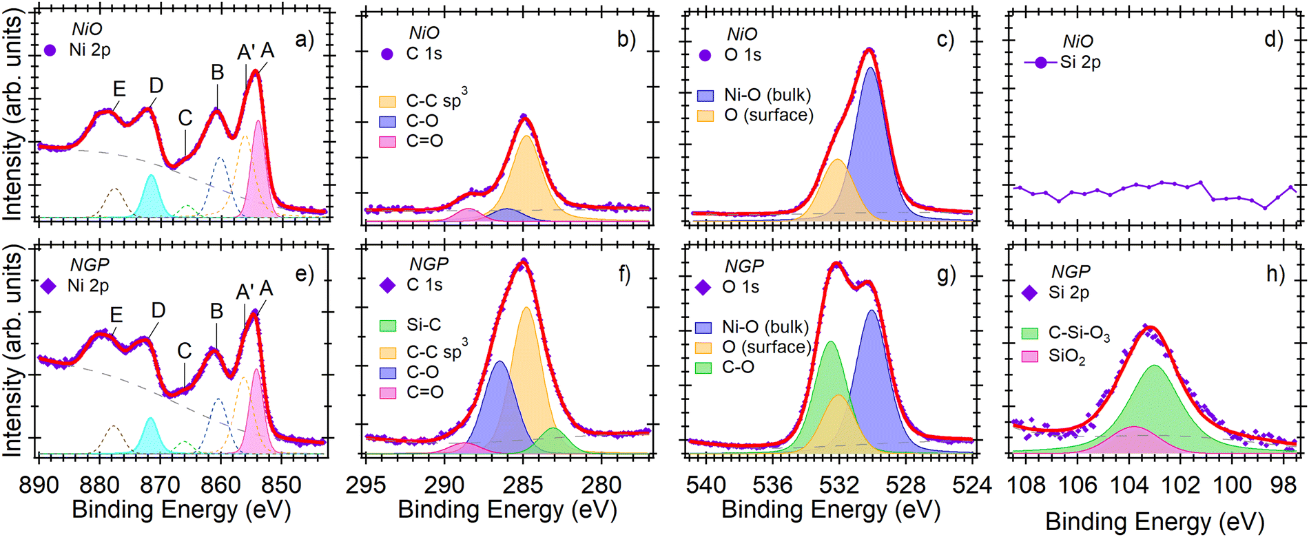 | ||
| Fig. 1 XPS core level spectra of the principal elements. The two columns are referred to the bare NiO and NGP samples, respectively. In each row, a specific energy region is showed: Ni 2p (a and e), C 1s (b and f), O 1s (c and g), and Si 2p (d and h). Violet markers denote the experimental trace, the red line is the total fit, and the dashed line represents the background. The Voigt peaks are included under each spectrum, along with their physical interpretation. The signals found in the Ni 2p region are discussed in the main text. | ||
Furthermore, the gas sensing performances of NGP sensors were tested towards different gas analytes such as H2, acetone, ethanol, methane (50 ppm), NO2 (5 ppm), NH3 (20 ppm) to investigate the sensors selectivity at 200 °C. The response values were determined from eqn. (S1) and (S2) (see ESI†). From Fig. 2a it is clearly observed that the NGP shows higher selectivity towards acetone and ethanol comparing to other compounds. Fig. 2(b and c) reports the isothermal dynamic-transient responses of NiO and NGP NWs toward the different concentrations of ethanol and acetone (10, 10, 20, 50, and 75 ppm) respectively at 200 °C in dry air. Evidently, for both the sensors, a decrease in sensor conductance was observed after the interaction with reducing gases. This confirms the p-type character of both NiO and NGP sensors.3 Specifically, when p-type MOXs like NiO are exposed to reducing gases, the donation of electrons from a gas analyte to the semiconductor surface leads to electron-hole recombination (holes are the majority charge carrier in NiO).3 This recombination causes a decrease in the hole concentration, hence decreasing the sensor conductance. Interestingly, the baseline conductance of the sensor was found to decrease after the GOPS functionalization, indicating the modulation in the charge carrier transport in nanowires. As the major focus of this work was to improve the sensing response at low temperatures, the responses of NiO and NGP toward ethanol and acetone were compared in Fig. 2(d and e) at 200 °C and 150 °C respectively. Evidently, NGP always exhibit higher responde as compared to bare NiO NWs at both temperatures. Indeed, for 75 ppm of ethanol and acetone, the NGP sensor exhibited 8- and 9-time higher response, respectively, in comparison to bare NiO NWs at 200 °C (other response values are provided in Table S2, ESI†). Furthermore, Fig. 2f reports the calibration curves (response vs. concentration), for NGP (200 °C and 150 °C) and NiO (200 °C). Considering the minimum response of 1, the detection limit of NGP was found to be 0.9 and 2 ppm at 200 °C towards ethanol and acetone respectively. The calculated coefficients and detection limits obtained from power fitting of curves (Fig. 2f) using eqn (S3) are provided in Table S3 (ESI†). Furthermore, the response/recovery times (Fig. S7, ESI†), response under humidity (Fig. S8a), stability (Fig. S8b), comparison with literature (Section 1.11) of NGP sensors are presented in ESI.†
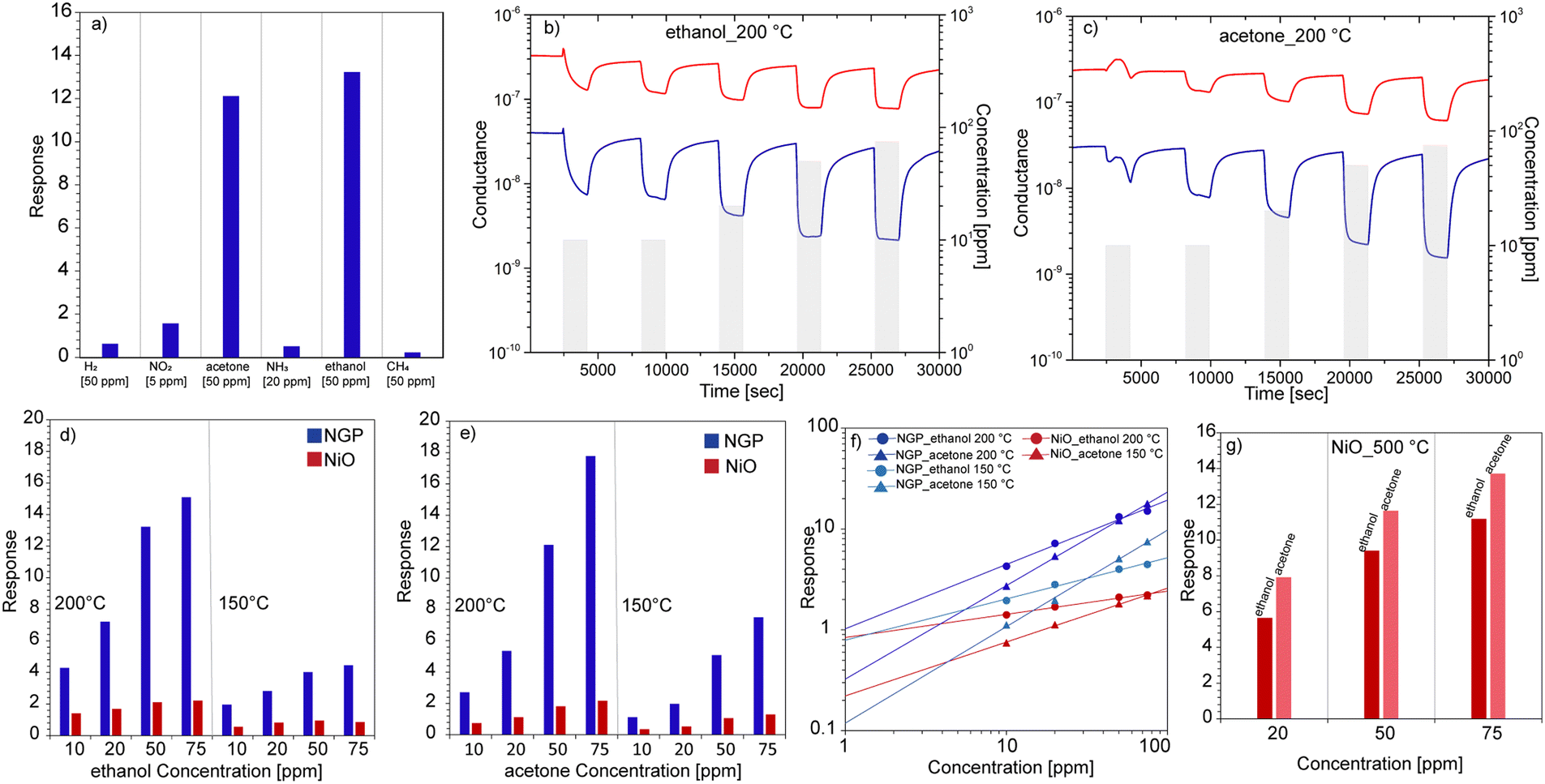 | ||
| Fig. 2 (a) Response (see eqn (S1) in ESI†) of NGP sensor toward different gas analytes. (b and c) Dynamic response of NiO (red) and NGP (blue) sensors toward the different concentrations of ethanol and acetone (10, 10, 20, 50, 75 ppm) in dry air at 200 °C. (d and e) Response vs. concentration curves of bare NiO and NGP at 200 °C and 150 °C toward ethanol and acetone. (f) Calibration curves of NiO and NGP sensors for ethanol and acetone. (g) Response vs. concentration graph of NiO sensor toward ethanol and acetone at 500 °C. | ||
Fig. 2g shows response values for bare NiO NWs: 11.2 and 13.7 at 500 °C towards 75 ppm of ethanol and acetone (dynamic response in Fig. S6, ESI†), respectively. These values are similar to the ones of NGP at 200 °C. This suggests that surface functionalization of NiO with GOPS monolayer not only enhances the response, but also significantly lowers the working temperature of the sensors. Hence, surface functionalization with SAMs has shown the potential for the development of high-performance and low-power consuming (operated at lower temperatures) p-type sensors, not only for the ethanol and acetone detection, but also for other analytes.
In order to understand the superior sensing performance of GOPS-functionalized NiO NWs sensor, it is necessary to take into account the charge carrier transport in bare and functionalized NiO NWs. It is well known that when MOXs are exposed to air at a given temperature, the chemisorption of oxygen species occurs on their surface. In p-type MOXs, this chemisorption causes the extraction of electrons, thus generating holes inside the semiconductor, which are the majority charge carriers in p-type semiconductors like NiO.1
Indeed, the type of chemisorbed oxygen ions depends upon the temperature. In fact, at 200 °C, these ions are in the form of O− due to the capturing of electrons by O2− ions. This phenomenon can be expressed by the following equation,2
| O2−(ads) + e− ↔ 2O−(ads) | (1) |
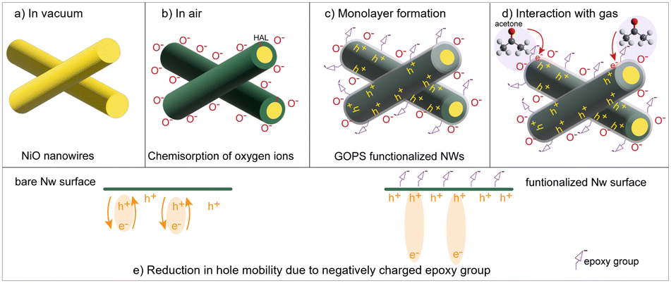 | ||
| Fig. 3 (a) NiO nanowires in a vacuum. (b) Chemisorption of oxygen ions (O−) occurs on the surface of NiO NWs which leads to the formation of a narrow hole accumulation layer (HAL) around the resistive core. (c) monolayer formation on NWs surface that leads to the accumulation of holes near the surface due to the presence of negatively-charged epoxy groups of GOPS. (d) Enhanced interaction with acetone gas that leads to an increase in the electron-hole recombination as compared to bare NiO NWs. (e) reduction in hole mobility occurs after the functionalization with GOPS. | ||
On the other hand, a significant decrease in the baseline conductance of NiO NWs sensor was observed after the surface functionalization with the GOPS monolayer. This can be explain by considering the effect of negatively charged21 epoxy-groups of GOPS monolayer on the surface carrier density of NiO NWs. It was observed that the presence of negatively charged SAM terminal-groups tends to accumulate the holes near the surface of p-type semiconductors (inversely repel electrons).22 In fact, the SAMs approach has widely been used to improve the charge carrier injection at semiconductor/electrode interface of OFET.23–26 Hence, epoxy groups causes the repulsion of electrons away from the NWs surface (inversely, attracts the holes toward the surface (Fig. 3c)). Consequently, the hole density is increased near the surface, i.e., in HAL. However, even though hole accumulation near the surface increases, their mobility within the NWs is decreased. Specifically, holes are electron vacancies that carry a positive electric charge. Indeed, hole mobility that occurs in the material can be seen as a transfer of an electron to this vacant position (hole) due to attractive force between them. This transfer of electrons results in the filling of a vacant position but leaves behind another vacancy from which electrons moved (Fig. 3e (left)). In this way a hole (vacancy) moves from one position to another (opposite to the electron movement), leading to the p-type conductivity in the semiconductor. The presence of negatively charged monolayer (epoxy groups) on NiO NWs surface pushes the electrons further away from the nearby hole, thus increasing their separation (Fig. 3e (right)). Due to this, electrons are subjected to a weaker attractive force toward the holes than in bare NiO NWs, causing a decrement in hole mobility. Hence, the decrease in the conductivity in NiO NWs after GOPS functionalization is attributed to the decrease in hole mobility caused by negatively charged epoxy groups. Similarly, the accumulation of holes and decrease in mobility of pentacene (p-type) based OFET was observed due to the negatively charged amine and fluorinated terminal-groups of SAM.22
On the other hand, an increase in sensor response after functionalization is observed due to the accumulation of more holes near the surface caused by the monolayer. As specified earlier, the negatively charged epoxy groups of GOPS monolayer cause the accumulation of more holes near the surface and withdrawal of electrons. Thus, when GOPS functionalized NWs are exposed to reducing compounds (acetone and ethanol), a higher donation of electrons as compared to bare NWs occurs (Fig. 3d). This enhanced electron donation causes an increase of electron–hole recombination, leading to a higher relative change in conductance i.e., higher response values for functionalized NWs. Similarly, an increase in response of APTMS functionalized ZnO NWs (n-type) toward acetone is observed due to presence of negatively charged (–NH2) groups on the surface that pushes electron away from the surface.19
In conclusion, NiO nanowires were successfully functionalized by GOPS monolayer for low-temperature VOCs sensing. In particular, the functionalized NGP sensors show superior sensing performance toward ethanol and acetone compared to the bare NiO sensor when operated at 200 °C. The major reason behind this improvement was found to be the accumulation of holes near the surface of NWs caused by negatively charged epoxy groups of GOPS. This accumulation consequently makes the NWs surface more favorable for electron acceptance from the reducing gases, hence improving their sensing response. Compared to other reported strategies presented in literature (Table S3, ESI†), the SAM functionalization approach proves to be superior in improving sensing characteristics.
This work was partially funded by NATO Science for Peace and Security Programmer (SPS) under grant G5634 AMOXES – “Advanced Electro-Optical Chemical Sensors”, MIUR “Smart Cities and Communities and social innovation” project titled “SWaRM Net/Smart Water Resource Management Networks, and Regione Lombardia Call Hub Ricerca e Innovazione, within the project “MoSoRe@ Unibs—Infrastrutture e servizi per la Mobilità Sostenibile e Resiliente”.
Conflicts of interest
There are no conflicts to declare.References
- H.-J. Kim and J.-H. Lee, Sens. Actuators, B, 2014, 192, 607–627 CrossRef CAS.
- N. Kaur, M. Singh and E. Comini, Langmuir, 2020, 36, 6326–6344 CrossRef CAS PubMed.
- N. Kaur, E. Comini, D. Zappa, N. Poli and G. Sberveglieri, Nanotechnology, 2016, 27, 205701 CrossRef CAS PubMed.
- S. Park, H. Kheel, G.-J. Sun, S. K. Hyun, S. E. Park and C. Lee, Bull. Korean Chem. Soc., 2016, 37, 713–719 CrossRef CAS.
- M. Govindhan, B. Sidhureddy and A. Chen, ACS Appl. Nano Mater., 2018, 1, 6005–6014 CrossRef CAS.
- F. Meng, T. Qi, J. Zhang, H. Zhu, Z. Yuan, C. Liu, W. Qin and M. Ding, IEEE Trans. Ind. Electron., 2022, 69, 960–970 Search PubMed.
- N. Kaur, D. Zappa, M. Ferroni, N. Poli, M. Campanini, R. Negrea and E. Comini, Sens. Actuators, B, 2018, 262, 477–485 CrossRef CAS.
- N. Kaur, D. Zappa, V.-A. Maraloiu and E. Comini, Adv. Funct. Mater., 2021, 2104416 CrossRef CAS.
- C. Wang, X. Cui, J. Liu, X. Zhou, X. Cheng, P. Sun, X. Hu, X. Li, J. Zheng and G. Lu, ACS Sens., 2016, 1, 131–136 CrossRef CAS.
- C. Li, P. G. Choi, K. Kim and Y. Masuda, Sens. Actuators, B, 2022, 367, 132143 CrossRef CAS.
- R. Miao and W. Zeng, Mater. Lett., 2016, 171, 200–203 CrossRef CAS.
- A. Ulman, Chem. Rev., 1996, 96, 1533–1554 CrossRef CAS PubMed.
- E. Macchia, K. Manoli, B. Holzer, C. Di Franco, R. A. Picca, N. Cioffi, G. Scamarcio, G. Palazzo and L. Torsi, Anal. Bioanal. Chem., 2019, 411, 4899–4908 CrossRef CAS PubMed.
- M. Singh, N. Kaur, A. Casotto, L. Sangaletti, N. Poli and E. Comini, J. Mater. Chem. A, 2022, 10, 3178–3189 RSC.
- E. Orgiu, N. Crivillers, J. Rotzler, M. Mayor and P. Samorì, J. Mater. Chem., 2010, 20, 10798 RSC.
- S. Krämer, R. R. Fuierer and C. B. Gorman, Chem. Rev., 2003, 103, 4367–4418 CrossRef PubMed.
- F. Parmigiani and L. Sangaletti, J. Electron Spectrosc. Relat. Phenom., 1999, 98–99, 287–302 CrossRef CAS.
- N. Pauly, F. Yubero, F. J. García-García and S. Tougaard, Surf. Sci., 2016, 644, 46–52 CrossRef CAS.
- M. Singh, N. Kaur, G. Drera, A. Casotto, L. S. Ermenegildo and E. Comini, Adv. Funct. Mater., 2020, 30, 2003217 CrossRef CAS.
- A. K. Y. Wong and U. J. Krull, Anal. Bioanal. Chem., 2005, 383, 187–200 CrossRef CAS PubMed.
- G. Tan, K. Ouyang, H. Wang, L. Zhou, X. Wang, Y. Liu, L. Zhang and C. Ning, J. Mater. Sci. Technol., 2016, 32, 965 Search PubMed.
- S. Kobayashi, T. Nishikawa, T. Takenobu, S. Mori, T. Shimoda, T. Mitani, H. Shimotani, N. Yoshimoto, S. Ogawa and Y. Iwasa, Nat. Mater., 2004, 3, 317–322 CrossRef CAS PubMed.
- X. Cheng, Y.-Y. Noh, J. Wang, M. Tello, J. Frisch, R.-P. Blum, A. Vollmer, J. P. Rabe, N. Koch and H. Sirringhaus, Adv. Funct. Mater., 2009, 19, 2407–2415 CrossRef CAS.
- I. Bâldea, Faraday Discuss., 2017, 204, 35–52 RSC.
- M. Singh, N. Kaur and E. Comini, J. Mater. Chem. C, 2020, 8, 3938–3955 RSC.
- I. Campbell, S. Rubin, T. Zawodzinski, J. Kress, R. Martin, D. Smith, N. Barashkov and J. Ferraris, Phys. Rev. B: Condens. Matter Mater. Phys., 1996, 54, R14321–R14324 CrossRef CAS PubMed.
Footnote |
| † Electronic supplementary information (ESI) available. See DOI: https://doi.org/10.1039/d2cc06530d |
| This journal is © The Royal Society of Chemistry 2023 |