
 Open Access Article
 This Open Access Article is licensed under a
 Creative Commons Attribution 3.0 Unported Licence
Multifunctional flexible ferroelectric thick-film structures with energy storage, piezoelectric and electrocaloric performance†
Matej
Sadl
 ab,
Uros
Prah
c,
Veronika
Kovacova
c,
Emmanuel
Defay
c,
Tadej
Rojac
ab,
Andrej
Lebar
de,
Joško
Valentinčič
d and
Hana
Ursic
*ab
ab,
Uros
Prah
c,
Veronika
Kovacova
c,
Emmanuel
Defay
c,
Tadej
Rojac
ab,
Andrej
Lebar
de,
Joško
Valentinčič
d and
Hana
Ursic
*ab
aElectronic Ceramics Department, Jožef Stefan Institute, Jamova cesta 39, 1000 Ljubljana, Slovenia. E-mail: hana.ursic@ijs.si
bJožef Stefan International Postgraduate School, Jamova cesta 39, 1000 Ljubljana, Slovenia
cMaterials Research and Technology Department, Luxembourg Institute of Science and Technology, Belvaux, Luxembourg
dFaculty of Mechanical Engineering, University of Ljubljana, Aškerčeva cesta 6, 1000 Ljubljana, Slovenia
eFaculty of Health Sciences, University of Ljubljana, Zdravstvena pot 5, 1000 Ljubljana, Slovenia
First published on 10th July 2023
Abstract
As a major challenge, sustainable energy management and energy self-sufficiency require microsystems that manage multiple energy operations in a single device. In this work, flexible thick-film structures with promising energy storage and electrocaloric cooling capabilities as well as piezoelectric properties are developed. The functional thick-film layer is based on relaxor-ferroelectric 0.65Pb(Mg1/3Nb2/3)O3–0.35PbTiO3 (PMN–35PT) directly deposited on a flexible polyimide substrate by an aerosol deposition method. The thick-film structures exhibit a promising recoverable energy-storage density of 10.3 J cm−3. After extensive bending tests, the structures showed no signs of degradation. The high bendability and durability are confirmed by stable energy storage properties after bending up to a radius of 1.5 mm (2.4% bending strain) and 105 repeated bending cycles. The developed thick-film structures also exhibit a piezoelectric coefficient d33 of ∼80 pm V−1. Using two direct electrocaloric measurement methods, we demonstrated that the electrocaloric temperature change in the prepared PMN–35PT thick-film structures reaches a maximum of 0.87 K at 63.5 °C and 300 kV cm−1, which exceeds the value of 0.72 K at ∼65 °C and 60 kV cm−1 reported for bulk ceramics of the same composition. The PMN–35PT thick films prepared here are thick-film structures with excellent flexibility, promising for future multifunctional microsystems that manage multiple energy operations, enabling comprehensive energy harvesting, storage and conversion to thermal energy.
Introduction
In our increasingly interconnected world, new trends for sustainable energy management, including energy harvesting, storage and conversion, in miniature devices have emerged.1–4 Ferroelectric ceramics are thus becoming increasingly important and their miniaturization is turning out to be critical.3,5 There is a need for microsystems that manage multiple energy operations in a single device, thus offering all-in-one energy harvesting, storage and conversion.1–4,6Piezoelectric energy harvesting is one of the most interesting energy harvesting principles in the microscale because it offers great potential for harvesting kinetic energy, e.g., from mechanical motions, flow and vibrations, which are available in many fields such as transportation, household, in-water applications, microfluidics, body motion and in vivo energy for biomedical applications.7,8 Piezoelectric energy harvesting is usually realized using ferroelectric materials as they have an outstanding electro-mechanical coupling factor and piezoelectric coefficient.9
Dielectric capacitors are used for the capacitive energy storage in pulsed power and power-conditioning electronic applications.10 Since their non-linear polarization-electric field hysteresis can be easily modified, ferroelectric materials can achieve high energy-storage density and efficiency, which makes them promising for energy-storage.
The conversion of electrical energy to thermal energy is currently dominated by a well-established vapor-compression cooling technology, which is environmentally problematic and poorly energy efficient. Significant improvements in energy efficiency and environmental safety can be achieved by alternative solid-state cooling through the electrocaloric (EC) effect, which also allows miniaturization of cooling devices.11–15 Despite the possibility of miniaturization of EC cooling technology, there is a lack of reports addressing the EC effect using direct measurement methods in ceramic thin (below 1 µm) and thick films (up to 100 µm).16–18 EC materials in form of bulk ceramics show promising and well-characterized EC cooling performance. However, despite the miniaturization concept, it is not possible to scale down bulk ceramics to the micrometer level for cooling flexible and portable electronics, so thick film technology must be used for this purpose.19,20 A spray-coating method for depositing of a few micrometer thick ceramic films at room temperature, known as the aerosol deposition (AD) method, is attracting increasing attention.21–26 Recently, it has been shown that nano-grained micrometer-thick films can be deposited on low-melting point substrates such as polymers.27–30 Such ceramic-polymer structures allow not only great flexibility but also reliable determination of the EC effect using direct EC measurement methods.17
Numerous studies have presented self-charging power systems with combined energy harvesting and storage. For example, mechanical energy is harvested and stored in capacitive, electrochemical or battery storage devices that can power, for example, medical health monitoring and wearable smart electronics.4,31–36 However, there are no reports of elements with combined energy harvesting, storage and EC cooling capabilities determined by direct measurement methods, especially in the form of thin or thick films that can also be implemented in flexible applications.
Relaxor-ferroelectrics (1–x)Pb(Mg1/3Nb2/3)O3–xPbTiO3 (PMN–100xPT) exhibit good piezoelectric, energy storage and electrocaloric properties. For example, PMN–35PT bulk ceramics show high piezoelectric coefficients (d33 up to 700 pC N−1)37–39 and high energy storage potential due to low dielectric losses (i.e., 0.04 at 1 kHz).39,40 In addition, PMN–35PT bulk ceramics also exhibit electrocaloric properties, namely 0.9 K at 60 kV cm−1 and 107 °C.41,42 However, for miniaturization, electronic ceramic components must be fabricated in the form of thin or thick films.
In this work, we prepared several micrometer thick PMN–35PT films on flexible polyimide (PI) substrates. We used the AD method, which allows the deposition of fully dense ceramic thick films with exceptional adhesion properties on any substrate materials, including polymers.21,22 The fabricated PMN–35PT thick films are dense and after thermal annealing at moderate temperatures (400 °C) they exhibit promising recoverable energy storage density (Urec = 10.3 J cm−3 at 1000 kV cm−1), piezoelectric coefficient (d33 ∼80 pm V−1) and EC temperature change (ΔTEC = 0.87 K at 63.5 °C), as well as exceptional flexibility (tolerating 2.4% bending strain). Thus, the PMN–35PT thick films prepared here are flexible thick film structures with multifunctional properties that enable energy harvesting, storage and conversion to thermal energy.
Materials and methods
The 0.65Pb(Mg1/3Nb2/3)O3–0.35PbTiO3 ceramic powder was prepared by mechanochemical-activation-assisted synthesis, followed by furnace annealing in air at 900 °C and final planetary ball milling. A detailed description of the powder processing can be found in ref. 28. Prior to aerosol deposition, the PMN–35PT powder was sieved through an 80 µm sieve and vacuum dried at 100 °C and 10 mbar for 12 h. A commercial polyimide (PI) foil (Kapton® HN, DuPont, DE, USA) with a thickness of 125 µm served as substrate. The bottom Cr/Au electrode was deposited on the substrate (first 30 nm Cr, then ∼1 µm Au) using a RF-magnetron sputtering system (5 Pascal, Italy). The AD equipment was provided by InVerTec, Germany and the schematic of the setup is shown elsewhere.43 The process parameters of AD are listed in (ESI† S1). After AD, the samples were cleaned with ethanol and some of them also thermally annealed at 400 °C for 1 h with heating and cooling rates of 2 K min−1. Further on, non-annealed and annealed samples will be referred to as “as-deposited” and “annealed”.X-ray diffraction (XRD) analysis was performed under the same conditions as in ref. 28. A high-resolution diffractometer (X’Pert PRO, PANalytical, The Netherlands) was used to record diffraction patterns using Cu–Kα1 radiation in the Bragg–Brentano geometry and in a 2θ range of 10°–120°. The Topas R package (version 2.1, Bruker AXS GmbH, Germany) was used for Rietveld refinement and the line-profile of the samples was fitted using the Fundamental Parameters Approach (FPA).44 The FPA uses the geometrical properties of the diffraction experiment to build up the instrumental line width from first principles. It thus allows an explicit determination of the sample-dependent line-broadening contributions to the peak profile, which are dominated by the microstrain and the broadening of the crystallite size.45 A tetragonal P4mm structure was used to calculate the crystallite size and microstrain of the PMN–35PT solid solution in powders and films. A cubic (Fm![[3 with combining macron]](https://www.rsc.org/images/entities/char_0033_0304.gif) m) crystal structure was used to fit the Au reflections originating from the bottom electrode. The agreement factors of the Rietveld refinement are listed in ESI† S2.
m) crystal structure was used to fit the Au reflections originating from the bottom electrode. The agreement factors of the Rietveld refinement are listed in ESI† S2.
Scanning electron microscopy (SEM) and piezo-response force microscopy (PFM) analyses of the surfaces and cross-sections of polished thick films were performed using a field-emission scanning electron microscope (FE-SEM, JSM-7600F, JEOL, Japan) and an atomic force microscope (AFM; MFP-3D, Asylum Research, CA, USA). Details of sample preparation and SEM and PFM analyses are in ref. 28 and 46. The images were scanned in dual AC resonance-tracking (DART) mode. For PFM imaging, an electrical voltage of 15–25 V and a frequency of ∼350 kHz were used. The thickness and porosity of the thick films were evaluated from SEM cross-sectional images. For the estimation of porosity, the Image Tool software (UTHSCSA Image Tool Version 3.00. 2002,47) was used. The local PFM amplitude and phase hysteresis loops were measured in DART switching spectroscopy mode (DART-SS). The measurements were performed on the polished surface samples in switching spectroscopy off-electric-field mode using the pulsed DC step signal and the superimposed AC drive signal, as described in.48 The sequence of increasing electric field steps was used with 20 Hz and a maximum amplitude of 100 and 70 V for the as-deposited and annealed samples, respectively. Three cycles were measured with the triangular envelope frequency of 0.2 Hz. A superimposed sinusoidal AC signal with an amplitude of 20 V and a frequency of ∼350 kHz was applied.
For the electrical measurements, top Au electrodes with diameters of 1.5 and 3.0 mm were deposited by a RF-magnetron sputtering. The aixACCT TF analyzer 2000 (aixACCT Systems GmbH, Germany) was used to measure the polarization–electric field (P–E) hysteresis loops of the films. The waveform of the applied electric field was unipolar and sinusoidal at 100 Hz. For the energy storage calculations, the second P–E loop measured in sequence was used rather than the first. The P–E loops measured before and after bending tests were performed with an electric field of 500 kV cm−1.
Static tensile bending tests of thick film samples were performed by conforming the thick film samples to steel cylinders with specified radii between 12 and 1.5 mm. The bending strain was calculated from the bending curvature using the multilayer model, which is described in ESI† S3. Fatigue tensile bending tests were performed on a linear sliding moving stage. The custom-build sample holder allowed bending of free-standing samples (ESI† video). The minimum bending radius and bending frequency were kept constant at 3 mm and 1 Hz, respectively. The minimum bending radius was set using a 2D laser displacement sensor (sensor head LJ-G080, controller LJ-G5001, Keyence, Japan). The maximum number of bending cycles was 105.
Converse piezoelectric coefficient (d33) measurements of thick film samples glued on a rigid substrate were performed with a home-made setup based on an optical-fiber sensor (MTI 2100 Fotonic Sensor; MTI Instruments Inc., NY, USA) equipped with a SRS DS360 voltage generator (Stanford Research Systems Inc., CA, USA), Trek 609E-6 high-voltage amplifier (Trek Inc., NY, USA), DSOX1204A oscilloscope (Keysight Technologies, CA, USA), SR 560 low-noise pre-amplifier (Stanford Research Systems Inc., CA, USA) and SRS 830 DSP lock-in amplifier (Stanford Research Systems Inc., CA, USA). Due to the low displacement signals (on the nm level) a lock-in technique was used and the d33 was determined from the first-order harmonic strain response. A subcoercive electric field (up to 80 kV cm−1) was applied in a bipolar and sinusoidal waveform at 10 Hz. Prior to the measurements, the samples were poled by applying a DC electric field of 500 kV cm−1 at room temperature for 15 min.
Direct EC measurements were performed using two different thermometric methods. One is high-resolution calorimetry based on temperature measurements with a small thermistor attached to the sample and the other is based on temperature measurements with a non-contact infrared (IR) camera, referred to here as the IR camera method. For both measurement methods, a sample with a diameter of the top Au electrode of 3.0 mm was used.
For the calorimeter method, the sample was prepared by gluing Cu wires with a diameter of 80 µm to the top and bottom electrodes with an Ag-filled epoxy adhesive (EPO-TEK® EE129-4, Epoxy Technology, MA, USA). A miniature radial glass bead thermistor (GR500KM4261J15, Measurement Specialties, VA, USA) was bonded to the top electrode with a general-purpose adhesive. During measurements, the temperature was stabilized with an accuracy of ±1 mK using a modified differential scanning calorimeter (Netzsch DSC 204 F1, Germany). In the DSC measurement cell, the sample was kept in air by suspending it from the sample holder with Cu wires. A Pt1000 temperature probe was used to control the ambient temperature. The EC induced temperature change of the sample was measured with the thermistor whose resistance was monitored with a Keithley 2100 digital multimeter (Keithley Instruments, OH, USA). To trigger the EC effect, the DC electric field was applied to the sample with a step-like waveform and a period of 200 s (i.e., 100 s on-field and 100 s off-field) using a Keithley High Voltage Source-Measure Unit 237 (Keithley Instruments, OH, USA). Measurements were performed in a temperature range of 31–82 °C. After stabilization at a certain temperature, the electric field was applied with progressively increasing amplitude from 100 to 250 kV cm−1 with a step of 50 kV cm−1. A heat capacity analysis was performed to determine the correction factor (k), i.e., the ratio between the intrinsic EC temperature change (ΔTEC) of the PMN–35PT film and the ΔT measured with calorimetry (ESI† S4). Further details about the method can also be found in ref. 17.
For the IR camera measurements, a ∼3.5 µm thick black ink layer was printed on the top Au electrode to increase the emissivity of the sample surface and to allow accurate monitoring of its temperature. In addition, no further sample preparation steps were required for these measurements. Measurements were performed using an IR camera (FLIR X6580sc, OR, USA) with a forced-cooling quantum InSb detector. The DC electric field, i.e., a step-like waveform with a period of 1 s (i.e., 0.5 s on-field and 0.5 s off-field), was generated with a Keithley 3390 arbitrary waveform generator (Keithley Instruments, OH, USA) and a Trek 2220 high-voltage amplifier (Trek Inc., NY, USA) and monitored with a DSO5014A oscilloscope (Agilent Technologies, CA, USA). Ambient temperature was controlled using a THM S600 temperature stage (Linkam Scientific Instruments, UK) with active cooling by liquid N2 (LNP95). Measurements were performed in a temperature range of 11–72 °C. After stabilization at a given temperature, three cycles of each electric field amplitude (i.e., 200, 250 and 300 kV cm−1) were applied. Numerical modelling of heat dissipation was performed to evaluate the ratio between the adiabatic ΔTEC of the PMN–35PT film and the ΔT measured at the top of the black ink layer. A finite element method was introduced using the heat transfer module of COMSOL Multiphysics software (version 5.6) and a 2D model was created assuming the dimensions of the real sample. More information about the complete EC measurement procedure using the IR camera (black ink emissivity calculations, IR camera acquisition, details of the numerical model and its refinement with the experimental data) can be found in ref. 17.
Results and discussion
Structural and microstructural analysis of PMN–35PT thick films
To confirm a successful aerosol deposition of PMN–35PT thick films on golden polyimide (Au/PI) substrates, the crystal structure and microstructure of as-deposited and thermally annealed samples were analysed by XRD and SEM, respectively. The XRD patterns of the PMN–35PT powder and the corresponding as-deposited and annealed films are shown in Fig. 1(a) and (b). No secondary phases were detected; all reflections correspond to the perovskite phase except for two Au reflections corresponding to the bottom electrode. The thick films show a remarkable peak broadening due to a decrease in crystallite size and/or an increase in microstrain. | ||
| Fig. 1 (a) XRD patterns in the 2θ range of 20–60° for PMN–35PT powder, as-deposited and annealed thick films; (b) magnified view of (110) reflection. The diffraction peaks corresponding to the gold and perovskite phases are indexed according to the cubic notation (JCPDS 04-0784 and 81-0861, respectively). The corresponding (c) crystallite size and (d) microstrain were determined using Rietveld refinement. SEM micrographs of as-deposited (e and g) and annealed (f and h) films in cross-section (e and f) and surface (g and h) views. The PI substrate is not visible in panels (e) and (f). | ||
Quantitative Rietveld refinement analysis was performed to calculate crystallite size and microstrain (Fig. 1(c) and (d)). The PMN–35PT powder contains large crystallites (146 nm ± 3 nm) and a relatively low microstrain (8.4 × 10⁻⁴ ± 0.3 × 10⁻⁴). After the AD process, the formed thick films exhibit a significantly smaller crystallite size (15.4 nm ± 0.3 nm) compared to the powder (10-fold reduction after AD) and a significant increase in microstrain (20.9 × 10⁻⁴ ± 2.6 × 10⁻⁴). The decrease in crystallite size and the increase in microstrain are due to the high-energy particle collisions during AD. It has been shown that only a sufficient decrease in crystallite size and increase in microstrain can lead to successful deposition that forms consolidated thick films.24 Additional annealing of the films has a rather small effect on the crystallite size (17.5 nm ± 0.3 nm) and a moderate effect on the microstrain (17.9 × 10⁻⁴ ± 2.3 × 10⁻⁴), both shown in (Fig. 1(c) and (d)).
The SEM analysis of the as-deposited and annealed PMN–35PT thick films shows no significant difference in microstructure (Fig. 1(e)–(h)). Micrographs of cross-sections show films with a thickness of 2.5 µm and Au bottom electrodes (Fig. 1(e) and (f)). Both as-deposited and annealed PMN–35PT thick films exhibit high density (estimated porosity as low as 1%) and good adhesion to Au/PI substrates. On the cross-sectional micrographs nm-sized pores can be seen, while the surface micrographs show a typical surface morphology (Fig. 1(g) and (h)).
Energy-storage properties and flexibility of PMN–35PT thick films
The unipolar P–E hysteresis loops were measured on as-deposited and thermally annealed PMN–35PT thick films (Fig. 2(a)). The as-deposited films show a linear behaviour at a low electric field (200 kV cm−1) and a more lossy dielectric behaviour with increasing electric field (up to 1000 kV cm−1). Annealing of the films leads to relaxor-ferroelectric P–E behaviour with a slimmer hysteresis. Such improvement of P–E behaviour is a consequence of thermally activated stress relaxation and recombination of charged defects.26,49,50 The shape of the P–E loops is maintained even at lower driving frequencies (ESI† S5). The maximum polarization reaches 42 µC cm−2 at 1000 kV cm−1. The films can withstand very high electric fields, which makes them promising for capacitive energy-storage applications, especially when high electric fields are required. Weibull analysis was performed to evaluate the dielectric breakdown strength, which reaches 1033 and 968 kV cm−1 for the as-deposited and annealed thick films, respectively (ESI† S6).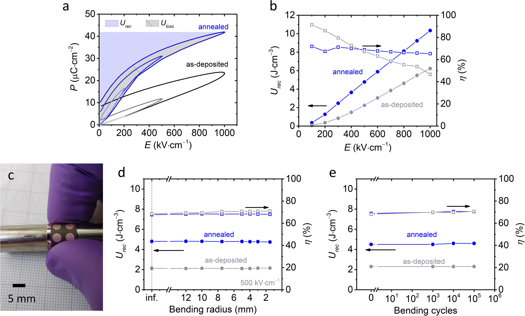 | ||
| Fig. 2 (a) Unipolar P–E hysteresis loops of as-deposited (grey) and annealed (blue) PMN–35PT thick films measured up to 200 kV cm−1, 500 kV cm−1 and 1000 kV cm−1. Urec and Uloss of the annealed layer are shown by the blue and grey patterned areas, respectively. (b) The electric field dependence of Urec and η for the deposited and annealed thick films. (c) Photograph of the sample under tensile bending test. (d) Urec and η values (at 500 kV cm−1) at different bending radii. (e) Urec and η values at 500 kV cm−1 as a function of bending cycles measured after the fatigue test (repetitive bending down to a radius of 3 mm). The lines between the data points are only a guide for the eye. | ||
The most important energy-storage properties are recoverable energy-storage density (Urec) and energy-storage efficiency (η). Urec is the energy recovered during discharge and is obtained by integrating the area between the discharge curve and the ordinate (blue patterned area in Fig. 2(a)). The η is the ratio between the recovered and stored energy (η = Urec/(Urec + Uloss)), where Uloss represents the hysteresis losses, the area between the charge and discharge curves (grey patterned area in Fig. 2(a)).
Fig. 2(b) shows Urec and η of as-deposited (grey) and annealed (blue) thick films. The Urec value increases almost linearly with electric field, but the increase is much higher for annealed thick films. At 1000 kV cm−1, the Urec value reaches 6.2 and 10.3 J cm−3 for as-deposited and annealed films, respectively. On the other hand, the η-value decreases with increasing electric field. In as-deposited films, η decreases from 91% at 100 kV cm−1 to 47% at 1000 kV cm−1 (Δη = 44%). In annealed thick films, the decrease in η is much smaller (Δη = 7%). η decreases from 72% at 100 kV cm−1 to 65% at 1000 kV cm−1. At 1000 kV cm−1 the energy storage properties of the annealed PMN–35PT films on the PI substrates are comparable to other AD thick films on conventional, more expensive Pt/Ti/SiO2/Si substrates. The reported Urec and η values (at 1000 kV cm−1) of AD thick films on Pt/Ti/SiO2/Si substrates range from 9.7 to 15.1 J cm−3 and from 70% to 84%, respectively.51–55 However, further improvement of the Urec is possible by increasing the dielectric breakdown strength, e.g., PMN–35PT films reported by Park et al. reach 2000 kV cm−1, leading to a Urec of 35 J cm−3.53
To evaluate the flexibility of the PMN–35PT films on PI substrate, the energy-storage properties were measured after tensile bending (Fig. 2(c)). Urec and η measured at 500 kV cm−1 are shown in Fig. 2(d) after reaching different bending radii. Both the deposited and annealed thick films exhibit excellent flexibility, as the energy storage properties did not deteriorate after bending down to a radius of 1.5 mm, i.e., a bending strain of 2.4%. In addition, visual inspection of the films after bending did not reveal any damage on the thick film surfaces.
In the next experiment, the flexural fatigue tolerance of the films was evaluated by repeated tensile bending down to a radius of 3 mm (1.2% bending strain). Fig. 2(e) shows the energy storage properties of the deposited and annealed films measured at 500 kV cm−1 after 103, 104 and 105 repetitions. Urec and η remain stable and do not show significant variations even after 105 bending cycles. Since the PMN–35PT films on the PI substrate showed no degradation in energy-storage performance after extensive bending tests applying substantially high bending strain, they have the potential to be integrated into various flexible electronic systems.
Electromechanical properties of PMN–35PT thick films at the micro and macro scale
PFM was performed to study the local piezoelectric response and to image the ferroelectric domain structure. A schematic representation of a PFM experiment of the samples in cross-section is shown in Fig. 3(a) and the PFM out-of-plane amplitude images of polished sample surfaces and cross-sections are shown in Fig. 3(b)–(d), (g) and (h). The images confirm piezoelectrically active grains with size in the order of 100 nm. From the out-of-plane PFM amplitude images of the samples in cross-section, it is evident that both films are piezoelectrically active throughout the film thickness. All other components of the investigated sample, i.e., the bottom Au electrode, the PI substrate and the encapsulating epoxy resin above the film, showed no piezoelectric response (dark areas in Fig. 3(b)). Switching spectroscopy was performed on thick film surfaces and shows a local hysteresis loop of the PFM phase (Fig. 3(e) and (i)) and PFM amplitude (Fig. 3(f) and (j)). The PFM phase response shows clear piezoelectric switching behaviour in both films (Fig. 3(e) and (i)). However, in the annealed films, the PFM switching is more distinguished and the local hysteresis loops are therefore more saturated (Fig. 3(i)).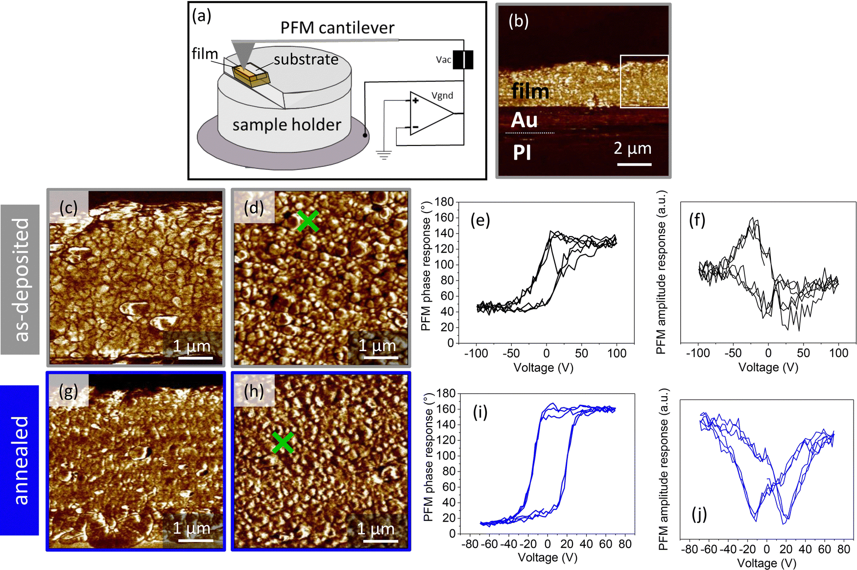 | ||
| Fig. 3 (a) Experimental setup for PFM measurements on samples in cross-section. For more information, see ref. 46. (b) PFM out-of-plane amplitude image of as-deposited PMN–35PT thick film/Au electrode/PI substrate in cross-section view. (c) Higher magnification of PFM out-of-plane amplitude image of the as-deposited film marked by the white square on panel (b). (d) PFM out-of-plane amplitude image from the surface of as-deposited film. Please note that piezoelectric performance cannot be quantitatively evaluated because the images were scanned in DART mode to improve the signal-to-noise ratio. The local (e) PFM phase and (f) PFM amplitude hysteresis loops measured at the location marked by the green cross in panel (d). PFM out-of-plane amplitude image of the annealed film in (g) cross-section and (h) surface views. The local (i) PFM phase and (j) PFM amplitude hysteresis loops measured at the location marked by the green cross in panel (h). | ||
The macroscopic electromechanical properties of the PMN–35PT thick films were evaluated by measuring converse d33 and tangent of piezoelectric phase angle (tan![[thin space (1/6-em)]](https://www.rsc.org/images/entities/char_2009.gif) δp), as shown in Fig. 4. The d33 reaches 14 pm V−1 for as-deposited films and 75–82 pm V−1 for annealed films, depending on the amplitude of applied electric field. A five times higher d33 value for thick films after annealing indicates that stress relaxation has an effect on the piezoelectric response. In addition, the annealed films also show an increase in d33 with electric field amplitude coupled to an increase of tan
δp), as shown in Fig. 4. The d33 reaches 14 pm V−1 for as-deposited films and 75–82 pm V−1 for annealed films, depending on the amplitude of applied electric field. A five times higher d33 value for thick films after annealing indicates that stress relaxation has an effect on the piezoelectric response. In addition, the annealed films also show an increase in d33 with electric field amplitude coupled to an increase of tan![[thin space (1/6-em)]](https://www.rsc.org/images/entities/i_char_2009.gif) δp with field. Although weak (relative increase of d33 with field of 8%), this nonlinearity and nonlinear hysteresis are attributed to extrinsic piezoelectric contributions related to irreversible interface dynamics.56–59 A similar increase in the irreversible contribution to the dielectric permittivity was previously demonstrated in PMN–35PT thick films after thermal annealing.30 The as-deposited and annealed films exhibit reasonable tanδp values, i.e., 0.01–0.02 and 0.03–0.04, respectively. The overall electromechanical properties of annealed PMN–35PT thick films are promising for future flexible piezoelectric energy harvesting devices. However, the d33 in aerosol-deposited thick films is limited due to the film-substrate clamping effect60,61 and small grain size.38 For example, screen-printed PMN–35PT thick films on platinized Al2O3 substrates that were annealed at 950 °C exhibit higher d33 (typically between 130 and 170 pC N−1) due to the large grain size.60,62,63 In another study, Han et al. demonstrated the effect of substrate clamping on piezoelectric properties of AD thick films.64 By increasing the film thickness from 1 µm to 55 µm in annealed (700 °C) Pb(Zr0.52Ti0.48)O3 thick films on Si substrates, the effective piezoelectric coefficient d33 increases from 75 pm V−1 to 210 pm V−1,64 indicating on weakening of the clamping effect.
δp with field. Although weak (relative increase of d33 with field of 8%), this nonlinearity and nonlinear hysteresis are attributed to extrinsic piezoelectric contributions related to irreversible interface dynamics.56–59 A similar increase in the irreversible contribution to the dielectric permittivity was previously demonstrated in PMN–35PT thick films after thermal annealing.30 The as-deposited and annealed films exhibit reasonable tanδp values, i.e., 0.01–0.02 and 0.03–0.04, respectively. The overall electromechanical properties of annealed PMN–35PT thick films are promising for future flexible piezoelectric energy harvesting devices. However, the d33 in aerosol-deposited thick films is limited due to the film-substrate clamping effect60,61 and small grain size.38 For example, screen-printed PMN–35PT thick films on platinized Al2O3 substrates that were annealed at 950 °C exhibit higher d33 (typically between 130 and 170 pC N−1) due to the large grain size.60,62,63 In another study, Han et al. demonstrated the effect of substrate clamping on piezoelectric properties of AD thick films.64 By increasing the film thickness from 1 µm to 55 µm in annealed (700 °C) Pb(Zr0.52Ti0.48)O3 thick films on Si substrates, the effective piezoelectric coefficient d33 increases from 75 pm V−1 to 210 pm V−1,64 indicating on weakening of the clamping effect.
 | ||
| Fig. 4 Converse piezoelectric coefficient (d33, left axis) and tangent of piezoelectric phase angle (tanδp, right axis) as a function of electric field amplitude of as-deposited (black) and annealed (blue) PMN–35PT thick films measured at 10 Hz. The lines between the data points are only a guide for the eye. | ||
Electrocaloric properties of PMN–35PT thick films
The EC effect of the prepared PMN–35PT films was measured directly using two different thermometric methods, referred to here as the high-resolution calorimetry and IR camera method. The first method relies on temperature measurements with a small thermistor attached to the sample, while the other method uses a fast IR camera. The choice of two different EC direct methods not only allowed us to validate the results obtained, but also gave us the opportunity to perform the measurements at different electric fields. In particular, the precise temperature stabilization of the calorimeter method allows the measurement of the EC induced ΔT at lower applied electric fields (100–200 kV cm−1), while the fast temperature measurement of the IR camera and thus the use of a shorter electric field pulse allows the application of larger electric fields (up to 300 kV cm−1) without the risk of dielectric breakdown. The difference in the measurement principle is clearly evident in the typically obtained EC cycles and the time scale of the occurrence of EC heating and cooling peaks, where in the case of the calorimetry the peak of the EC induced ΔT is reached after 0.7 s (Fig. 5(a)), while the IR camera records it in 1.5 ms (Fig. 5(b)).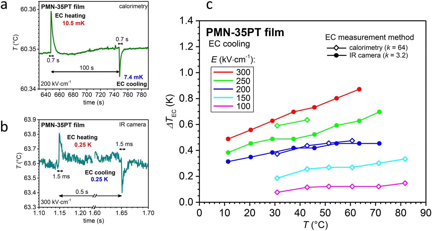 | ||
| Fig. 5 Typical EC cycle obtained by (a) calorimeter method at 60.35 °C and 200 kV cm−1 and (b) IR camera at 63.6 °C and 300 kV cm−1. (c) Temperature- and field-dependent ΔTEC values of the annealed PMN–35PT thick films measured by the calorimeter (open squares) and the IR camera (solid circles) methods. | ||
The EC measurements of the as-deposited PMN–35PT thick films by the calorimeter method showed an excessive Joule heating effect (ESI† S4). The latter, which occurs progressively above 100 kV cm−1, completely overshadowed the EC effect. Therefore, an accurate and systematic analysis of the EC effect could only be performed on thermally annealed samples where the Joule heating was negligible. This is consistent with the P–E measurements (Fig. 2(a)), where the shape of the loops indicates a higher electrical conductivity of the as-deposited samples compared to the annealed samples.
The intrinsic ΔTEC of annealed PMN–35PT thick films obtained by both measurement methods at different temperatures and applied electric fields is shown in Fig. 5(c), where the open squares and solid circles represent the data from the calorimeter and the IR camera method, respectively. The evaluated ΔTEC is composed of two parts, namely the measured ΔT and the correction factor (k), which indicates the ratio between adiabatic ΔTEC and measured ΔT and is applied specifically for each method (see ESI† S4 and ref. 17 for more details). Despite different measurement principles and a difference in the magnitude of the k (i.e., 3.2 for the IR camera compared to 64 for the calorimeter method), the results of the two methods agree quite well, especially at lower electric fields, while the results at higher fields, i.e., 250 kV cm−1, show a slightly larger discrepancy. The main reason for this discrepancy is most likely due to the increased measurement uncertainty that occurs differently for each measurement method. For the calorimeter method, the main contribution to uncertainty results from the determination of the correction factor (i.e., the determination of the heat capacity values of EC active and non-active components), whereas for the IR camera method, the main source of error is related to the larger noise of the temperature measurement (estimated deviation of 30 mK). For the calorimeter method the estimated uncertainty level is 21%, while for the IR camera method the estimated uncertainty levels are ranging from 18% to 29%. Further details can be found in ESI† S4, where different contributions to the overall uncertainty are estimated for the two methods. The ΔTEC shows an increasing trend with increasing temperature over the entire measured temperature range (11–82 °C), which is consistent with the increase in the dielectric permittivity over this temperature range (ESI† S7). When the maximum electric field of 300 kV cm−1 was applied, the intrinsic ΔTEC in the PMN–35PT films reached a value of 0.63 K at 29 °C. The maximum intrinsic ΔTEC of 0.87 K was measured at 63.5 °C (Fig. 5(c)).
The determined maximum ΔTEC value is comparable to the maximum value measured in PMN–35PT bulk ceramic samples, which is reported as 0.9 K at 107 °C and 60 kV cm−141 and 0.55 K at 115 °C and 30 kV cm−1.42 However, when comparing the ΔTEC values of PMN–35PT bulk ceramics and aerosol deposited thick films at similar temperature, i.e. ∼65 °C, the ΔTEC value of thick films exceeds the value reported for bulk ceramics (i.e. 0.72 K at 60 kV cm−1).41 This indicates a great potential of AD thick films for EC cooling applications. In addition, due to the much smaller thickness of the films compared to bulk ceramics, about five times lower voltage is required to apply about five times larger electric field. Also note that the prepared films can withstand high electric fields. This is due to the high dielectric breakdown strength of the aerosol-deposited PMN–35PT thick films associated with a very high density and small grain size, as can be seen from the microstructures shown in Fig. 1(f) and (h). Therefore, the aerosol deposition technique opens a new opportunity in the field of EC applications, which could lead to the fabrication of more efficient EC thick film structures for cooling future flexible electronics. These results could stimulate further research in this field to fabricate EC thick films on polymer substrates using the best EC materials, e.g., lead-based Pb(Sc0.5Ta0.5)O3,65,66 and lead-free BaTiO367 and to investigate the effects of bending on their EC performance.
Conclusions
To provide a concept for multiple energy operations in a single device, we prepared ferroelectric PMN–35PT thick films on flexible structures with energy storage, piezoelectric and EC performance. For the deposition of PMN–35PT thick films on polyimide substrates, the AD method was used because it enables deposition of ceramics on any substrate materials due to its room temperature impact consolidation mechanism. The as-deposited 2.5 µm thick PMN–35PT films on PI substrates were single-phase and exhibited a dense microstructure with porosity of only 1%. After thermal annealing at 400 °C, the microstructure did not change. The crystallite size remained similar as prior annealing (∼18 nm), while the decrease in microstrain after annealing indicates a relaxation of stresses. As a result of the high density, the thick films exhibit high dielectric breakdown strength of ∼1000 kV cm−1.The annealed PMN–35PT thick films exhibit relaxor-ferroelectric character with high electric polarization of 42 µC cm−2 and promising energy storage properties, namely Urec of 10.3 J cm−3 and η of 65% at 1000 kV cm−1. Both the as-deposited and annealed films exhibit high bendability and durability, as confirmed by stable energy storage properties after bending to a radius of 1.5 mm (2.4% bending strain) and repeating 105 bending cycles. A piezoelectrically active, fine-grained microstructure was found in both as-deposited and annealed films by PFM. The annealed films exhibit a piezoelectric coefficient d33 of ∼80 pm V−1, which was determined by macroscopic displacement measurements in sub-coercive regime.
Moreover, this work is one of not so many reports to show reliable direct EC measurements on ceramic thick films.16,17 The annealed PMN–35PT thick films were measured by two methods: high-resolution calorimetry and IR camera. The measured intrinsic ΔTEC of both methods are in reasonable agreement, which reinforces the reliability of the measurement results. The ΔTEC in the annealed PMN–35PT films reached a maximum of 0.87 K at 63.5 °C and 300 kV cm−1, which is higher than the previously reported ΔTEC for PMN–35PT bulk ceramics (i.e. 0.72 K at ∼65 °C and 60 kV cm−141). This is due to the high dielectric breakdown strength of the aerosol-deposited PMN–35PT thick films, which is associated with a very high density and a small sub-micrometre grain size. Therefore, aerosol deposition technology opens up new opportunities in EC applications that could lead to the fabrication of EC thick-film structures for cooling future electronics.
In conclusion, the PMN–35PT thick films prepared here are multifunctional thick-film structures with flexibility, electrocaloric cooling and energy storage capability, and piezoelectric performance. Further development of such structures could open up new applications for various energy operations and enable comprehensive energy harvesting, storage and conversion to thermal energy.
Conflicts of interest
The authors declare that they have no known competing financial interests or personal relationships that could have appeared to influence the work reported in this paper.Acknowledgements
M. S., T. R., A. L., J. V. and H. U. acknowledge the Slovenian Research Agency (research project J2-3058 and N2-0212, research core funding P2-0105 and P2-0248) and JSI Director's fund 2017-ULTRACOOL. They thank A. Iacomini for discussions and J. Cilenšek, N. Suban and M. Karypidou for help in the laboratory. U. P., V. K. and E. D. acknowledge the Fonds National de la Recherche (FNR) of Luxembourg for support of this work under the BRIDGES2020/MS/15410586/CALPOL/Defay project.References
- J. H. Lee, J. Kim, T. Y. Kim, M. S. Al Hossain, S. W. Kim and J. H. Kim, All-in-one energy harvesting and storage devices, J. Mater. Chem. A, 2016, 4(21), 7983–7999 RSC.
- Y. Zhong, X. Xia, W. Mai, J. Tu and H. J. Fan, Integration of Energy Harvesting and Electrochemical Storage Devices, Adv. Mater. Technol., 2017, 2(12), 1–14 Search PubMed.
- X. Wei, N. Domingo, Y. Sun, N. Balke, R. E. Dunin-Borkowski and J. Mayer, Progress on Emerging Ferroelectric Materials for Energy Harvesting, Storage and Conversion, Adv. Energy Mater., 2022, 12(24), 2201199 CrossRef CAS.
- X. Pu, W. Hu and Z. L. Wang, Toward Wearable Self-Charging Power Systems: The Integration of Energy-Harvesting and Storage Devices, Small, 2018, 14(1), 1702817 CrossRef PubMed.
- H. Huang and J. F. Scott, Ferroelectric Materials for Energy Applications, John Wiley & Sons, 2018 Search PubMed.
- S. Pan, J. Ren, X. Fang and H. Peng, Integration: An Effective Strategy to Develop Multifunctional Energy Storage Devices, Adv. Energy Mater., 2016, 6(4), 1–19 Search PubMed.
- B. Maamer, A. Boughamoura, A. M. R. Fath El-Bab, L. A. Francis and F. Tounsi, A review on design improvements and techniques for mechanical energy harvesting using piezoelectric and electromagnetic schemes, Energy Convers. Manage., 2019, 199, 111973 CrossRef.
- D. Steingart, Power Sources for Wireless Sensor Networks, in Energy Harvesting Technologies, ed. S. Priya and D. J. Inman, Springer US, Boston, MA, 2009, pp. 267–286 Search PubMed.
- N. Sezer and M. Koç, A comprehensive review on the state-of-the-art of piezoelectric energy harvesting, Nano Energy, 2021, 80, 105567 CrossRef CAS.
- H. Palneedi, M. Peddigari, G. T. Hwang, D. Y. Jeong and J. Ryu, High-Performance Dielectric Ceramic Films for Energy Storage Capacitors: Progress and Outlook, Adv. Funct. Mater., 2018, 28(42), 1–33 CrossRef.
- Z. Kutnjak, B. Rožič and R. Pirc, in Electrocaloric Effect: Theory, Measurements, and Applications, Wiley Encyclopedia of Electrical and Electronics Engineering, John Wiley & Sons, Inc., Hoboken, 2015 Search PubMed.
- E. Defay, S. Crossley, S. Kar-Narayan, X. Moya and N. D. Mathur, The electrocaloric efficiency of ceramic and polymer films, Adv. Mater., 2013, 25(24), 3337–3342 CrossRef CAS PubMed.
- M. Valant, Electrocaloric materials for future solid-state refrigeration technologies, Prog. Mater. Sci., 2012, 57(6), 980–1009 CrossRef CAS.
- A. Torelló, P. Lheritier, T. Usui, Y. Nouchokgwe, M. Gérard, O. Bouton, S. Hirose and E. Defay, Giant temperature span in electrocaloric regenerator, Science, 2020, 370(6512), 125–129 CrossRef PubMed.
- L. Mañosa, A. Planes and M. Acet, Advanced materials for solid-state refrigeration, J. Mater. Chem. A, 2013, 1(16), 4925 RSC.
- Y. Liu, J. F. Scott and B. Dkhil, Direct and indirect measurements on electrocaloric effect: Recent developments and perspectives, Appl. Phys. Rev., 2016, 3(3), 031102 Search PubMed.
- U. Prah, M. Sadl, A. Torello, P. Lheritier, V. Kovacova, H. Ursic and E. Defay, Direct Electrocaloric Characterization of Ceramic Films, Small Methods, 2023, 2300212 CrossRef PubMed.
- X. Moya, E. Stern-Taulats, S. Crossley, D. González-Alonso, S. Kar-Narayan, A. Planes, L. Mañosa and N. D. Mathur, Giant Electrocaloric Strength in Single-Crystal BaTiO3, Adv. Mater., 2013, 25(9), 1360–1365 CrossRef CAS PubMed.
- Y. Meng, Z. Zhang, H. Wu, R. Wu, J. Wu, H. Wang and Q. Pei, A cascade electrocaloric cooling device for large temperature lift, Nat. Energy, 2020, 5(12), 996–1002 CrossRef.
- X. Moya and N. D. Mathur, It's not about the mass, Nat. Energy, 2020, 5(12), 941–942 CrossRef.
- J. Akedo, Room temperature impact consolidation (RTIC) of fine ceramic powder by aerosol deposition method and applications to microdevices, J. Therm. Spray Technol., 2008, 17(2), 181–198 CrossRef CAS.
- D. Hanft, J. Exner, M. Schubert, T. Stöcker, P. Fuierer and R. Moos, An overview of the Aerosol Deposition method: Process fundamentals and new trends in materials applications, J. Ceram. Sci. Technol., 2015, 6(3), 147–181 Search PubMed.
- J. Exner, M. Linz, J. Kita and R. Moos, Making powder aerosol deposition accessible for small amounts: A novel and modular approach to produce dense ceramic films, Int. J. Appl. Ceram. Technol., 2021, 18(6), 2178–2196 CrossRef CAS.
- J. Exner, M. Schubert, D. Hanft, J. Kita and R. Moos, How to treat powders for the room temperature aerosol deposition method to avoid porous, low strength ceramic films, J. Eur. Ceram. Soc., 2019, 39(2–3), 592–600 CrossRef CAS.
- T. Nazarenus, J. Kita, R. Moos and J. Exner, Laser-Annealing of Thermoelectric CuFe0.98Sn0.02O2 Films Produced by Powder Aerosol Deposition Method, Adv. Mater. Interfaces, 2020, 7(22), 1–13 Search PubMed.
- U. Eckstein, J. Exner, A. Bencan Golob, K. Ziberna, G. Drazic, H. Ursic, H. Wittkämper, C. Papp, J. Kita, R. Moos, K. G. Webber and N. H. Khansur, Temperature-dependent dielectric anomalies in powder aerosol deposited ferroelectric ceramic films, J. Mater., 2022, 8(6), 1239–1250 Search PubMed.
- M. Sadl, O. Condurache, A. Bencan, M. Dragomir, U. Prah, B. Malic, M. Deluca, U. Eckstein, D. Hausmann, N. H. Khansur, K. G. Webber and H. Ursic, Energy-storage-efficient 0.9Pb(Mg1/3Nb2/3)O3–0.1PbTiO3 thick films integrated directly onto stainless steel, Acta Mater., 2021, 221, 117403 CrossRef CAS.
- M. Sadl, K. Nadaud, M. Bah, F. Levassort, U. Eckstein, N. H. Khansur, K. G. Webber and H. Ursic, Multifunctional energy storage and piezoelectric properties of 0.65Pb(Mg1/3Nb2/3)O3–0.35PbTiO3 thick films on stainless-steel substrates, J. Phys. Energy, 2022, 4(2), 024004 CrossRef.
- M. Sadl, A. Lebar, J. Valentincic and H. Ursic, Flexible Energy-Storage Ceramic Thick-Film Structures with High Flexural Fatigue Endurance, ACS Appl. Energy Mater., 2022, 5(6), 6896–6902 CrossRef CAS.
- K. Nadaud, M. Sadl, M. Bah, F. Levassort and H. Ursic, Effect of thermal annealing on dielectric and ferroelectric properties of aerosol-deposited 0.65Pb(Mg1/3Nb2/3)O3-0.35PbTiO3 thick films, Appl. Phys. Lett., 2022, 120(11), 112902 CrossRef CAS.
- M. Peddigari, et al., Flexible Self-Charging, Ultrafast, High-Power-Density Ceramic Capacitor System, ACS Energy Lett., 2021, 6(4), 1383–1391 CrossRef CAS.
- H. He, Y. Fu, T. Zhao, X. Gao, L. Xing, Y. Zhang and X. Xue, All-solid-state flexible self-charging power cell basing on piezo-electrolyte for harvesting/storing body-motion energy and powering wearable electronics, Nano Energy, 2017, 39, 590–600 CrossRef CAS.
- X. Chen, N. S. Villa, Y. Zhuang, L. Chen, T. Wang, Z. Li and T. Kong, Stretchable Supercapacitors as Emergent Energy Storage Units for Health Monitoring Bioelectronics, Adv. Energy Mater., 2020, 10(4), 1902769 CrossRef CAS.
- Y. Song, H. Wang, X. Cheng, G. Li, X. Chen, H. Chen, L. Miao, X. Zhang and H. Zhang, High-efficiency self-charging smart bracelet for portable electronics, Nano Energy, 2019, 55, 29–36 CrossRef CAS.
- A. Maitra, S. Paria, S. K. Karan, R. Bera, A. Bera, A. K. Das, S. K. Si, L. Halder, A. De and B. B. Khatua, Triboelectric Nanogenerator Driven Self-Charging and Self-Healing Flexible Asymmetric Supercapacitor Power Cell for Direct Power Generation, ACS Appl. Mater. Interfaces, 2019, 11(5), 5022–5036 CrossRef CAS PubMed.
- J. Kim, J.-H. Lee, J. Lee, Y. Yamauchi, C. H. Choi and J. H. Kim, Research Update: Hybrid energy devices combining nanogenerators and energy storage systems for self-charging capability, APL Mater., 2017, 5(7), 073804 CrossRef.
- J. Kelly, M. Leonard, C. Tantigate and A. Safari, Effect of Composition on the Electromechanical Properties of (1-x)Pb(Mg1/3Nb2/3)O3−xPbTiO3 Ceramics, J. Am. Ceram. Soc., 1997, 80(4), 957–964 CrossRef CAS.
- M. Algueró, J. Ricote, R. Jiménez, P. Ramos, J. Carreaud, B. Dkhil, J. M. Kiat, J. Holc and M. Kosec, Size effect in morphotropic phase boundary Pb(Mg1/3Nb2/3)O3–PbTiO3, Appl. Phys. Lett., 2007, 91(11), 112905 CrossRef.
- T. Y. Koo and S.-W. Cheong, Dielectric and piezoelectric enhancement due to 90° domain rotation in the tetragonal phase of Pb(Mg1/3Nb2/3)O3-PbTiO3, Appl. Phys. Lett., 2002, 80(22), 4205–4207 CrossRef CAS.
- M. Algueró, C. Alemany, L. Pardo and M. Pham-Thi, Piezoelectric Resonances, Linear Coefficients and Losses of Morphotropic Phase Boundary Pb(Mg1/3Nb2/3)O3–PbTiO3 Ceramics, Int. Stud. Rev., 2005, 88(10), 2780–2787 Search PubMed.
- U. Plaznik, M. Vrabelj, Z. Kutnjak, B. Malič, A. Poredoš and A. Kitanovski, Electrocaloric cooling: The importance of electric-energy recovery and heat regeneration, EPL, 2015, 111(5), 57009 CrossRef.
- H. Uršič, U. Prah, T. Rojac, A. Jazbec, L. Snoj, S. Drnovšek, A. Bradeško, A. Mirjanić, M. Vrabelj and B. Malič, High radiation tolerance of electrocaloric (1-x)Pb(Mg1/3Nb2/3)O3–xPbTiO3, J. Eur. Ceram. Soc., 2022, 42(13), 5575–5583 CrossRef.
- M. Sadl, U. Tomc, U. Prah and H. Ursic, Protective Alumina Coatings Prepared by Aerosol Deposition on Magnetocaloric Gadolinium Elements, Inf. MIDEM - J. Microelectron. Electron. Components Mater., 2019, 49(3), 177–182 Search PubMed.
- R. W. Cheary and A. Coelho, A fundamental parameters approach to X-ray line-profile fitting, J. Appl. Crystallogr., 1992, 25(2), 109–121 CrossRef CAS.
- H. P. Klug and L. E. Alexander, X-Ray Diffraction Procedures: For Polycrystalline and Amorphous Materials, John Wiley & Sons, New York, 2nd edn, 1974 Search PubMed.
- H. Ursic and M. Sadl, Investigation of piezoelectric 0.65Pb(Mg1/3Nb2/3)O3–0.35PbTiO3 films in cross section using piezo-response force microscopy, Appl. Phys. Lett., 2022, 121(19), 192905 CrossRef CAS.
- D. Wilcox, B. Dove, B. McDavid and D. Greer, UTHSCSA Image Tool for Windows Version 3.0., University of Texas Health Science Center, San Antonio, 2002.
- H. Uršič and U. Prah, Investigations of ferroelectric polycrystalline bulks and thick films using piezoresponse force microscopy, Proc. R. Soc. A Math. Phys. Eng. Sci., 2019, 475(2223), 20180782 Search PubMed.
- N. H. Khansur, U. Eckstein, K. Riess, A. Martin, J. Drnec, U. Deisinger and K. G. Webber, Synchrotron x-ray microdiffraction study of residual stresses in BaTiO3 films deposited at room temperature by aerosol deposition, Scr. Mater., 2018, 157, 86–89 CrossRef CAS.
- N. H. Khansur, U. Eckstein, L. Benker, U. Deisinger, B. Merle and K. G. Webber, Room temperature deposition of functional ceramic films on low-cost metal substrate, Ceram. Int., 2018, 44(14), 16295–16301 CrossRef CAS.
- M. Peddigari, H. Palneedi, G. T. Hwang, K. W. Lim, G. Y. Kim, D. Y. Jeong and J. Ryu, Boosting the Recoverable Energy Density of Lead-Free Ferroelectric Ceramic Thick Films through Artificially Induced Quasi-Relaxor Behavior, ACS Appl. Mater. Interfaces, 2018, 10(24), 20720–20727 CrossRef CAS PubMed.
- H.-B. Jung, J.-H. Lim, M. Peddigari, J. Ryu, D. H. Choi and D.-Y. Jeong, Enhancement of energy storage and thermal stability of relaxor Pb0.92La0.08Zr0.52Ti0.48O3-Bi(Zn0.66Nb0.33)O3 thick films through aerosol deposition, J. Eur. Ceram. Soc., 2020, 40(1), 63–70 CrossRef CAS.
- C. K. Park, S. H. Lee, J. H. Lim, J. Ryu, D. H. Choi and D. Y. Jeong, Nano-size grains and high density of 65PMN-35PT thick film for high energy storage capacitor, Ceram. Int., 2018, 44(16), 20111–20114 CrossRef CAS.
- A. Kumar, G. Lee, Y. G. Chae, A. Thakre, H. S. Choi, G. H. Nam and J. Ryu, Induced slim ferroelectric hysteresis loops and enhanced energy-storage properties of Mn-doped (Pb0.93La0.07)(Zr0.82Ti0.18)O3 anti-ferroelectric thick films by aerosol deposition, Ceram. Int., 2021, 47(22), 31590–31596 CrossRef CAS.
- A. Kumar, S. H. Kim, A. Thakre, G. Lee, Y. G. Chae and J. Ryu, Increased Energy-Storage Density and Superior Electric Field and Thermally Stable Energy Efficiency of Aerosol-Deposited Relaxor (Pb0.89La0.11)(Zr0.70Ti0.30)O3 Films, J. Therm. Spray Technol., 2021, 30(3), 591–602 CrossRef CAS.
- Q. M. Zhang, H. Wang, N. Kim and L. E. Cross, Direct evaluation of domain-wall and intrinsic contributions to the dielectric and piezoelectric response and their temperature dependence on lead zirconate-titanate ceramics, J. Appl. Phys., 1994, 75(1), 454–459 CrossRef CAS.
- D. Damjanovic, Stress and frequency dependence of the direct piezoelectric effect in ferroelectric ceramics, J. Appl. Phys., 1997, 82(4), 1788–1797 CrossRef CAS.
- F. Xu, S. Trolier-McKinstry, W. Ren, B. Xu, Z.-L. Xie and K. J. Hemker, Domain wall motion and its contribution to the dielectric and piezoelectric properties of lead zirconate titanate films, J. Appl. Phys., 2001, 89(2), 1336–1348 CrossRef CAS.
- N. Bassiri-Gharb, I. Fujii, E. Hong, S. Trolier-Mckinstry, D. V. Taylor and D. Damjanovic, Domain wall contributions to the properties of piezoelectric thin films, J. Electroceramics, 2007, 19(1), 47–65 CAS.
- H. Uršič, M. S. Zarnik, J. Tellier, M. Hrovat, J. Holc and M. Kosec, The influence of thermal stresses on the phase composition of 0.65Pb(Mg1/3Nb2/3)O3–0.35PbTiO3 thick films, J. Appl. Phys., 2011, 109(1), 014101 CrossRef.
- D. Damjanovic, Ferroelectric, dielectric and piezoelectric properties of ferroelectric thin films and ceramics, Rep. Prog. Phys., 1998, 61(9), 1267–1324 CrossRef CAS.
- D. Kuščer, M. Skalar, J. Holc and M. Kosec, Processing and properties of 0.65Pb(Mg1/3Nb2/3)O3–0.35PbTiO3 thick films, J. Eur. Ceram. Soc., 2009, 29(1), 105–113 CrossRef.
- M. Kosec, J. Holc, D. Kuscer and S. Drnovšek, Pb(Mg1/3Nb2/3)O3–PbTiO3 thick films from mechanochemically synthesized powder, J. Eur. Ceram. Soc., 2007, 27(13–15), 3775–3778 CrossRef CAS.
- G. Han, J. Ryu, W. H. Yoon, J. J. Choi, B. D. Hahn and D. S. Park, Effect of film thickness on the piezoelectric properties of lead zirconate titanate thick films fabricated by aerosol deposition, J. Am. Ceram. Soc., 2011, 94(5), 1509–1513 CrossRef CAS.
- B. Nair, T. Usui, S. Crossley, S. Kurdi, G. G. Guzmán-Verri, X. Moya, S. Hirose and N. D. Mathur, Large electrocaloric effects in oxide multilayer capacitors over a wide temperature range, Nature, 2019, 575(7783), 468–472 CrossRef CAS PubMed.
- Y. Nouchokgwe, P. Lheritier, C. H. Hong, A. Torelló, R. Faye, W. Jo, C. R. H. Bahl and E. Defay, Giant electrocaloric materials energy efficiency in highly ordered lead scandium tantalate, Nat. Commun., 2021, 12(1), 1–7 CrossRef PubMed.
- X.-S. Qian, H.-J. Ye, Y.-T. Zhang, H. Gu, X. Li, C. A. Randall and Q. M. Zhang, Giant Electrocaloric Response Over A Broad Temperature Range in Modified BaTiO3 Ceramics, Adv. Funct. Mater., 2014, 24(9), 1300–1305 CrossRef CAS.
Footnote |
| † Electronic supplementary information (ESI) available. See DOI: https://doi.org/10.1039/d3tc01555f |
| This journal is © The Royal Society of Chemistry 2023 |