
 Open Access Article
 This Open Access Article is licensed under a Creative Commons Attribution-Non Commercial 3.0 Unported Licence
Taking a closer look – how the microstructure of Dion–Jacobson perovskites governs their photophysics†
Simon
Kahmann‡
 *ab,
Herman
Duim‡
c,
Alexander J.
Rommens
c,
Kyle
Frohna
ab,
Gert H.
ten Brink
d,
Giuseppe
Portale
e,
Samuel D.
Stranks
*ab and
Maria A.
Loi
*c
*ab,
Herman
Duim‡
c,
Alexander J.
Rommens
c,
Kyle
Frohna
ab,
Gert H.
ten Brink
d,
Giuseppe
Portale
e,
Samuel D.
Stranks
*ab and
Maria A.
Loi
*c
aCavendish Laboratory, University of Cambridge, JJ Thomson Avenue, Cambridge CB3 0HE, UK. E-mail: sk2133@cam.ac.uk; sds565@cam.ac.uk
bDepartment of Chemical Engineering and Biotechnology, University of Cambridge, Philippa Fawcett Drive, Cambridge CB3 0AS, UK
cPhotophysics and OptoElectronics Group, Zernike Institute of Advanced Materials, University of Groningen, Nijenborgh 4 NL-9747 AG, Groningen, The Netherlands
dNanostructured Materials and Interfaces, Zernike Institute for Advanced Materials, University of Groningen, Nijenborgh 4, NL-9747 AG Groningen, The Netherlands. E-mail: m.a.loi@rug.nl
eMacromolecular Chemistry and New Polymeric Materials, Zernike Institute for Advanced Materials, University of Groningen, Nijenborgh 4, NL-9747 AG Groningen, The Netherlands
First published on 11th November 2022
Abstract
Scarce information is available on the thin film morphology of Dion–Jacobson halide perovskites. However, the microstructure can have a profound impact on a material's photophysics and its potential for optoelectronic applications. The microscopic mechanisms at play in the prototypical 1,4-phenylenedimethanammonium lead iodide (PDMAPbI4) Dion–Jacobson compound are here elucidated through a combination of hyperspectral photoluminescence and Raman spectro-microscopy supported by x-ray diffraction. In concert, these techniques allow for a detailed analysis of local composition and microstructure. PDMAPbI4 thin films are shown to be phase-pure and to form micron-sized crystallites with a dominant out-of-plane stacking and strong in-plane rotational disorder. Sample topography, localised defects, and a strong impact of temperature-variation create a complex and heterogeneous picture of the luminescence that cannot be captured by a simplified bulk-semiconductor picture. Our study highlights the power of optical microscopy techniques used in combination, and underlines the danger of conceptual oversimplification when analysing the photophysics of perovskite thin films.
 Simon Kahmann | Simon Kahmann is a researcher in the StranksLab at the Department of Chemical Engineering and Biotechnology, and the Cavendish Laboratory of the University of Cambridge. He holds a Leverhulme Early Career Fellowship and coordinates the spectroscopy sub-group of the StranksLab. Simon's work focuses on novel semiconductors for application in optoelectronics with a particular interest in nanomaterials and chiral compounds. Previously, he received a double-doctorate from the University of Groningen and the Friedrich-Alexander University Erlangen-Nuremberg under the supervision of Maria A. Loi and Christoph J. Brabec for his studies on organic semiconductors, colloidal quantum dots, and carbon nanotubes. Privately, Simon enjoys a good long run and the occasional game of chess. |
1 Introduction
Metal halide perovskites (HaPs) have shown skyrocketing performance metrics for a variety of applications including photovoltaics, light emitting diodes, and x-ray detectors.1–3 This was achieved by improving quality and choice of materials, optimising device architectures, prolonging the stability, optimising fabrication protocols, and many more levers.4 In many cases, current performances have thus come to a par with traditional technologies, rendering it increasingly important to understand the details of HaP properties to mitigate remaining weaknesses. Such analyses often require consideration of the microscopic aspects of fabricated thin films instead of treating them as a homogeneous macroscopic material. By employing multimodal and high-resolution microscopy experiments, researchers have, for example, been able to highlight the beneficial aspect of nano-scale compositional disorder,5,6 to demonstrate local sources of film degradation,7,8 to identify trap clusters at grain boundaries,9 and to acquire deeper insights into the working mechanisms of halide perovskites.10Although insightful, these detailed studies often rely on access to highly specialised and advanced equipment, such as synchrotron facilities. In other cases, special requirements for sample preparation demand careful validation of sample relevance and comparability. These drawbacks can limit the applicability of said techniques or render them altogether beyond the reach of many researchers.
Optical microscopy techniques, on the other hand, are available in many laboratories and are compatible with different forms of sample preparation. In particular, hyperspectral photoluminescence and Raman spectro-microscopy are simultaneously straightforward and suitable to investigate microscopic aspects of thin films. Whereas PL techniques are powerful tools to assess the photophysics and opto-electronic properties, Raman spectroscopy can probe chemical and microstructural composition.
Using these techniques in concert, we here consider a two-dimensional HaP based on a bivalent amine spacer, PDMA2+ (1,4-phenylenedimethanammonium), PDMAPbI4. 2D HaPs exhibit an alternating structure of organic spacers and metal-halide octahedra that gives rise to a dielectric and a quantum confinement of carriers in the inorganic slabs.11 As a consequence, the photophysics of these compounds is governed by excitons, creating bright luminescence, often in the visible spectral region, that renders 2D HaPs ideal candidates to study exciton physics as well as being hot contenders for application in light-emitting devices.12
Most conventional 2D HaPs are based on either primary amines or, more recently, bivalent amines with functional groups on opposite ends, which form Ruddlesden–Popper (RP) or Dion–Jacobson (DJ) structures.13,14 Only one bivalent spacer cation is required to separate the inorganic layers (as opposed to two for monovalent amines). This reduces the interlayer distance and is often expected to enhance the electronic coupling and to improve the transport of charge carriers between the inorganic layers. 2D perovskites based on bivalent spacers are thus considered attractive candidates for (opto-)electronic applications.15
PDMAPbI4 is a particularly interesting case not only because it acts as a benchmark compound, but thin films of PDMAPbI4 were previously reported to exhibit a large degree of PL heterogeneity at low temperature, the origin of which was speculated to be either due to different grain orientations or due to defects.16 The heterogeneity involved bright and dark grains, which is particular relevant from a device perspective, as dark grains are commonly considered to offer increased non-radiative recombination of charge carriers and translates into a lower luminescence quantum yield (in LEDs) or a lower open circuit voltage (solar cells). Our study highlights the complexity of HaP thin films and their microstructure, offering a strong example of how oversimplified photophysical concepts fail to explain macroscopically observable behaviour. A multitude of different phenomena are active in the photophysics of PDMAPbI4 – control over which will be crucial for successfully applying this and related materials in optoelectronic devices.
Based on a combination of optical microscopies, we find that PDMAPbI4 forms a complex microstructure of micron-sized crystallites with predominantly out-of plane stacked layers. The films show an intricate pattern of trenches, pinholes, grain boundaries, and topographic features that all emit light in different spectral regions and react differently upon temperature variation. Morphological grains come as two different types – bright and dark grains – of which the latter exhibit increasingly bright luminescence at high energy when cooled.
2 Results
Our study combines the power of hyperspectral PL microscopy and Raman spectro-microscopy. The principle of these two optical and non-invasive techniques is illustrated in Fig. 1(a). For the former, the PL is collected in widefield reflection geometry and directed through a 3D holographic Bragg grating to hit a 2D detector. This allows for directing the spectrally selected light from every point in the objective's field of view onto the camera. Subsequent image processing creates a three-dimensional data cube with two spatial coordinates and a wavelength coordinate (shown on the right). It is thus possible to analyse micrographs at every wavelength (horizontal slices) or to extract spectra for distinct locations (vertical column). Accordingly, hyperspectral microscopic imaging circumvents two drawbacks often encountered in optical experiments: either signals being averaged over large areas in spectroscopy (typical excitation spots with a single focusing lens have a diameter of around 200 μm) or the lack of spectral sensitivity in most microscopes. Both cases obscure detailed information.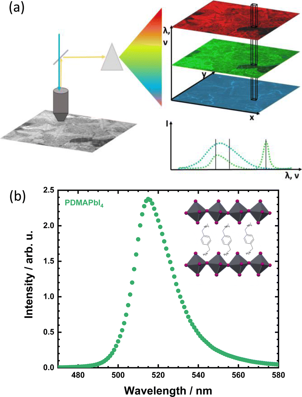 | ||
| Fig. 1 (a) Principle of hyperspectral PL and Raman imaging. A laser beam is directed through an objective to excite the sample (PL) or to be scattered. The signal is collected in reflection geometry, spectrally separated and generates a three-dimensional data cube with spatial x and y-, and a wavelength/wavenumber coordinate. This allows for selecting micrographs at distinct spectral positions (horizontal) or taking spectra at a fixed spatial location (vertical). (b) PL spectrum of a PDMAPbI4 thin film integrated over the entire field of view of a 20× objective in the hyperspectral microscope. Every circle corresponds to a micrograph. The insets illustrates the layered crystal structure with PDMA2+ spacer cations sandwiched between slabs of inorganic PbI octahedra. | ||
The Raman experiment generates an analogous data structure, where x and y coordinates define the location on the sample, and a third axis follows the wavenumber of the scattered signal. The Raman micrographs here were acquired via a confocal stage scanning approach. The sample is scanned point-by-point to give the x,y-coordinate by moving the sample's stage under a fixed beam.
Thin films of PDMAPbI4 were fabricated as reported before,16 and detailed in the Methods section. As is common for 2D HaPs based on lead and iodide,17,18 the material exhibits a relatively narrow luminescence peak around 515 nm in the green spectral region (Fig. 1(b)). Fig. 2 highlights the details of the PDMAPbI4 thin film emission at room temperature with high magnification (100×, 0.9 NA). When integrating the intensity over a broad spectral range (430–600 nm), a plethora of details can immediately be identified in the micrograph of Fig. 2(a): large grains in the range of tens of micrometres dominate the film and appear both in a relatively bright and a dark variant. Moreover, several grain boundaries appear bright, many grains show dark X-shapes, and a rich pattern of small bright spots and thin bright lines is noticeable. Fig. 2(a) is the result one would obtain from a conventional PL microscope without spectral resolution, highlighting how the analysis would be complicated by the sheer amount of features.
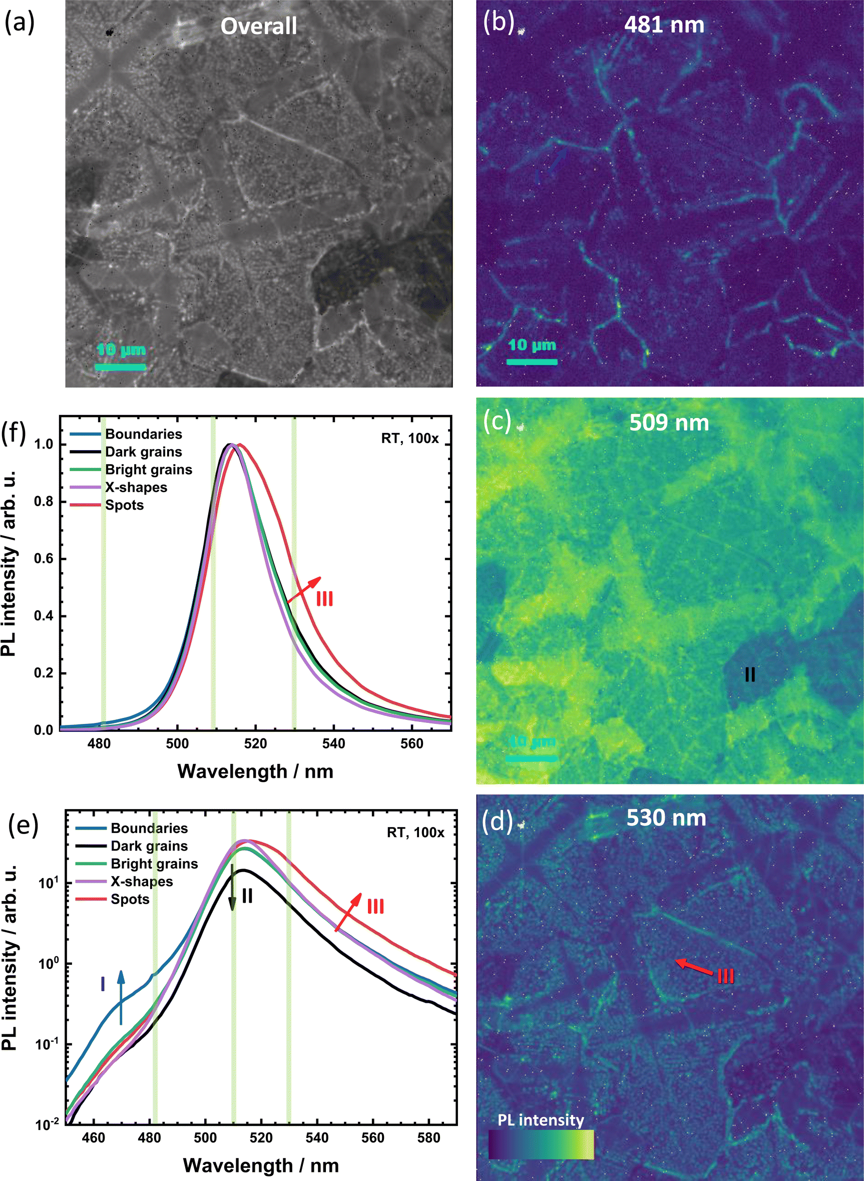 | ||
| Fig. 2 Hyperspectral PL microscopy at 100× magnification. (a) The overall intensity includes a large degree of heterogeneity and a plethora of features. Representative micrographs at 481 (b), 509 (c), and 530 nm (d) highlight how grain boundaries are bright at short wavelengths, and a fine pattern of bright spots emerges at long wavelengths in addition to the grain-to-grain difference around the main peak. Extracted (averaged) PL spectra for distinct features are shown in a semi-logarithmic plot (e) and normalised on a linear scale (f). Vertical lines indicate the position of the extracted images. The spectral differences of the grain boundaries, spot pattern, and dark grains are highlighted by I, II III, respectively. | ||
When considering the emission spectrally, it becomes apparent that most grain boundaries appear bright at short wavelengths, i.e. before the onset of the main emission peak, as illustrated in Fig. 2(b) with a micrograph at 481 nm. A larger field of view is provided in Fig. S1 (ESI†) underlining the ubiquity of this observation. The extracted average PL spectrum of these boundaries is given in Fig. 2(e) and (f) (Supplementary Note 1 and Fig. S2, ESI† for approach). As highlighted with the blue arrow and ‘I’, grain boundaries show an increased intensity over a relatively broad region – from at least 450 to approximately 490 nm – as the only spectral difference towards the rest of the film discussed in the following.
Around the main peak (509 nm) in Fig. 2(c), the above noted bright and dark grains dominate the overall view. The extracted spectra offer a clear intensity reduction of dark grains around the main peak (indicated ‘II’ in Fig. 2(e)) but identical shapes, as demonstrated by the normalised data in Fig. 2(f). Bright and dark grains also show the same trends at short wavelengths in Fig. 2(e). As a third feature, the 509 nm micrograph contains large and bright patches that form X-shapes. These regions exhibit a higher intensity around the main peak at 515 nm and a slightly narrower linewidth (magenta curve in Fig. 2(e) and (f)). Finally, we note an intricate array of narrow bright lines running through all three of the aforementioned regions.
By means of white light reflection and atomic force microscopy (AFM) (Fig. S3, ESI†), these thin lines can be identified as narrow trenches running as a fine net through the sample surface. AFM furthermore reveals the bright X-shapes to correspond to elevated regions of the sample, as highlighted in Fig. S4 (ESI†). These grains do no simply grow flatly, but include pyramid-like structures with ridges. Notably, we found similar features also in measurements performed by others,19 indicating that they are not unique to the processing conditions used here. The strong impact of both these aspects on the PL underlines how sample geometry and topography can profoundly affect macroscopically observable properties. In both cases, increased propensity of light outcoupling can straightforwardly explain why these structures appear brighter around the main peak.20 Furthermore, the presence of the trenches is a challenge when employing these films in applications where electrical shunts must be avoided – synthesis protocols will have to be optimised to fabricate continuous thin films.
Finally, two important observations can be made when considering wavelengths beyond the main peak at 515 nm shown in Fig. 2(d). Firstly, it is only at these longer wavelengths, where the above-mentioned fine pattern of bright spots emerges. Secondly, these spots seem to be present exclusively on bright grains. There are no bright spots on either the dark grains or the X-shapes. As shown in Fig. 2(e) and (f), the extracted spectra of these bright spots are red-shifted compared to the rest of the sample, and show a significantly increased intensity from 520 nm to the end of the measurement window at 590 nm (‘III’). In addition to the narrow trenches, the AFM micrograph in Fig. S3 (ESI†) shows a multitude of pinholes in the surface that seem responsible for these bright spots. We attribute this red-shift to the repeated absorption and re-emission undergone by waveguided photons that travel laterally (photon recycling) and subsequently become out-coupled at these pinholes or the trenches mentioned above.21,22
As noted above, these observations can generally also be made when considering a lower magnification. Importantly, though, an insufficient resolution of the small spots creates the impression of bright grains appearing uniformly bright at long wavelengths (Fig. S1, ESI†), which we here show not to be the case.
Taken together, the hyperspectral PL study at room temperature reveals a plethora of different features and different origins, which cannot be explained by a naive model of a single material comprising, for example, trap states and different exciton sub-states. In contrast, sample topography (ridges, trenches) and morphology (grain boundaries, grain-to-grain variation) are crucial.
Variation of the temperature can be used as a lever to modulate the photophysics and to offer further insight into the mechanisms at play. We thus performed the hyperspectral experiment over a range from 298 to 5 K. Fig. 3 shows selected micrographs for representative temperatures (250, 100, and 5 K) around the main emission peak (518–524 nm; panels (a) to (c)) and at short wavelengths (488–494 nm; panels (d) to (f)).
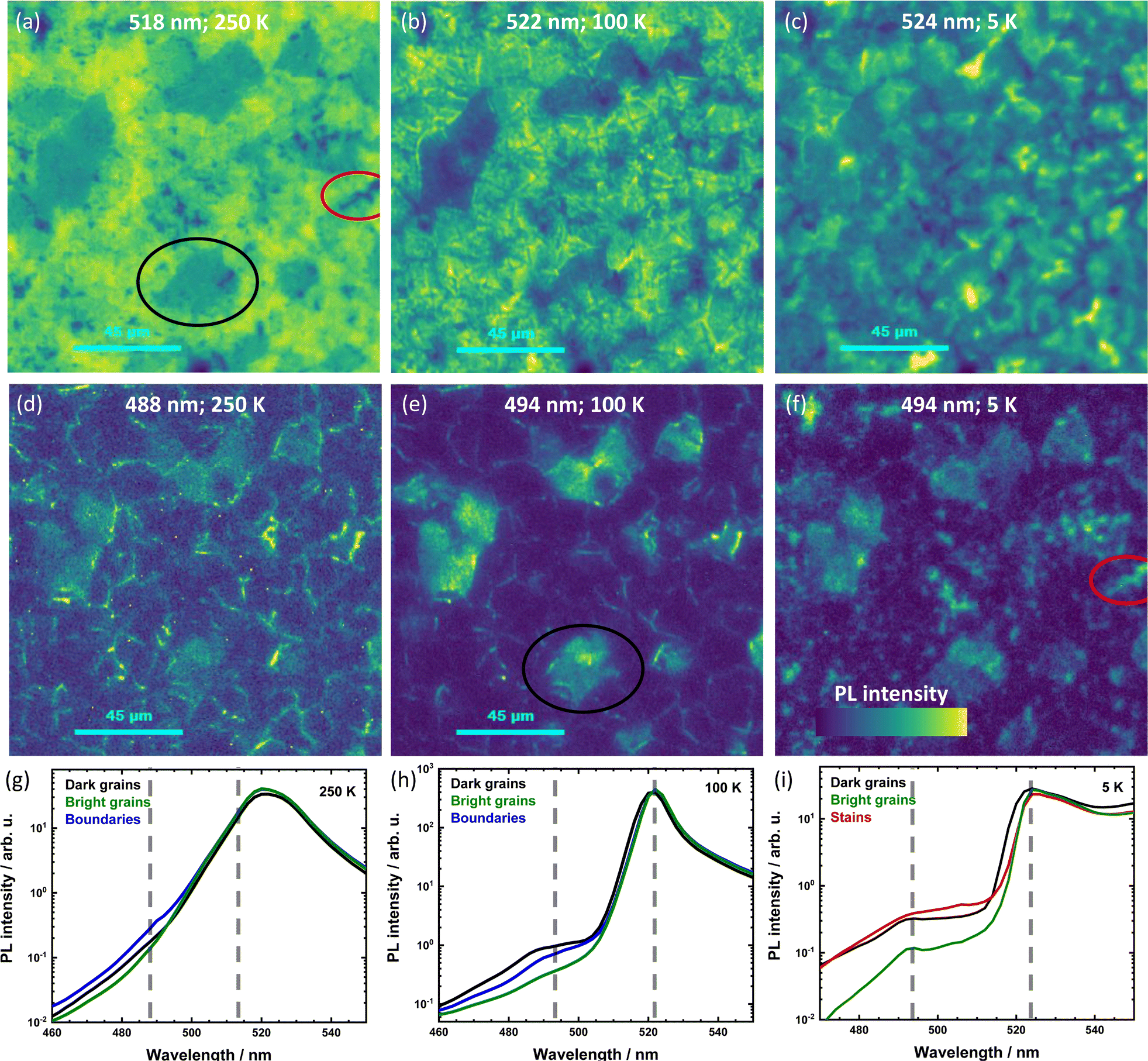 | ||
| Fig. 3 Temperature dependent hyperspectral PL microscopy for three selected temperatures (250, 100, 5 K) taken with a 20 × 0.45 NA objective. The intensity around the main emission peak (a–c) shows bright and dark (black circle) grains at elevated temperatures with a vanishing contrast at 5 K. At short wavelengths (d–f), the emission is dominated by dark grains and grain boundaries. The panels (g) to (i) show the extracted spectra for bright and dark grains (black circle), the boundaries, and the patches marked with a red circle. Vertical dashed lines indicate the location of the micrographs. | ||
At 250 K, the sample behaves similarly to the case at room temperature, i.e. a majority of grains emits relatively brightly around the main peak, but a number of grains appear significantly darker (a). However, the emission at shorter wavelengths (d) not only stems from grain boundaries anymore, but the micrographs contain distinct PL from those grains that are dark around the main peak. This contrast becomes obvious when extracting the spectra, shown in Fig. 3(g), where both the boundaries and the ‘dark grains’ exhibit a faint but distinct PL over a broad range of short wavelengths (for the approach consider Supplementary Note 1 and 2; also see linear plots in Fig. S5, ESI†).
This behaviour is retained down to temperatures of 30 K, for which the 100 K micrographs are given as examples: the image is dominated by bright grains around the main peak, and includes dark grains that appear bright at short wavelengths (Fig. 3(b)). Increasingly, the emission of these ‘dark grains’ dominates at short wavelengths, but the boundaries remain distinctly visible (e). The extracted spectra in Fig. 3(h) (or Fig. S5, ESI†) show the reduced linewidth expected from a reduction in thermal broadening, as well as a slight blue-shift of the main peak of ‘dark grains’, similarly observed before.16 The short wavelength emission, on the other hand, remains broad and spans the measured window from 460 to 505 nm.
At 5 K, finally, the intensity around the main peak is similar for the bright and the dark grains (Fig. 3(c), but the dark grains exhibit the pronounced blue-shifted spectrum, as can be seen in (i) (more pronounced in Fig. S5 and S6, ESI†). Moreover, whereas the dark grains’ emission at short wavelengths is retained, that of grain boundaries is now quenched (panel (f)). The extracted spectra at 5 K in panel (i) also exhibit a faint, but distinct, peak around 493 nm. For related materials, such narrow peaks at short wavelengths have previously been attributed to recombination from hot excitons,23,24 but it also coincides precisely with the emission expected from PbI2,25 to which it was previously ascribed in PDMAPbI4 films.26 Given the strongly localised origin of this emission, shown in Fig. S7 (ESI†), the attribution to PbI2 instead of hot excitons is consistent.
In addition to the broad contribution from the dark grains and the narrow peak of PbI2 at 493 nm, the 5 K emission at short wavelengths exhibits smaller patches, which can be already identified at elevated temperatures (red circles in Fig. 3(a) and (f)). These patches were only observed for the sample used in the temperature-dependent experiment and are likely due to an impurity phase on the surface or perturbed cystallisation of the film.
Concluding the insights from the hyperspectral PL experiments, we find that PDMAPbI4 thin films offer a highly complex and heterogeneous picture of PL spectra. In addition to exhibiting an intricate network of trenches, pinholes, and bright grain boundaries, approximately a third of the micron-sized crystallites are what we described as ‘dark grains’. These crystallites show a fainter room temperature PL and they not only exhibit a blue-shifted onset of the main peak upon cooling, but distinct short-wavelength luminescence.
We note that PDMAPbI4 was previously reported to form a hydrated structure upon exposure to humid air.19 Although our samples were fabricated and measured under inert atmosphere, such hydration could give rise to a strong grain-to-grain variation. Furthermore, x-ray diffraction patterns were previously invoked to claim that PDMAPbI4 thin films contain both crystallites with their layers stacked in out-of-plane and in in-plane direction.19 In principle, this could also be responsible for differences in PL spectra.
We thus studied the orientation of the crystalline domains within the thin film via grazing incidence wide angle x-ray scattering (GIWAXS), as discussed in the ESI† (Supplementary Note 3 and Fig. S8, S9). The GIWAXS patterns taken at different incident angles (i.e. different penetration depth) all show that the material crystallized into domains with a preferential out-of-plane stacking orientation. However, crystallites with in-plane stacking, as well as other randomly distributed orientations, are also present, especially within the bulk of the film.
Using these insights for microscopic experiments, we note that reflected light microscopy reveals a stark contrast between different grains when a cross-polarised configuration is employed (Fig. S10, ESI†). Similarly, transmitted white light microscopy also shows clear birefringence when crossed polarisers are introduced into the beam path – both highlighting the strong grain-to-grain variation of optical properties. Whereas direct comparison to wide-field and confocal PL maps reveal a certain degree of similarity (Fig. S11, ESI†), it is difficult to differentiate and to establish direct correlations between morphological effects, grain orientation, chemical composition, and optical properties using these techniques.
Raman spectro-microscopy, however, can be used as a non-invasive tool to provide information on grain orientation and material composition, as we and others have recently shown for Ruddlesden–Popper perovskites.27–29 The unpolarised Raman spectrum of PDMAPbI4 shows three dominant Raman- active modes located at 28, and 46, and 61 cm−1, as well as minor peaks at 20, 38, 99, and 110 cm−1 (Fig. S12, ESI†). These peaks occur at similar frequencies to those previously observed in thin films of PEA2PbI4. Krahne and coworkers recently assigned similar peaks at low frequency in (PEA)2PbBr4 to vibrational modes relating to the bending and twisting of Pb–Br bonds, and in-plane scissoring of Br–Pb–Br bonds.30 Owing to the anisotropy of these modes, the Raman spectrum is highly sensitive to the crystallographic orientation in these layered materials. These modes can thus be used as a sensitive probe to map the in-plane orientation of 2D HaPs. In particular, the ratio between the 40 and 56 cm−1 peaks provides good contrast between grains with different in-plane crystallographic orientations.27 To investigate the crystallographic orientation of grains in the PDMAPbI4 films, we adopt a similar approach here.
Fig. 4(a) shows the average linearly polarised Raman spectra obtained from the sample area depicted in the white light micrograph of Fig. 4(b) (50× 0.5 NA), measured in the configurations Z(XX)![[Z with combining macron]](https://www.rsc.org/images/entities/i_char_005a_0304.gif) and Z(YX) in the Porto notation. The relative magnitude of the observed Raman modes provides a means of mapping differences in orientation of these systems (Supplementary Note 3, ESI†). In particular, the intensity ratio of the 46 to 61 cm−1 peaks (46/61) in the Z(YX) provides a stark contrast between adjacent grains. Despite the lack of discernible grain boundaries in the white light image, the ratio map clearly reproduces individual grains with sizes up to several tens of micrometres (exemplary cases are indicated by arrows), as well as a cluster of smaller grains (encircled) in the lower left part of the map. In addition to chemical analysis, Raman microscopy thus also serves as a powerful tool for the microstructural analysis of emerging DJ perovskites. Importantly, there is no correlation between darker and brighter regions of the white light image and the (46/61) ratio map. In other words, although we clearly study a region that contains both bright and dark grains (under white light or PL), these are all stacked in out-of-plane direction and their axes are rotated in-plane; dark grains are thus not a consequence of a minority phase of in-plane stacked grains. Moreover, the ratio map does not exhibit clear features related to the aforementioned X-shapes, further supporting that these are caused by the surface topography rather than by a different orientation. We note that it is possible to determine the absolute orientation of the grains, as recently performed by Toda et al. for (BA)2PbI4,29 but full knowledge of the Raman tensor of PDMAPbI4 would be required, which goes beyond the scope of the current work.
and Z(YX) in the Porto notation. The relative magnitude of the observed Raman modes provides a means of mapping differences in orientation of these systems (Supplementary Note 3, ESI†). In particular, the intensity ratio of the 46 to 61 cm−1 peaks (46/61) in the Z(YX) provides a stark contrast between adjacent grains. Despite the lack of discernible grain boundaries in the white light image, the ratio map clearly reproduces individual grains with sizes up to several tens of micrometres (exemplary cases are indicated by arrows), as well as a cluster of smaller grains (encircled) in the lower left part of the map. In addition to chemical analysis, Raman microscopy thus also serves as a powerful tool for the microstructural analysis of emerging DJ perovskites. Importantly, there is no correlation between darker and brighter regions of the white light image and the (46/61) ratio map. In other words, although we clearly study a region that contains both bright and dark grains (under white light or PL), these are all stacked in out-of-plane direction and their axes are rotated in-plane; dark grains are thus not a consequence of a minority phase of in-plane stacked grains. Moreover, the ratio map does not exhibit clear features related to the aforementioned X-shapes, further supporting that these are caused by the surface topography rather than by a different orientation. We note that it is possible to determine the absolute orientation of the grains, as recently performed by Toda et al. for (BA)2PbI4,29 but full knowledge of the Raman tensor of PDMAPbI4 would be required, which goes beyond the scope of the current work.
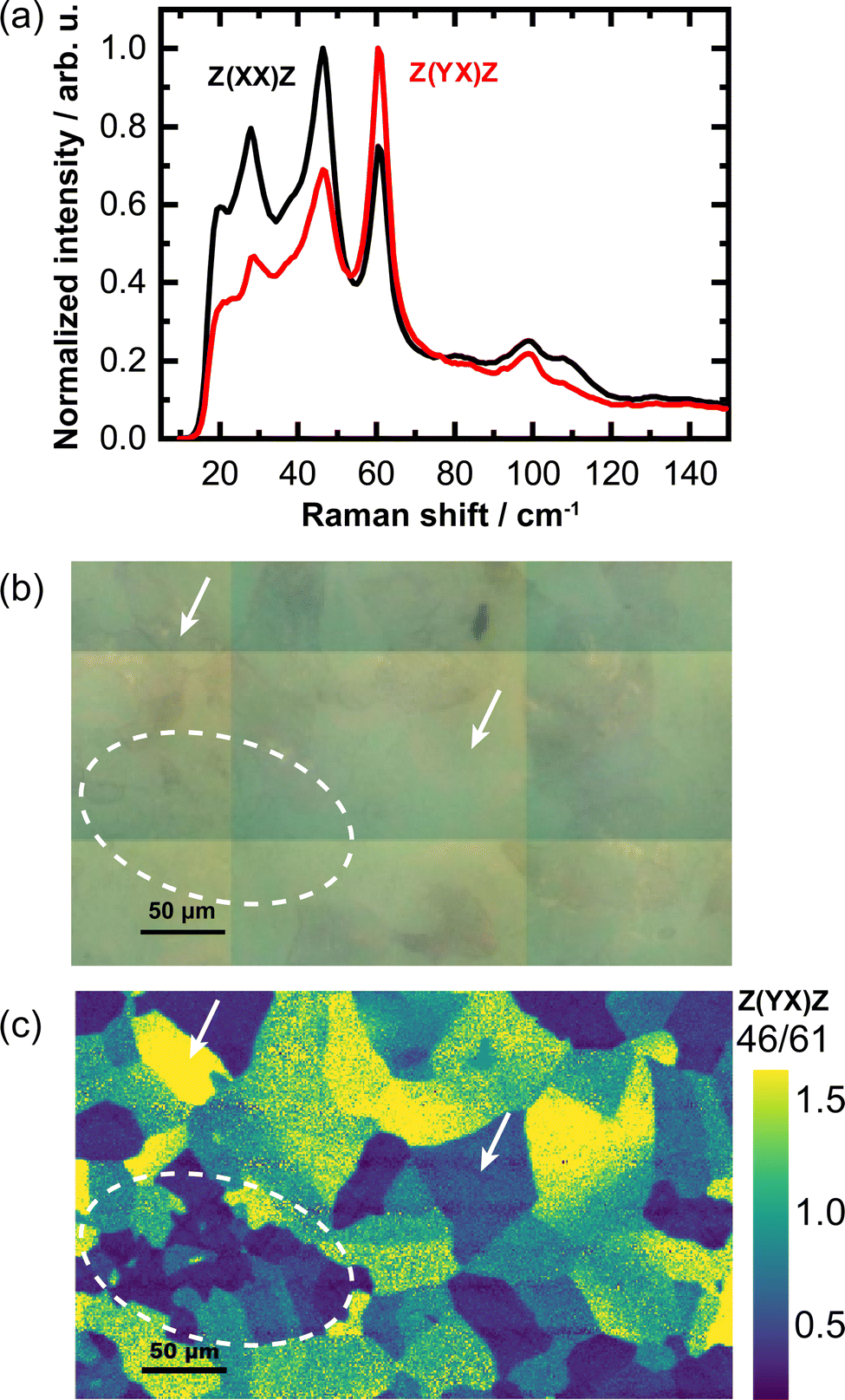 | ||
| Fig. 4 (a) Average polarised Raman spectra of PDMAPbI4 measured in the Z(XX) and Z(YX) configuration, where the terms inside the brackets indicate the polarisation direction of the incident and detected light, respectively. (b) White light micrograph of the area on which Raman maps were acquired. (c) False colour map showing the ratio of the intensity of the 46 cm−1 peak over the 61 cm−1 peak for the Z(YX) polarisation. | ||
Monitoring large areas of the film, we generally encounter the same impression. Fig. 5(a) shows an intensity map of the 61 cm−1 mode. Principal component analysis on the data set reveals that most grains can be classified as being composed of one of two main principal components, PC1 and PC2 or a combination thereof (Fig. S13, ESI†), where PC1 is characterised by a strong intensity of the 61 cm−1 mode and PC2 by a strong intensity at 45 cm−1. However, we also observe a small sub-set of crystallites that exhibit only minor Raman scattering intensities and provide an exemplary case of such a grain in the top left corner of the map (see arrow). Such grains offer a very low score for both principal components.
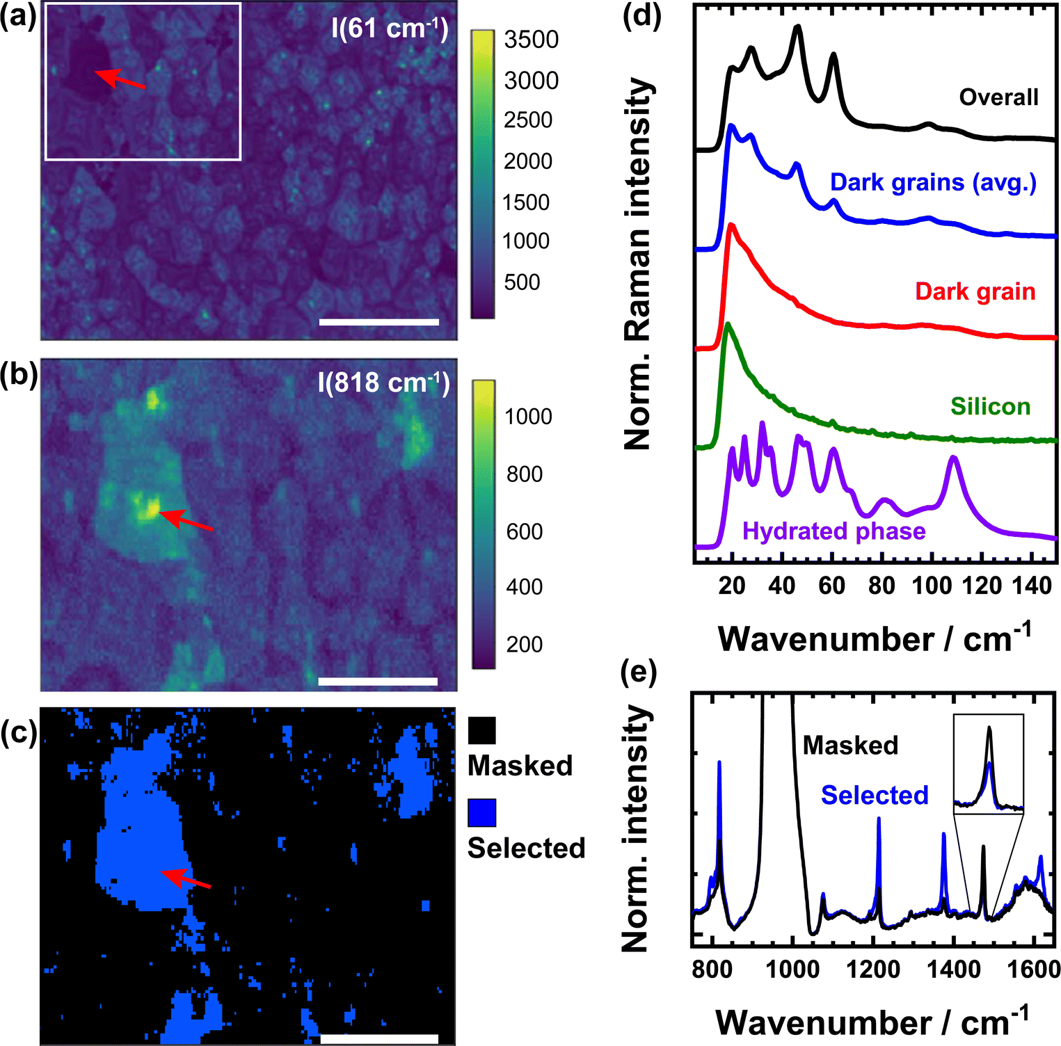 | ||
| Fig. 5 Unpolarised Raman intensity maps of the 61 cm−1 and (b) 818 cm−1 mode. The arrow indicates the deviating grain discussed in the main text, while the rectangular box indicates the area from which the high wavenumber intensity map in (b) was acquired. (c) Example of a mask used to select Raman spectra exclusively from the diverging grains; in this case only data for which the Raman intensity of the 818 cm−1 vibration exceeds 400 counts was selected while all other data was masked. A similar mask was used to select the dark grains in (a). Scale bars are 100 μm in (a) and 50 μm in (b) and (c). (d) Comparison between the normalised unpolarised Raman spectra of PDMAPbI4 (black) and the average spectra obtained from the dark grains in (a) (blue). In the extreme case, the Raman spectra obtained from a single point on the dark grain (red) hardly exhibits any peaks from PDMAPbI4. For reference the scattering from a bare silicon spectra (green) and the hydrated phase of PDMAPbI4 (purple) are reported as well. (e) Raman spectra obtained from the selected and masked areas in (c), spectra are normalised to their silicon baseline. The inset highlights the inverse intensity trend of the 1474 cm−1 mode, as compared the other high-wavenumber vibrations. | ||
Interestingly, we find that a reduced intensity in the low-energy part of the Raman spectrum coincides with an increased intensity for most of the high-energy vibrational modes associated with the organic cation, as depicted in the intensity map of the 818 cm−1 mode in Fig. 5(b). The normalised Raman spectra obtained from these selected grains (Fig. 5(c)) are compared to the average Raman spectrum of the entire map in Fig. 5(d) and (e) for the low and the high wavenumber part of the spectrum, respectively. This comparison highlights that the selected grains do not exhibit different peaks from the average PDMAPbI4 spectrum, but mainly differ in terms of their overall intensity. Whereas the low wavenumber Raman spectra from typical grains are dominated by either the 46 or 61 cm−1 mode, the average spectrum of the selected grains instead shows a continuously increasing background signal towards low wavenumbers that is cut off by the filter at 15 cm−1 with peaks of the DJ perovskite superimposed. In some extreme cases hardly any peaks from PDMAPbI4 can be observed and the spectrum closely resembles that of light scattered off a bare silicon substrate. At the same time, the high wavenumber peaks associated with vibrational modes of the PDMA2+ cation (Fig. S14, ESI†) show an increased intensity for the selected grains, as can be seen in Fig. 5(e). This holds true for all vibrational modes in the range from 600 to 1100 cm−1, except for the peak near 1500 cm−1, which shows an inverse trend.
We propose that these grains correspond to the in-plane oriented sub-population, where the inorganic layers are perpendicular to the substrate. In such a case, the k vector of the incident polarised laser light is orthogonal to the long axis of the unit cell and the reduced effective cross section of the inorganic planes could reduce scattering from low energy Raman modes. Moreover, as some of these modes are predominantly associated with in-plane motion of the Pb–I bonds, the electric field of the incident light might not be able to efficiently drive these vibrations owing to symmetry consideration. Scattering from the organic cations on the other hand might be favoured in such a configuration.
Alternative explanations, such as a locally decreased film thickness, can be excluded based on the strong presence of organic modes, and we furthermore do not find any supporting evidence from the morphological characterisations through reflected light microscopy, AFM or SEM measurement (Fig. S16, ESI†) for such an assumption. Similarly, we can exclude grains of different composition, such as large clusters of PbI2 or the hydrated phase19 based on the absence of any changes in the Raman spectra at low energy (Fig. 5(d)).
Taken together, our experimental results suggest a picture as summarised in Fig. 6. Micrometre-sized crystallites predominantly form with their layers stacked in out-of-plane direction and rotational disorder in the sample plane. A small minority forms with different orientation including in-plane and arbitrary tilt alignment, as suggested by both Raman spectro-microscopy and GIWAXS. Grain boundaries act as distinct sources of high-energy emission – increasingly pronounced at low temperature. Similarly, dark grains exhibit high-energy luminescence that brightens upon cooling – either due to suppression of non-radiative recombination or due to the suppression of excitation transfer towards lower states. Since neither the Raman nor the GIWAXS experiments indicate the formation of secondary crystalline phases, we rule out that these dark grains are a different material. Still, as evidenced by the presence of nanoscale PbI2, it could be possible that small amounts of a wide band gap material forms on the surface of these dark grains. Running through the entire film is an intricate pattern of trenches that might form to relieve stress during the cooling stage after film deposition.
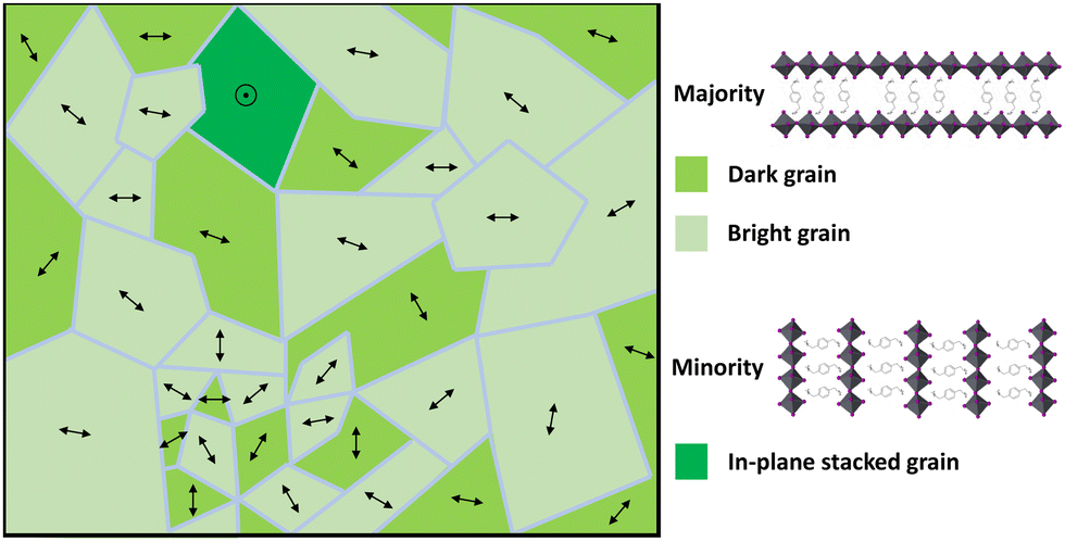 | ||
| Fig. 6 Schematic of the PDMAPbI4 thin film microstructure. Micro-metre sized crystallites predominantly form with layers parallel to the substrate, i.e. stacked in out-of-plane direction. These crystallites are rotationally disordered around the stacking direction (indicated by the double-arrows) and can be either bright or dark. A minor sub-population of crystallites forms with their layers perpendicular to the substrate, i.e. stacked in in-plane direction. | ||
3 Conclusions
We performed a combined high-resolution hyperspectral microscopy and Raman microscopy investigation of the Dion–Jacobson perovskite PDMAPbI4. Spin-cast films of PDMAPbI4 posses a diverse morphology and strong variations in the optical properties on a microscopic scale. Grain boundaries, grain interior and microstructural features are shown to result in distinct photoluminescence spectra that evolve differently upon temperature variation. Raman microscopy and x-ray scattering furthermore reveal that a majority of grains to grow with out-of-plane stacking direction, whilst a small minority forms with in-plane stacked layers and random orientation. Our results highlight that the presence of bight and dark grains is neither due to different crystallite orientation nor due to the presence of a secondary phase.As our study revealed, fabrication protocols for PDMAPbI4 will have to be optimisied further in order to create a uniform, crack-free, and flat thin film, when aiming at applications in optoelectronic devices. At the same time, the origin of the heterogeneous formation of defects remains a key unknown that warrants further study.
4 Experimental
Sample preparation
Thin films of PDMAPbI4 were deposited on quartz substrates for PL experiments, on glass for GIWAXS, and on silicon for Raman experimentation. Precursor solutions were obtained through dissolving lead iodide and 1,4-phenylenedimethanammoniumdiiodide (PDMAI2) in a mixed solvent composed of n,n-dimethylformamide (DMF) and dimethyl sulfoxide (DMSO), at 4![[thin space (1/6-em)]](https://www.rsc.org/images/entities/char_2009.gif) :1 volume ratio. In a typical experiment, 156.8 mg PDMAI2 were mixed with 184.6 mg PbI2 in 0.4 mL DMF and 0.1 mL DMSO.
:1 volume ratio. In a typical experiment, 156.8 mg PDMAI2 were mixed with 184.6 mg PbI2 in 0.4 mL DMF and 0.1 mL DMSO.
Prior to deposition, the substrates are ultrasonically cleaned through a series of four baths of detergent solution, deionised water, acetone, and isopropanol. At each step, sonication occurred for two periods of 10 minutes, with the solvent being replaced after the first leg. Subsequently, the substrates are dried for 10 minutes at 140 °C and subjected to an ultraviolet ozone treatment for 20 minutes before immediately being transferred into a nitrogen-filled glovebox for film deposition. The perovskite film was deposited using a single-step spin programme antisolvent method. The spinning speed is set to 5000 rpm with a duration of 50 seconds; the antisolvent (toluene) was applied perpendicular to the substrate 35 seconds into the spin programme. Upon completion, the films were immediately transferred to a hot plate to be annealed at 120 °C for 20 minutes. The remaining solvent quickly evaporated upon heating leading to a rapid crystallization of the perovskite and color change to bright red/yellow for the tin and lead-based compound, respectively.
Hyperspectral PL microscopy
Wide-field, hyperspectral microscopy measurements were carried out using a Photon etc. IMA system. Measurements were performed either with an Olympus LMPlanFL N 100× (NA = 0.8) or a Nikon TU Plan Fluor 20× (NA = 0.45) objective lens. The sample was kept in air for the room temperature measurement and under vacuum for the temperature-dependent experiment. Excitation occurred with a 405 nm continuous wave laser (unpolarised), which was filtered out by a dichroic longpass for the detection. A 50 W halogen lamp was used for reflection measurements. The emitted/reflected light from the sample was incident on a volume Bragg grating, which splits the light spectrally onto a CCD camera. The detector was a 1040 × 1392 resolution silicon CCD camera kept at 0 °C with a thermoelectric cooler and has an operational wavelength range of 400–1000 nm. By scanning the angle of the grating relative to the incident light, the spectrum of light coming from each point on the sample could be obtained.For the temperature-dependent experiment, the sample was fixed with silver paste to the cold finger of an Oxford HiRes cryostat cooled with liquid helium. The cryostat was attached to the microscope with a self-made holder allowing for focus correction. The sample was held at the set temperature for 15 minutes prior to every measurement.
Confocal Raman microscopy
Raman spectroscopy was performed using an InVia Qontor confocal Raman microscope (Renishaw, UK). A Leica 50× N Plan objective (0.50 NA) was used to focus the output of a 785 nm continuous wave laser onto the sample. The excitation power was controlled using a set of neutral density filters. The scattered light was collected by the same objective and passed through a Renishaw low wavenumber Eclipse filter to eliminate Rayleigh scattered light and allow only Raman scattered with a Raman shift larger than 15 cm−1 to pass. The Raman scattered light was then passed through a pinhole and subsequently dispersed by a 1800 lines per millimetre grating and imaged by a silicon CCD camera. Maps were recorded at an excitation power of 5.5 mW and a pixel dwell time of 2 s. All Raman measurements were performed under ambient conditions.Reflected light microscopy
Reflected white-light micrographs were obtained on an Olympus BX51M microscope. A linear polarizer and analyzer were inserted in the optical beam path in a cross polarized configuration for the polarisation image.Wide-field PL and transmission white light microscopy
An inverted Nikon Ti–e microscope was used to capture fluoresence and transmitted light micrographs. Wide-field fluoresecence images were captured upon excitation by the blue line of a mercury vapour lamp and imaged on an Andor Luca EMCCD. Transmitted white-light micographs were obtained using the same detection scheme, with polarisers inserted the optical beam path before and after the sample plane for polarisation resolved imaging. Depending on the required resolution, either a 40× ELWD objective or an oil-immersion 100× objective was used.Electron microscopy
An FEI Nova Nano SEM 650 instrument equipped with a gaseous analytical detector (GAD) was used to obtain scanning electron micrographs of the thin film in its true native state.Atom force microscopy
Atomic force micrographs were recorded using a Bruker NanoScope V instrument operated in the ScanAsyst tapping mode.GIWAXS
measurements were performed at the multipurpose instrument for nanostructure analysis (MINA) instrument at the University of Groningen. The instrument is built on a Cu rotating anode providing an X-ray beam with wavelength λ = 0.15413 nm. GIWAXS patterns were acquired using a Pilatus 300 K detector from Dectrix with pixel size 0.172 × 0.172 mm. The detector was placed 83 mm away from the sample. All the necessary corrections to the GIWAXS patterns were applied to retrieve the missing wedge-corrected patterns, taking into account the Ewald sphere curvature effect. The position of the direct beam and the probed angular range were calibrated using known positions from diffraction peaks from a standard Silver Behenate sample. The patterns are reported as a function of the parallel qr and vertical qz scattering vectors.Author contributions
SK conceived the study, performed the hyperspectral microscopy, and initial Raman experiments. HD performed follow-up Raman studies, AFM, and SEM experiments. KF supported the temperature-dependent experiments. AJR fabricated the samples. GHtB supported the SEM experiments, GP performed and analysed the GIWAXS studies. SDS and MAL supervised the work in Cambridge and Groningen, respectively. SK and HD wrote the first draft, all authors contributed to the final version.Conflicts of interest
SDS is a co-founder of Swift Solar.Acknowledgements
Arjen Kamp and Teodor Zaharia are thanked for technical support. SK is grateful for a postdoctoral fellowship (91793256) from the German Academic Foreign Service (DAAD). KF acknowledges a George and Lilian Schiff Studentship, Winton Studentship, the Engineering and Physical Sciences Research Council (EPSRC) studentship, Cambridge Trust Scholarship, and Robert Gardiner Scholarship. This work was financed through the Materials for Sustainability (Mat4Sus) programme (739.017.005) of the Netherlands Organisation for Scientific Research (NWO). The work has received funding from the European Research Council under the European Union's Horizon 2020 research and innovation programme (HYPERION, grant agreement no. 756962). The authors acknowledge the EPSRC (EP/R023980/1).References
- S. D. Stranks and H. J. Snaith, Nat. Nanotechnol., 2015, 10, 391–402 CrossRef CAS PubMed.
- K. Ji, M. Anaya, A. Abfalterer and S. D. Stranks, Adv. Opt. Mater., 2021, 9, 2002128 CrossRef CAS.
- X. Wei, T. Tanaka, Y. Yomogida, N. Sato, R. Saito and H. Kataura, Nat. Commun., 2016, 7, 12899 CrossRef CAS PubMed.
- A. K. Jena, A. Kulkarni and T. Miyasaka, Chem. Rev., 2019, 119, 3036–3103 CrossRef CAS PubMed.
- S. Feldmann, S. Macpherson, S. P. Senanayak, M. Abdi-Jalebi, J. P. H. Rivett, G. Nan, G. D. Tainter, T. A. S. Doherty, K. Frohna, E. Ringe, R. H. Friend, H. Sirringhaus, M. Saliba, D. Beljonne, S. D. Stranks and F. Deschler, Nat. Photonics, 2020, 14, 123–128 CrossRef CAS.
- K. Frohna, M. Anaya, S. Macpherson, J. Sung, T. A. S. Doherty, Y.-H. Chiang, A. J. Winchester, K. W. P. Orr, J. E. Parker, P. D. Quinn, K. M. Dani, A. Rao and S. D. Stranks, Nat. Nanotechnol., 2022, 17, 190–196 CrossRef CAS PubMed.
- T. A. S. Doherty, S. Nagane, D. J. Kubicki, Y.-K. Jung, D. N. Johnstone, A. N. Iqbal, D. Guo, K. Frohna, M. Danaie, E. M. Tennyson, S. Macpherson, A. Abfalterer, M. Anaya, Y.-H. Chiang, P. Crout, F. S. Ruggeri, S. Collins, C. P. Grey, A. Walsh, P. A. Midgley and S. D. Stranks, Science, 2021, 374, 1598–1605 CrossRef CAS PubMed.
- J. Ferrer Orri, T. A. Doherty, D. Johnstone, S. M. Collins, H. Simons, P. A. Midgley, C. Ducati and S. D. Stranks, Adv. Mater., 2022, 34, 2200383 CrossRef CAS PubMed.
- T. A. S. Doherty, A. J. Winchester, S. Macpherson, D. N. Johnstone, V. Pareek, E. M. Tennyson, S. Kosar, F. U. Kosasih, M. Anaya, M. Abdi-Jalebi, Z. Andaji-Garmaroudi, E. L. Wong, J. Madéo, Y.-H. Chiang, J.-S. Park, Y.-K. Jung, C. E. Petoukhoff, G. Divitini, M. K. L. Man, C. Ducati, A. Walsh, P. A. Midgley, K. M. Dani and S. D. Stranks, Nature, 2020, 580, 360–366 CrossRef CAS PubMed.
- S. D. Stranks, Matter, 2021, 4, 3852–3866 CrossRef CAS.
- T. Ishihara, J. Takahashi and T. Goto, Solid State Commun., 1989, 69, 933–936 CrossRef CAS.
- J.-C. Blancon, J. Even, C. C. Stoumpos, M. G. Kanatzidis and A. D. Mohite, Nat. Nanotechnol., 2020, 15, 969–985 CrossRef CAS PubMed.
- L. Mao, W. Ke, L. Pedesseau, Y. Wu, C. Katan, J. Even, M. R. Wasielewski, C. C. Stoumpos and M. G. Kanatzidis, J. Am. Chem. Soc., 2018, 140, 3775–3783 CrossRef CAS PubMed.
- X. Li, W. Ke, B. Traoré, P. Guo, I. Hadar, M. Kepenekian, J. Even, C. Katan, C. C. Stoumpos, R. D. Schaller and M. G. Kanatzidis, J. Am. Chem. Soc., 2019, 141, 12880–12890 CrossRef CAS PubMed.
- Y. Li, J. V. Milić, A. Ummadisingu, J.-Y. Seo, J.-H. Im, H.-S. Kim, Y. Liu, M. I. Dar, S. M. Zakeeruddin, P. Wang, A. Hagfeldt and M. Grätzel, Nano Lett., 2019, 19, 150–157 CrossRef CAS PubMed.
- S. Kahmann, H. Duim, A. J. Rommens, E. K. Tekelenburg, S. Shao and M. A. Loi, Adv. Opt. Mater., 2021, 9, 2100892 CrossRef CAS.
- S. Kahmann, H. Duim, H.-H. Fang, M. Dyksik, S. Adjokatse, M. Rivera Medina, M. Pitaro, P. Plochocka and M. A. Loi, Adv. Funct. Mater., 2021, 31, 2103778 CrossRef CAS.
- E. I. Marchenko, S. A. Fateev, A. A. Petrov, V. V. Korolev, A. Mitrofanov, A. V. Petrov, E. A. Goodilin and A. B. Tarasov, Chem. Mater., 2020, 32, 7383–7388 CrossRef CAS.
- A. Duičinskas, G. Y. Kim, D. Moia, A. Senocrate, Y.-R. Wang, M. A. Hope, A. Mishra, D. J. Kubicki, M. Siczek, W. Bury, T. Schneeberger, L. Emsley, J. V. Milić, J. Maier and M. Grätzel, ACS Energy Lett, 2021, 6, 337–344 CrossRef.
- J. M. Richter, M. Abdi-Jalebi, A. Sadhanala, M. Tabachnyk, J. P. Rivett, L. M. Pazos-Outón, K. C. Gödel, M. Price, F. Deschler and R. H. Friend, Nat. Commun., 2016, 7, 13941 CrossRef CAS PubMed.
- C. Cho, B. Zhao, G. D. Tainter, J. Y. Lee, R. H. Friend, D. Di, F. Deschler and N. C. Greenham, Nat. Commun., 2020, 11, 1–8 CrossRef PubMed.
- C. Cho, Y.-W. Jang, S. Lee, Y. Vaynzof, M. Choi, J. H. Noh and K. Leo, Sci. Adv., 2021, 7, 1–9 Search PubMed.
- D. B. Straus, S. Hurtado Parra, N. Iotov, J. Gebhardt, A. M. Rappe, J. E. Subotnik, J. M. Kikkawa and C. R. Kagan, J. Am. Chem. Soc., 2016, 138, 13798–13801 CrossRef CAS PubMed.
- S. Kahmann, E. K. Tekelenburg, H. Duim, M. E. Kamminga and M. A. Loi, Nat. Commun., 2020, 11, 2344 CrossRef CAS PubMed.
- E. K. Tekelenburg, S. Kahmann, M. E. Kamminga, G. R. Blake and M. A. Loi, Adv. Opt. Mater., 2021, 2001647 CrossRef CAS.
- M. Kaiser, Y. Li, J. Schwenzer, M. Jakoby, I. Allegro, M. Gerhard, M. Koch, A. Ducinskas, B. S. Richards, M. Graetzel, J. V. Milić, U. W. Paetzold and I. A. Howard, J. Appl. Phys., 2021, 129, 123101 CrossRef CAS.
- H. Duim, G. H. Ten Brink, S. Adjokatse, R. de Kloe, B. J. Kooi, G. Portale and M. A. Loi, Small Struct., 2020, 1, 2000074 CrossRef.
- S. Toda, N. Yanagita, E. Jokar, E. W.-G. Diau and S. Shigeto, J. Phys. Chem. Lett., 2020, 11, 3871–3876 CrossRef CAS PubMed.
- S. Toda, E. W.-G. Diau and S. Shigeto, J. Phys. Chem. C, 2021, 125, 27996–28003 CrossRef CAS.
- B. Dhanabalan, Y.-C. Leng, G. Biffi, M.-L. Lin, P.-H. Tan, I. Infante, L. Manna, M. P. Arciniegas and R. Krahne, ACS Nano, 2020, 14, 4689–4697 CrossRef CAS PubMed.
Footnotes |
| † Electronic supplementary information (ESI) available. See DOI: https://doi.org/10.1039/d2tc04406d |
| ‡ These authors contributed equally to this work. |
| This journal is © The Royal Society of Chemistry 2022 |