Balancing the performance and stability of organic photodiodes with all-polymer active layers

Xiaodong Huang a, Zhenmin Zhao *a, Sein Chung b, Kilwon Cho b, Jie Lv c, Shirong Lu c and Zhipeng Kan a
aSchool of Physical Science and Technology, Guangxi University, Nanning, 530004, China. E-mail: 2007401038@st.gxu.edu.cn
bDepartment of Chemical Engineering, Pohang University of Science and Technology, Pohang 37673, South Korea
cChongqing Institute of Green and Intelligent Technology, Chinese Academy of Sciences, Chongqing, 400714, China

Received 30th September 2022 , Accepted 24th October 2022

First published on 24th October 2022


Abstract

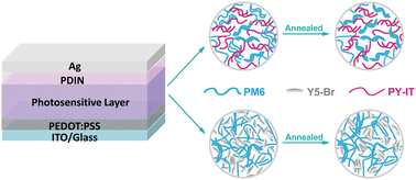
Organic photodiodes (OPDs) have emerged as a potential alternative for inorganic photodiodes in light-detection technology due to their unique properties such as lightweight, flexibility, and tunable absorption range. However, the stability of OPDs is one of the main issues preventing the commercialization of OPDs. Herein, we performed a detailed characterization study of OPDs composed of all-polymer and polymer donors/small molecular acceptors to evaluate the detectivity and stability of devices. The small molecule acceptor Y5-Br and its polymerized counterpart PY-IT were selected to minimize the energy and absorption differences and paired with PM6. We found that the Y5-Br based device exhibited a higher detectivity and a lower dark current density due to the lesser extent of the trap density, whereas the PY-IT based device demonstrated a faster response time and impressive thermal/electrical stability. In addition, the analysis of the photosensitive layer morphology reveals that the all-polymer films showed remarkable thermal tolerance. In contrast, the thermal treatment resulted in apparent polymer and small molecule aggregations in the polymer–small molecule counterpart, leading to large scale phase segregations. Our findings suggest that the all-polymer composition is an efficient strategy to improve the stability of OPDs and provide a useful guidance for the commercial application of OPDs in the future.


Introduction

Photodetectors (PDs) are vital constituents in devices for the applications of environmental monitoring,1 industrial automatic control,2 optical sensors in optical control switches, etc.3–6 Due to the mature manufacturing process, high performance, perfect stability and feasible integration with modern electronic devices, PDs composed of inorganic semiconductors are still dominating the photodetection technology.7,8 However, their rigid structures and limited area scaling at low cost constrain their use in some emerging applications.9 Therefore, it is necessary to find the replacements with low manufacturing cost, high detection performance and good stability. In addition, the future application of PDs in daily activity monitoring is broad, requiring the ability of PDs to be attached to flexible and curved soft surfaces.10–12 Fuentes-Hernandez et al. reported that an appropriate selection of the organic semiconductor and electrode materials can improve the diode characteristics.13 In their work, P3HT:ICBA was adopted as the photosensitive layer, MoOx was used as the hole transporting layer, and PEIE was chosen as the electron transporting layer. With such a device geometry, organic photodetectors (OPDs) outperform the low-noise silicon photodiodes in all metrics, except the response time. In particular, they can detect low light levels under a low noise. Furthermore, large-area OPDs with customized shapes on flexible substrates with Ag/MoOx as the electrode were realized. Therefore, solution-processed OPDs are potential substitutes for inorganic PDs when low fabrication cost, wearable flexible structures,14 light weight,15 and biocompatibility need to be considered.16

In recent years, due to the development of non-fullerene acceptors (NFAs) with a high absorption coefficient, easy tunability and unique absorption spectra, the power conversion efficiency of organic solar cells has exceeded 19%.17–21 Besides the rapidly improved photovoltaic performance, the advanced optical properties make NFAs promising candidates for next-generation optical sensing devices as well.22,23 Song et al. developed near-infrared photodiodes with overall performance comparable to that of crystalline silicon-based photodiodes by utilizing a series of low-bandgap NFAs such as IT-4F, Y6, COi8DFIC, and IEICO-4F.24 For instance, the OPDs based on PTB7-Th:IEICO-4F adopted an inverted device structure with a thick photosensitive layer, which significantly reduces the dark current leakage. The resulting device exhibits a spectral response from 300 to 1000 nm with a specific detectivity of 5.1 × 10¹³ Jones at 930 nm. Owing to the synthetic feasibility of NFAs, the properties of the materials can be altered by the synthesis of a central core unit and the fine-tuning of the side chains. Hence, by screening the energy levels between NFAs and donors with complementary absorption profiles, customized OPDs with various advantages, such as dark current, specific detectivity (D*), and spectral selectivity can be achieved.25–27 On the other hand, it was reported that the use of NFAs can reduce energy losses associated with charge generation and non-radiative recombination, resulting in higher photocurrents.28 Jang et al. compared one of the NFAs eh-IDTBR and the fullerene acceptor PC71BM in organic photodiodes, and the specific detectivity of the device containing the NFA eh-IDTBR reached 1.16 × 10¹³ Jones, which is much higher (495%) than that of the PC71BM fullerene-based devices (3.25 × 10¹² Jones) at 540 nm under −1 V bias, exhibiting an excellent noise suppression.29 In the application of OPDs, the devices usually need to be operated under a constant bias voltage and heat.30–32 Consequently, except the desired sensitive detection performance, the excellent stability of PDs under electrical stress and thermal stress is necessary for the commercialization of OPDs. It was worth noting that all-polymer solar cells composed of polymer donors and polymer acceptors often show better thermal and morphological stabilities and excellent stretchability and mechanical durability compared to those of devices made from the polymer/small molecules and all-small molecule counterparts.33–35 Accordingly, the OPDs with both polymer donors and acceptors are supposed to have better electrical and thermal stabilities compared with those of the other material combinations. However, when different materials were used, the device performances were affected by both the spectral and energetic differences except altered morphological patterns. As a result, the reported studies about the device stability mainly focused on the specific donor/acceptor combinations, while the cross check among different systems was less discussed.

In this contribution, we selected a small molecule acceptor (SMA) Y5-Br and its polymerized analogue PY-IT as the acceptor to minimize the spectral and energetic differences, and fabricated OPDs with a polymer donor PM6 for investigating their performance and stability. PM6 was chosen as the electron donor because its absorption range is complementary to the selected acceptors and the appropriate energy levels. The performances of OPDs were evaluated by analysing the photocurrent density, linear dynamic range (LDR), and transient photoresponse. To understand the distinguished performance, the trap state density derived by the dark current was discussed. In addition, the stabilities of devices under electrical stress and thermal stress were examined with constant voltage and heat bias. The morphology and crystallinity of the photoactive blends were monitored by using atomic force microscopy (AFM), transmission electron microscopy (TEM), and grazing incidence wide-angle X-ray scattering (GIWAXS). It was found that PY-IT based OPDs showed a detectivity of 2.15 × 10¹² Jones at 840 nm under a −1 V bias, which was slightly lower than that of the Y5-Br based device (9.21 × 10¹² Jones). Both devices exhibited excellent photosensitivity due to the well-aligned energy levels and light-absorbing ability of the acceptor. Y5-Br based devices and PY-IT based devices reached the highest responsivity values of 0.49 and 0.47 A W−1 at 840 nm and 845 nm, which were significantly higher than those of commercial silicon photodiodes. We directly compared the specific detectivity and stability of high-performance Y5-Br and its polymerized analog PY-IT based devices, and it was found that the OPDs composed of PM6:PY-IT showed excellent stabilities under constant electrical stress and thermal stress due to its stable active layer morphology. Our findings emphasize the importance of device stability, providing a useful guidance for the commercial application of OPDs in the future.

Experimental

Device fabrication

OPDs were fabricated in a conventional device configuration of ITO/PEDOT:PSS/active layers/PDIN/Ag. The glass substrates were coated with a layer of indium tin oxide (ITO, 15 Ω sq−1) (device area: 0.1 cm2). The substrates were prewashed with isopropanol to remove organic residues before immersing in an ultrasonic bath of soap for 15 min. The samples were rinsed in flowing deionized water for 5 min before being sonicated for 15 min each in successive baths of deionized water, acetone and isopropanol. Next, the samples were dried with pressurized nitrogen before being exposed to an UV-ozone plasma for 15 min. A thin layer of PEDOT:PSS (∼30 nm) (CLEVIOSTM P VP AI 4083, Heraeus, Germany) was spin-coated onto the UV-treated substrates, the PEDOT-coated substrates were subsequently annealed on a hot plate at 150 °C for 20 min, and the substrates were then transferred into a glovebox for active layer deposition.

All solutions were prepared in a nitrogen-filled glovebox using the polymer donor (PM6) and acceptors (Y5-Br and PY-IT). The solutions used to prepare Y5-Br-based devices were dissolved in ortho-xylene (o-XY), and a D[thin space (1/6-em)]:[thin space (1/6-em)]A ratio of 1[thin space (1/6-em)]:[thin space (1/6-em)]1.2 was used for a total concentration of 35 mg mL−1. The prepared solution was stirred at 50 °C for 5 hours. The active layer was spin-coated at 2500 rpm for 40 s, and then the active layer was thermally annealed at 120 °C for 5 min. The PY-IT-based device used chloroform (CF) with 1-chloronaphthalene (1-CN) (1 vol%) as the solvent and an optimum donor and acceptor blend ratio of 1[thin space (1/6-em)]:[thin space (1/6-em)]1 (wt/wt) and a solution concentration of 18 mg mL−1 were applied. The active layer was then spin-coated at 1200 rpm for 40 s on the PEDOT:PSS/substrate and thermally annealed at 80 °C for 5 min. Then, a PDIN layer was spin-coated on the active layer as an electron transport layer. Next, the substrates were pumped down in a high vacuum at a pressure of 3 × 10⁻⁴ Pa, and an Ag layer (100 nm) was thermally evaporated onto the active layer.

Results and discussion

To explore the influence of the acceptor with a different degree of polymerization on the performance of OPDs, PM6, Y5-Br and PY-IT were selected as photosensitive layers of bulk heterojunctions (BHJs) to fabricate devices.36 The chemical structures, absorbance spectra and the energy levels of the materials are shown in Fig. 1. With the polymerization of small molecule acceptor (PSMA) strategy, the structural differences between Y5-Br and PY-IT are the bromide substituent in Y5-Br and the thiophene linker in PY-IT.37 The absorption peaks of Y5-Br and PY-IT are close, both covering a wavelength range from 300 to 950 nm with peak positions at 806 and 814 nm. The highest occupied molecular orbital (HOMO) energy levels were determined by photon-electron spectroscopy in air (PESA). The HOMO values of Y5-Br and PY-IT were −5.64 and −5.59 eV, respectively. The lowest unoccupied molecular orbital (LUMO) energy levels were usually estimated by adding an optical band gap value to the HOMO. The optical band gaps of Y5-Br and PY-IT were obtained from UV-vis absorption and photoluminescence spectra measurements and were calculated to be 1.48 and 1.47 eV, respectively. The detailed information is presented in Fig. S1 and Table S1 (ESI). As such, the LUMO energy levels of Y5-Br and PY-IT were −4.16 and −4.12 eV, respectively. The appropriate energy offset between PM6 and the acceptors demonstrated the possibility of efficient charge separation after exciton photogeneration.38–40
image file: d2tc04132d-f1.tif
Fig. 1 (a) Molecular structures of PM6, Y5-Br, and PY-IT. (b) Normalized UV-vis absorbance spectra of PM6, Y5-Br, and PY-IT in thin-films. (c) Energy level diagrams of PM6, Y5-Br, and PY-IT. (d) Device architecture.

The optimized OPDs adopt a conventional device geometry and the detailed process is shown in the ESI.

Dark current density (Jd) is defined as the current density generated in the absence of illumination light, representing the current leakage from devices. Therefore, Jd needs to be suppressed to ensure a low noise and high detectivity (D*) response of the OPDs when subjected to weak light signals. It was evidenced that even the devices show a high near-infrared EQE over 70%, the larger noise can cause the D* of devices to be less than 1011 Jones.41 What is more, under a reverse voltage bias, the adoption of the BHJ structure increases the probability of hole injection from the cathode to the highest occupied molecular orbital (HOMO) of the donor and electron injection from the anode to the lowest unoccupied molecular orbital (LUMO) of the acceptor, resulting in large unwanted noise currents.29 To limit Jd, OPDs with a varied active layer thickness were fabricated and the current density–voltage (JV) characteristic curves are detailed in Fig. S2 (ESI). A minimal Jd is found when the active layer is about 200 nm thick for both OPDs.

The JV curves under a monochromate light illumination (520 nm, 80 μW cm−2) are plotted in Fig. 2a. When the reverse bias is applied to the OPDs, the photocurrent of the PY-IT based devices is slightly higher than that of the Y5-Br based devices. Under dark conditions, the difference in the JV curves of Y5-Br and PY-IT based OPDs is more pronounced. Taking the OPDs measured under −1 V bias applied as example, 8.80 × 10⁻⁶ and 1.51 × 10⁻⁴ mA cm−2 are obtained for the Y5-Br and PY-IT based devices, respectively (Fig. 2b and Table 1). Whereas in the positive bias region, PY-IT based OPDs reveal a distinct diode behavior.42 Due to the well-matched energy levels and absorption regions (Fig. S3, ESI), both OPDs exhibit EQE spectra covering from 300 to 900 nm with a maximum response over 80% as depicted in Fig. 2c. Specifically, the EQE over 50% is shown in the wavelength range from 353 to 877 nm, implying that the OPDs can detect the photons with energy in this range.


image file: d2tc04132d-f2.tif
Fig. 2 (a) JV curves of the OPDs measured under monochromate light illumination (520 nm, 80 μW cm−2). (b) Dark JV characteristics of the OPDs. (c) EQE spectra. (d) Responsivity (R) of the OPDs under −1 V bias. (e) Detectivity (D*) of the OPDs under −1 V bias. (f) LDR of the OPDs under −1 V bias as a function of the illumination light intensity.
Table 1 The figure of merits of OPDs composed of PM6:Y5-Br and PM6:PY-IT
Device Voltage (V) J d (mA cm−2) J ph (μA cm−2) Responsivity (A W−1) Detectivity (cm Hz1/2 W−1) LDR (dB)
a Photocurrent measured under 520 nm light-emitting diode illumination conditions (80 μW cm−2).
PM6:Y5-Br −1 8.80 × 10⁻⁶ 21.14 0.49 9.12 × 10¹² 127.2
PM6:PY-IT −1 1.51 × 10⁻⁴ 21.31 0.47 2.15 × 10¹² 80.5


To further evaluate the detection performance of the OPDs, key metrics such as the responsivity (R), linear dynamic range (LDR), and the response time of the OPDs were discussed. The responsivity (sensitivity) of a PD is defined as the ratio of the electrical signal to the optical input intensity, and can be expressed using the following equation:

 
image file: d2tc04132d-t1.tif(1)
where Jph is the photocurrent density, Llight is the incident light intensity, λ is the wavelength of the incident light, h is the Planck constant, q is the fundamental charge, c is the speed of light, and EQE is the external quantum efficiency.43 The responsivities of Y5-Br and PY-IT based devices at −1 V bias are given in Fig. 2d, and the highest responsivities of 0.49 and 0.47 A W−1 at 840 and 845 nm are obtained. These results are higher than that of the commercial silicon PDs (0.27 A W−1).44

The specific detectivity (D*), which reflects the ability to detect weak light signals, is given by eqn (2):

 
image file: d2tc04132d-t2.tif(2)
where R is the responsivity obtained by eqn (1). From the above equation, it should be noted that Jd and EQE are the main parameters affecting the detection capability of OPDs. A higher D* value indicates an increased ability to detect weak light, and to obtain a high D* a high EQE and a low Jd are required. In the absence of illumination, Jd defines the noise level of the device, determining the minimum detectable signal of the photodetector.42,45 As a result, the signals can be captured when the generated photocurrent by the weak light source is higher than Jd.46Fig. 2e shows the calculated D* of the OPDs under −1 V bias as a function of wavelength using eqn (2). The D* value of the Y5-Br based devices at 840 nm is 9.12 × 10¹² Jones, which is slightly higher than that of the PY-IT based devices (2.14 × 10¹² Jones).

During the operation of PDs, the incident light intensity and the current signal may maintain a linear relationship in a wide intensity range, i.e., the LDR, another key parameter of PDs. It is especially important for outdoor applications of OPDs because the devices can be exposed to significantly different intensities of light. The LDR can be calculated using the following equation:

 
image file: d2tc04132d-t3.tif(3)
where image file: d2tc04132d-t4.tif is the maximum value of the detectable photocurrent density, and Jd(V) is the dark current density under reverse bias conditions.47 To evaluate the dependence of the response linearity on the modulation power of the light source, the LDR of the OPDs was calculated. Under −1 V bias, the LDR of the Y5-Br devices is higher than that of the PY-IT based devices. The LDR values of Y5-Br based devices and the polymerized analog are 127.2 and 80.5 dB, respectively. It should be noted that the calculated LDR is comparable to those of commercial optoelectronics diodes.43 The key advantages of the OPDs are summarized in Table 1.

To estimate the charge carrier transport properties in the photosensitive layers of the OPDs, hole-only devices with a configuration of ITO/PEDOT:PSS/active layer/MoOx/Ag and electron-only devices with a structure of ITO/ZnO/active layer/PDIN/Ag were fabricated and the trap densities were calculated from the dark J–V curves using a space-charge-limited-current (SCLC) model47–49 (Table 1). As shown in Fig. 3a and b, when a low bias voltage was applied to the devices, the injected carriers were captured by the trap states in the active layer, and the J–V followed the Ohmic conduction behaviors.


image file: d2tc04132d-f3.tif
Fig. 3 J–V characteristics of the hole-only (a) and electron-only (b) devices under dark conditions. (c and d) On–off responses of the OPDs with PM6:Y5-Br and PM6:PY-IT.

Subsequently, with the voltage increase the trap states were filled by injected charge carriers and a steep J–V curve was obtained, in which this region also described as a trap-filling region. Finally, a further voltage increase makes all traps filled, and the current density follows the trap-free Mott's V2 law.47,50 This critical voltage is the trap-filling-limit-voltage (VTFL), which can be obtained from the trap-filling region, and the trap density can be calculated using the following formula:

 
image file: d2tc04132d-t5.tif(4)
where e is the elementary charge, d is the thickness of the photosensitive layer, εr is the dielectric constant of the film, and ε0 is the permittivity of free space (8.85 × 10⁻¹² F m−1). It is verified that in the hole-only devices, the hole trap densities (Nt,h) of the two systems are similar owing to the same polymer donor PM6 used. The Nt,h of the Y5-Br based hole-only devices is 8.86 × 1014 cm−3 and that of the PY-IT based devices is 8.49 × 1014 cm−3 as listed in Table 2. On the other hand, the VTFL of the PY-IT based electron-only device is 0.17 V, which led to a high trap density (6.28 × 1014 cm−3). While the Y5-Br based electron-only device exhibits a slightly lower trap density (5.17 × 1014 cm−3). The higher trap density achieved in the PY-IT based devices may account for the larger Jd,51 and the effective inhibition of Jd in the Y5-Br based devices is due to the less extent of trap states.

Table 2 V TFL and trap density of the hole-only and electron-only devices
Photosensitive film V TFL [V] Trap density [# cm−3]
PM6:Y5-Br Hole-only device 0.24 8.86 × 10¹⁴
Electron-only device 0.14 5.17 × 10¹⁴
PM6:PY-IT Hole-only device 0.23 8.49 × 10¹⁴
Electron-only device 0.17 6.28 × 10¹⁴


The response time of a PD is a key parameter that reflects how fast the PD can respond to a certain signal. It includes the rise time (τr), which is defined as the time taken when the signal amplitude increases from 10% to 90% of the maximum, and the decay time (τd) that the time costs to reduce the signal from 90% to 10%.52 The normalized photocurrent density responses of the OPDs under a 520 nm LED and under −1 V reverse bias are plotted in Fig. 3c and d. The τr and τd of the Y5-Br or PY-IT based devices are 6.7 and 195.18 μs, or 4.9 and 166.9 μs. Both systems had the fast photodiode behavior due to short τr were observed (Fig. S4a and b, ESI). In particular, a τr of 4.9 μs is close to the response speed of conventional silicon photodiodes with a stable and fast response and requiring no response check for periodic illumination. However, there is a distorted waveform relative to the input signal in the falling curve, and both devices exhibit the waveform of a slow photodiode caused by the slow extraction of charges (Fig. S4c and d, ESI).

As mentioned above, the electrical and thermal stabilities of OPDs guarantee the operations of the devices. Therefore, the stabilities of the PM6:Y5-Br and PM6:PY-IT devices were measured under electrical stress and thermal stress.29,53 First, we carry out the electrical stability analysis under illumination and in the dark under a sustained bias of −1 V as shown in Fig. 4a and b. The photocurrent of devices with PM6:Y5-Br degraded gradually from 100% to 98.4% in 10 min under −1 V bias and illumination. However, the PM6:PY-IT device shows a better stability and maintained the photocurrent under constant light and −1 V bias. In contrast to the electrical stability under illumination, both systems exhibit perfect stability under dark conditions, making it clear that illumination has a greater influence on the electrical stability of the devices. Next, we examine the thermal stability monitored by attenuating these devices at 85 °C for 10 min and then comparing the performance before and after the thermal stress as shown in Fig. 4c and d. There was no significant change in the photocurrent of both systems under illumination. However, when the light was off the performance differences between the two devices before and after thermal stress were apparent. The Y5-Br based devices manifest that the dark current density increases rapidly by ten-fold which is due to the aggregation of Y5-Br increasing the phase separation of the active layer. In contrast, the PY-IT based devices exhibit superior thermal stability at high temperature. As a result, although the Y5-Br based devices show a slightly better performance than the PY-IT based devices, there is still a lack of their electrical and thermal stabilities, suggesting that these OPDs should be evaluated giving priority to their device stability.


image file: d2tc04132d-f4.tif
Fig. 4 Device stability of PM6:Y5-Br and PM6:PY-IT under −1 V bias voltage (a) under illumination and (b) under dark conditions. Device stability of PM6:Y5-Br and PM6:PY-IT after 85 °C heating for 10 min (c) under illumination and (d) under dark conditions. Data of original devices using Y5-Br and PY-IT are included as a reference (blue dashed line). The results of both devices before and after aging are shown as a line on the graph after normalization.

To explore the morphological origins of the distinguished stability behaviors of the OPDs, we characterized their thin film morphology with atomic force microscopy (AFM) and transmission electron microscopy (TEM) tests as shown in Fig. 5. The PM6:PY-IT blend films were examined after thermal ageing at 85 °C for 10 min, their root-mean-square (RMS) roughness value changed from 1.30 nm (as spun conditions) to 1.29 nm, indicating that the all-polymer network was not damaged by heat stimulation. When the PM6:Y5-Br films were annealed under the same conditions, the RMS value slightly increased from 1.40 nm to 1.51 nm, which may have resulted from the increased aggregation of the active layer. However, it is hard to visualize the difference directly from both the topography and phase images. On the other side, differences are noticed in the TEM results. In the case of PM6:PY-IT, fibril structures are observed in films with and without thermal treatment. This fibrous nanostructure appeared to reduce surface irregularities compared to the devices after heating at 85 °C for 10 min, implying that the packed structures are aligned in the mixture, thus providing a stable operation. In contrast, compared with the fine mixed donor and acceptor morphology in the as-spun film of PM6:Y5-Br, the aggregation features after thermal aging are pronounced as shown in Fig. 5k and l. Such aggregation can adversely affect the performance of the device by enlarging nano-phase separation, resulting in a reduced donor–acceptor interface, promoting charge recombination, and increasing internal capacitance.54


image file: d2tc04132d-f5.tif
Fig. 5 AFM height sensors (a–d) and phase (e–h) and TEM (i–l) images of the active layers composed of PM6:Y5-Br and PM6:PY-IT under different conditions.

To verify the findings from the thin film morphology study, the grazing incidence wide-angle X-ray scattering (GIWAXS) was performed as well. With the advantages of non-contact and non-destructive, GIWAXS can be used to characterize the photosensitive layers in situ and obtain a wide range of microstructural information, such as the molecular orientation, crystal coherence length (CCL) and molecular packing (π–π stacking).55,56Fig. 6a and d show the 2D-GIWAXS maps of the blend films, and Fig. 6e and f show the 1D-GIWAXS profiles extracted from the in-plane (IP) and out-of-plane (OOP) directions of the 2D maps. The parameters such as CCLs and the π–π stacking distance of the BHJ films obtained before and after heating in the IP and OOP directions are summarized in Tables S3 and S4 (ESI). The π–π stacking peaks of both the PM6:PY-IT and the PM6:Y5-Br blend films appear in the OOP direction, indicating that both films tend to form an orientation parallel to the substrate (face-on). The size of the crystallites can be calculated by CCLs effectively. Their CCLs of π–π stacking in the OOP direction are calculated using the Scherer equation (CCL = 2πK/FWHM, where K is the shape factor and FWHM is the full-width at half-maximum of the peak). Two π–π stacking peaks in the OOP direction are observed for these devices, and are generated by PM6 and PY-IT, Y5-Br, respectively. In the device composed of PM6 and PY-IT, these peaks locate at 1.33 Å−1 and 1.63 Å−1 which correspond to PY-IT and PM6, respectively, and the CCLs are 14.9 Å and 20.9 Å, respectively. After heating, the peak positions of PY-IT and PM6 are 1.37 Å−1 and 1.64 Å−1 and the corresponding CCLs are equal to 15.3 Å and 20.9 Å, respectively. The molecular packing in the OOP direction in the PM6:PY-IT blend films after thermal aging shows no obvious change, indicating that the morphology of all-polymer blend films is relatively stable, which is beneficial for the operation of OPDs. The π–π stacking diffraction peaks of Y5-Br and PM6 in the PM6:Y5-Br blend films are located at 1.52 Å−1 and 1.64 Å−1 in the OOP direction, and CCLs of 10.1 Å and 24.6 Å are obtained. However, the CCLs change to 17.7 Å and 21.7 Å for the peak positions of 1.42 Å−1 and 1.67 Å−1. In this system, the CCLs of Y5-Br are significantly increased and thus cause the increase of the π–π stacking distance. The phenomenon demonstrates that the structure of the active layer composed of PM6:Y5-Br is changed by annealing leading to the aggregation of Y5-Br, resulting in a larger phase separation and reduction of the donor–acceptor interface,57 which is consistent with the increased surface roughness exhibited by the heated AFM images and the more pronounced aggregation features in the TEM images. The poor morphological stability is the reason for the performance degradation of PM6:Y5-Br based OPDs with thermal aging.


image file: d2tc04132d-f6.tif
Fig. 6 2D-GIWAXS maps of (a) as-cast and (b) thermal annealed PM6:PY-IT films. 2D-GIWAXS maps of (c) as-cast and (d) thermal annealed PM6:Y5-Br films. (e) and (f) 1D profiles in IP and OOP directions of the blend films with and without thermal treatment.

Taking the above findings into consideration, schematics of all-polymer and the polymer/SMA active layer are illustrated in Fig. 7. Fig. 7a shows that NFA molecules crystallize in the mixing region of the polymer/SMA blend films, resulting in a multi-length-scale morphology. NFA crystallites can serve as the transport pathway and the carrier-generation sites, which may lead to less trap states. The morphological characterization demonstrates that NFAs and polymers aggregated, and the stacking strength increased rapidly after the thermal aging of the blend films. Based on these observations, we propose the morphology scheme as shown in Fig. 7b, in which the crystallization of NFA after thermal treatment is highlighted. While in the BHJ network, the long-chain polymer in all-polymer blend films is more likely to aggregate and crystallize to form a fibril network structure.58 Compared to the blend films before heating shown in Fig. 7c, the nanofibrous structure reduces surface irregularities under the effect of thermal aging shown in Fig. 7d, and the molecular packing structure is more ordered in the mixture. The stable molecular packing that improved the micromorphology of all-polymer based devices may explain the all-polymer stabilized probe performance. Therefore, the morphology optimization can be successfully achieved using the PSMA strategy to improve the stability of the devices providing a new route for the commercialization process of OPDs.


image file: d2tc04132d-f7.tif
Fig. 7 Schematic illustration of (a) as-cast and (b) thermally annealed PM6:Y5-Br films. Schematic illustration of (c) as-cast and (d) thermally annealed PM6:PY-IT films.

Conclusions

In conclusion, the performance of OPDs composed of PM6:Y5-Br and PM6:PY-IT was systematically investigated. In comparison, the PM6:Y5-Br device exhibited better detectivity and LDR due to the excellent dark current suppression, while its responsivity was comparable with that of the PM6:PY-IT device. On the other hand, the PM6:PY-IT devices showed a faster response time and better thermal and electrical stabilities. The morphological analysis confirmed that the active layer of PM6:PY-IT had remarkable heat tolerance. Therefore, the selection of photocurrent-enhancing devices with appropriate energy levels and a photosensitive layer morphology is the key to OPD production. Based on this, polymer acceptors can be developed through the PSMA strategy to enhance the stability of the OPD devices while maintaining their high performance, which will positively impact the optimization of stable OPDs for commercialization in the future.

Author contributions

X. H. performed the experiments, analyzed the data and wrote the manuscript. Z. Z. analyzed the data and revised the paper. S. C. performed the experiments. K. C. contributed the analysis tools. J. L. analyzed the data. S. L. contributed the materials. Z. K. supervised and directed this project.

Conflicts of interest

There are no conflicts to declare.

Acknowledgements

The authors appreciate financial support from the Guangxi Natural Science Foundation (2022GXNSFDA035066), the National Natural Science Foundation of China (62275057), and the Guangxi University (A3120051029). Portions of this research were carried out at the 3C and 9A beam lines of the Pohang Accelerator Laboratory, Republic of Korea. The author is grateful to Collaborative Innovation Center of Sustainable Energy Materials, School of Physical Science and Technology, Guangxi University, Guangxi Key Laboratory of Electrochemical Energy Materials, State Key Laboratory of Processing for Non-ferrous Metal and Featured Materials in characterization of devices

Notes and references

  1. H. Wang and D. H. Kim, Chem. Soc. Rev., 2017, 46, 5204–5236 RSC .
  2. B. Wang, S. Zhong, P. Xu and H. Zhang, J. Mater. Chem. C, 2020, 8, 15526–15574 RSC .
  3. R. D. J. Vuuren, A. Armin, A. K. Pandey, P. L. Burn and P. Meredith, Adv. Mater., 2016, 28, 4766–4802 CrossRef PubMed .
  4. R. Ramadan, V. T. Costa and R. J. M. Palma, J. Mater. Chem. C, 2021, 9, 4682 RSC .
  5. M. Liu, Q. Fan, K. Yang, Z. Zhao, X. Zhao, Z. Zhou, J. Zhang, F. Lin, A. K. Y. Jen and F. Zhang, Sci. China: Chem., 2022, 65, 1642–1649 CrossRef CAS .
  6. Z. Zhao, B. Liu, C. Xie, Y. Ma, J. Wang, M. Liu, K. Yang, Y. Xu, J. Zhang, W. Li, L. Shen and F. Zhang, Sci. China: Chem., 2022, 64, 1302–1309 CrossRef .
  7. J. Miao and F. Zhang, J. Mater. Chem. C, 2019, 7, 1741–1791 RSC .
  8. C. Bao, J. Yang, S. Bai, W. Xu, Z. Yan, Q. Xu, J. Liu, W. Zhang and F. Gao, Adv. Mater., 2018, 30, 1803422 CrossRef PubMed .
  9. Z. Lou, L. Li and G. Shen, Nano Res., 2015, 8, 2162–2169 CrossRef CAS .
  10. M. Ahmadi, T. Wu and B. Hu, Adv. Mater., 2017, 29, 1605242 CrossRef PubMed .
  11. C. Wang, X. Zhang and W. Hu, Chem. Soc. Rev., 2020, 49, 653–670 RSC .
  12. C. Li, H. Wang, F. Wang, T. Li, M. Xu, H. Wang, Z. Wang, X. Zhan, W. Hu and L. Shen, Light: Sci. Appl., 2020, 9, 31 CrossRef CAS PubMed .
  13. C. F. Hernandez, W. F. Chou, T. M. K. Larissadiniz, J. Lukens, F. A. Larrain, V. A. R. Toro and B. Kippelen, Science, 2020, 370, 698–701 CrossRef PubMed .
  14. T. Q. Trung and N. E. Lee, Adv. Mater., 2016, 28, 4338–4372 CrossRef CAS PubMed .
  15. A. Falco, L. Cina, G. Scarpa, P. Lugli and A. Abdellah, ACS Appl. Mater. Interfaces, 2014, 6, 10593–10601 CrossRef CAS PubMed .
  16. X. Wang, W. Tian, M. Liao, Y. Bando and D. Golberg, Chem. Soc. Rev., 2014, 43, 1400 RSC .
  17. C. He, Y. Pan, Y. Ouyang, Q. Shen, Y. Gao, K. Yan, J. Fang, Y. Chen, C. Q. Ma, J. Min, C. Zhang, L. Zuo and H. Chen, Energy Environ. Sci., 2022, 15, 2537–2544 RSC .
  18. L. Zhu, M. Zhang, J. Xu, C. Li, J. Yan, G. Zhou, W. Zhong, T. Hao, J. Song, X. Xue, Z. Zhou, R. Zeng, H. Zhu, C. C. Chen, R. C. I. MacKenzie, Y. Zou, J. Nelson, Y. Zhang, Y. Sun and F. Liu, Nat. Mater., 2022, 21, 656–663 CrossRef CAS PubMed .
  19. L. Zhan, S. Li, Y. Li, R. Sun, J. Min, Z. Bi, W. Ma, Z. Chen, G. Zhou, H. Zhu, M. Shi, L. Zuo and H. Chen, Joule, 2022, 6, 662–675 CrossRef CAS .
  20. Y. Zhang, Y. Ji, Y. Zhang, W. Zhang, H. Bai, M. Du, H. Wu, Q. Guo and E. Zhou, Adv. Funct. Mater., 2022, 32, 2205115 CrossRef CAS .
  21. Q. Nie, A. Tang, Q. Guo and E. Zhou, Nano Energy, 2021, 87, 106174 CrossRef CAS .
  22. J. H. S. Yoon, J. Cho and D. S. Chung, Adv. Opt. Mater., 2016, 4, 1903 CrossRef .
  23. N. Strobel, N. Droseros, W. Kontges, M. Seiberlich, M. Pietsch, S. Schlisske, F. Lindheimer, R. R. Schroder, U. Lemmer, M. Pfannmoller, N. Banerji and G. Hernandez-Sosa, Adv. Mater., 2020, 32, e1908258 CrossRef PubMed .
  24. Y. Song, G. Yu, B. Xie, K. Zhang and F. Huang, Appl. Phys. Lett., 2020, 117, 093302 CrossRef CAS .
  25. A. Liess, A. A. Esteban, A. Kudzus, J. Albert, A. M. Krause, A. Lv, M. Stolte, K. Meerholz and F. Würthner, Adv. Funct. Mater., 2019, 29, 1805058 CrossRef .
  26. J. Huang, J. Lee, J. Vollbrecht, V. V. Brus, A. L. Dixon, D. X. Cao, Z. Zhu, Z. Du, H. Wang, K. Cho, G. C. Bazan and T. Q. Nguyen, Adv. Mater., 2020, 32, e1906027 CrossRef PubMed .
  27. K. J. Baeg, M. Binda, D. Natali, M. Caironi and Y. Y. Noh, Adv. Mater., 2013, 25, 4267–4295 CrossRef CAS PubMed .
  28. A. Karki, J. Vollbrecht, A. J. Gillett, P. Selter, J. Lee, Z. Peng, N. Schopp, A. L. Dixon, M. Schrock, V. Nádaždy, F. Schauer, H. Ade, B. F. Chmelka, G. C. Bazan, R. H. Friend and T. Q. Nguyen, Adv. Energy Mater., 2020, 10, 2001203 CrossRef CAS .
  29. W. Jang, S. Rasool, B. G. Kim, J. Kim, J. Yoon, S. Manzhos, H. K. Lee, I. Jeon and D. H. Wang, Adv. Funct. Mater., 2020, 30, 2001402 CrossRef CAS .
  30. M. Ramuz, L. Bürgi, C. Winnewisser and P. Seitz, Org. Electron., 2008, 9, 369–376 CrossRef CAS .
  31. G. Yu, K. Pakbaz and A. J. Heeger, Appl. Phys. Lett., 1994, 64, 3422–3424 CrossRef CAS .
  32. P. Peumans, V. Bulović and S. R. Forrest, Appl. Phys. Lett., 2000, 76, 3855–3857 CrossRef CAS .
  33. Y. Xu, J. Yuan, S. Liang, J.-D. Chen, Y. Xia, B. W. Larson, Y. Wang, G. M. Su, Y. Zhang, C. Cui, M. Wang, H. Zhao and W. Ma, ACS Energy Lett., 2019, 4, 2277–2286 CrossRef CAS .
  34. Q. Fan, W. Su, S. Chen, T. Liu, W. Zhuang, R. Ma, X. Wen, Z. Yin, Z. Luo, X. Guo, L. Hou, K. M. Poulsen, Y. Li, Z. Zhang, C. Yang, D. Yu, H. Yan, M. Zhang and E. Wang, Angew. Chem., Int. Ed., 2020, 59, 19835–19840 CrossRef CAS PubMed .
  35. K. Yang, Z. Zhao, M. Liu, L. Niu, X. Zhao, G. Yuan, X. Ma and F. Zhang, J. Mater. Chem. C, 2022, 10, 10888–10894 RSC .
  36. G. Dennler, M. C. Scharber and C. J. Brabec, Adv. Mater., 2009, 21, 1323–1338 CrossRef CAS .
  37. B. Liu, H. Sun, J. W. Lee, J. Yang, J. Wang, Y. Li, B. Li, M. Xu, Q. Liao, W. Zhang, D. Han, L. Niu, H. Meng, B. J. Kim and X. Guo, Energy Environ. Sci., 2021, 14, 4499–4507 RSC .
  38. Z. Luo, T. Liu, R. Ma, Y. Xiao, L. Zhan, G. Zhang, H. Sun, F. Ni, G. Chai, J. Wang, C. Zhong, Y. Zou, X. Guo, X. Lu, H. Chen, H. Yan and C. Yang, Adv. Mater., 2020, 32, e2005942 CrossRef PubMed .
  39. W. Zhang, C. Sun, I. Angunawela, L. Meng, S. Qin, L. Zhou, S. Li, H. Zhuo, G. Yang, Z. G. Zhang, H. Ade and Y. Li, Adv. Mater., 2022, 34, e2108749 CrossRef PubMed .
  40. H. Song, D. Hu, S. Lu, H. Chen and Z. Kan, Adv. Sci., 2022, 9, 2105575 CrossRef CAS PubMed .
  41. Z. Wu, N. Li, N. Eedugurala, J. D. Azoulay, D. S. Leem and T. N. Ng, npj Flexible Electron., 2020, 4, 6 CrossRef .
  42. J. D. Servaites, M. A. Ratner and T. J. Marks, Energy Environ. Sci., 2011, 4, 4410–4422 RSC .
  43. X. Gong, M. Tong, Y. Xia, W. Cai, J. S. Moon, Y. Cao, G. Yu, C. L. Shieh, B. Nilsson and A. J. Heeger, Science, 2009, 325, 1665–1667 CrossRef CAS PubMed .
  44. S. Saggar, S. Sanderson, D. Gedefaw, X. Pan, B. Philippa, M. R. Andersson, S. C. Lo and E. B. Namdas, Adv. Funct. Mater., 2021, 31, 2010661 CrossRef CAS .
  45. X. Zhao, M. Liu, K. Yang, Z. Zhao, J. Wang, Z. Zhou, X. Ma and F. Zhang, Org. Electron., 2022, 108, 106587 CrossRef CAS .
  46. Y. Fang and J. Huang, Adv. Mater., 2015, 27, 2804–2810 CrossRef CAS PubMed .
  47. X. Meng, C. H. Y. Ho, S. Xiao, Y. Bai, T. Zhang, C. Hu, H. Lin, Y. Yang, S. K. So and S. Yang, Nano Energy, 2018, 52, 300–306 CrossRef CAS .
  48. J. Wang, Y. Cui, Y. Xu, K. Xian, P. Bi, Z. Chen, K. Zhou, L. Ma, T. Zhang, Y. Yang, Y. Zu, H. Yao, X. Hao, L. Ye and J. Hou, Adv. Mater., 2022, 34, 202205009 Search PubMed .
  49. J. Lv, H. Tang, J. Huang, C. Yan, K. Liu, Q. Yang, D. Hu, R. Singh, J. Lee, S. Lu, G. Li and Z. Kan, Energy Environ. Sci., 2021, 14, 3044–3052 RSC .
  50. S. Dong, Z. Hu, P. Wei, J. Han, Z. Wang, J. Liu, B. Su, D. Zhao and Y. Liu, Adv. Mater., 2022, 34, 2204342 CrossRef CAS PubMed .
  51. H. J. Eun, H. Kye, D. Kim, I. S. Jin, J. W. Jung, S. J. Ko, J. Heo, B. G. Kim and J. H. Kim, ACS Appl. Mater. Interfaces, 2021, 13, 11144–11150 CrossRef CAS PubMed .
  52. Z. Zhong, F. Peng, L. Ying, G. Yu, F. Huang and Y. Cao, Sci. China Mater., 2021, 64, 2430–2438 CrossRef CAS .
  53. Y. Zhang, B. Wu, Y. He, W. Deng, J. Li, J. Li, N. Qiao, Y. Xing, X. Yuan, N. Li, C. J. Brabec, H. Wu, G. Lu, C. Duan, F. Huang and Y. Cao, Nano Energy, 2022, 93, 106858 CrossRef CAS .
  54. X. Yang, M. Niu, P. Bi, Z. Chen, J. Liu and X. Hao, J. Phys. Chem. C, 2018, 122, 9843–9851 CrossRef CAS .
  55. J. Zhao, Y. Li, G. Yang, K. Jiang, H. Lin, H. Ade, W. Ma and H. Yan, Nat. Energy, 2016, 1, 15027 CrossRef CAS .
  56. D. Hu, Q. Yang, H. Chen, F. Wobben, V. M. Le Corre, R. Singh, T. Liu, R. Ma, H. Tang, L. J. A. Koster, T. Duan, H. Yan, Z. Kan, Z. Xiao and S. Lu, Energy Environ. Sci., 2020, 13, 2134–2141 RSC .
  57. F. Zhao, C. Wang and X. Zhan, Adv. Energy Mater., 2018, 8, 1703147 CrossRef .
  58. L. Zhu, W. Zhong, C. Qiu, B. Lyu, Z. Zhou, M. Zhang, J. Song, J. Xu, J. Wang, J. Ali, W. Feng, Z. Shi, X. Gu, L. Ying, Y. Zhang and F. Liu, Adv. Mater., 2019, 31, e1902899 CrossRef PubMed .

Footnote

Electronic supplementary information (ESI) available: More detailed characterization results. See DOI: https://doi.org/10.1039/d2tc04132d

This journal is © The Royal Society of Chemistry 2022