
Bifunctional additive 2-amino-3-hydroxypyridine for stable and high-efficiency tin–lead perovskite solar cells†
Wentao
Chen
abc,
Kuo
Su
ab,
Yuqiong
Huang
a,
Keith Gregory
Brooks
d,
Sachin
Kinge
e,
Bao
Zhang
 *ac,
Yaqing
Feng
abc,
Mohammad Khaja
Nazeeruddin
*d and
Yi
Zhang
*d
*ac,
Yaqing
Feng
abc,
Mohammad Khaja
Nazeeruddin
*d and
Yi
Zhang
*d
aSchool of Chemical Engineering and Technology, Tianjin University, Tianjin 300350, China. E-mail: baozhang@tju.edu.cn
bTianjin Co-Innovation Center of Chemical Science and Engineering, Tianjin University, Tianjin 300072, China
cHaihe Laboratory of Sustainable Chemical Transformations, Tianjin 300192, China
dGroup for Molecular Engineering of Functional Material, Institute of Chemical Sciences and Engineering, École Polytechnique Fédérale de Lausanne, CH-1951 Sion, Switzerland. E-mail: mdkhaja.nazeeruddin@epfl.ch; yi.zhang@epfl.ch
eToyota Motor Corporation, Toyota Motor Technical Centre, Advanced Technology Div.; Hoge Wei 33, B-1930 Zaventum, Belgium
First published on 23rd November 2022
Abstract
Tin–lead (Sn–Pb) mixed perovskite has received widespread attention due to its suitable band gap width and high optical absorption coefficients. However, the power conversion efficiency (PCE) of Sn–Pb mixed perovskite solar cells (PSCs) is still low due to the fact that Sn2+ could be easily oxidized to Sn4+ and an excessively rapid crystallization rate was observed for the Sn–Pb mixed perovskite materials. Herein, we introduced 2-amino-3-hydroxypyridine (AHPD), which contains a pyridine nitrogen and an –NH2 group in the molecule, as a bidentate anchoring additive in the FA0.7MA0.3Pb0.5Sn0.5I3 precursor solution to improve device performance. Incorporation of AHPD into the FA0.7MA0.3Pb0.5Sn0.5I3 precursor solution was found to effectively suppress the Sn2+ oxidation and thus the p-doping level defects. Furthermore, the pyridine nitrogen and the enamine-like –NH2 could retard the nucleation and crystallization rate by forming a coordinating interaction with PbI2/SnI2, forming compact large-grained films and also improving the carrier transport by passivation of the grain boundaries. Overall, compared with the control device (a PCE of 15.72%), an optimized device incorporating 2 mol% AHPD exhibited a PCE of 19.18% for narrow band gap perovskite solar cells, an increase of nearly 22%, with a high level of reproducibility.
1. Introduction
Organic–inorganic hybrid lead-based perovskite solar cells have gained great attention from academia and industry, and their power conversion efficiency (PCE) has reached 25.7% recently.1–7 However, there are still some issues that need to be solved for their practical applications. First of all, the toxic element Pb (Pb2+) in lead-based perovskites can easily leak out and cannot be degraded quickly, resulting in serious environmental pollution and thus limiting large-scale production and commercial applications. Due to the large band gap of lead-based perovskites, the current efficiency is close to the Shockley-Queisser theoretical limit,8 which is a bottleneck for the further improvement of the PCE of the lead perovskite-based cells. Recently, Pb–Sn mixed perovskite materials have received extensive attention due to their suitable and tunable band gap (1.2–1.6 eV). Furthermore, compared with the lead perovskites, they exhibit smaller exciton binding energy and higher charge mobility, as well as much-improved environmental friendliness.However, to date, Pb–Sn mixed perovskite solar cells still show a PCE much lower than that of their lead counterparts.8–12 In particular, the open circuit voltage (VOC) of the Pb–Sn perovskite-based solar cells (Pb–Sn PSCs) is significantly low.13,14 The main reason is that Sn2+ can be easily oxidized to Sn4+, thus forming P-type self-doping.15 On the other hand, the lower formation energy of Pb–Sn perovskites accelerates the crystallization rate,16,17 resulting in a large number of fine grains and even pinholes, which could increase the non-radiative recombination sites at the perovskite grain interface, thus leading to a significant VOC loss and lower PCEs.
In order to address the above issues, different strategies have been developed (Table S1, ESI†). Alex et al. adopted the Galvanic Displacement Reaction to reduce the content of Sn4+ in the precursor solution, achieving a PCE of about 15% for the Pb–Sn PSC with a perovskite material composed of MAPb0.6Sn0.4I3.18 Hayase et al. reported that passivation of the TiO2 surface with a fullerene derivative bearing carboxyl groups introduced between TiO2 and the MAPb0.6Sn0.4I3 perovskite layer could reduce the trap density at the TiO2 interface, leading to a PCE of 7.91% (the original PCE was 5.14%).19 Zong et al. used formamidinium chloride (FACl) as an additive to effectively slow down the crystallization rate, which yielded dense and uniform thin films, resulting in reduced carrier recombination at grain boundaries, increased JSC values and a PCE of 15.8%.20 In order to further suppress the oxidation of Sn2+, ascorbic acid, which is known as a common antioxidant, was doped into the perovskite solution by Alex et al., leading to an improved PCE value of up to 14.01%.21 SnF2 has become a common additive for Pb–Sn perovskites to create a tin-rich environment that suppresses the oxidation of Sn2+ and reduces the concentration of Sn2+ vacancies.22 However, the Sn(II) additives are usually distributed nonuniformly, which may deteriorate the morphology of Pb–Sn perovskite films. Recently, other additives have been explored to reduce the content of Sn4+, such as tin powder,23 tea polyphenols,24 caffeic acid,25 and so on. In the meantime, numerous studies revealed that when perovskites are photoexcited, the surface localized excitons or carriers will transfer to the adsorbed oxygen molecules, turning them into superoxide (O2−) triggering oxidation of the perovskite and formation of deep-level traps.22 Therefore, approaches that effectively passivate surface deep trap states are sought to boost the photovoltaic performance of MAPb0.6Sn0.4I3 PSCs. Successful additives will simultaneously yield improved reproducibility and high PCE for mixed Sn–Pb PSCs.
By virtue of the presence of the electron lone pair on the pyridine nitrogen, pyridine can coordinate with a metal ion (Pb2+/Sn2+), which can inhibit the formation of Pb/Sn vacancies and regulate the crystallization process, thereby passivating the interface defects and reducing the VOC loss for mixed Sn–Pb PSCs.26,27 The amino moiety –NH2 and the hydroxyl unit –OH have been reported to be able to coordinate with both positively and negatively charged defects in PSCs.28–30 Thus, as an interesting bidentate anchoring coordination molecule, 2-amino-3-hydroxypyridine (AHPD) bearing pyridine, an enol-like aromatic hydroxyl moiety and an enamine-like amino moiety could be a promising additive to coordinate with PbI2/SnI2/SnF2 in the mixed Sn–Pb PSCs to modulate the process of crystallization, depress the Sn2+ oxidation and synchronously passivate the defects. For the first time, we introduced AHPD as an additive in the precursor solution for the fabrication of a mixed Sn–Pb PSC. It was shown that employing AHPD as a coordination molecule in the precursor solution evidently retarded the oxidation of Sn2+, thus suppressing the p-doping level defects and resulting in improved VOC. Moreover, the introduction of AHPD effectively slowed down the crystallization rate due to the coordination between the pyridine unit and the metal ion, increased the grain size, increased the uniformity of the film surface, and thus effectively inhibited the density of defect states. As a result, the device containing AHPD exhibited a top PCE of 19.18% for narrow band gap perovskite solar cells, which is about 22% higher than that of the control device without the addition of AHPD (15.72% PCE). Furthermore, the reproducibility and stability were significantly enhanced. Thus, the AHPD molecules could play a dual role in suppressing the Sn2+ oxidation in the perovskite precursor solution and synchronously passivating the defects via bidentate anchoring. In addition, AHPD molecules are widely used in organic synthesis and photoredox catalysis due to their cheapness and ease of preparation. These findings provide a new direction for the future development of efficient and stable Pb–Sn perovskite solar cells.
2. Experimental
2.1 Materials
All materials were used as received without further purification, PEDOT:PSS aqueous solution (Al 4083), formamidinium iodide (99.99%) (FAI), methylammonium iodide (99.99%) (MAI), PbI2 (99.999%), bathocuproine (BCP) (>99% sublimed) and C60 were purchased from Xian Polymer Light Technology. SnI2 (99.999%) and SnF2 (99%) were purchased from Alfa Aesar. N,N-di-methyl-formamide (DMF), dimethyl sulfoxide (DMSO), and chlorobenzene (CB) were obtained from Sigma-Aldrich. 2-Amino-3-hydroxypyridine (AHPD) and NH4SCN were purchased from Aladdin.2.2 Preparation of perovskite precursor solutions
The precursor solution (1.8 M) was prepared in mixed solvents of DMF and DMSO with a volume ratio of 3![[thin space (1/6-em)]](https://www.rsc.org/images/entities/char_2009.gif) :1. And SnF2 (10 mol% relative to SnI2) was added to the precursor solution. The precursor solution was stirred at room temperature for 3 h. For the AHPD solution, AHPD powder (1–3 mol% with respect to PbI2 and SnI2) was directly added to the precursor solution. The precursor solution was filtered through a 0.22 μm polytetrafluoroethylene (PTFE) membrane before making the perovskite films. The detailed steps of device fabrication are presented in the ESI.†
:1. And SnF2 (10 mol% relative to SnI2) was added to the precursor solution. The precursor solution was stirred at room temperature for 3 h. For the AHPD solution, AHPD powder (1–3 mol% with respect to PbI2 and SnI2) was directly added to the precursor solution. The precursor solution was filtered through a 0.22 μm polytetrafluoroethylene (PTFE) membrane before making the perovskite films. The detailed steps of device fabrication are presented in the ESI.†
3. Results and discussion
3.1 Characterization of the AHPD and AHPD-incorporated perovskite films
We introduced AHPD into the FA0.7MA0.3Pb0.5Sn0.5I3 perovskite precursor solution containing SnF2 and investigated how the additive would influence the perovskite film quality and the device's photovoltaic performance. The one-step spin-coating method was employed to obtain the perovskite layer, which was annealed at 100 °C for 10 min, leading to uniform perovskite films. We referred to the films and devices processed from the precursor solution without and with the AHPD additives as the control and the AHPD-incorporated samples (Fig. 1a).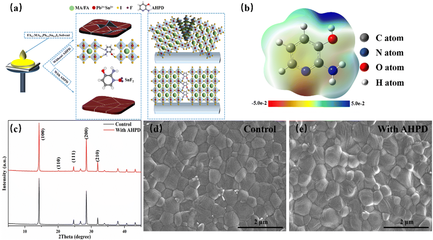 | ||
| Fig. 1 (a) Schematic illustration of the interaction between perovskites and AHPD, and the effect of AHPD on the microstructure evolution of the films. (b) Theoretically calculated ESP of AHPD. Electron-rich and -deficient regions are presented with red and blue colors in the ESP map, respectively. (c) XRD patterns of control films and the AHPD-incorporated films. Top-view SEM images of the films without (d) and with AHPD (e). | ||
As shown in Fig. 1a, the unshared electron lone pair on the pyridine nitrogen atom of AHPD could coordinate with the metal elements in the perovskite precursor solution (for example, PbI2, SnI2 and SnF2), playing a role in suppressing the oxidation process of Sn2+ to Sn4+. It is expected that the introduction of AHPD into the precursor solution could slow down the crystallization process and thus lead to more uniform films. Furthermore, the pyridine nitrogen, –OH and the enamine-like –NH2 of AHPD were expected to provide a means to passivate the electron-accepting (for example, halide vacancy, under-coordinated Pb2+/Sn2+) defects on the grain surfaces (Fig. 1a).
Fig. 1b illustrates the electrostatic potential maps used to identify the charge distributions of the AHPD molecule. By convention, red areas represent negative potential regions with high electron densities, which are relatively easy to donate electrons to a metal center. As can be observed, the pyridine nitrogen exhibits the largest negative potential (red), indicating that the pyridine nitrogen can be effectively used as a Lewis base to coordinate with Pb2+ or Sn2+, which is conducive to improving the crystallinity of perovskites.31–33 Furthermore, to verify the interaction between Pb2+/Sn2+ and AHPD, we obtained the 1H NMR spectra of AHPD dissolved in DMSO-d6 in the absence or presence of PbI2 (Fig. S1a, ESI†). Evident up-field shifts for aromatic proton signals in AHPD in the presence of PbI2 were observed, compared to those in the absence of PbI2. This was mainly ascribed to the strong coordinating interactions between the pyridine nitrogen and the Pb2+ ions, which led to the redistribution of the electron density along the molecular backbone. And the shifts for aromatic proton signals in AHPD in the presence of SnF2 (Fig. S1b, ESI†) revealed that the complex between AHPD and SnF2 was formed, which can effectively suppress the oxidation of Sn2+ similar to the results reported previously in the literature.34
The Fourier transform infrared spectroscopy (FTIR) was further performed on the perovskite powder without/with the AHPD additives introduced to investigate the interactions between AHPD and the perovskite materials (Fig. S2, ESI†). With the presence of AHPD in the Pb–Sn perovskite materials, it was shown that the characteristic C![[double bond, length as m-dash]](https://www.rsc.org/images/entities/char_e001.gif) N stretching vibration originally appeared at 1580 cm−1 blue-shifted to the lower wavenumber (1537 cm−1), indicating a strong interaction occurred between the pyridine nitrogen and the Pb2+/Sn2+ metal ion.35–37
N stretching vibration originally appeared at 1580 cm−1 blue-shifted to the lower wavenumber (1537 cm−1), indicating a strong interaction occurred between the pyridine nitrogen and the Pb2+/Sn2+ metal ion.35–37
Interestingly, it was found that the perovskite film without AHPD turned brown immediately after spin coating, which indicated the formation of perovskite nuclei (brown nuclei would gradually grow into complete perovskite grains). In contrast, the color change of the perovskite films obtained from the precursor solution with AHPD was much slower after spin coating (Fig. S3a, ESI†). Fig. S3b (ESI†) shows the photographs of FA0.7MA0.3Pb0.5Sn0.5I3 films with and without AHPD incorporated after annealing at 100 °C, which demonstrated the retarded crystallization of perovskites when AHPD was present. These results suggested that the addition of AHPD in the precursor solution could significantly retard the nucleation rate, which was slower than the crystal growth rate, facilitating the growth of large grains for the smooth and pinhole-free perovskite films.
In order to further explore how AHPD influenced the crystallization of the perovskite materials, XRD measurements were conducted on the perovskite films with and without AHPD (Fig. S4, ESI†). As shown in Fig. 1c, the XRD images of the films with and without AHPD showed two obvious peaks at 14.1° and 28.5° corresponding to the (100) and (200) planes in the tetragonal I4cm space group, which is in accord with results reported in the literature.18,38 It can be seen that the peak intensity of the films containing AHPD was obviously enhanced, indicating that the introduction of AHPD enhanced the crystallinity of the films. Besides, no characteristic diffraction peaks of 2D perovskite were observed for AHPD-incorporated films, which indicated that the AHPD molecules were located on the crystal surfaces instead of being inserted into the crystal lattice of the perovskites.39
We further investigated the effect of AHPD additives on the morphology of perovskite thin films using a field-emission scanning electron microscope (SEM). The surface morphology of the perovskite film (Fig. 1d and e) and the cross-sectional image of the device (Fig. S5a, ESI†) were obtained. It is clear that the surface of the control film showed a large number of fine grains without complete growth, where defects can be easily formed. With AHPD introduced, the grain size of the perovskite film was significantly enlarged (from 430 nm to 520 nm, Fig. S5b–d, ESI†), and the film became more compact. The increased grain size and the more compact perovskite films were expected to be able to reduce the recombination rate at the grain boundary and interface of the perovskite film and promote the device's performance.
Atomic force microscopy (AFM) and Kelvin probe force microscopy (KPFM) were used to detect the surface roughness and potential difference of perovskite films. Fig. 2a and b show that the root mean square (RMS) of roughness for the perovskite films without/with the AHPD additives changed from 16.5 nm to 9.89 nm, indicating that the surface became smoother due to the decreased crystal growth rate by the addition of AHPD. High-quality films could improve the interfacial contact between the perovskite materials and the PCBM electron-transporting layer (ETL), which would effectively reduce the density of defect states and be favorable for charge transfer. The mean contact potential difference (CPD) of the AHPD-incorporated film was found to be −139 mV, lower than that of the control film (−74 mV) (Fig. 2d and e), which indicated that the addition of AHPD effectively suppressed the formation of the unnecessary p-type doping.40–42 To better visualize this concept, the linear profile of the CPD value is shown in Fig. 2f. It was shown that compared with the control film in the whole region, the signal of the AHPD-incorporated film is more uniform. This result confirmed that the addition of AHPD lead to the passivation of defects on the top of the film surfaces and at grain boundaries, both of which would be favorable for the improvement of the device's performance.
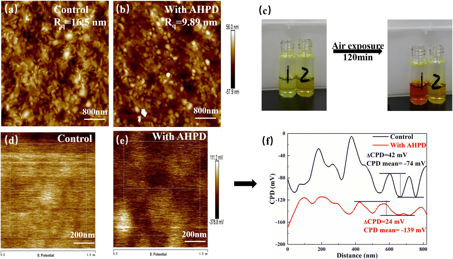 | ||
| Fig. 2 AFM images of control films (a) and films with AHPD (b). (c) Photographs of the perovskite precursor solutions without (marked as “1”) and with AHPD (marked as “2”) present in ambient air. KPFM images of control films (d) and AHPD films (e). (f) CPD linear spectra of control films and AHPD-involved films. | ||
We next examined the contact angle between the perovskite precursor solution and the substrate (Fig. S6, ESI†). We found that the contact angle θ increased from 14.08° to 17.80° after the incorporation of AHPD in the perovskite precursor solution. According to the classical free energy diagram of heterogeneous nucleation and the LaMer model,42–44 large θ resulted from the enhanced heterogeneous nucleation barrier, which slowed down the crystallization process and led to the increased grain size. These results could also further clarify the origin of the smoother perovskite film formed with the introduction of the AHPD additives.
3.2 The role of AHPD in suppressing Sn2+ oxidation
To evaluate the role played by AHPD in suppressing the oxidation of Sn2+ to Sn4+, we compared the color change of the perovskite precursor solutions in air with/without the presence of AHPD. Fig. 2c showed that both precursor solutions (both with SnF2 added) exhibited a light-yellow color initially. For the control (without AHPD), it can be observed that the solution turned dark red (the color of Sn4+ solution) after 120 min, whereas the solution with AHPD almost remained the initial yellow color. These results demonstrated the potential of using AHPD to retard the oxidation of Sn2+ in the precursor solution. We believed that the coordinating interaction between the basic nitrogen atom in the pyridine unit of AHPD and Sn2+ could play a role in stabilizing the Sn2+ ions and thus suppressing the oxidation of Sn2+ to Sn4+, thereby reducing p-type self-doping, which further validated the results obtained in the above-mentioned CPD.The chemical valence state of Sn elements and the interaction between Pb/Sn element and AHPD on the perovskite surface was further investigated by XPS measurements (Fig. 3a and b). For the pristine FA0.7MA0.3Pb0.5Sn0.5I3 film in the absence of AHPD, Sn 3d3/2 and Sn 3d5/2 peaks were located at 495.1 and 486.6 eV, respectively. The detailed deconvolution of these two peaks is associated with Sn4+ (487.3 and 495.7 eV) and Sn2+ (486.6 and 495.0 eV). It was calculated that Sn2+ and Sn4+ accounted for 55.48% and 44.52%, respectively, of the Sn element in the control film. After the introduction of AHPD, it was observed that the Sn4+ proportion decreased to 34.44%, while the Sn2+ increased to 65.56%, implying that the presence of AHPD significantly suppressed the oxidation of Sn2+ to Sn4+ during the film-forming process.
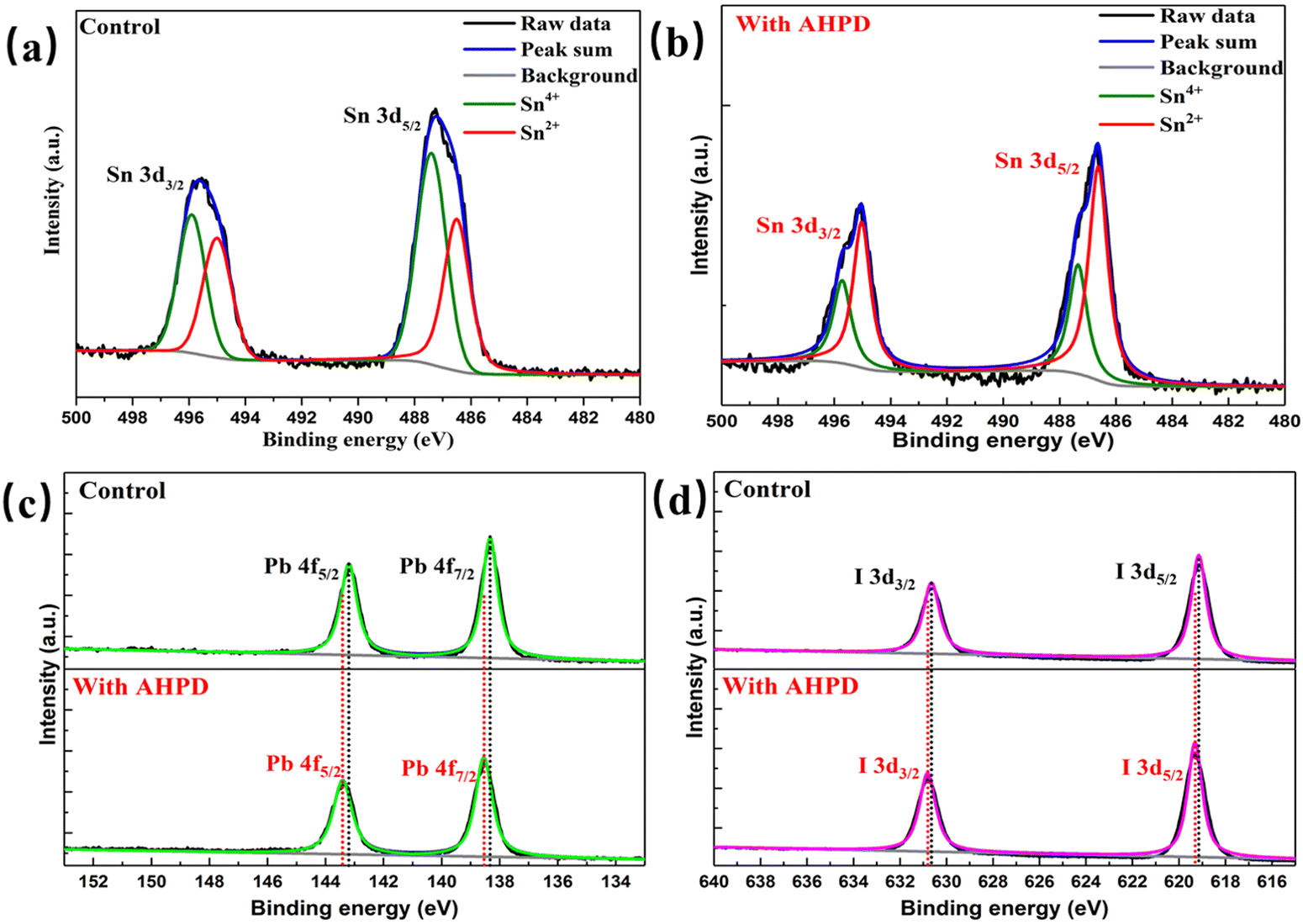 | ||
| Fig. 3 Sn 3d XPS spectra of control films (a) and films with AHPD (b). (c) Pb 4f XPS spectra of control films and films with AHPD. (d) I 3d XPS spectra of control films and films with AHPD. | ||
Interestingly, with the incorporation of AHPD, the Sn 3d signals shifted to higher BEs of 495.5 eV and 487.1 eV. Furthermore, Pb 4f signals for the AHPD-involved FA0.7MA0.3Pb0.5Sn0.5I3 also shifted to higher BEs (138.54 and 143.41 eV) compared to those for the Pb–Sn mixed perovskite with no AHPD added (138.33 and 143.20 eV), as shown in Fig. 3c. These results suggested that the passivating interaction occurred between AHPD and the undercoordinated Pb2+/Sn2+ ions on the perovskite surface. Furthermore, it was observed that the I 3d3/2 and I 3d5/2 (Fig. 3d) signals for the AHPD-incorporated perovskite films also moved to higher BEs. This transformation may be related to the disturbance of the static interaction between Pb2+/Sn2+ and I− at the interface caused by the coordination effect of AHPD on Pb2+/Sn2+. Overall, it is clearly shown that the coordinating interaction between AHPD and Pb2+/Sn2+ occurred, which could effectively passivate the defects present at the grain boundary and on the surface of the AHPD-incorporated FA0.7MA0.3Pb0.5Sn0.5I3 film. On the other hand, inhibition of the Sn4+ formation via the antioxidant role played by AHPD could also effectively reduce the trap density.
3.3 Photovoltaic performance and device stability
We then fabricated inverted p–i–n mixed Pb–Sn PSCs with an architecture of indium tin oxide (ITO)/poly(3,4-ethylenedioxythiophene)-poly(styrenesulfonate) (PEDOT:PSS)/perovskite/C60/bathocuproine (BCP)/Ag (Fig. S7, ESI†). We examined the influence of the AHPD additive at different concentrations from 1 to 3 mol% on the photovoltaic performance, as shown in Fig. S8 and Table S2 (ESI†). Notably, the device with 2 mol% AHPD achieved the highest PCE. As shown in Fig. 4a, the best (average) control device with an active area of 0.0625 cm2 showed a PCE of 15.72% (15.05%), an open-circuit voltage (VOC) of 0.6907 (0.6761) V, a short circuit current density (JSC) of 30.68 (30.08) mA cm−2 and a fill factor (FF) of 74.18% (74.16%). Encouragingly, it was shown that after the incorporation of 2 mol% AHPD as additives, the target device achieved a much higher PCE of 19.18% (18.78%), with a VOC of 0.8075 (0.7996) V, a JSC of 30.03 (30.06) mA cm−2, and a FF of 79.10% (78.16%). Moreover, to verify the universality of this additive, we added it into MAPb0.6Sn0.4I3 devices, which is another common tin-lead mixed perovskite structure, and attained one of the best PCE (14.62%) for MA-based narrow band gap perovskite solar cells, which is increased by nearly 34% compared to the control (10.92%). It can be observed from Fig. 4b, c and Fig. S9–S11 (ESI†) that compared with that of the control device, the improved PCE of the AHPD-incorporated devices could be attributed to the enhancement of all the photovoltaic parameters, especially VOC and FF values, which should be ascribed to the presence of the AHPD additives favoring the better interface contact, inhibition of the p-doping level defects and passivation of perovskite defects. The integrated JSC value of the control device was found to be 28.52 mA cm−2 and that of the device incorporated with 2 mol% AHPD was 28.68 mA cm−2 (Fig. 4d), which matched well with the values obtained from the J–V curves (<5% discrepancy).45,46 Both the control and AHPD-incorporated devices show a broad spectrum response from UV 300 nm to NIR 1100 nm, which was attributed to the narrow bandgap of FA0.7MA0.3Pb0.5Sn0.5I3. It was also shown that the JSC values obtained for the AHPD-incorporated device were greater over the spectral range of 800–900 nm compared to that for the control device, suggesting that the AHPD-incorporated devices exhibited improved charge collection and extraction capabilities. The stable output of photocurrent densities and the steady-state PCEs was measured at the maximum power point for the control and 2 mol% AHPD-incorporated devices, respectively. As displayed in Fig. S12 (ESI†), the AHPD-incorporated and control PSCs exhibited a stabilized PCE of 17.99% and 14.93%, respectively. To demonstrate the reproducibility of the devices, the statistical photovoltaic parameters for 15 devices are shown in Fig. S9 (ESI†). For the devices incorporated with AHPD at different concentrations, the PCE improved from 15.05 ± 0.62% to 18.78 ± 0.36%. In addition, we also test the long-term operational stability of the unencapsulated PSCs by exposing devices to ambient air at 20 ± 5 °C and 30 ± 5% RH for 350 h, shown in Fig. S14 (ESI†). Compared with the control device can only retain 22.5% of the initial PCE after 110 h. The PSC treated with AHPD can retain 47% of the initial PCE after 350 h.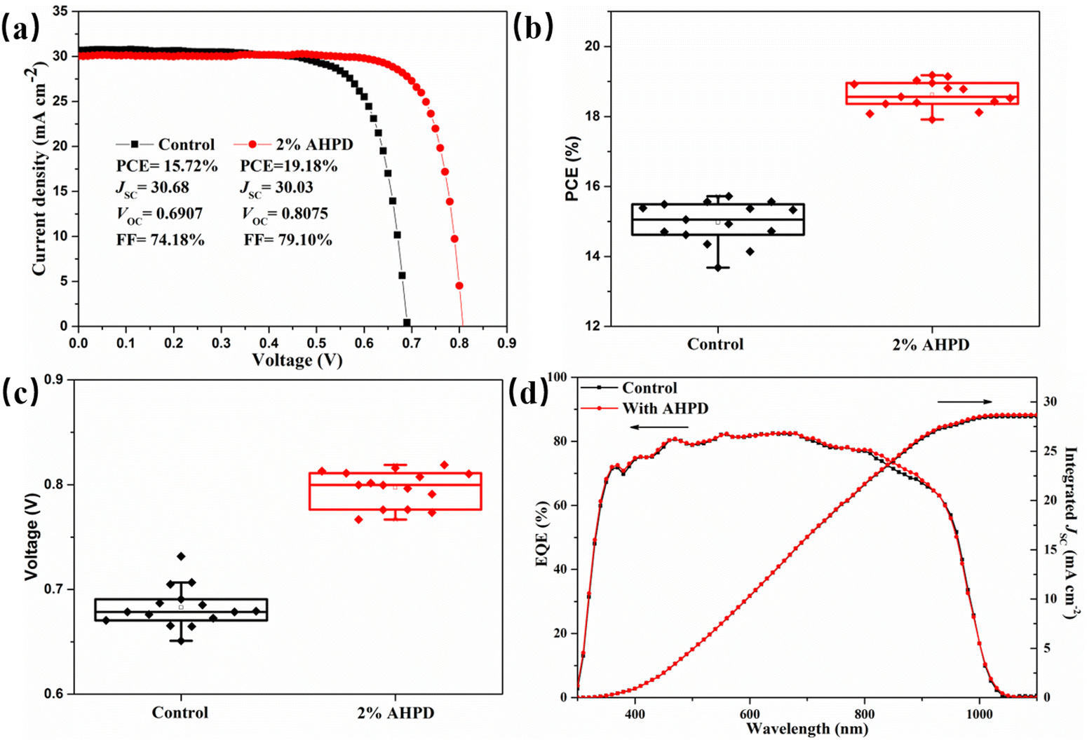 | ||
| Fig. 4 (a) J−V curves of the champion AHPD-treated and control devices with a reverse scan. (b) PCE distribution of the control and AHPD-treated devices. (c) VOC distribution of the control and AHPD-treated devices. (d) EQE spectra of the champion AHPD-treated and control devices, and the corresponding integrated JSC curves. | ||
3.4 Band structure of AHPD-incorporated perovskite films
Fig. 5a exhibits the light absorption spectra of the FA0.7MA0.3Pb0.5Sn0.5I3 perovskite films without any additives and with 2 mol% AHPD. According to the absorption edges, the incorporation of AHPD slightly increased the bandgap of FA0.7MA0.3Pb0.5Sn0.5I3 (without AHPD) from 1.260 eV to 1.262 eV. The absorption spectra of the FA0.7MA0.3Pb0.5Sn0.5I3 perovskite films incorporated with AHPD at different concentrations are shown in Fig. S15a (ESI†). There is no distinct difference among the control and the AHPD-incorporated perovskite films in absorption spectra, suggesting that the incorporation of AHPD does not influence the major crystal structure of perovskites. The perovskite films without AHPD (control film) and with 2% AHPD were then characterized by ultraviolet photoelectron spectroscopy (UPS) measurements (Fig. S15b, ESI†). In UPS analysis, the valence band position (EVB) of the film can be estimated by the equation EVB = WF + VBM, where WF and VBM represent the work function and valence band maximum of the perovskite film, respectively, and WF is derived from the cutoff energy (Ecutoff) by WF = 21.22 eV − Ecutoff.47 From the secondary electron cut-off of both films (Fig. 5c), the work function (WF) was derived to be 4.86 eV for the control film and 4.69 eV for the AHPD-incorporated film. This WF shift indicates that the AHPD-incorporated films exhibited more n-type characteristics, which was probably due to the reduction of Sn4+ to Sn2+. Also, fitting the valence band spectra of the control and AHPD-incorporated films in Fig. 5b, resulted in a VBM of 0.58 eV and 0.66 eV, respectively. By combining these band energy position results, we could calculate that EVB of the control and the AHPD-incorporated films are 5.44 eV and 5.35 eV, respectively. Then, we obtained the energy level alignment between the perovskite and other transport layers,47 as shown in Fig. S14c (ESI†). We can observe that EVB of AHPD-incorporated films was elevated, which was closer to the occupied molecular orbital (HOMO) of the PEDOT:PSS in our work. This band alignment can facilitate effective hole injection from the perovskite into the top electrode. Moreover, the AHPD-incorporated film with a much higher conduction band position could act as an efficient electron-blocking layer, a characteristic that could therefore suppress carrier recombination.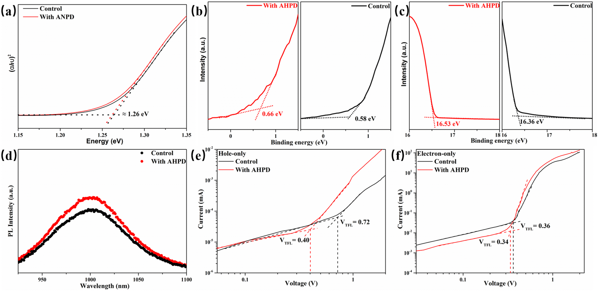 | ||
| Fig. 5 (a) Tauc plot of the control and AHPD incorporated perovskite. (b and c) Ultraviolet photoelectron spectra (UPS) of control films and AHPH films. (d) PL spectra of control films and AHPD films were deposited on bare glass substrates. SCLC characteristics of only hole devices (e) and only electron devices (f). | ||
3.5 Charge recombination and dynamics
Furthermore, the steady-state photoluminescence (PL) measurement was carried out for perovskite films without/with AHPD incorporated, which were deposited on the bare glass (Fig. 5d). The slight blue shift of the PL peak position (from 1003 without AHPD to 1015 nm with AHPD added) can be observed, indicating a slightly enlarged band gap, which was in accord with the results obtained from the absorption spectra. The enlarged band gap could be beneficial for the improvement of VOC. Compared to the control film, significant PL enhancement occurred for the AHPD-incorporated perovskite film, indicating that the nonradiative recombination defects on the surface of the film were suppressed due to the AHPD-induced improvement of perovskite crystallinity and optimization of film morphology.48–50To further evaluate the trap density (ntrap) across the perovskite films, we measured the space charge limited current (SCLC) on hole-only devices of FTO/PEDOT:PSS/FA0.7MA0.3Pb0.5Sn0.5I3 (with or without AHPD added)/spiro-OMeTAD/Ag under dark conditions (Fig. 5e and f). The dark I–V curves consist of three regions, including the ohmic region, the trap-filled limited (TFL) region and the trap-free SCLC region. In the ohmic region, the current shows linear relation to a bias voltage, and then it increases abruptly when the bias voltage exceeds the kink point, indicating the complete filling of trap states. The voltage at the kink point denotes the trap-filled limit voltage (VTFL), given by  , where ntrap is the trap density, e represents the electron charge, L is the thickness of the perovskite film, ε0 stands for the vacuum permittivity and ε is the relative dielectric constant of the perovskite. The VTFL value of the pristine FA0.7MA0.3Pb0.5Sn0.5I3 device was found to be 0.72 V, corresponding to a trap density of 1.4 × 1013 cm−3; whereas, the VTFL value was reduced to 0.40 V in the presence of the AHPD additive, leading to a lower trap density of 7.8 × 1012 cm−3. Similarly, the electron trap densities are measured to be 7.1 × 10¹² (VTFL = 0.36 V) and 6.6 × 10¹² (VTFL = 0.34 V) cm−3 (Fig. 5e and f) for devices with the structure FTO/SnO2/FA0.7MA0.3Pb0.5Sn0.5I3/PCBM/Ag. This result indicated that the incorporation of AHPD could significantly reduce the hole trap density caused by Sn2+ oxidation, reduce the nonradiative recombination loss and improve the device performance, which was consistent with the PL results.
Electrochemical impedance spectroscopy (EIS) measurements were carried out to further understand the mechanisms for the charge recombination and dynamics of the perovskite films and the corresponding devices. By fitting the EIS spectra at applied biases (0.45 V) under dark conditions, the evolution of resistance can be obtained (Fig. S16, ESI†). The corresponding equivalent circuit for fitting the curves is shown in the inset of Fig. S16 (ESI†), where Rs is the series resistance, R1 is the recombination resistance, and CPE1 is the chemical capacitance. All the PSCs exhibited the main semicircle at low frequency, which could be attributed to R1 and CPE1. The fitted R1 values for the AHPD-incorporated device were much lower than the control device. According to the previous literature,51,52 under low applied bias conditions, R1 was dominated by the charge transport of the perovskite film. We thus can conclude that the device with AHPD additives exhibited a better contact at the interface between the FA0.7MA0.3Pb0.5Sn0.5I3 layer and the C60 ETL, resulting in the improved JSC, VOC and FF for the AHPD-incorporated device as shown in Fig. 4a.
4. Conclusion
In summary, an effective additive AHPD was evaluated for the enhancement of Sn–Pb PSCs performance for the first time. It was shown that the incorporation of AHPD, which bears an effective pyridine in the molecule, in the FA0.7MA0.3Pb0.5Sn0.5I3 precursor solution could effectively suppress the Sn2+ oxidation and thus the p-doping level defects, resulting in the improved VOC. Furthermore, the pyridine nitrogen and the enamine-like –NH2 could retard the nucleation and crystallization rate by forming a coordinating interaction with PbI2/SnI2, resulting in forming large-grain film without pinholes. Moreover, the pyridine nitrogen, –OH and the enamine-like –NH2 also could passivate perovskite surface defects through the coordination with Pb2+/Sn2+ ions. We also noticed that the large band gap of AHPD-incorporated film facilitated effective hole injection from the perovskite into the PEDOT:PSS layer, while the higher conduction band position could prohibit the transfer of both electrons and holes from the FA0.7MA0.3Pb0.5Sn0.5I3 perovskite to the C60 layer. Moreover, the enhancement of hole mobility was noticed, which led to faster charge transfer at the perovskite and charge transport layer interfaces. As a result, the device with AHPD introduced exhibited a top PCE of 19.18% for narrow band gap perovskite solar cells, which is about 22% higher than that of the control device without the addition of AHPD (15.72% PCE). Moreover, the device with AHPD introduced exhibited a top PCE of 14.62% (Table S1, ESI†) for MA-based narrow band gap perovskite solar cells and with high reproducibility. Moreover, the device stability is also enhanced. This work provides a comprehensive understanding of the AHPD additive for use in the mixed Sn–Pb PSCs to modulate the process of crystallization and depress the Sn2+ oxidation and paves the way for realizing high performance narrow bandgap Sn–Pb PSCs in the future.Author contributions
W. C.: conceptualization, methodology, investigation, resources, data curation, and writing-original draft. K. S.: formal analysis and data curation. Y. H.: formal analysis and data curation. K. G. B.: writing-review and investigation. S. K.: writing-review and investigation. B. Z.: funding acquisition, supervision, and writing-review and editing. Y. F.: supervision, and writing-review and editing. M. K. N.: funding acquisition, supervision, and writing-review and editing. Y. Z.: conceptualization, methodology, data curation, writing-review and editing, and visualization.Conflicts of interest
The authors declare no competing financial interest.Acknowledgements
This work was financially supported by the Haihe Laboratory of Sustainable Chemical Transformations and the National Key Research and Development Program of China (2020YFB0408002).References
- A. Kojima, K. Teshima, Y. Shirai and T. Miyasaka, Organometal halide perovskites as visible-light sensitizers for photovoltaic cells, J. Am. Chem. Soc., 2009, 131(17), 6050–6051, DOI:10.1021/ja809598r.
- H. S. Kim, C. R. Lee and J. H. Im, et al., Lead Iodide Perovskite Sensitized All-Solid-State Submicron Thin Film Mesoscopic Solar Cell with Efficiency Exceeding 9%, Sci. Rep., 2012, 2, 591, DOI:10.1038/srep00591.
- R. Fickler, R. Lapkiewicz, W. N. Plick, M. Krenn, C. Schaeff, S. Ramelow and A. Zeilinger, Quantum entanglement of high angular momenta, Science, 2012, 338(6107), 640–643, DOI:10.1126/science.1227193.
- K. Su, P. Zhao, Y. Ren, Y. Zhang, G. Yang, Y. Huang, Y. Feng and B. Zhang, A Porphyrin-Involved Benzene-1,3,5-Tricarboxamide Dendrimer (Por-BTA) as a Multifunctional Interface Material for Efficient and Stable Perovskite Solar Cells, ACS Appl. Mater. Interfaces, 2021, 13(12), 14248–14257, DOI:10.1021/acsami.1c00146.
- M. Jeong, I. Woo Choi, E. Min Go, Y. Cho, M. Kim, B. Lee, S. Jeong, Y. Jo, H. Won Choi, J. Lee, J.-H. Bae, S. Kyu Kwak, D. Suk Kim and C. Yang, Stable perovskite solar cells with efficiency exceeding 24.8% and 0.3 V voltage loss, Science, 2020, 369, 1615–1620 CrossRef CAS PubMed.
- NREL (National Renewable Energy Lab), Best Research-Cell Efficiencies, July 5, 2022. https://www.nrel.gov/pv/assets/pdfs/cell-pv-eff-emergingpv-rev220630.pdf.
- J. Jeong, M. Kim, J. Seo, H. Lu, P. Ahlawat, A. Mishra, Y. Yang, M. A. Hope, F. T. Eickemeyer, M. Kim, Y. J. Yoon, I. W. Choi, B. P. Darwich, S. J. Choi, Y. Jo, J. H. Lee, B. Walker, S. M. Zakeeruddin, L. Emsley and J. Y. Kim, Pseudo-halide anion engineering for α-FAPbI3 perovskite solar cells, Nature, 2021, 592(7854), 381–385, DOI:10.1038/s41586-021-03406-5.
- Q. Chen, J. Luo, R. He, H. Lai, S. Ren, Y. Jiang, Z. Wan, W. Wang, X. Hao, Y. Wang, J. Zhang, I. Constantinou, C. Wang, L. Wu, F. Fu and D. Zhao, Unveiling Roles of Tin Fluoride Additives in High-Efficiency Low-Bandgap Mixed Tin-Lead Perovskite Solar Cells, Adv. Energy Mater., 2021, 11, 2101045, DOI:10.1002/aenm.202101045.
- S. Hu, K. Otsuka, R. Murdey, T. Nakamura and M. A. Truong, et al., Optimized carrier extraction at interfaces for 23.6% efficient tin–lead perovskite solar cells, Energy Environ. Sci., 2022, 15, 2096–2107, 10.1039/D2EE00288D.
- R. Lin, J. Xu and M. Wei, et al., All-perovskite tandem solar cells with improved grain surface passivation, Nature, 2022, 603, 73–78, DOI:10.1038/s41586-021-04372-8.
- C. Wang, Y. Zhao and T. Ma, et al., A universal close-space annealing strategy towards high-quality perovskite absorbers enabling efficient all-perovskite tandem solar cells, Nat. Energy, 2022, 7, 744–753, DOI:10.1038/s41560-022-01076-9.
- G. Kapil, T. Bessho, T. Maekawa, A. K. Baranwal, Y. Zhang, M. A. Kamarudin, D. Hirotani, Q. Shen, H. Segawa and S. Hayase, Tin-Lead Perovskite Fabricated via Ethylenediamine Interlayer Guides to the Solar Cell Efficiency of 21.74%, Adv. Energy Mater., 2021, 11, 2101069, DOI:10.1002/aenm.202101069.
- K. Zhang, K. Forberich, L. Lüer, J. G. Cerrillo, W. Meng, X. Du, V. M. Le Corre, Y. Zhao, T. Niu and Q. Xue, Understanding the Limitations of Charge Transporting Layers in Mixed Lead–Tin Halide Perovskite Solar Cells, Advanced Energy and Sustainability Research, 2021, 3, 2100156, DOI:10.1002/aesr.202100156.
- J. Cao, H. Loi, Y. Xu, X. Guo, N. Wang, C. Liu, T. Wang, H. Cheng, Y. Zhu and M. G. Li, High-Performance Tin–Lead Mixed-Perovskite Solar Cells with Vertical Compositional Gradient, Adv. Mater., 2022, 34, 2107729, DOI:10.1002/adma.202107729.
- C. C. Stoumpos, C. D. Malliakas and M. G. Kanatzidis, Semiconducting tin and lead iodide perovskites with organic cations: Phase transitions, high mobilities, and near-infrared photoluminescent properties, Inorg. Chem., 2013, 52(15), 9019–9038, DOI:10.1021/ic401215x.
- J. Xi, H. Duim, M. Pitaro, K. Gahlot, J. Dong, G. Portale and M. A. Loi, Scalable, Template Driven Formation of Highly Crystalline Lead-Tin Halide Perovskite Films, Adv. Funct. Mater., 2021, 31, 2105734, DOI:10.1002/adfm.202105734.
- J. Xi and M. A. Loi, The Fascinating Properties of Tin-Alloyed Halide Perovskites, ACS Energy Lett., 2021, 6(5), 1803–1810, DOI:10.1021/acsenergylett.1c00289.
- Z. Zhu, N. Li, D. Zhao, L. Wang and A. K. Y. Jen, Improved Efficiency and Stability of Pb/Sn Binary Perovskite Solar Cells Fabricated by Galvanic Displacement Reaction, Adv. Energy Mater., 2019, 9, 1802774, DOI:10.1002/aenm.201802774.
- K. Hamada, R. Tanaka, M. A. Kamarudin, Q. Shen, S. Iikubo, T. Minemoto, K. Yoshino, T. Toyoda, T. Ma, D. W. Kang and S. Hayase, Enhanced Device Performance with Passivation of the TiO2 Surface Using a Carboxylic Acid Fullerene Monolayer for a Sn–Pb Perovskite Solar Cell with a Normal Planar Structure, ACS Appl. Mater. Interfaces, 2020, 12(15), 17776–17782, DOI:10.1021/acsami.0c01411.
- Y. Zong, Z. Zhou, M. Chen, N. P. Padture and Y. Zhou, Lewis-Adduct Mediated Grain-Boundary Functionalization for Efficient Ideal-Bandgap Perovskite Solar Cells with Superior Stability, Adv. Energy Mater., 2018, 8, 1800997, DOI:10.1002/aenm.201800997.
- X. Xu, C. C. Chueh, Z. Yang, A. Rajagopal and A. K. Y. Jen, Ascorbic acid as an effective antioxidant additive to enhance the efficiency and stability of Pb/Sn-based binary perovskite solar cells, Nano Energy, 2017, 34, 392–398, DOI:10.1016/j.nanoen.2017.02.040.
- S. J. Lee, S. S. Shin, Y. C. Kim, D. Kim, T. K. Ahn, J. H. Noh, J. Seo and S. il Seok, Fabrication of Efficient Formamidinium Tin Iodide Perovskite Solar Cells through SnF2-Pyrazine Complex, J. Am. Chem. Soc., 2016, 138(12), 3974–3977, DOI:10.1021/jacs.6b00142.
- R. Lin, K. Xiao, Z. Qin, Q. Han, C. Zhang, M. Wei, M. I. Saidaminov, Y. Gao, J. Xu, M. Xiao, A. Li, J. Zhu, E. H. Sargent and H. Tan, Monolithic all-perovskite tandem solar cells with 24.8% efficiency exploiting comproportionation to suppress Sn(II) oxidation in precursor ink, Nat. Energy, 2019, 4(10), 864–873, DOI:10.1038/s41560-019-0466-3.
- H. Ban, Q. Sun, T. Zhang, H. Li, Y. Shen and M. Wang, Stabilization of Inorganic CsPb0.5Sn0.5I2Br Perovskite Compounds by Antioxidant Tea Polyphenol, Sol. RRL, 2020, 4, 1900457, DOI:10.1002/solr.201900457.
- H. Liu, L. Wang, R. Li, B. Shi, P. Wang, Y. Zhao and X. Zhang, Modulated Crystallization and Reduced VOC Deficit of Mixed Lead-Tin Perovskite Solar Cells with Antioxidant Caffeic Acid, ACS Energy Lett., 2021, 6(8), 2907–2916, DOI:10.1021/acsenergylett.1c01217.
- G. Cavallo, P. Metrangolo, R. Milani, T. Pilati, A. Priimagi, G. Resnati and G. Terraneo, The halogen bond, Chem. Rev., 2016, 116(4), 2478–2601, DOI:10.1021/acs.chemrev.5b00484.
- Y. Chen, H. Yu, L. Zhang, H. Yang and Y. Lu, Photoresponsive liquid crystals based on halogen bonding of azopyridines, Chem. Commun., 2014, 50(68), 9647–9649, 10.1039/c4cc02344g.
- K. Zhu, S. Cong and Z. Lu, et al., Enhanced perovskite solar cell performance via defect passivation with ethylamine alcohol chlorides additive, J. Power Sources, 2019, 428(15), 82–87, DOI:10.1016/j.jpowsour.2019.04.056.
- M. J. Choi, Y. S. Lee and I. H. Cho, et al., Functional additives for high-performance inverted planar perovskite solar cells with exceeding 20% efficiency: selective complexation of organic cations in precursors, Nano Energy, 2020, 71, 104639, DOI:10.1016/j.nanoen.2020.104639.
- R. Wang, J. Xue and K. L. Wang, et al., Constructive molecular configurations for surface-defect passivation of perovskite photovoltaics, Science, 2019, 366(6472), 1509–1513, DOI:10.1126/science.aay9698.
- W. Ke and M. G. Kanatzidis, Prospects for low-toxicity lead-free perovskite solar cells, Nat. Commun., 2019, 10, 965, DOI:10.1038/s41467-019-08918-3.
- I. Chung, J. H. Song, J. Im, J. Androulakis, C. D. Malliakas, H. Li, A. J. Freeman, J. T. Kenney and M. G. Kanatzidis, CsSnI 3: Semiconductor or metal? High electrical conductivity and strong near-infrared photoluminescence from a single material. High hole mobility and phase-transitions, J. Am. Chem. Soc., 2012, 134(20), 8579–8587, DOI:10.1021/ja301539s.
- M. Kunitski, N. Eicke, P. Huber, J. Köhler, S. Zeller, J. Voigtsberger, N. Schlott, K. Henrichs, H. Sann, F. Trinter, L. P. H. Schmidt, A. Kalinin, M. S. Schöffler, T. Jahnke, M. Lein and R. Dörner, Double-slit photoelectron interference in strong-field ionization of the neon dimer, Nat. Commun., 2019, 10, 1, DOI:10.1038/s41467-018-07882-8.
- J. Cao, H. L. Loi, Y. Xu, X. Guo, N. Wang and C. K. Liu, et al., High-Performance Tin–Lead Mixed-Perovskite Solar Cells with Vertical Compositional Gradient, Adv. Mater., 2020, 34, 2107729, DOI:10.1002/adma.202107729.
- S. Shao, J. Dong, H. Duim, G. H. ten Brink, G. R. Blake, G. Portale and M. A. Loi, Enhancing the crystallinity and perfecting the orientation of formamidinium tin iodide for highly efficient Sn-based perovskite solar cells, Nano Energy, 2019, 60, 810–816, DOI:10.1016/j.nanoen.2019.04.040.
- D. H. Cao, C. C. Stoumpos, T. Yokoyama, J. L. Logsdon, T. Song, O. K. bin, Farha, M. R. Wasielewski, J. T. Hupp and M. G. Kanatzidis, Thin Films and Solar Cells Based on Semiconducting Two-Dimensional Ruddlesden-Popper (CH3(CH2)3NH3)2(CH3NH3)n-1SnnI3n+1 Perovskites, ACS Energy Lett., 2017, 2(5), 982–990, DOI:10.1021/acsenergylett.7b00202.
- Y. Liao, H. Liu, W. Zhou, D. Yang, Y. Shang, Z. Shi, B. Li, X. Jiang, L. Zhang, L. N. Quan, R. Quintero-Bermudez, B. R. Sutherland, Q. Mi, E. H. Sargent and Z. Ning, Highly Oriented Low-Dimensional Tin Halide Perovskites with Enhanced Stability and Photovoltaic Performance, J. Am. Chem. Soc., 2017, 139(19), 6693–6699, DOI:10.1021/jacs.7b01815.
- W. Liao, D. Zhao, Y. Yu, N. Shrestha, K. Ghimire, C. R. Grice, C. Wang, Y. Xiao, A. J. Cimaroli, R. J. Ellingson, N. J. Podraza, K. Zhu, R. G. Xiong and Y. Yan, Fabrication of Efficient Low-Bandgap Perovskite Solar Cells by Combining Formamidinium Tin Iodide with Methylammonium Lead Iodide, J. Am. Chem. Soc., 2016, 138(38), 12360–12363, DOI:10.1021/jacs.6b08337.
- R. Wang, J. Xue, K.-L. Wang, Z.-K. Wang, Y. Luo, D. Fenning, G. Xu, S. Nuryyeva, T. Huang, Y. Zhao, J. Lee Yang, J. Zhu, M. Wang, S. Tan, I. Yavuz, K. N. Houk and Y. Yang, Constructive molecular configurations for surface-defect passivation of perovskite photovoltaics, Science, 2019, 366, 1509–1513, DOI:10.1126/science.aay9698.
- S. Xiong, Z. Hou, S. Zou, X. Lu, J. Yang, T. Hao, Z. Zhou, J. Xu, Y. Zeng, W. Xiao, W. Dong, D. Li, X. Wang, Z. Hu, L. Sun, Y. Wu, X. Liu, L. Ding, Z. Sun, M. Fahlman and Q. Bao, Direct Observation on p- to n-Type Transformation of Perovskite Surface Region during Defect Passivation Driving High Photovoltaic Efficiency, Joule, 2021, 5(2), 467–480, DOI:10.1016/j.joule.2020.12.009.
- J. Tan, W. Yang, H. Lee, J. Park, K. Kim, O. S. Hutter, L. J. Phillips, S. Shim, J. Yun, Y. Park, J. Lee, J. D. Major and J. Moon, Surface restoration of polycrystalline Sb2Se3 thin films by conjugated molecules enabling high-performance photocathodes for photoelectrochemical water splitting, Appl. Catal., B, 2021, 286, 119890, DOI:10.1016/j.apcatb.2021.119890.
- X. Meng, Y. Li, Y. Qu, H. Chen, N. Jiang, M. Li, D. J. Xue, J. S. Hu, H. Huang and S. Yang, Crystallization Kinetics Modulation of FASnI3 Films with Pre-nucleation Clusters for Efficient Lead-Free Perovskite Solar Cells, Angew. Chem., Int. Ed., 2021, 60(7), 3693–3698, DOI:10.1002/anie.202012280.
- A. R. Pascoe, Q. Gu, M. U. Rothmann, W. Li, Y. Zhang, A. D. Scully, X. Lin, L. Spiccia, U. Bach and Y. B. Cheng, Directing nucleation and growth kinetics in solution-processed hybrid perovskite thin-films, Sci. China Mater., 2017, 60(7), 617–628, DOI:10.1007/s40843-017-9043-y.
- J. H. Heo, D. H. Song and S. H. Im, Planar CH3NH3PbBr3 hybrid solar cells with 10.4% power conversion efficiency, fabricated by controlled crystallization in the spin-coating process, Adv. Mater., 2014, 26(48), 8179–8183, DOI:10.1002/adma.201403140.
- A. K. Dhara, S. Maity and B. B. Dhar, Visible-light-mediated synthesis of substituted phenazine and phenoxazinone using eosin y as a photoredox catalyst, Org. Lett., 2021, 23(9), 3269–3273, DOI:10.1021/acs.orglett.1c00725.
- B.-B. Yu, L. Xu, M. Liao, Y. Wu, F. Liu, Z. He, J. Ding,W. Chen, B. Tu, Y. Lin, Y. Zhu, X. Zhang, W. Yao, A. B. Djurisic, J.-S. Hu and Z. He, Synergy Effect of Both 2,2,2-TrifluoroethylamineHydrochloride and SnF2 for Highly Stable FASnI3-xClx Perovskite Solar Cells, Solar RRL, 2019, 3, 1800290, DOI:10.1002/solr.201800290.
- Q. Jiang, Z. Chu, P. Wang, X. Yang, H. Liu, Y. Wang, Z. Yin, J. Wu, X. Zhang and J. You, Planar-Structure Perovskite Solar Cells with Efficiency beyond 21%, Adv. Mater., 2017, 29, 1703852, DOI:10.1002/adma.201703852.
- G. Kapil, T. Bessho, C. H. Ng, K. Hamada, M. Pandey, M. A. Kamarudin, D. Hirotani, T. Kinoshita, T. Minemoto, Q. Shen, T. Toyoda, T. N. Murakami, H. Segawa and S. Hayase, Strain Relaxation and Light Management in Tin-Lead Perovskite Solar Cells to Achieve High Efficiencies, ACS Energy Lett., 2019, 4(8), 1991–1998, DOI:10.1021/acsenergylett.9b01237.
- C. Xu, Y. Yao, G. Wang, J. Dong, G. Xu, Y. Zhong, D. Lu, X. Zhao, D. Liu, G. Zhou, X. Yang, P. Li, L. Chen and Q. Song, Self-woven monolayer polyionic mesh to achieve highly efficient and stable inverted perovskite solar cells, Chem. Eng. J., 2022, 428, 132074, DOI:10.1016/j.cej.2021.132074.
- Q. Jiang, Y. Zhao, X. Zhang, X. Yang, Y. Chen, Z. Chu, Q. Ye, X. Li, Z. Yin and J. You, Surface passivation of perovskite film for efficient solar cells, Nat. Photonics, 2019, 13(7), 460–466, DOI:10.1038/s41566-019-0398-2.
- D. Pitarch-Tena, T. T. Ngo, M. Vallés-Pelarda, T. Pauporté and I. Mora-Seró, Impedance Spectroscopy Measurements in Perovskite Solar Cells: Device Stability and Noise Reduction, ACS Energy Lett., 2018, 3, 1044–1048, DOI:10.1021/acsenergylett.8b00465.
- I. Zarazua, G. Han, P. P. Boix, S. Mhaisalkar, F. Fabregat-Santiago, I. Mora-Seró, J. Bisquert and G. Garcia-Belmonte, Surface Recombination and Collection Efficiency in Perovskite Solar Cells from Impedance Analysis, J. Phys. Chem. Lett., 2016, 7(24), 5105–5113, DOI:10.1021/acs.jpclett.6b02193.
Footnote |
| † Electronic supplementary information (ESI) available: Methods and additional figures and tables. See DOI: https://doi.org/10.1039/d2tc04000j |
| This journal is © The Royal Society of Chemistry 2023 |